
D7.16 - Progress Activity Report #2 · Progress Activity Report #2 Covered period ... Substrate...
38
CARBON BASED SMART SYSTEM FOR WIRELESS APPLICATION Start Date : 01/09/12 Project n° 318352 Duration : 36 months Topic addressed : Very advanced nanoelectronic components: design, engineering, technology and manufacturability WORK PACKAGE 7 : Project management DELIVERABLE D7.16 Progress Activity Report #2 Covered period: T0+6 – T0+12 Due date : T0+12 Submission date : T0+13 Lead contractor for this deliverable: TRT Dissemination level : PU – Public
Transcript of D7.16 - Progress Activity Report #2 · Progress Activity Report #2 Covered period ... Substrate...
CARBON BASED SMART SYSTEM FOR WIRELESS APPLICATION
Start Date : 01/09/12 Project n° 318352 Duration : 36 months Topic addressed : Very advanced nanoelectronic comp onents: design, engineering, technology and manufacturability
WORK PACKAGE 7 : Project management
DELIVERABLE D7.16
Progress Activity Report #2 Covered period: T0+6 – T0+12
Due date : T0+12 Submission date : T0+13
Lead contractor for this deliverable: TRT
Dissemination level : PU – Public
D7.16 - Progress Activity Report #2 (T0+6 – T0+12)
2/38
2
WORK PACKAGE 7: Project management
PARTNERS ORGANISATION APPROVAL
Name Function Date Signature
Prepared by: S.Xavier R&D Engineer 01/10/13
Approved by: Afshin Ziaei Research Program Manager
01/10/13
DISTRIBUTION LIST
QUANTITY ORGANIZATION NAMES
1 ex Thales Research and Technology TRT Afshin ZIAEI
1 ex Chalmers University of Technology CHALMERS Johan LIU
1 ex Foundation for Research & Technology - Hellas FORTH George KONSTANDINIS
1 ex Laboratoire d’Architecture et d’Analyse des Systèmes
CNRS-LAAS George DELIGEORGIS
1 ex Université Pierre et Marie Curie UPMC Charlotte TRIPON-CANSELIET
1 ex National Research and Development Institute for Microtechnologies
IMT Mircea DRAGOMAN
1 ex Graphene Industries GI Peter BLAKE
1 ex Thales Systèmes Aéroportés TSA Yves MANCUSO
1 ex SHT Smart High-Tech AB SHT Yifeng FU
1 ex Universita politecnica delle Marche UNIVPM Luca PIERANTONI
1 ex Linköping University LiU Rositsa YAKIMOVA
1 ex Fundacio Privada Institute Catala de Nanotecnologia
ICN Clivia SOTOMAYOR
1 ex Tyndall-UCC Tyndall Mircea MODREANU

D7.16 - Progress Activity Report #2 (T0+6 – T0+12)
3/38
3
CHANGE RECORD SHEET
REVISION LETTER DATE PAGE NUMBER DESCRIPTION
v0 07/2013 10 Initial version
v1 30/09/2013 30 All partners contributions
v2 01//10/2013 38 Final version

D7.16 - Progress Activity Report #2 (T0+6 – T0+12)
4/38
4
CONTENTS
1 PROJECT OBJECTIVES AND MAJOR ACHIEVEMENTS DURING RE PORTING PERIOD (T0+6 – T0+12) 7
2 MANAGEMENT ACTIVITIES (WP7) 8
2.1 MEETING 8
3 PROGRESS IN THE ACTIVE THECNICAL WORKPACKAGE 2 9
3.1 WP2 : DESIGN AND SIMULATION ACTIVITIES 9
3.1.1 WP OBJECTIVES 9
3.1.2 PROGRESS TOWARD OBJECTIVES : STATUS OF ACTIVES TASKS 9 3.1.2.1 Task 2.2: Design of the CNT based RF switch (TRT/IMT) 9 3.1.2.2 Task 2.3 : Design of the CNT filter/oscillator (LAAS/IMT) 10 3.1.2.3 Task.2.5 Design and simulation of RF graphene devices(IMT) 11
4 PROGRESS IN THE ACTIVE THECNICAL WORKPACKAGE 3 12
4.1 WP3 : FABRICATION ACTIVITIES 12
4.2 WP OBJECTIVES 12
4.2.1 PROGRESS TOWARD OBJECTIVES : STATUS OF ACTIVES TASKS 13 4.2.1.1 Task.3.1 CNT and graphene growth technology 13 4.2.1.2 Task.3.2 CNT and graphene material characterization 17 4.2.1.3 Task.3.3 Fabrication of CNT FET 20 4.2.1.4 Task.3.4 CNT RF switch fabrication (TRT) 21 4.2.1.5 Task.3.6 CNT based antenna fabrication (TRT/SHT/UPMC) 23 4.2.1.6 Task.3.7 Development of carbon nanotube interconnects (SHT/CHALMERS) 25 4.2.1.7 Task.3.8 Development of RF graphene devices 26
Substrate optimization 32
5 DISSEMINATION AND EXPLOITATION ACTIVITIES (WP6) 38
5.1 PUBLICATIONS & CONFERENCE 38
D7.16 - Progress Activity Report #2 (T0+6 – T0+12)
5/38
5
FIGURES Figure 1 : NANO-RF Timetable ................................................................................................................... 8
Figure 2 : RF NEMS design.......................................................................................................................10
Figure 3: Displacement and Capacitance change of a CNT which flexes under an applied bias .........10
Figure 4 : The graphene antenna in CST..................................................................................................11
Figure 5 : S11 as a function of frequency.................................................................................................11
Figure 6 : Radiation patter for the graphene antenna at 9.5GHz............................................................12
Figure 7 : (a) Process flow for the TiN/Ni catalyst dots fabrication; (b) SEM picture of the 1µm bilayer resist before TiN/Ni deposition...........................................................................................................14
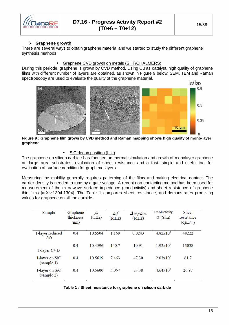
Figure 8 : 1µm and 250nm TiN/Ni catalyst dots and CNT growth performed by SHT on this sample...14
Figure 9 : Graphene film grown by CVD method and Raman mapping shows high quality of mono-layer graphene ..............................................................................................................................................15
Figure 10 : Test sample of large area (15 x 15 mm, right image) to previous generation graphene on SiC (7 x 7 mm, left image)...................................................................................................................16
Figure 11 : Image with monolayer graphene on SiC, darker steps are due to bilayer areas.................16
Figure 12 : Multi Walls CNT bundle growth process description.............................................................18
Figure 13: Narrow bandpass filters available for optical contrast measurements. The range covers the visible spectrum. The 560 nm filter is used for this project because it maximises contrast for flakes
on 300 nm SiO₂. ..................................................................................................................................20
Figure 14: Left: colour micrograph of flake 4 on sample S8111. Right: monochrome image of the same flake with λ=560nm illumination. The white numbers on various regions of the flake display the number of graphene layers – determined using optical contrast measurements............................20
Figure 15 : Horizontally aligned CNTs grown on quartz substrate ..........................................................21
Figure 16 : AFM scanning of SWCNTs grown on quartz substrate ........................................................21
Figure 17 : Process flow for the RF NEMS switch...................................................................................22
Figure 18 : RF NEMS fabrication at different step...................................................................................23
Figure 19 : Input impedance in frequency of a 750um-length CNT-based monopole antenna integrated on quartz substrate with different MW CNT bundle surface reactance from 0.001 to 1 Ω.m2 - Taper length: 200 um – MW CNT bundle diameter: 6 um – MW CNT resistance: 0.01 Ω.m2 .................24
Figure 20 : First experimental microwave test structure configuration (c) of MW CNT bundle monopole on doped Si wafer (a) after wafer dicing/etching (TRT/MC2) and report on quartz substrate (b) implemented inside a protected microwave mounting with a 2,4 mm/50Ω coaxial access (with technical support of sub-contractor IEMN/MC2)...............................................................................25
Figure 21 : CNT bundles directly grown from TSVs .................................................................................25
Figure 22 : Transferring densified CNT bundles into TSVs.....................................................................25
Figure 23 : Transferring densified CNT bundles into TSV structure .......................................................26
Figure 24: TLM on GS material .................................................................................................................26
Figure 25: TLM on FORTH transfer..........................................................................................................26
Figure 26: Comparison of contacts...........................................................................................................26
Figure 27: Raman spectra of various FORTH transferred layers compared to GS..............................27
Figure 28: Ramp for resist bake “friendly” to graphene ...........................................................................27
Figure 29: SEM image before bake ..........................................................................................................27
Figure 30: SEM image after bake..............................................................................................................27
Figure 31: Graphene before ramped curing .............................................................................................28
Figure 32: Graphene after ramped curing ................................................................................................28
Figure 33: I-V characteristics of the various metallization.......................................................................28
Figure 34 : TLM results comparison .........................................................................................................29
D7.16 - Progress Activity Report #2 (T0+6 – T0+12)
6/38
6
Figure 35 : The optical constant dispersion for 90nm-thick Parylene N thin film....................................30
Figure 36 : The Raman spectrum of 90nm-thick Parylene N thin film.....................................................30
Figure 37: Raman analysis of SiN encapsulated graphene .................................................................... 31 Figure 38: EDX spectrum from naturally oxidized thin e-beam deposited aluminum layers.................. 31 Figure 40: AFM analysis of Pt bottom electrode of the test capacitors .................................................. 32 Figure 41: Fabricated capacitor ................................................................................................................ 32 Figure 42: conventional (left) and inverted (right) processing concepts. The latter provides a low loss
polymeric substrate and at the same time does not expose the sensitive graphene layer to any processing steps which reduces its contamination level................................................................... 32
Figure 43: Circuits shown fabricated using the “inverted process”......................................................... 33 Figure 44: SEM photo of a test T-gate...................................................................................................... 33 Figure 45: T-gate with S-D metal............................................................................................................... 33 Figure 46: X-section of T-Gate, the self-align effect is evident............................................................... 33 Figure 47: GS piece with GFETS .............................................................................................................. 34 Figure 48: I-V characteristics ....................................................................................................................34
Figure 49: 2nd GFET device, cracks in pyralene evident .........................................................................34
Figure 50: Snapshot of the GDS for the 3rd “generation” FORTH all e-beam GFET.............................35
Figure 51: Graphene Hall device on SiO2 ................................................................................................ 35 Figure 52: Fabrication of Hall new design for dielectric effect study....................................................... 36 Figure 53 : The graphene rectifier on wafer (arbitrary colors –graphene is blue).................................. 36 Figure 54 : The graphene rectifier.............................................................................................................37
Figure 55 : The graphene rectifier under measurement (Keithley 4200 SCS).......................................37
Figure 56 : I-V dependence .......................................................................................................................38
TABLES Table 1 : Sheet resistance for graphene on silicon carbide ....................................................................15
Table 2 : Information about the graphene flakes produced during the last 6 month...............................17
Table 3: TLM results (as deposited) .........................................................................................................28
Table 4 : TLM results of contact X-Y on GS graphene with binary..........................................................29

D7.16 - Progress Activity Report #2 (T0+6 – T0+12)
7/38
7
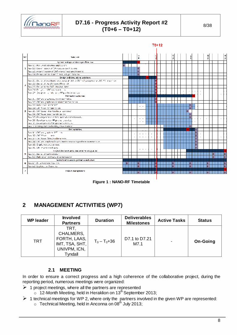
1 PROJECT OBJECTIVES AND MAJOR ACHIEVEMENTS DURING REPORTING PERIOD (T0+6 – T0+12) According to the timetable (see Figure 1), the project objectives over the reporting period are:
• Within the framework of WP 2 ‘Design and simulation activities’ : design and simulate all the
CNTs and graphene based sub-components forming the nano T/R module to be demonstrated in WP5 comprising filters/oscillators, switches, mixers, LNAs and PAs and finally an antenna. The main technical objectives are:
Design and modelling of CNT and graphene based FET and then design and modeling of LNA,PA and mixer based on either CNT or graphene
Design and modelling of CNT switch; Design and modelling of CNT filter/oscillator and graphene mixer Design and modelling of CNT antenna. Design and modelling of LNA based graphene Design and modelling of a graphene loaded antenna.
• Within the framework of WP 3 ‘Fabrication activities’ to: all the CNT and graphene based sub-
modules that have been designed in the work package 2. The principal objective of this work package is to fabricate the test structures and also final components based on the results of WP2
• Within the framework of WP 7 ‘Project Management’ : to establish durable basis for the project management and monitoring all along the project duration, through the following actions:
Regular project and technical meetings;
As described in the following sections, all these objectives have progressed between T0+6 and T0+12.
D7.16 - Progress Activity Report #2 (T0+6 – T0+12)
8/38
8
Figure 1 : NANO-RF Timetable
2 MANAGEMENT ACTIVITIES (WP7)
WP leader Involved Partners
Duration Deliverables Milestones
Active Tasks Status
TRT
TRT, CHALMERS,
FORTH, LAAS, IMT, TSA, SHT, UNIVPM, ICN,
Tyndall
T0 – T0+36 D7.1 to D7.21 M7.1
- On-Going
2.1 MEETING In order to ensure a correct progress and a high coherence of the collaborative project, during the reporting period, numerous meetings were organized: 1 project meetings, where all the partners are represented
o 12-Month Meeting, held in Heraklion on 13th September 2013; 1 technical meetings for WP 2, where only the partners involved in the given WP are represented:
o Technical Meeting, held in Anconna on 08th July 2013;
D7.16 - Progress Activity Report #2 (T0+6 – T0+12)
9/38
9
The agendas, minutes and presentations made for these meetings are downloadable on the private area of the website.
3 PROGRESS IN THE ACTIVE THECNICAL WORKPACKAGE 2
3.1 WP2 : DESIGN AND SIMULATION ACTIVITIES
WP leader Involved Partners
Duration Deliverables Milestones
Active Tasks Status
IMT
TRT, UPMC, IMT, TSA,
UNIVPM, LiU, ICN
T0 +3 – T0+12 D2.1 to D2.5 M2.1
T2.1 to T2.5 On Going
All the deliverable for WP2 are submitted at T0+13.
3.1.1 WP OBJECTIVES In this WP, we will design and simulate all the CNTs and graphene based sub-components forming the nano T/R module to be demonstrated in WP5 comprising filters/oscillators, switches, mixers, LNAs and PAs and finally an antenna. The main technical objectives are:
Design and modeling of CNT and graphene based FET and then design and modeling of LNA, PA and mixer based on either CNT or graphene
Design and modeling of CNT switch Design and modeling of CNT filter/oscillator and graphene mixer Design and modeling of CNT antenna Design and modeling of LNA based graphene Design and modeling of a graphene loaded antenna.
3.1.2 PROGRESS TOWARD OBJECTIVES : STATUS OF ACTIVE S TASKS
3.1.2.1 Task 2.2: Design of the CNT based RF switch (TRT/IMT)
Based on the previous study about the NEMS switches and depending on the results obtained, we could determine the RF NEMS design. The result are shown in Figure 2

D7.16 - Progress Activity Report #2 (T0+6 – T0+12)
10/38
10
Figure 2 : RF NEMS design
3.1.2.2 Task 2.3 : Design of the CNT filter/oscillator (LAAS/IMT) The aim of this task is to explore the capabilities of multi-physic commercial software for simulation of electrostatic actuation of CNT cantilevers. Knowing the extreme aspect ratios of actual CNT actuators (typically >10000) the aim was to test whether this problem was feasible on COMSOL. The CNT was modelled as a beam with rectangular cross-section of 50x50nm and a length limited by the computational memory needed. The results presented below show the highest aspect ratio that could be modelled which corresponds to a length of 100µm (Aspect ratio of 2000) using less than 8 Gb of RAM. The Young modulus of the beam was assumed to be 1TPa. Initially the displacement field along the z-axis was modelled and is shown in Figure 3.
Figure 3: Displacement and Capacitance change of a CNT which flexes under an applied bias
The corresponding electric field in space and the potential are calculated and finally, based on the shape change of the beam as a function of the applied Voltage it is possible to model the capacitance change of the system. The total capacitance will be equal the single CNT capacitance presented above multiplied by the number of CNT existing in the system. This provides an easy method to tune the device to the required capacitance to match the RF behaviour.
D7.16 - Progress Activity Report #2 (T0+6 – T0+12)
11/38
11
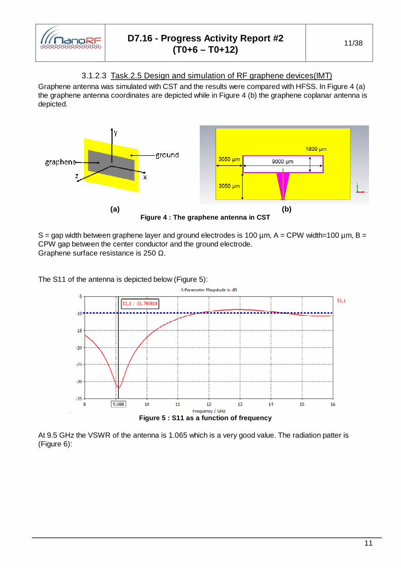
3.1.2.3 Task.2.5 Design and simulation of RF graphene devices(IMT) Graphene antenna was simulated with CST and the results were compared with HFSS. In Figure 4 (a) the graphene antenna coordinates are depicted while in Figure 4 (b) the graphene coplanar antenna is depicted.
(a) (b)
Figure 4 : The graphene antenna in CST
S = gap width between graphene layer and ground electrodes is 100 µm, A = CPW width=100 µm, B = CPW gap between the center conductor and the ground electrode. Graphene surface resistance is 250 Ω. The S11 of the antenna is depicted below (Figure 5):
Figure 5 : S11 as a function of frequency
At 9.5 GHz the VSWR of the antenna is 1.065 which is a very good value. The radiation patter is (Figure 6):
D7.16 - Progress Activity Report #2 (T0+6 – T0+12)
12/38
12
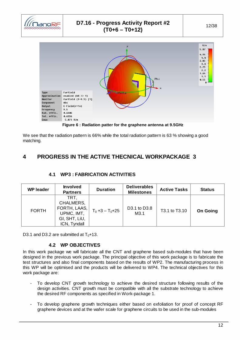
Figure 6 : Radiation patter for the graphene antenn a at 9.5GHz
We see that the radiation pattern is 66% while the total radiation pattern is 63 % showing a good matching.
4 PROGRESS IN THE ACTIVE THECNICAL WORKPACKAGE 3
4.1 WP3 : FABRICATION ACTIVITIES
WP leader Involved Partners
Duration Deliverables Milestones
Active Tasks Status
FORTH
TRT, CHALMERS,
FORTH, LAAS, UPMC, IMT, GI, SHT, LiU, ICN, Tyndall
T0 +3 – T0+25 D3.1 to D3.8 M3.1
T3.1 to T3.10 On Going
D3.1 and D3.2 are submitted at T0+13.
4.2 WP OBJECTIVES In this work package we will fabricate all the CNT and graphene based sub-modules that have been designed in the previous work package. The principal objective of this work package is to fabricate the test structures and also final components based on the results of WP2. The manufacturing process in this WP will be optimised and the products will be delivered to WP4. The technical objectives for this work package are:
- To develop CNT growth technology to achieve the desired structure following results of the design activities. CNT growth must be compatible with all the substrate technology to achieve the desired RF components as specified in Work-package 1.
- To develop graphene growth techniques either based on exfoliation for proof of concept RF graphene devices and at the wafer scale for graphene circuits to be used in the sub-modules

D7.16 - Progress Activity Report #2 (T0+6 – T0+12)
13/38
13
- To set-up a pilot line for manufacturing CNT for microwave applications.
- To fully characterize the CNT that have been grown by thermal CVD or plasma enhanced CVD . The characterization of graphene via exfoliation or epitaxial growth on SiC. The goal will be to verify that physical, structural, etc. properties will be compatible with the RF functions we want to achieve.
- To fabricate the RF submodules designed in the previous work package: CNT FET (LNA, PA and mixer), the RF switch, the RF filter/oscillator and the antenna, LNA based on graphene, graphene antenna , graphene mixer and graphene detector
- To develop various technologies that will allow for the integration of the sub-modules produced within this work package to be integrated on a single Si carrier wafer.
- To supply other work packages with CNT and graphene for characterization, modeling, simulation and demonstration and to optimize CNT and graphene according to their feedbacks.
4.2.1 PROGRESS TOWARD OBJECTIVES : STATUS OF ACTIVE S TASKS
4.2.1.1 Task.3.1 CNT and graphene growth technology
CNT growth (SHT/TRT) Several 5x5 mm² samples have been carried out in order to test different CNTs growth conditions. Catalyst dots of 1 µm and 250 nm diameter have been made on each of these samples. Regarding the CNTs diameter, single CNT is expected to grown on the 250 nm diameter catalyst dots whereas several CNTs are expected for a 1µm diameter catalyst dots. With this process developed at TRT, we can locate the CNT growth on the substrate. The process developed at TRT for the fabrication of CNTs catalyst dots is shown Figure 7(a). We remind the different steps:
Step A: deposition of the electronic resist by spin coating. Step B: definition of the catalyst dots diameter opening in the resist after an e-beam lithography
and resist development. Step C: using the resist as a mask, etching of second resist layer by a chemical etching in order
to make a bi-layer preventing a metallic stains to appear around the plot during the lift-off Figure 7(b).
Step D and E: deposition of the TiN as a diffusion layer and of the catalyst as for example Ni. Step F : removing the resist after a lift-off, we get a catalyst dots as shown in SEM picture on
Figure 8.
D7.16 - Progress Activity Report #2 (T0+6 – T0+12)
14/38
14
(a) (b)
Figure 7 : (a) Process flow for the TiN/Ni catalyst dots fabrication; (b) SEM picture of the 1µm bilay er resist before TiN/Ni deposition
CNTs growth is performed on this sample by SHT and the result are shown in Figure 8
Figure 8 : 1µm and 250nm TiN/Ni catalyst dots and C NT growth performed by SHT on this sample
D7.16 - Progress Activity Report #2 (T0+6 – T0+12)
15/38
15
Graphene growth There are several ways to obtain graphene material and we started to study the different graphene synthesis methods.
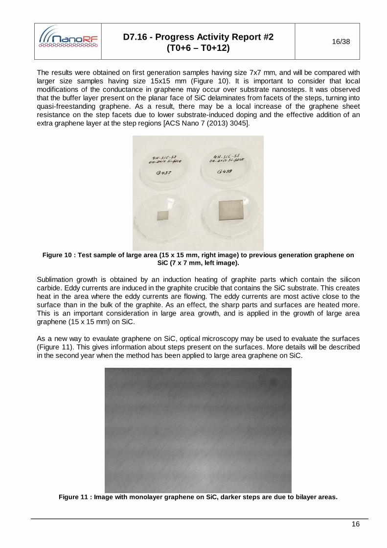
Graphene CVD growth on metals (SHT/CHALMERS) During this periode, graphene is grown by CVD method. Using Cu as catalyst, high quality of graphene films with different number of layers are obtained, as shown in Figure 9 below. SEM, TEM and Raman spectroscopy are used to evaluate the quality of the graphene material.
Figure 9 : Graphene film grown by CVD method and Ra man mapping shows high quality of mono-layer graphene
SiC decomposition (LiU) The graphene on silicon carbide has focused on thermal simulation and growth of monolayer graphene on large area substrates, evaluation of sheet resistance and a fast, simple and useful tool for evaluation of surface condition for graphene layers. Measuring the mobility generally requires patterning of the films and making electrical contact. The carrier density is needed to tune by a gate voltage. A recent non-contacting method has been used for measurement of the microwave surface impedance (conductivity) and sheet resistance of graphene thin films [arXiv:1304.1304]. The Table 1 compares sheet resistance, and demonstrates promising values for graphene on silicon carbide.
Table 1 : Sheet resistance for graphene on silicon carbide
D7.16 - Progress Activity Report #2 (T0+6 – T0+12)
16/38
16
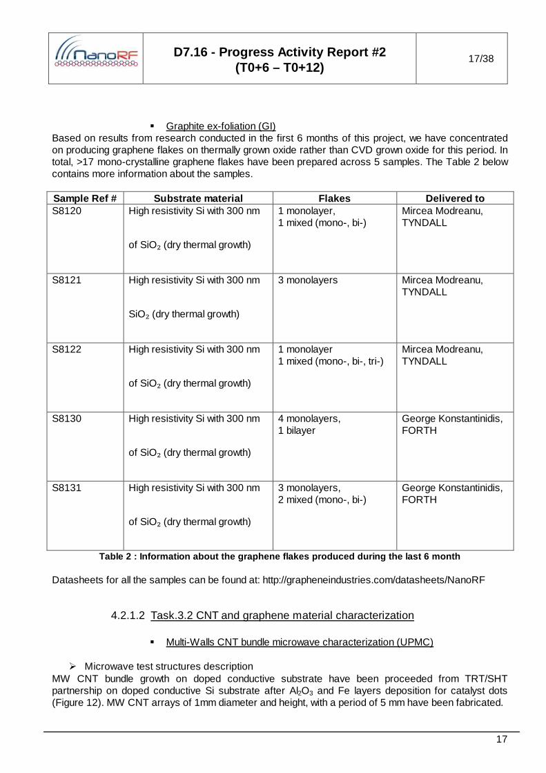
The results were obtained on first generation samples having size 7x7 mm, and will be compared with larger size samples having size 15x15 mm (Figure 10). It is important to consider that local modifications of the conductance in graphene may occur over substrate nanosteps. It was observed that the buffer layer present on the planar face of SiC delaminates from facets of the steps, turning into quasi-freestanding graphene. As a result, there may be a local increase of the graphene sheet resistance on the step facets due to lower substrate-induced doping and the effective addition of an extra graphene layer at the step regions [ACS Nano 7 (2013) 3045].
Figure 10 : Test sample of large area (15 x 15 mm, right image) to previous generation graphene on
SiC (7 x 7 mm, left image). Sublimation growth is obtained by an induction heating of graphite parts which contain the silicon carbide. Eddy currents are induced in the graphite crucible that contains the SiC substrate. This creates heat in the area where the eddy currents are flowing. The eddy currents are most active close to the surface than in the bulk of the graphite. As an effect, the sharp parts and surfaces are heated more. This is an important consideration in large area growth, and is applied in the growth of large area graphene (15 x 15 mm) on SiC. As a new way to evaulate graphene on SiC, optical microscopy may be used to evaluate the surfaces (Figure 11). This gives information about steps present on the surfaces. More details will be described in the second year when the method has been applied to large area graphene on SiC.
Figure 11 : Image with monolayer graphene on SiC, d arker steps are due to bilayer areas.
D7.16 - Progress Activity Report #2 (T0+6 – T0+12)
17/38
17
Graphite ex-foliation (GI) Based on results from research conducted in the first 6 months of this project, we have concentrated on producing graphene flakes on thermally grown oxide rather than CVD grown oxide for this period. In total, >17 mono-crystalline graphene flakes have been prepared across 5 samples. The Table 2 below contains more information about the samples. Sample Ref # Substrate material Flakes Delivered to S8120 High resistivity Si with 300 nm
of SiO₂ (dry thermal growth)
1 monolayer, 1 mixed (mono-, bi-)
Mircea Modreanu, TYNDALL
S8121 High resistivity Si with 300 nm
SiO₂ (dry thermal growth)
3 monolayers Mircea Modreanu, TYNDALL
S8122 High resistivity Si with 300 nm
of SiO₂ (dry thermal growth)
1 monolayer 1 mixed (mono-, bi-, tri-)
Mircea Modreanu, TYNDALL
S8130 High resistivity Si with 300 nm
of SiO₂ (dry thermal growth)
4 monolayers, 1 bilayer
George Konstantinidis, FORTH
S8131 High resistivity Si with 300 nm
of SiO₂ (dry thermal growth)
3 monolayers, 2 mixed (mono-, bi-)
George Konstantinidis, FORTH
Table 2 : Information about the graphene flakes pro duced during the last 6 month Datasheets for all the samples can be found at: http://grapheneindustries.com/datasheets/NanoRF
4.2.1.2 Task.3.2 CNT and graphene material characterization
Multi-Walls CNT bundle microwave characterization (UPMC)
Microwave test structures description MW CNT bundle growth on doped conductive substrate have been proceeded from TRT/SHT partnership on doped conductive Si substrate after Al2O3 and Fe layers deposition for catalyst dots (Figure 12). MW CNT arrays of 1mm diameter and height, with a period of 5 mm have been fabricated.
D7.16 - Progress Activity Report #2 (T0+6 – T0+12)
18/38
18
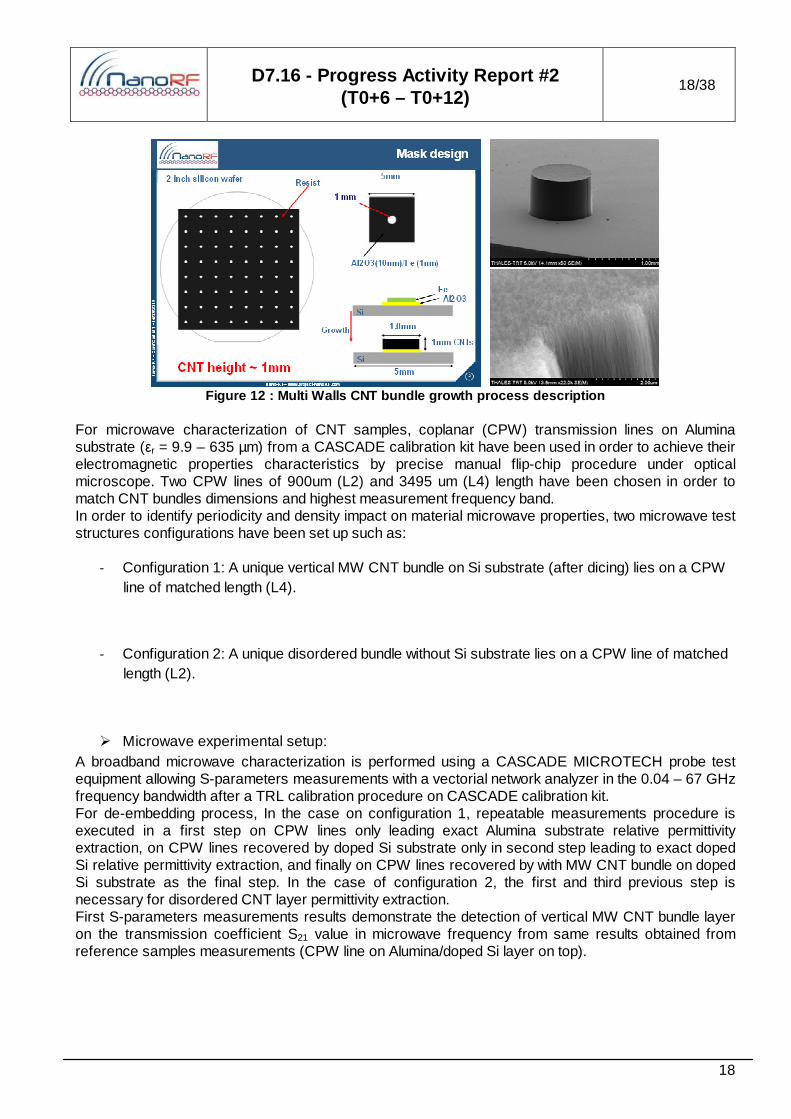
Figure 12 : Multi Walls CNT bundle growth process d escription
For microwave characterization of CNT samples, coplanar (CPW) transmission lines on Alumina substrate (εr = 9.9 – 635 µm) from a CASCADE calibration kit have been used in order to achieve their electromagnetic properties characteristics by precise manual flip-chip procedure under optical microscope. Two CPW lines of 900um (L2) and 3495 um (L4) length have been chosen in order to match CNT bundles dimensions and highest measurement frequency band. In order to identify periodicity and density impact on material microwave properties, two microwave test structures configurations have been set up such as:
- Configuration 1: A unique vertical MW CNT bundle on Si substrate (after dicing) lies on a CPW line of matched length (L4).
- Configuration 2: A unique disordered bundle without Si substrate lies on a CPW line of matched length (L2).
Microwave experimental setup: A broadband microwave characterization is performed using a CASCADE MICROTECH probe test equipment allowing S-parameters measurements with a vectorial network analyzer in the 0.04 – 67 GHz frequency bandwidth after a TRL calibration procedure on CASCADE calibration kit. For de-embedding process, In the case on configuration 1, repeatable measurements procedure is executed in a first step on CPW lines only leading exact Alumina substrate relative permittivity extraction, on CPW lines recovered by doped Si substrate only in second step leading to exact doped Si relative permittivity extraction, and finally on CPW lines recovered by with MW CNT bundle on doped Si substrate as the final step. In the case of configuration 2, the first and third previous step is necessary for disordered CNT layer permittivity extraction. First S-parameters measurements results demonstrate the detection of vertical MW CNT bundle layer on the transmission coefficient S21 value in microwave frequency from same results obtained from reference samples measurements (CPW line on Alumina/doped Si layer on top).

D7.16 - Progress Activity Report #2 (T0+6 – T0+12)
19/38
19
De-embedding procedures supported by electromagnetic simulations of multilayered structures are under work in order to apply analytical model described in [1,2] for final material relative permittivity extraction.
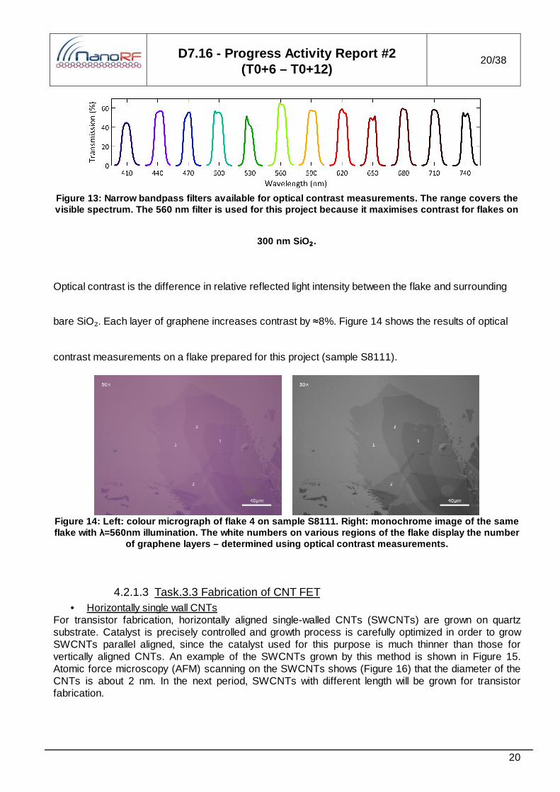
Graphene characterization (Tyndall, GI) Micro-Raman characterization of 7 different graphene samples was conducted. The samples were produced or acquired from graphene industries, LIU, SHT, and graphene supermarket and delivered by FORTH. Exfoliated graphene was transferred to Cu and SiO2 substrates. CVD graphene was grown on SiC substrates. Micro-Raman scattering measurements were performed on all samples. Based on the detailed analysis of the line shape, line width, intensity ratio and spectral position, all graphene samples were characterized and detailed information regarding defects, strain, doping and number of layers were obtained. The detailed results of these measurements are described in deliverable D3.2. A novel experimental method (two-colour Raman thermometry) was planned, developed and constructed. This method allows for the investigation of the thermal conductivity in CNTs and graphene as well as the determination of the heat transport regime. The potential of this technique was successfully demonstrated at ICN by showing different heat transport mechanism in ultra-thin Si membranes. The technique is capable of delivering line scans and two dimensional maps of the spatial temperature distribution around a power tuneable heating laser. The setup is currently used to measure the heat transport and thermal conductivity in graphene. All graphene flakes prepared by Graphene Industries are characterized using optical contrast. This is a fast and inexpensive method for determining the exact number of graphene layers in a flake. The method is described in the paper ‘Making graphene visible’ by Blake et al. (APL 2007).
Graphene flakes on oxidized silicon substrates with 300 nm of SiO₂ have a peak optical contrast at 560
nm, so we take images of flakes illuminated with light filtered to that wavelength to maximize the signal to noise ratio. We use narrow bandpass filters with a bandwidth of 10 nm. Figure 13 shows the range of filters we have available for characterizing flakes on a wide range of substrates.
[1] H. Kassem, V. Vigneras and G. Lunet , Characterization Techniques for Materials’ Properties Measurement, Microwave and
Millimeter Wave Technologies from Photonic Bandgap Devices to Antenna and Applications, Igor Minin (Ed.), ISBN: 978-953-7619-66-
4, 2010
[2] C. Veyres and V. Fouad Hanna, “Extension of the application of conformal mapping techniques to coplanar lines with finite
dimensions,” Int. J. Electron., vol. 48, pp. 47–56, 1980
D7.16 - Progress Activity Report #2 (T0+6 – T0+12)
20/38
20
Figure 13: Narrow bandpass filters available for op tical contrast measurements. The range covers the visible spectrum. The 560 nm filter is used for thi s project because it maximises contrast for flakes on
300 nm SiO ₂₂₂₂.
Optical contrast is the difference in relative reflected light intensity between the flake and surrounding
bare SiO₂. Each layer of graphene increases contrast by ≈8%. Figure 14 shows the results of optical
contrast measurements on a flake prepared for this project (sample S8111).
Figure 14: Left: colour micrograph of flake 4 on sa mple S8111. Right: monochrome image of the same flake with λ=560nm illumination. The white numbers on various r egions of the flake display the number
of graphene layers – determined using optical contr ast measurements.
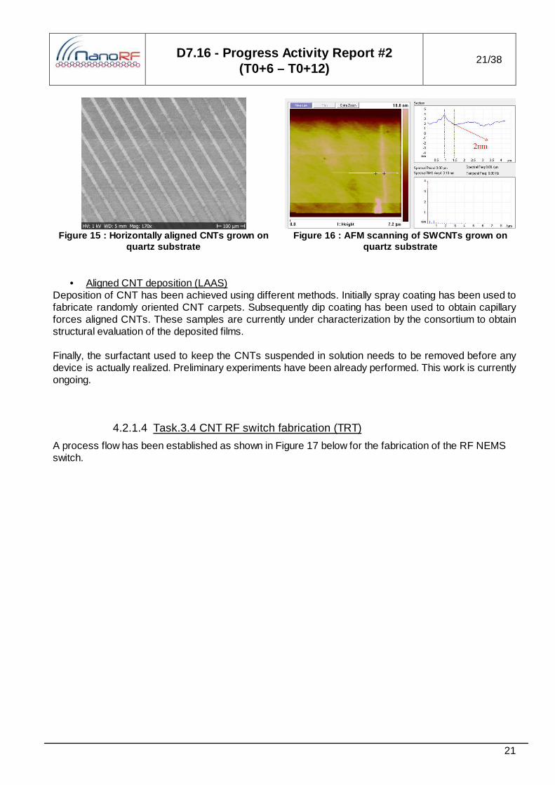
4.2.1.3 Task.3.3 Fabrication of CNT FET • Horizontally single wall CNTs
For transistor fabrication, horizontally aligned single-walled CNTs (SWCNTs) are grown on quartz substrate. Catalyst is precisely controlled and growth process is carefully optimized in order to grow SWCNTs parallel aligned, since the catalyst used for this purpose is much thinner than those for vertically aligned CNTs. An example of the SWCNTs grown by this method is shown in Figure 15. Atomic force microscopy (AFM) scanning on the SWCNTs shows (Figure 16) that the diameter of the CNTs is about 2 nm. In the next period, SWCNTs with different length will be grown for transistor fabrication.
D7.16 - Progress Activity Report #2 (T0+6 – T0+12)
21/38
21
Figure 15 : Horizontally aligned CNTs grown on
quartz substrate Figure 16 : AFM scanning of SWCNTs grown on
quartz substrate
• Aligned CNT deposition (LAAS) Deposition of CNT has been achieved using different methods. Initially spray coating has been used to fabricate randomly oriented CNT carpets. Subsequently dip coating has been used to obtain capillary forces aligned CNTs. These samples are currently under characterization by the consortium to obtain structural evaluation of the deposited films. Finally, the surfactant used to keep the CNTs suspended in solution needs to be removed before any device is actually realized. Preliminary experiments have been already performed. This work is currently ongoing.
4.2.1.4 Task.3.4 CNT RF switch fabrication (TRT)
A process flow has been established as shown in Figure 17 below for the fabrication of the RF NEMS switch.

D7.16 - Progress Activity Report #2 (T0+6 – T0+12)
22/38
22
Figure 17 : Process flow for the RF NEMS switch
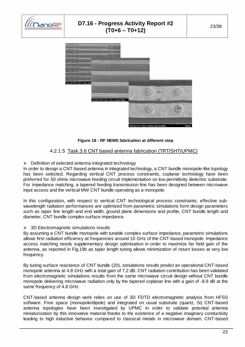
Figure 18 presents SEM pictures at different step of the fabrication process. Today, the fabrication is in progress.
D7.16 - Progress Activity Report #2 (T0+6 – T0+12)
23/38
23
Figure 18 : RF NEMS fabrication at different step
4.2.1.5 Task.3.6 CNT based antenna fabrication (TRT/SHT/UPMC) Definition of selected antenna integrated technology In order to design a CNT-based antenna in integrated technology, a CNT bundle monopole-like topology has been selected. Regarding vertical CNT process constraints, coplanar technology have been preferred for 50 ohms microwave feeding circuit implementation on low permittivity dielectric substrate. For impedance matching, a tapered feeding transmission line has been designed between microwave input access and the vertical MW CNT bundle operating as a monopole. In this configuration, with respect to vertical CNT technological process constraints, effective sub-wavelength radiation performances are optimized from parametric simulations form design parameters such as taper line length and end width, ground plane dimensions and profile, CNT bundle length and diameter, CNT bundle complex surface impedance. 3D Electromagnetic simulations results By assuming a CNT bundle monopole with tunable complex surface impedance, parametric simulations allows first radiation efficiency at frequencies around 10 GHz of the CNT-based monopole. Impedance access matching needs supplementary design optimization in order to maximize far field gain of the antenna, as reported in Fig.19b as taper length tuning allows minimization of return losses at very low frequency. By tuning surface reactance of CNT bundle (20), simulations results predict an operational CNT-based monopole antenna at 4.8 GHz with a total gain of 7.2 dB. CNT radiation contribution has been validated from electromagnetic simulations results from the same microwave circuit design without CNT bundle monopole delivering microwave radiation only by the tapered coplanar line with a gain of -8.9 dB at the same frequency of 4.8 GHz. CNT-based antenna design work relies on use of 3D FDTD electromagnetic analysis from HFSS software. Free space (monopole/dipole) and integrated on usual substrate (quartz, Si) CNT-based antenna topologies have been investigated by UPMC in order to validate potential antenna miniaturization by this innovative material thanks to the existence of a negative imaginary conductivity leading to high inductive behavior compared to classical metals in microwave domain. CNT-based
D7.16 - Progress Activity Report #2 (T0+6 – T0+12)
24/38
24
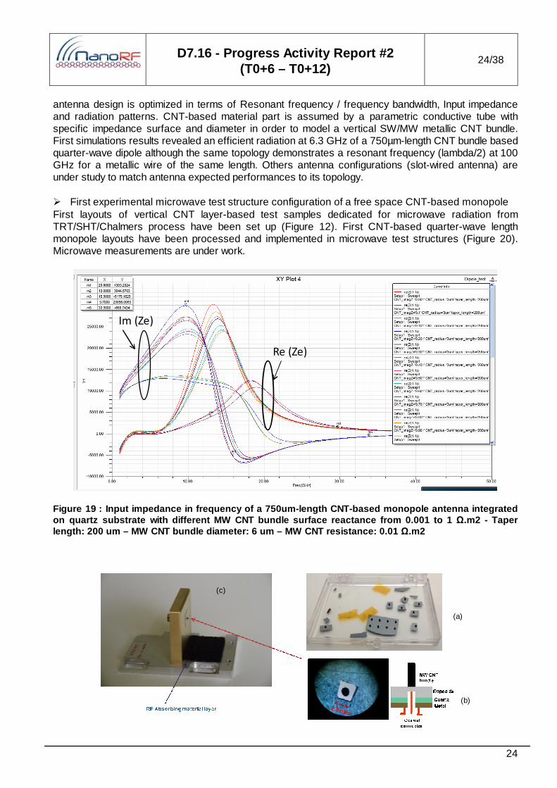
antenna design is optimized in terms of Resonant frequency / frequency bandwidth, Input impedance and radiation patterns. CNT-based material part is assumed by a parametric conductive tube with specific impedance surface and diameter in order to model a vertical SW/MW metallic CNT bundle. First simulations results revealed an efficient radiation at 6.3 GHz of a 750µm-length CNT bundle based quarter-wave dipole although the same topology demonstrates a resonant frequency (lambda/2) at 100 GHz for a metallic wire of the same length. Others antenna configurations (slot-wired antenna) are under study to match antenna expected performances to its topology. First experimental microwave test structure configuration of a free space CNT-based monopole First layouts of vertical CNT layer-based test samples dedicated for microwave radiation from TRT/SHT/Chalmers process have been set up (Figure 12). First CNT-based quarter-wave length monopole layouts have been processed and implemented in microwave test structures (Figure 20). Microwave measurements are under work.
Im (Ze)
Re (Ze)
Figure 19 : Input impedance in frequency of a 750um -length CNT-based monopole antenna integrated on quartz substrate with different MW CNT bundle su rface reactance from 0.001 to 1 Ω.m2 - Taper length: 200 um – MW CNT bundle diameter: 6 um – MW CNT resistance: 0.01 Ω.m2
(a)
(b)
(c)
D7.16 - Progress Activity Report #2 (T0+6 – T0+12)
25/38
25
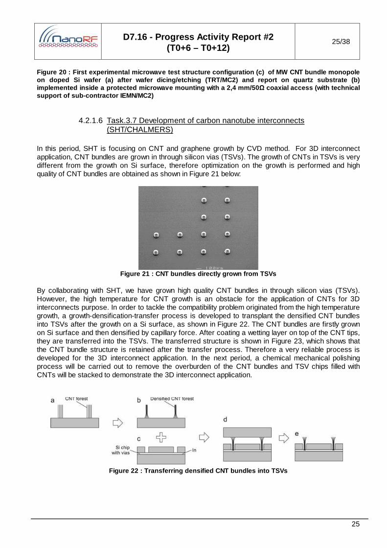
Figure 20 : First experimental microwave test struc ture configuration (c) of MW CNT bundle monopole on doped Si wafer (a) after wafer dicing/etching (T RT/MC2) and report on quartz substrate (b) implemented inside a protected microwave mounting w ith a 2,4 mm/50 Ω coaxial access (with technical support of sub-contractor IEMN/MC2)
4.2.1.6 Task.3.7 Development of carbon nanotube interconnects (SHT/CHALMERS)
In this period, SHT is focusing on CNT and graphene growth by CVD method. For 3D interconnect application, CNT bundles are grown in through silicon vias (TSVs). The growth of CNTs in TSVs is very different from the growth on Si surface, therefore optimization on the growth is performed and high quality of CNT bundles are obtained as shown in Figure 21 below:
Figure 21 : CNT bundles directly grown from TSVs
By collaborating with SHT, we have grown high quality CNT bundles in through silicon vias (TSVs). However, the high temperature for CNT growth is an obstacle for the application of CNTs for 3D interconnects purpose. In order to tackle the compatibility problem originated from the high temperature growth, a growth-densification-transfer process is developed to transplant the densified CNT bundles into TSVs after the growth on a Si surface, as shown in Figure 22. The CNT bundles are firstly grown on Si surface and then densified by capillary force. After coating a wetting layer on top of the CNT tips, they are transferred into the TSVs. The transferred structure is shown in Figure 23, which shows that the CNT bundle structure is retained after the transfer process. Therefore a very reliable process is developed for the 3D interconnect application. In the next period, a chemical mechanical polishing process will be carried out to remove the overburden of the CNT bundles and TSV chips filled with CNTs will be stacked to demonstrate the 3D interconnect application.
Figure 22 : Transferring densified CNT bundles into TSVs
D7.16 - Progress Activity Report #2 (T0+6 – T0+12)
26/38
26
Figure 23 : Transferring densified CNT bundles into TSV structure
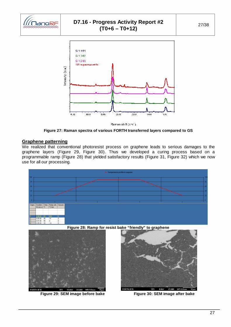
4.2.1.7 Task.3.8 Development of RF graphene devices Graphene Transfer FORTH is developing its own graphene transfer technology. Initially the transfer was performed on silicon dioxide. The qualities of the transferred layers were characterized by Raman (Figure 27). The Raman analysis does not show significant difference between the GS (graphene supermarket) and FORTH transferred graphene layers. FORTH has also developed contact technology. Thus TLM patterns using Palladium and Gold contacts on transferred (Figure 25) and supermarket graphene (Figure 24) were fabricated and the quality of the contacts was compared (Figure 26). It is evident that the results are very similar thus it is an additional confirmation that the transfer process of FORTH leads to good quality graphene layers. FORTH is currently transferring graphene to other substrates with similar crystallographic properties to that of graphene in order to investigate the effect of the substrate onto the mobility of the grapheme layers.
Figure 24: TLM on GS material
Figure 25: TLM on FORTH transfer
Figure 26: Comparison of contacts
D7.16 - Progress Activity Report #2 (T0+6 – T0+12)
27/38
27
Figure 27: Raman spectra of various FORTH transferr ed layers compared to GS
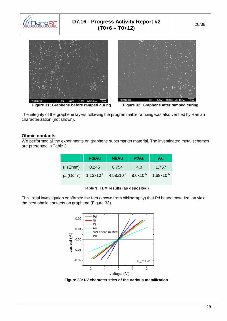
Graphene patterning We realized that conventional photoresist process on graphene leads to serious damages to the graphene layers (Figure 29, Figure 30). Thus we developed a curing process based on a programmable ramp (Figure 28) that yielded satisfactory results (Figure 31, Figure 32) which we now use for all our processing.
Figure 28: Ramp for resist bake “friendly” to graph ene
Figure 29: SEM image before bake Figure 30: SEM ima ge after bake
D7.16 - Progress Activity Report #2 (T0+6 – T0+12)
28/38
28
Figure 31: Graphene before ramped curing Figure 32: Graphene after ramped curing
The integrity of the graphene layers following the programmable ramping was also verified by Raman characterization (not shown). Ohmic contacts We performed all the experiments on graphene supermarket material. The investigated metal schemes are presented in Table 3
Pd/Au Ni/Au Pt/Au Au
rt (Ωmm) 0.245 0.754 4.0 1.757
ρc (Ωcm2) 1.13x10⁻⁶ 4.58x10⁻⁶ 8.6x10⁻⁵ 1.68x10⁻⁵
Table 3: TLM results (as deposited) This initial investigation confirmed the fact (known from bibliography) that Pd based metallization yield the best ohmic contacts on graphene (Figure 33).
Figure 33: I-V characteristics of the various metal lization

D7.16 - Progress Activity Report #2 (T0+6 – T0+12)
29/38
29
Based on a new idea, we have developed a metal contact based on two materials X and Y and annealing (not common for graphene) (we see patent possibility thus not reporting details at this stage) which yielded the following very promising results (Table 3, Figure 34): Rc (Ω) Rsh (Ω/sq) ρc (Ω cm2) 300 (best) 0.757 1,514 6.49x10⁻⁷ 300 (mean) 2.88 1,508 3.44x10⁻⁶ 350 5.05 1,715 9.2x10⁻⁶
Table 4 : TLM results of contact X-Y on GS graphene with binary
Figure 34 : TLM results comparison
An interesting finding was that X becomes ohmic (significantly inferior to the binary though) upon annealing, while Y does not become ohmic at all. We performed a second experiment on a different sample to verify the very low contact resistance but the results were as not as good as in the 1st run. Thus this is an ongoing investigation. Dielectrics During the reporting period we investigated different dielectics for the graphene devices fabrication
o Parylene coatings (LAAS/Tyndall) Parylene is a vacuum deposited polymer whith room temperature deposition temperature. Due to its molecular structure Parylene has been identified as a potential dielectric which may be “graphene compatible” in the sense tha tit causes minimum mobility degradation. Furthermore, Parylene can be deposited in very thin layer in a very controllable manner which makes it promising as a low cost gate dielectric material. CNRS – LAAS has optimized the deposition of Parylene – N and, in collaboration with FORTH, a GFET run was realized. Although Parylene has successfully isolated the gate electrode, reliability issues have been identified during electrical characterization of the resulting devices. The reason for this is under investigation but possibly Parylene-N is not stable enough to act as a gate electrode. Tyndall also developed an in-house process for 90nm-thick Parylene N thin films as Parylene N/metal high-k metal oxide stack is currently selected as an option for gate oxides for graphene and CNT FET devices that will be developed in Task 3.3 and Task 3.8. During the next period Tyndall intends to explore the possibility of scaling down the Parylene N thin film thickness down to 25nm.
D7.16 - Progress Activity Report #2 (T0+6 – T0+12)
30/38
30
The dispersion of the optical constants and the Raman spectrum for 90nm-thick Parylene N thin film are shown in Figure 35 and Figure 36 below.
Figure 35 : The optical constant dispersion for 90nm-thick Parylene N thin film
Figure 36 : The Raman spectrum of 90nm-thick Parylene N thin film
o Thin Polyimide layers (LAAS) Polyimide is routinely used in conventional processing as an interlayer dielectric. It is an especially stable material (Thermally stable up to more than 400C) and can be applied by spin coating which facilitates its application on graphene. Its properties have been identified as favorable for graphene interfacing. CNRS – LAAS has worked on reducing the Polyimide final film thickness below 100nm. Currently 200nm or less can be fabricated repeatably.
o ZrO 2 and HfO 2 (Tyndall/ICN) We had continued the work for developing a room temperature e-beam process for the growth of high-k metal oxides (ZrO2 and HfO2) suitable as gate oxides for graphene and CNT FET devices that will be developed in Task 3.3 and Task 3.8. Three samples grown by e-beam in Tyndall on Si substrates, 2 HfO2 thin films and one ZrO2 thin film have been sending to ICN for thermal conductivity measurements by 3 omega technique. ICN has performed thermal conductivity measurements of these materials using a home-built experiment based on the 3 omega measurement technique. The setup allows measurements at sample temperature between 5 K and more than 400 K using a wide frequency range between 1 Hz and 10 kHz and excitation currents between 2 nA and 100 mA. The cross-plane thermal conductivity at room temperature was determined to 0.88 W/mK for ZrO2 and 0.65 W/mK for HfO2. The temperature dependence of the thermal conductivity confirms the amorphous character of the material. The obtained results constitute important input parameters for the fabrication and optimization of the CNT and graphene based filters, FETs, switches, antennas, and interconnects in D3.3 – D3.7.
o Silicon Nitride We developed a very low power process. Raman analysis (Figure 37) shows that the graphene layer exists while TLM analysis shows a graphene layer but with inferior performance to the uncovered graphene. This is ongoing investigation.
1000 1250 1500 1750 2000 2250 2500 2750 3000 32500
200
400
600
800
1000
1200
1400
1600
1800
Inte
nsity
(co
unts
)
Raman shifts(cm-1)
Parylene N, 90-nm thick
D7.16 - Progress Activity Report #2 (T0+6 – T0+12)
31/38
31
Figure 37: Raman analysis of SiN encapsulated graph ene
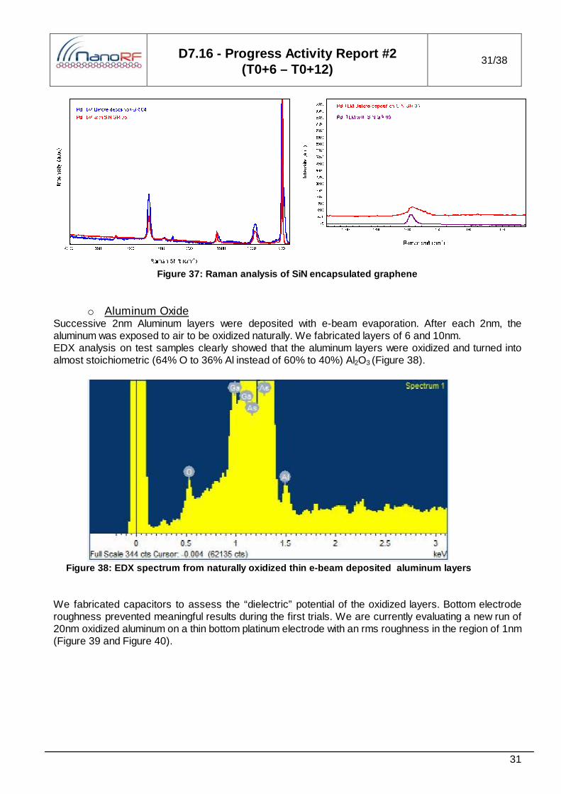
o Aluminum Oxide Successive 2nm Aluminum layers were deposited with e-beam evaporation. After each 2nm, the aluminum was exposed to air to be oxidized naturally. We fabricated layers of 6 and 10nm. EDX analysis on test samples clearly showed that the aluminum layers were oxidized and turned into almost stoichiometric (64% O to 36% Al instead of 60% to 40%) Al2O3 (Figure 38).
Figure 38: EDX spectrum from naturally oxidized thi n e-beam deposited aluminum layers
We fabricated capacitors to assess the “dielectric” potential of the oxidized layers. Bottom electrode roughness prevented meaningful results during the first trials. We are currently evaluating a new run of 20nm oxidized aluminum on a thin bottom platinum electrode with an rms roughness in the region of 1nm (Figure 39 and Figure 40).
D7.16 - Progress Activity Report #2 (T0+6 – T0+12)
32/38
32
Figure 39: AFM analysis of Pt bottom electrode of
the test capacitors Figure 40: Fabricated capacitor
Substrate optimization
Another issue that has been attacked during this period is the detrimental effect that processing has on graphene performance. Specifically there are two issues associated with conventional processing. First of all, graphene undergoes all processing steps until a complete circuit is fabricated. These results in reduced mobility due to contamination, an effect to which graphene is especially sensitive. Secondly, Silicon itself although used for high frequency circuits has only the role of mechanical support in carbon based circuits. In fact the RF losses associated with Silicon diminish the total circuit performance.
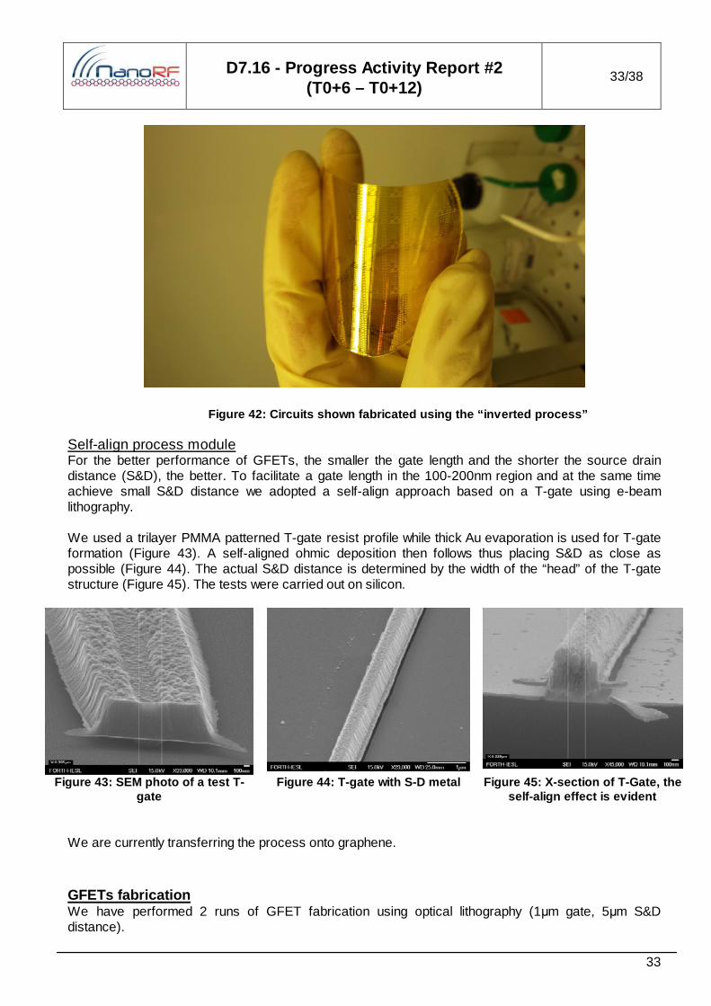
Figure 41: conventional (left) and inverted (right) processing concepts. The latter provides a low los s polymeric substrate and at the same time does not e xpose the sensitive graphene layer to any processing steps which reduces its contamination le vel. Using this concept, coplanar waveguide lines were fabricated and the substrate losses have been characterized. Especially for small lines the observed losses are significantly less. Finally graphene has been transferred on top of the lines and both an RF property as well as contacting with undelaying metallization has been verified.
This concept is now being used to fabricate FET devices for graphene as well as CNTs (Figure 42). An added bonus of this fabrication method is the fact that flexible circuits can be fabricated assuming the polymer used has good elastic properties.
D7.16 - Progress Activity Report #2 (T0+6 – T0+12)
33/38
33
Figure 42: Circuits shown fabricated using the “inv erted process”
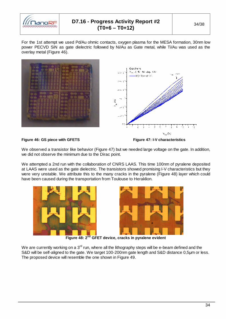
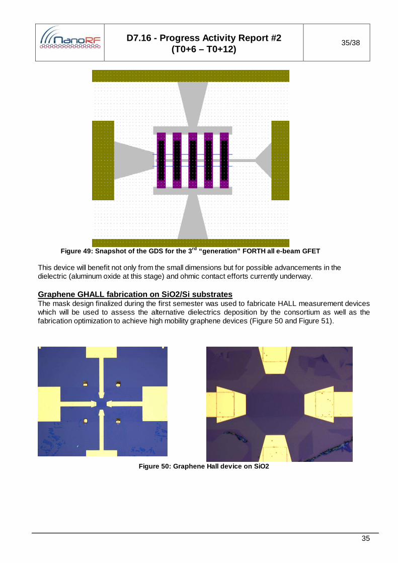
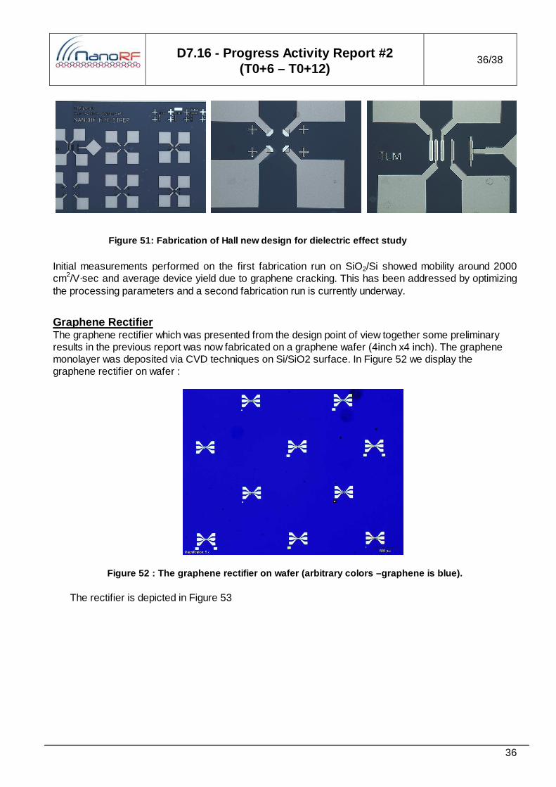
Self-align process module For the better performance of GFETs, the smaller the gate length and the shorter the source drain distance (S&D), the better. To facilitate a gate length in the 100-200nm region and at the same time achieve small S&D distance we adopted a self-align approach based on a T-gate using e-beam lithography. We used a trilayer PMMA patterned T-gate resist profile while thick Au evaporation is used for T-gate formation (Figure 43). A self-aligned ohmic deposition then follows thus placing S&D as close as possible (Figure 44). The actual S&D distance is determined by the width of the “head” of the T-gate structure (Figure 45). The tests were carried out on silicon.
Figure 43: SEM photo of a test T-
gate Figure 44: T-gate with S-D metal Figure 45: X-section of T-Gate, the
self-align effect is evident We are currently transferring the process onto graphene. GFETs fabrication We have performed 2 runs of GFET fabrication using optical lithography (1µm gate, 5µm S&D distance).
D7.16 - Progress Activity Report #2 (T0+6 – T0+12)
34/38
34
For the 1st attempt we used Pd/Au ohmic contacts, oxygen plasma for the MESA formation, 30nm low power PECVD SiN as gate dielectric followed by Ni/Au as Gate metal, while Ti/Au was used as the overlay metal (Figure 46).
Figure 46: GS piece with GFETS Figure 47: I-V characteristics We observed a transistor like behavior (Figure 47) but we needed large voltage on the gate. In addition, we did not observe the minimum due to the Dirac point. We attempted a 2nd run with the collaboration of CNRS LAAS. This time 100nm of pyralene deposited at LAAS were used as the gate dielectric. The transistors showed promising I-V characteristics but they were very unstable. We attribute this to the many cracks in the pyralene (Figure 48) layer which could have been caused during the transportation from Toulouse to Heraklion.
Figure 48: 2 nd GFET device, cracks in pyralene evident
We are currently working on a 3rd run, where all the lithography steps will be e-beam defined and the S&D will be self-aligned to the gate. We target 100-200nm gate length and S&D distance 0,5µm or less. The proposed device will resemble the one shown in Figure 49.
D7.16 - Progress Activity Report #2 (T0+6 – T0+12)
35/38
35
Figure 49: Snapshot of the GDS for the 3 rd “generation” FORTH all e-beam GFET
This device will benefit not only from the small dimensions but for possible advancements in the dielectric (aluminum oxide at this stage) and ohmic contact efforts currently underway. Graphene GHALL fabrication on SiO2/Si substrates The mask design finalized during the first semester was used to fabricate HALL measurement devices which will be used to assess the alternative dielectrics deposition by the consortium as well as the fabrication optimization to achieve high mobility graphene devices (Figure 50 and Figure 51).
Figure 50: Graphene Hall device on SiO2
D7.16 - Progress Activity Report #2 (T0+6 – T0+12)
36/38
36
Figure 51: Fabrication of Hall new design for diele ctric effect study
Initial measurements performed on the first fabrication run on SiO2/Si showed mobility around 2000 cm2/V·sec and average device yield due to graphene cracking. This has been addressed by optimizing the processing parameters and a second fabrication run is currently underway.
Graphene Rectifier The graphene rectifier which was presented from the design point of view together some preliminary results in the previous report was now fabricated on a graphene wafer (4inch x4 inch). The graphene monolayer was deposited via CVD techniques on Si/SiO2 surface. In Figure 52 we display the graphene rectifier on wafer :
Figure 52 : The graphene rectifier on wafer (arbitr ary colors –graphene is blue). The rectifier is depicted in Figure 53

D7.16 - Progress Activity Report #2 (T0+6 – T0+12)
37/38
37
Figure 53 : The graphene rectifier
In Figure 54 there is the photo of the graphene rectifier on wafer ready for measurement. The third electrode arm is the back-gate voltage.
Figure 54 : The graphene rectifier under measuremen t (Keithley 4200 SCS).
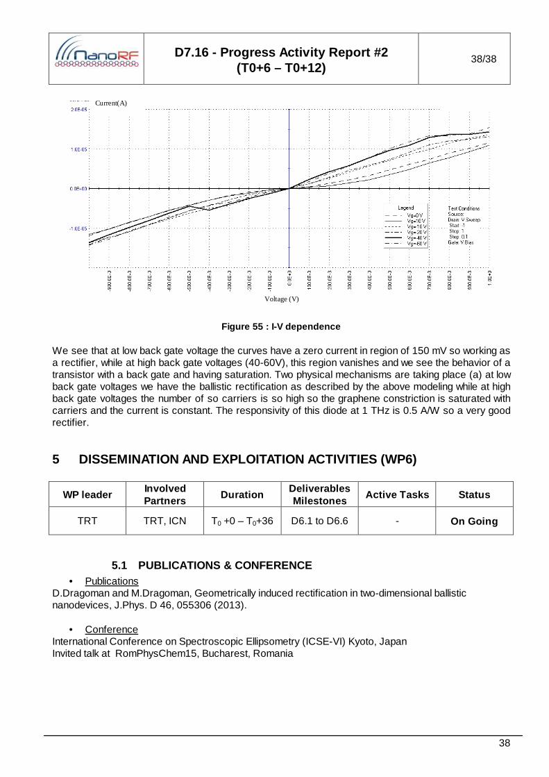
The I-V dependence is displayed in Figure 55
D7.16 - Progress Activity Report #2 (T0+6 – T0+12)
38/38
38
Voltage (V)
Current(A)
Figure 55 : I-V dependence
We see that at low back gate voltage the curves have a zero current in region of 150 mV so working as a rectifier, while at high back gate voltages (40-60V), this region vanishes and we see the behavior of a transistor with a back gate and having saturation. Two physical mechanisms are taking place (a) at low back gate voltages we have the ballistic rectification as described by the above modeling while at high back gate voltages the number of so carriers is so high so the graphene constriction is saturated with carriers and the current is constant. The responsivity of this diode at 1 THz is 0.5 A/W so a very good rectifier.
5 DISSEMINATION AND EXPLOITATION ACTIVITIES (WP6)
WP leader Involved Partners
Duration Deliverables Milestones
Active Tasks Status
TRT TRT, ICN T0 +0 – T0+36 D6.1 to D6.6 - On Going
5.1 PUBLICATIONS & CONFERENCE • Publications
D.Dragoman and M.Dragoman, Geometrically induced rectification in two-dimensional ballistic nanodevices, J.Phys. D 46, 055306 (2013).
• Conference International Conference on Spectroscopic Ellipsometry (ICSE-VI) Kyoto, Japan Invited talk at RomPhysChem15, Bucharest, Romania


