d22 Layout Implementation of Digital to Analog
70
qwertyuiopasdfghjklzxcvbnmqwerty uiopasdfghjklzxcvbnmqwertyuiopasd fghjklzxcvbnmqwertyuiopasdfghjklzx cvbnmqwertyuiopasdfghjklzxcvbnmq wertyuiopasdfghjklzxcvbnmqwertyui opasdfghjklzxcvbnmqwertyuiopasdfg hjklzxcvbnmqwertyuiopasdfghjklzxc vbnmqwertyuiopasdfghjklzxcvbnmq wertyuiopasdfghjklzxcvbnmqwertyui opasdfghjklzxcvbnmqwertyuiopasdfg hjklzxcvbnmqwertyuiopasdfghjklzxc vbnmqwertyuiopasdfghjklzxcvbnmq wertyuiopasdfghjklzxcvbnmqwertyui opasdfghjklzxcvbnmqwertyuiopasdfg hjklzxcvbnmrtyuiopasdfghjklzxcvbn mqwertyuiopasdfghjklzxcvbnmqwert yuiopasdfghjklzxcvbnmqwertyuiopas dfghjklzxcvbnmqwertyuiopasdfghjklz LAYOUT IMPLEMENTATION OF DIGITAL TO ANALOG www.BEProjectReport.com VISIT US, CHOOSE THE PROJECT YOU LIKE AND CLICK THE DOWNLOAD BUTTON
-
Upload
maheshsamanapally -
Category
Documents
-
view
50 -
download
5
description
read it
Transcript of d22 Layout Implementation of Digital to Analog

qwertyuiopasdfghjklzxcvbnmqwerty
uiopasdfghjklzxcvbnmqwertyuiopasd
fghjklzxcvbnmqwertyuiopasdfghjklzx
cvbnmqwertyuiopasdfghjklzxcvbnmq
wertyuiopasdfghjklzxcvbnmqwertyui
opasdfghjklzxcvbnmqwertyuiopasdfg
hjklzxcvbnmqwertyuiopasdfghjklzxc
vbnmqwertyuiopasdfghjklzxcvbnmq
wertyuiopasdfghjklzxcvbnmqwertyui
opasdfghjklzxcvbnmqwertyuiopasdfg
hjklzxcvbnmqwertyuiopasdfghjklzxc
vbnmqwertyuiopasdfghjklzxcvbnmq
wertyuiopasdfghjklzxcvbnmqwertyui
opasdfghjklzxcvbnmqwertyuiopasdfg
hjklzxcvbnmrtyuiopasdfghjklzxcvbn
mqwertyuiopasdfghjklzxcvbnmqwert
yuiopasdfghjklzxcvbnmqwertyuiopas
dfghjklzxcvbnmqwertyuiopasdfghjklz
LAYOUT IMPLEMENTATION OF
DIGITAL TO ANALOG
www.BEProjectReport.com
VISIT US, CHOOSE THE PROJECT YOU LIKE AND
CLICK THE DOWNLOAD BUTTON

LAYOUT IMPLEMENTATION OF DIGITAL TO ANALOG
www.BEProjectReport.com Page 2
CHAPTER 1
INTRODUCTION
INTRODUCTION TO INTEGRATED CIRCUIT LAYOUT(IC LAYOUT):
Integrated circuit layout, also known IC layout, IC mask layout, or mask design, is the
representation of an integrated circuit in terms of planar geometric shapes which correspond to the
patterns of metal, oxide, or semiconductor layers that make up the components of the integrated
circuit. It‘s nothing but Top View of the Cross-sectional Device.
When using a standard process - where the interaction of the many chemical, thermal, and
photographic variables are known and carefully controlled - the behavior of the final integrated
circuit depends largely on the positions and interconnections of the geometric shapes. A layout
engineer's job is to place and connect all the components that make up a chip so that they meet all
criteria. Typical goals are performance, size, and manufacturability.
The layout must pass a series of checks in a process known as verification; the two most
common checks in the verification process are Design Rule Checking (DRC), and Layout Versus
Schematic (LVS). When all verification is complete the data is translated into an industry standard
format, typically GDSII, and sent to a semiconductor foundry. The process of sending this data to the
foundry is called tape out, due to the fact the data used to be shipped out on a magnetic tape. The
foundry converts the data into another format and uses it to generate the photo masks used in a
photolithographic process of semiconductor device fabrication.
In the earlier, simpler, days of IC design, layout was done by hand using opaque tapes and
films, much like the early days of PCB design. Modern IC Layout is done with the aid of IC layout
editor software, or even automatically using EDA tools, including place and route tools or schematic
driven layout tools. The manual operation of choosing and positioning the geometric shapes is
informally known as "polygon pushing".

LAYOUT IMPLEMENTATION OF DIGITAL TO ANALOG
www.BEProjectReport.com Page 3
CHAPTER 2
SEMICONDUCTOR AND TECHNOLOGY
2.1 RELIABILITY OF SEMICONDUCTOR DEVICES
Semiconductor devices are very sensitive to impurities and particles. Therefore, to
manufacture these devices it is necessary to manage many processes while accurately controlling the
level of impurities and particles. The finished product quality depends upon the many layered
relationship of each interacting substance in the semiconductor, including metallization, chip
material (list of semiconductor materials) and package.
The problems of micro-processes, and thin films and must be fully understood as they apply
to metallization and bonding wire bonding. It is also necessary to analyze surface phenomena from
the aspect of thin films.
Due to the rapid advances in technology, many new devices are developed using new
materials and processes, and design calendar time is limited due to non-recurring engineering
constraints, plus time to market concerns. Consequently, it is not possible to base new designs on the
reliability of existing devices.
To achieve economy of scale, semiconductor products are manufactured in high volume.
Furthermore repair of finished semiconductor products is impractical. Therefore incorporation of
reliability at the design stage and reduction of variation in the production stage have become
essential.
Reliability of semiconductor devices may depend on assembly, use, and environmental
conditions. Stress factors effecting device reliability include gas, dust, contamination, voltage,
current density, temperature, humidity, mechanical stress, vibration, shock, radiation, pressure, and
intensity of magnetic and electrical fields.
Design factors affecting semiconductor reliability include: voltage derating, power derating,
current derating, metastability, logic timing margins (logic simulation), timing analysis, temperature
derating, and process control.
LAYOUT IMPLEMENTATION OF DIGITAL TO ANALOG
www.BEProjectReport.com Page 4
CHAPTER 3
DIGITAL VS ANALOG SYSTEMS
3.1 DIGITAL VS ANALOG SYSTEMS
Connecting digital circuitry to sensor devices is simple if the sensor devices are inherently
digital themselves. Switches, relays, and encoders are easily interfaced with gate circuits due to the
on/off nature of their signals. However, when analog devices are involved, interfacing becomes
much more complex. What is needed is a way to electronically translate analog signals into digital
(binary) quantities, and vice versa. An analog-to-digital converter, or ADC, performs the former task
while a digital-to-analog converter, or DAC, performs the latter.
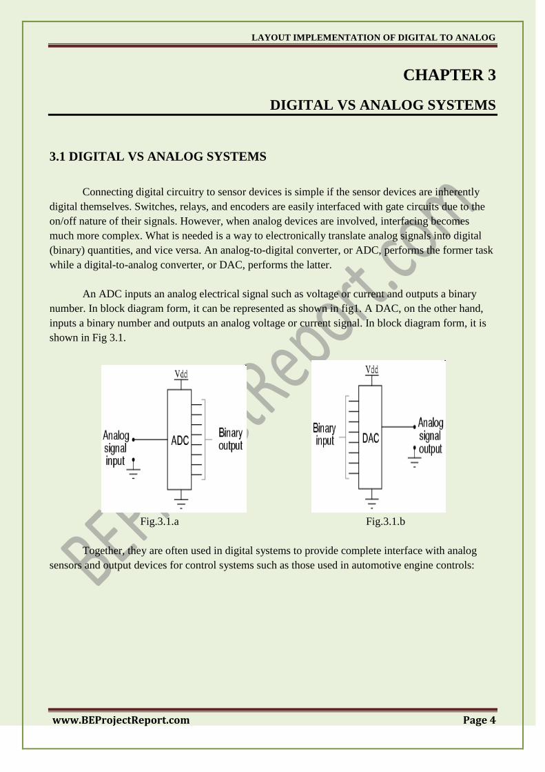
An ADC inputs an analog electrical signal such as voltage or current and outputs a binary
number. In block diagram form, it can be represented as shown in fig1. A DAC, on the other hand,
inputs a binary number and outputs an analog voltage or current signal. In block diagram form, it is
shown in Fig 3.1.
Fig.3.1.a Fig.3.1.b
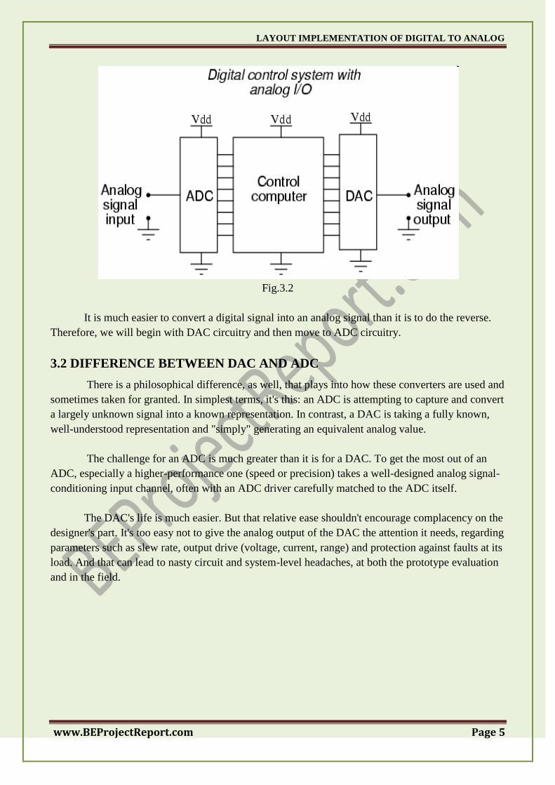
Together, they are often used in digital systems to provide complete interface with analog
sensors and output devices for control systems such as those used in automotive engine controls:
LAYOUT IMPLEMENTATION OF DIGITAL TO ANALOG
www.BEProjectReport.com Page 5
Fig.3.2
It is much easier to convert a digital signal into an analog signal than it is to do the reverse.
Therefore, we will begin with DAC circuitry and then move to ADC circuitry.
3.2 DIFFERENCE BETWEEN DAC AND ADC
There is a philosophical difference, as well, that plays into how these converters are used and
sometimes taken for granted. In simplest terms, it's this: an ADC is attempting to capture and convert
a largely unknown signal into a known representation. In contrast, a DAC is taking a fully known,
well-understood representation and "simply" generating an equivalent analog value.
The challenge for an ADC is much greater than it is for a DAC. To get the most out of an
ADC, especially a higher-performance one (speed or precision) takes a well-designed analog signal-
conditioning input channel, often with an ADC driver carefully matched to the ADC itself.
The DAC's life is much easier. But that relative ease shouldn't encourage complacency on the
designer's part. It's too easy not to give the analog output of the DAC the attention it needs, regarding
parameters such as slew rate, output drive (voltage, current, range) and protection against faults at its
load. And that can lead to nasty circuit and system-level headaches, at both the prototype evaluation
and in the field.
LAYOUT IMPLEMENTATION OF DIGITAL TO ANALOG
www.BEProjectReport.com Page 6
CHAPTER 4
ASIC & FULL CUSTOM VS SEMI CUSTOM
4.1 WHAT IS ASIC?
Any IC other than a general purpose IC which contains the functionality of thousands of gates is
usually called an ASIC (Application Specific Integrated Circuit). ASICs are designed to fit a certain
application. or A chip designed to perform a particular operation as opposed to General Purpose
integrated circuits
An ASIC is a digital or mixed-signal circuit designed to meet specifications set by a Specific project.
And it is NOT software programmable to perform different tasks.
4.1.1 General Purpose Integrated Circuits:
• Programmable microprocessors (e.g. Intel Pentium Series, Motorola HC-11)
Used in PCs to washing machines
• Programmable Digital Signal Processors (e.g. TI TMS 320 Series)
Used in many multimedia, sensor processing and communications applications
• Memory (DRAM, SRAM, etc.)
4.1.2 Examples of ASICs:
• Video processor to decode MPEG-2 digital TV signals
• Audio processor to perform Dolby AC3 encoding
• Low power DSP/controller for cell phone
4.2 ASIC DESIGN STYLES
Several design styles can be considered for chip implementation of specified algorithms or logic
functions. Each design style has its own merits and shortcomings, and thus a proper choice has to be
made by designers in order to provide the functionality at low cost.
They belong to two general cases
1 Full-custom layout approaches
2 Semi-custom layout approaches

LAYOUT IMPLEMENTATION OF DIGITAL TO ANALOG
www.BEProjectReport.com Page 7
4.2.1. Full-Custom Layout
Full-custom layout refers to manual layout design.
Full-custom design is a time-consuming and difficult task.
Gives full control to the artwork designer in placing/interconnecting.
A high degree of optimization in both the area and performance is possible.
Takes several man-months to layout a chip.
Therefore is used only for circuits that are mass produced (microprocessors).
For circuits which will be reproduced in millions, it is important to optimize on the area as
well as performance.
Designer‘s productivity is increased with the help of a good layout editor.
4.2.2. Standard Cell Layout or Semi-Custom Layout
Standard Cells are custom designed and then inserted into a library
A standard cell, known also as a poly cell, is a logic that performs a standard function.
Examples of standard-cells are two-input NAND gates, two-input XOR gate, D flip-flop,
two-input multiplexer.
A cell library is a collection of information pertaining to standard-cells.
These cells are then used in the design by being placed in rows and wired together using
‗place and route‘ tools
Some standard cells, such as RAM and ROM cells, and some data path cells (e.g. a
multiplier) are tiled together to create macro cells

LAYOUT IMPLEMENTATION OF DIGITAL TO ANALOG
www.BEProjectReport.com Page 8
CHAPTER 5
ASIC FABRICATION & PROCESSING STEPS
5.1 THE ANALOG IC DESIGN PROCESS
Fig 5.1

LAYOUT IMPLEMENTATION OF DIGITAL TO ANALOG
www.BEProjectReport.com Page 9
5.2 Electrical Design
Electrical design is the process of going from the specifications to a circuit solution. The
inputs and outputs of electrical design are:
Fig 5.2
The electrical design requires active and passive device electrical models for
- Creating the design
- Verifying the design
- Determining the robustness of the design
5.2.1 Steps in Electrical Design
1.) Selection of a solution- Examine previous designs
Literature
Patents
Textbook
Web
Your previous experience (if you are new in the field this is a challenge)
Experienced colleagues
2.) Investigation of a solution
Analyze, analyze, analyze
Determine the ability of the solution to satisfy most or all of the specifications
Observe the weaknesses and strengths of the solution
―Get a feeling‖ for the circuit operation
LAYOUT IMPLEMENTATION OF DIGITAL TO ANALOG
www.BEProjectReport.com Page 10
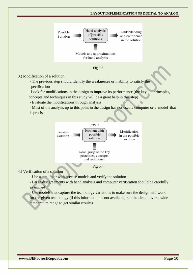
Fig 5.3
3.) Modification of a solution
- The previous step should identify the weaknesses or inability to satisfy the
specifications
- Look for modifications in the design to improve its performance (the key principles,
concepts and techniques in this study will be a great help in this step)
- Evaluate the modifications through analysis
- Most of the analysis up to this point in the design has not used a computer or a model that
is precise
Fig 5.4
4.) Verification of a solution
- Use a simulator with precise models and verify the solution
- Large disagreements with hand analysis and computer verification should be carefully
examined
- Use models that capture the technology variations to make sure the design will work
for the given technology (if this information is not available, run the circuit over a wide
temperature range to get similar results)

LAYOUT IMPLEMENTATION OF DIGITAL TO ANALOG
www.BEProjectReport.com Page 11
5.3 PHYSICAL DESIGN
Physical design is the process of representing the electrical design in a layout consisting of
many distinct geometrical rectangles at various levels. The layout is then used to create the actual,
three-dimensional integrated circuit through a process called fabrication.
Fig 5.5
5.3.1 What is the Purpose of the Layout?
The layout is used to create the masks that enable the fabrication of the chip.
Metal level mask example:
Fig 5.6
5.3.2 Layout Process
1.) The inputs are the W/L values and the schematic (generally from schematic entry used for
simulation).
2.) A tool is used to enter the various geometries. The designer must enter the location, shape, and
level of the particular geometry.
3.) During the layout, the designer must obey a set of rules called design rules. These rules are for the
purpose of ensuring the robustness and reliability of the technology.

LAYOUT IMPLEMENTATION OF DIGITAL TO ANALOG
www.BEProjectReport.com Page 12
4.) Once the layout is complete, then a process called layout versus schematic (LVS) is applied to
determine if the physical layout represents the electrical schematic.
5.) The next step is now that the physical dimensions of the design are known, the parasitics can be
extracted. These parasitics primarily include:
a.) Capacitance from a conductor to ground
b.) Capacitance between conductors
c.) Bulk resistance
6.) The extracted parasitics are entered into the simulated database and the design resimulated to
insure that the parasitics will not cause the design to fail.
5.4.1 Fabrication Process Flow
This topic briefly describes a simplified version of the fabrication of a transistor on the
silicon wafer. The ability to visualize the cross-section of a layout is a basic skill that all layout
designers should master.
Note that each processing step requires that certain areas are defined on chip by appropriate
masks. Consequently, the integrated circuit may be viewed as a set of patterned layers of doped
silicon, polysilicon, metal and insulating silicon dioxide. In general, a layer must be patterned before
the next layer of material is applied on chip. The process used to transfer a pattern to a layer on the
chip is called lithography. Since each layer has its own distinct patterning requirements, the
lithographic sequence must be repeated for every layer, using a different mask.
To illustrate the fabrication steps involved in patterning silicon dioxide through optical
lithography, let us first examine the process flow shown below
Step 1: Well formation stage. Implants n-type impurities into the wafer followed by diffusing the
impurities deep into the substrate to form the N-Wells. For CMOS process, the silicon substrate is
usually p-type.
Fig 5.7
Step 2: Active & isolation stage. Thick oxide is grown outside the active areas. Active areas are
defined as areas where the CMOS transistors are fabricated. Thick oxide is also known as field
oxide. Field oxides isolate the transistors from one another.

LAYOUT IMPLEMENTATION OF DIGITAL TO ANALOG
www.BEProjectReport.com Page 13
Fig 5.8
The first two steps describe a formation of a conventional well. The depth and doping profile of a
conventional well are controlled by the diffusion drive-in at high temperature. A better way to form
the well, known as retrograde well, is usually used in 0.25um 1 and smaller process technologies.
Retrograde well is formed by very high energy implantation. The depth and doping profile of a
retrograde well are controlled by implantation energy and impurity dose. Retrograde well is formed
AFTER the field oxide. Since retrograde well does not require diffusion drive-in, it has smaller
lateral diffusion and a more ideal doping profile.
Step 3: Gate oxide formation stage. A thin gate oxide is grown across the wafer. Gate oxide of only
tens of silicon oxide atoms thick is created during the fabrication process with the current
technology. Gate oxide is the insulator between the transistor‘s gate and its channel. Gate oxide
refers to the ―O‖ in ―MOS‖ which stands for Metal-Oxide-Semiconductor.
Fig 5.9
Step 4: Gate formation stage. Poly (i.e. poly-silicon) is deposited on the wafer. The poly that are
deposited on the gate oxides are the gates of the transistors which are usually known as gate poly.
The gate poly will incline upward when it extends over the field oxide. The gate oxide in the active
area that are not covered by the gate poly will be etched away to form the source and the drain of the
transistor.
Fig 5.10
LAYOUT IMPLEMENTATION OF DIGITAL TO ANALOG
www.BEProjectReport.com Page 14
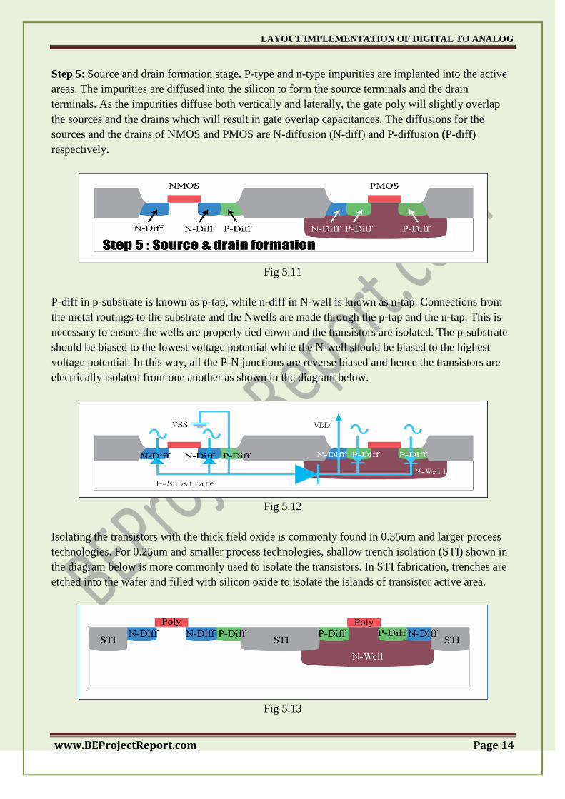
Step 5: Source and drain formation stage. P-type and n-type impurities are implanted into the active
areas. The impurities are diffused into the silicon to form the source terminals and the drain
terminals. As the impurities diffuse both vertically and laterally, the gate poly will slightly overlap
the sources and the drains which will result in gate overlap capacitances. The diffusions for the
sources and the drains of NMOS and PMOS are N-diffusion (N-diff) and P-diffusion (P-diff)
respectively.
Fig 5.11
P-diff in p-substrate is known as p-tap, while n-diff in N-well is known as n-tap. Connections from
the metal routings to the substrate and the Nwells are made through the p-tap and the n-tap. This is
necessary to ensure the wells are properly tied down and the transistors are isolated. The p-substrate
should be biased to the lowest voltage potential while the N-well should be biased to the highest
voltage potential. In this way, all the P-N junctions are reverse biased and hence the transistors are
electrically isolated from one another as shown in the diagram below.
Fig 5.12
Isolating the transistors with the thick field oxide is commonly found in 0.35um and larger process
technologies. For 0.25um and smaller process technologies, shallow trench isolation (STI) shown in
the diagram below is more commonly used to isolate the transistors. In STI fabrication, trenches are
etched into the wafer and filled with silicon oxide to isolate the islands of transistor active area.
Fig 5.13

LAYOUT IMPLEMENTATION OF DIGITAL TO ANALOG
www.BEProjectReport.com Page 15
5.5 PACKAGING
Packaging of the integrated circuit is an important part of the physical design process.
The function of packaging is:
1.) Protect the integrated circuit
2.) Power the integrated circuit
3.) Cool the integrated circuit
4.) Provide the electrical and mechanical connection between the integrated circuit and the
outside world.
Packaging steps:
Fig 5.14

LAYOUT IMPLEMENTATION OF DIGITAL TO ANALOG
www.BEProjectReport.com Page 16
CHAPTER 6
RELIABILITY ISSUES AND YIELD
1. Latch up
2. Electro migration
3. ESD
6.1 LATCH UP:
The structure of a bulk CMOS process introduces a problem known as latch-up in which the
circuits fail to operate and the chip draws excessive power supply current.
A problem which is inherent in the p-well and n-well process is due to the relevantly large
number of junctions which are formed in these structures and, the consequent presence of parasitic
transistor and diodes, Latchup is a condition in which the parasitic components give rise to the
establishment of low resistance conducting paths between VDD and VSS with disastrous results.
Careful control during fabrication is necessary to avoid this problem.
Consider the n-well structure of Fig 6.1. The n-p-n-p structure is formed by the source of the
NMOS, the p-substrate, the n-well and the sources of the PMOS. An equivalent circuit is shown in
Fig 6.2. when one of the two bipolar transistors gets forward-biased (e.g., due to current flowing
through the well or substrate), it feeds the base of the other transistor. This positive feedback
increases the current until the circuit fails or burns out.
Fig 6.1

LAYOUT IMPLEMENTATION OF DIGITAL TO ANALOG
www.BEProjectReport.com Page 17
Fig 6.2
The remedies for the latchup problem include:
i. An increase in substrate doping levels with a consequent drop in the value of Rpsub.
ii. Reducing Rnwell by control of fabrication parameters and ensuring a low contact resistance to
VDD
iii. By introducing guard rings.
6.2.1 Electro Migration (EM):
Electro migration is the diffusion of metal atoms along the conductor in the direction of electron flow.
This directional diffusion process occurs because the momentum transfer between the electrons and
the metal atoms increases the probability that an aluminum atom will move in the direction of the
electron flow. Since the mass of the electron is very much smaller than aluminum atoms the transfer
of momentum is only enough to have a statistical effect upon the diffusion of aluminum. This
diffusion process will preferentially fill metal ion vacancies found in crystal defects, leaving a
vacancy in the location from which the metal atom came.
The flow of metal ions in the direction of electron flow in itself does not cause damage to the
aluminum wires. Damage only occurs when there is a metal ion flux divergence that causes metal
ions to be taken from one part of a wire and deposit them in some other location without replenishing
the metal ions from a reservoir. The flux divergence causes vacancies to coalesce in one location to
produce a void. This void volume grows until there is no aluminum in a short length of the wire;
causing current flow is interrupted leading to circuit failure.
6.2.2 Electro Migration – Failure Modes:
Electro migration occurs when some of the momentum of a moving electron is transferred to
a nearby activated ion. This causes the ion to move from its original position.
a) Over time this force knocks a significant number of atoms far from their original positions. A
break or gap can develop in the conducting material, preventing the flow of electricity. In narrow
interconnect conductors, such as those linking transistors and other components in integrated circuits,
this is known as a void or internal failure open circuit. (Fig 6.3.a)

LAYOUT IMPLEMENTATION OF DIGITAL TO ANALOG
www.BEProjectReport.com Page 18
b) Electro migration can also cause the atoms of a conductor to pile up and drift toward other nearby
conductors, creating an unintended electrical connection known as a hillock failure or whisker
failure (short circuit). (Fig 6.3.b)
Both of these situations can lead to a malfunction of the circuit.
Fig 6.3, a, b
6.3 ELECTRO STATIC DISCHARGES (ESD):
Electrostatic discharge is defined as the transfer of charge between bodies at different electric
potentials. The amount of charge created by contact charging is affected by the area of contact, the
speed of separation, relative humidity, and other factors.
6.3.1 Damage from ESD’s can
Cause complete device failure by parametric shifts, or
Device weakness by locally heating, melting or otherwise damaging oxides, junctions
or device components
6.3.2 Remedies
Special circuitry with ESD protection diodes, guard rings etc.
6.4 YIELD CONSIDERATIONS:
6.4.1 Yield:
High-density chip designs consist of a few tens of millions of MOSFETs. This has become so
common place that the technical achievement of silicon processing is generally overlooked. Consider
the implications of having a ―good die‖. This means that, so far as the testing process has shown,
every circuit in the die operates as it should. In other words, every important feature of every
transistor and the interconnect wiring has the correct behavior and, therefore, the correct structure. In
the real world of semiconductor manufacturing, we are continually faced with the fact that only a
percentage of the die is functional. This is expressed by the yield Y of a process such that
Obviously, a high yield is required to have a profitable design.
LAYOUT IMPLEMENTATION OF DIGITAL TO ANALOG
www.BEProjectReport.com Page 19
CHAPTER 7
INSTRUCTION TO 0.13UM DESIGN & IMPORTANCE OF THE
RULES
7.1 DESIGN RULES & SIGNIFICANCE:
Design Rules are a series of parameters provided by semiconductor manufacturers that enable
the designer to verify the correctness of a mask set. Design rules are specific to a particular
semiconductor manufacturing process. A design rule set specifies certain geometric and connectivity
restrictions to ensure sufficient margins to account for variability in semiconductor manufacturing
processes, so as to ensure that most of the parts work correctly.
7.1.1 In General Design Rules:
Design rules govern the layout of individual components: transistors, wires, contacts, vias
How small can the gates be, and how small can the wires be made
Conflicting Demands:
Component packing: more functionality, higher speed
Chip yield: smaller sizes can reduce yield (fraction of good chips)
Conservative vs aggressive design rule
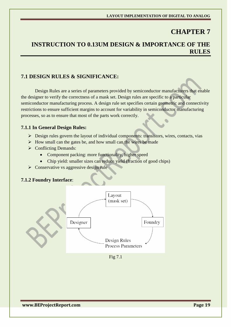
7.1.2 Foundry Interface:
Fig 7.1

LAYOUT IMPLEMENTATION OF DIGITAL TO ANALOG
www.BEProjectReport.com Page 20
7.2 DESIGN RULE VIOLATION:
Violating a design rule might result in a non-functional circuit or low yield.
Fig 7.2
7.3 TYPES OF DESIGN RULES:
Scalable Design Rules: Lambda parameter
Based on scalable ―coarse grid‖ - L (lambda).
Idea: reduce L value for each new process, but keep rules the same.
Key advantage: portable layout.
Key disadvantage: not everything scales the same.
Not used in ―real life‖.
Absolute Dimensions (micron rules)
Based on absolute distances (e.g. 0.75µm).
Layouts not portable.
7.4:0.13u Design rules for TSMC (Taiwan Semiconductor Manufacturing Company) Fab
House:
DESIGN RULES OF .13µM TSMC
Cell Height 3.690
Rail Height 0.50
POLY
1 Width 0.13
2 Minimum Width(Interconnect) 0.13
3 Minimum Space 0.18
4 Minimum Space On OD 0.18
5 Minimum Field Poly Space To OD 0.07
6 Minimum OD Extension On Poly 0.23
7 Minimum PO Extension On OD 0.18
metal1 metal1
After Fabrication
Spacing violation
After Fabrication
Width violation

LAYOUT IMPLEMENTATION OF DIGITAL TO ANALOG
www.BEProjectReport.com Page 21
8 Minimum Poly Area 0.09
9 Minimum Enclosed Area 0.15
METAL 1
1 Minimum Width 0.16
2 Minimum Space 0.18
3 Minimum Enclosure Of Contact 0.00
4 Minimum Area 0.122
5 Minimum Enclosure Of Contact (End Of Line) 0.05
6 Minimum Enclosed Area 0.2
CONTACT
1 Size 0.16X0.16
2 Minimum Space 0.18
3 Minimum Enclosed By Active 0.07
4 Minimum Enclosed By Poly 0.07
5 Minimum Gate Spacing ( Inside OD) 0.11
6 Contact Inside Poly, Minimum Space To OD 0.14
OD
1 Minimum Width 0.15
2 Minimum Space 0.21
3 Minimum N+ Active Space To Nwell 0.31
4 Minimum P+ Active Enclose By Nwell 0.31
5 Minimum Area 0.122
PP
1 Minimum Width 0.31
2 Minimum Space 0.31
3 Minimum Space To N+ Active 0.18
4 Minimum Area 0.25
5 Minimum Extension On Pactive 0.18
NP
1 Minimum Width 0.31
2 Minimum Space 0.31
3 Minimum Space To P+ Active 0.18
4 Minimum Area 0.25
5 Minimum Extension On Nactive 0.18

LAYOUT IMPLEMENTATION OF DIGITAL TO ANALOG
www.BEProjectReport.com Page 22
CHAPTER 8
STICK DIAGRAMS & FOLDING CONCEPT
8.1 STICK DIAGRAMS:
Stick diagrams provide an easy approach to performing simple CMOS circuit layouts.
Planning a physical design using stick diagrams before going to CAD tool can save a lot of time and
energy.
They are useful for planning the layout and routing of integrated circuits. In a stick diagram,
every line of a conducting material layer is represented by a line of a distinct color. For below given
examples we will use basic color coding:
Fig 8.1
Other layers will be introduced later.
The width of a line is not important, as stick diagrams give only wiring and routing
information.
A stick diagram is thus a schematic representation of a circuit at physical design level. With a
practice we will be able to read a stick diagram and translate it into a conventional circuit schematic.
Fig 8.2
In terms of stick diagrams, we say that an nFET is formed whenever Red (Poly) crosses over Green
(Active).
Fig 8.3
LAYOUT IMPLEMENTATION OF DIGITAL TO ANALOG
www.BEProjectReport.com Page 23
This is consistent with top view of a transistor.
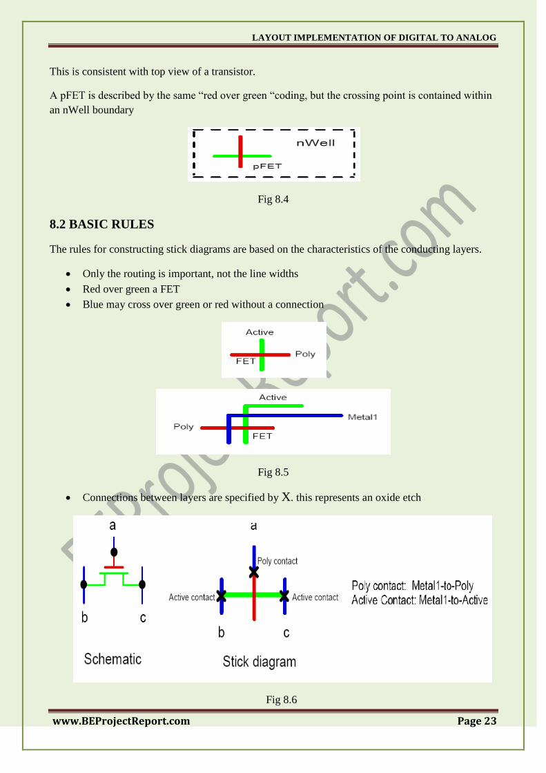
A pFET is described by the same ―red over green ―coding, but the crossing point is contained within
an nWell boundary
Fig 8.4
8.2 BASIC RULES
The rules for constructing stick diagrams are based on the characteristics of the conducting layers.
Only the routing is important, not the line widths
Red over green a FET
Blue may cross over green or red without a connection
Fig 8.5
Connections between layers are specified by X. this represents an oxide etch
Fig 8.6

LAYOUT IMPLEMENTATION OF DIGITAL TO ANALOG
www.BEProjectReport.com Page 24
Metal lines on different layers can cross one another. Contacting two metal lines require a via
Fig 8.7
8.3 EXAMPLES
Fig 8.8
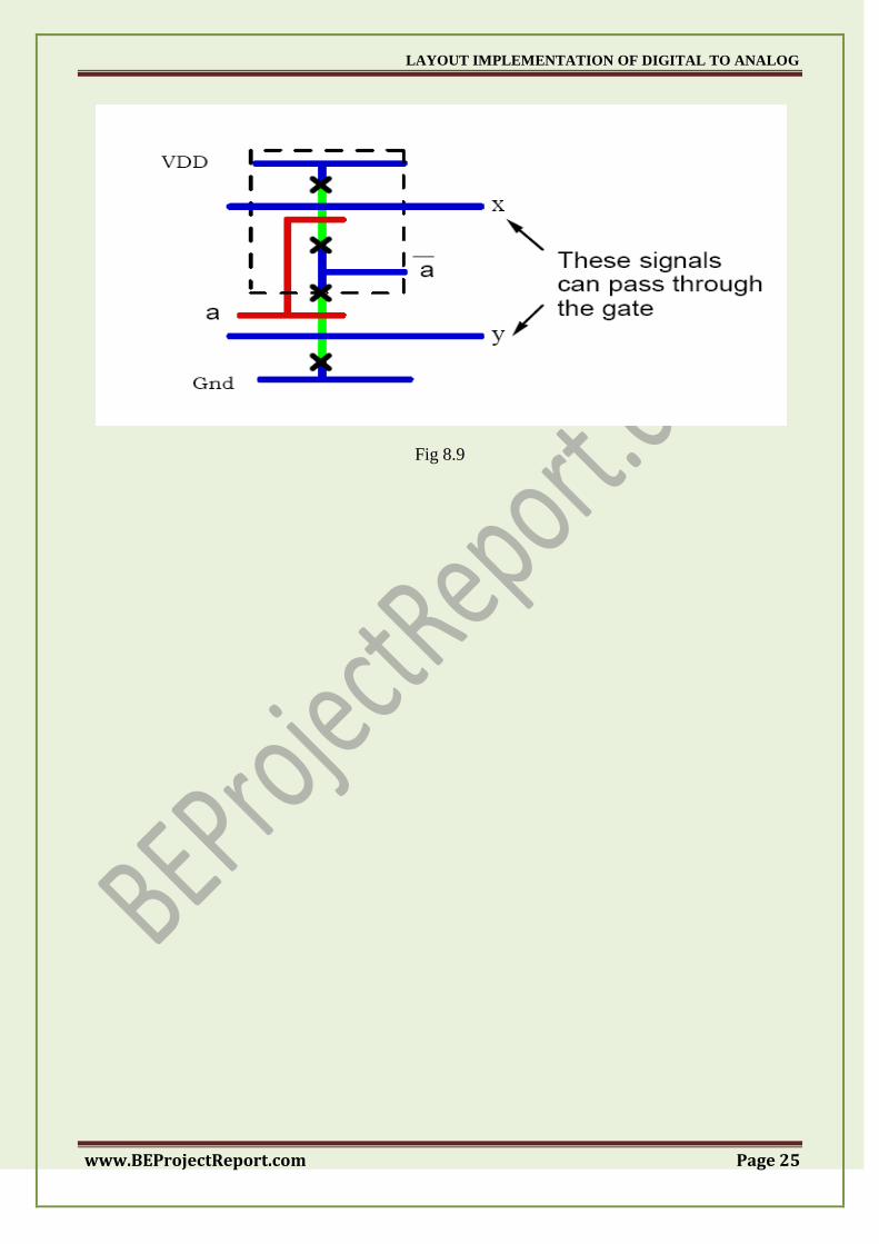
Stick diagrams are often used to solve routing problems.
LAYOUT IMPLEMENTATION OF DIGITAL TO ANALOG
www.BEProjectReport.com Page 25
Fig 8.9
LAYOUT IMPLEMENTATION OF DIGITAL TO ANALOG
www.BEProjectReport.com Page 26
CHAPTER 9
LAYOUTS OF STD CELLS (DIGITAL) WITH NET LIST
9.1 STANDARD CELL DESCRIPTIONS
9.1.1 Inverter:
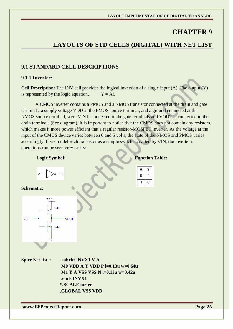
Cell Description: The INV cell provides the logical inversion of a single input (A). The output (Y)
is represented by the logic equation. Y = A!.
A CMOS inverter contains a PMOS and a NMOS transistor connected at the drain and gate
terminals, a supply voltage VDD at the PMOS source terminal, and a ground connected at the
NMOS source terminal, were VIN is connected to the gate terminals and VOUT is connected to the
drain terminals.(See diagram). It is important to notice that the CMOS does not contain any resistors,
which makes it more power efficient that a regular resistor-MOSFET inverter. As the voltage at the
input of the CMOS device varies between 0 and 5 volts, the state of the NMOS and PMOS varies
accordingly. If we model each transistor as a simple switch activated by VIN, the inverter‘s
operations can be seen very easily:
Logic Symbol: Function Table:
Schematic:
Spice Net list : .subckt INVX1 Y A
M0 VDD A Y VDD P l=0.13u w=0.64u
M1 Y A VSS VSS N l=0.13u w=0.42u
.ends INVX1
*.SCALE meter
.GLOBAL VSS VDD
LAYOUT IMPLEMENTATION OF DIGITAL TO ANALOG
www.BEProjectReport.com Page 27
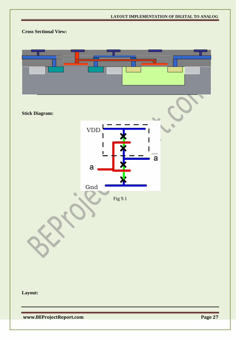
Cross Sectional View:
Stick Diagram:
Fig 9.1
Layout:
LAYOUT IMPLEMENTATION OF DIGITAL TO ANALOG
www.BEProjectReport.com Page 28
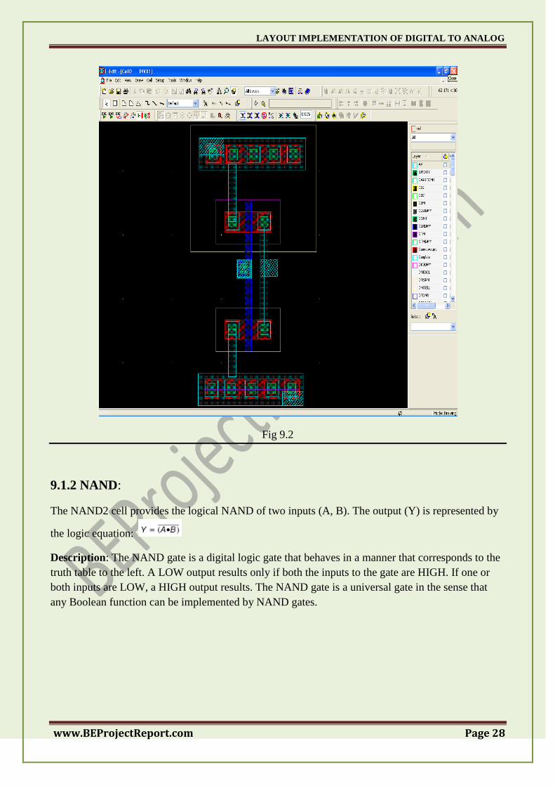
Fig 9.2
9.1.2 NAND:
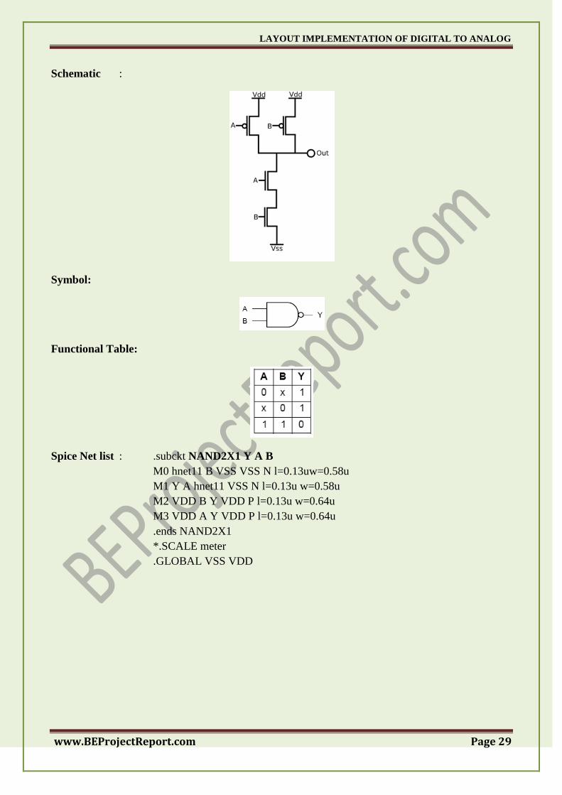
The NAND2 cell provides the logical NAND of two inputs (A, B). The output (Y) is represented by
the logic equation:
Description: The NAND gate is a digital logic gate that behaves in a manner that corresponds to the
truth table to the left. A LOW output results only if both the inputs to the gate are HIGH. If one or
both inputs are LOW, a HIGH output results. The NAND gate is a universal gate in the sense that
any Boolean function can be implemented by NAND gates.
LAYOUT IMPLEMENTATION OF DIGITAL TO ANALOG
www.BEProjectReport.com Page 29
Schematic :
Symbol:
Functional Table:
Spice Net list : .subckt NAND2X1 Y A B
M0 hnet11 B VSS VSS N l=0.13uw=0.58u
M1 Y A hnet11 VSS N l=0.13u w=0.58u
M2 VDD B Y VDD P l=0.13u w=0.64u
M3 VDD A Y VDD P l=0.13u w=0.64u
.ends NAND2X1
*.SCALE meter
.GLOBAL VSS VDD

LAYOUT IMPLEMENTATION OF DIGITAL TO ANALOG
www.BEProjectReport.com Page 30
Stick diagram:
Fig 9.3
Layout:
Fig 9.4
LAYOUT IMPLEMENTATION OF DIGITAL TO ANALOG
www.BEProjectReport.com Page 31
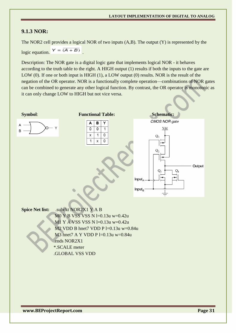
9.1.3 NOR:
The NOR2 cell provides a logical NOR of two inputs (A,B). The output (Y) is represented by the
logic equation. .
Description: The NOR gate is a digital logic gate that implements logical NOR - it behaves
according to the truth table to the right. A HIGH output (1) results if both the inputs to the gate are
LOW (0). If one or both input is HIGH (1), a LOW output (0) results. NOR is the result of the
negation of the OR operator. NOR is a functionally complete operation—combinations of NOR gates
can be combined to generate any other logical function. By contrast, the OR operator is monotonic as
it can only change LOW to HIGH but not vice versa.
Symbol: Functional Table: Schematic:
Spice Net list: .subckt NOR2X1 Y A B
M0 Y B VSS VSS N l=0.13u w=0.42u
M1 Y A VSS VSS N l=0.13u w=0.42u
M2 VDD B hnet7 VDD P l=0.13u w=0.84u
M3 hnet7 A Y VDD P l=0.13u w=0.84u
.ends NOR2X1
*.SCALE meter
.GLOBAL VSS VDD
LAYOUT IMPLEMENTATION OF DIGITAL TO ANALOG
www.BEProjectReport.com Page 32
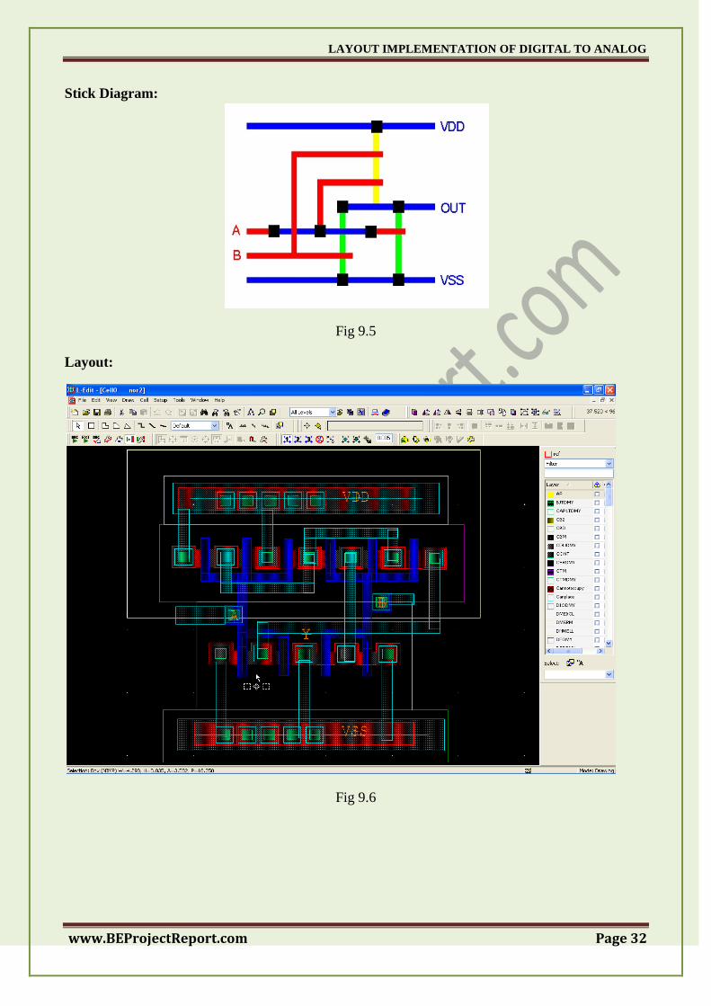
Stick Diagram:
Fig 9.5
Layout:
Fig 9.6

LAYOUT IMPLEMENTATION OF DIGITAL TO ANALOG
www.BEProjectReport.com Page 33
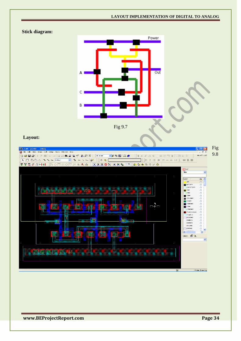
9.1.4 OAI21X1:
The AOI21cell provides the logical inverted OR of one AND group and an additional input. The
output (Y) is represented by the logic equation:
Logic Symbol:
A0
A1
Y
B0
Functional Table:
Schematic:
Spice Net list:
.subckt OAI21X1 Y A0 A1 B0
M0 VDD A1 hnet11 VDD P l=0.13u w=0.84u
M1 hnet11 A0 Y VDD P l=0.13u w=0.84u
M2 Y B0 net25 VSS N l=0.13u w=0.58u
M3 net25 A1 VSS VSS N l=0.13u w=0.58u
M4 net25 A0 VSS VSS N l=0.13u w=0.58u
M5 Y B0 VDD VDD P l=0.13u w=0.64u
.ends OAI21X1
*.SCALE meter
.GLOBAL VSS VDD
A0, A1 & B0 are inputs & Y is output
LAYOUT IMPLEMENTATION OF DIGITAL TO ANALOG
www.BEProjectReport.com Page 34
Stick diagram:
Fig 9.7
Layout:
Fig
9.8

LAYOUT IMPLEMENTATION OF DIGITAL TO ANALOG
www.BEProjectReport.com Page 35
CHAPTER 10
LAYOUT TECHNIQUE IN ANALOG
10.1 ANALOG LAYOUT:
Device Matching
- Why do I care?
- Matching ‗theory‘
- Basic approach for transistors, capacitors, resistors
Noise and Decoupling
- Capacitive coupling
- Substrate noise
- Thermal noise
- Shielding
10.2 ANALOG DESIGNERS THINK A LOT ABOUT MATCHING:
• Basic operation of some circuits depends directly on matchingeg. pipelined A/D converters
• Common-mode rejection limited by matching
Common-mode to differential-mode conversion is proportional to mismatch
• Supply noise rejection limited by mismatch in fully-differential circuits
In fully-differential circuits supply noise appears like a common-mode signal applied to the supply
• Amplifier offsets greatly degrade the performance of band gap references
Digital designers also care about matching of transistors and routing because of skew and in
memories.
If you follow some simple rules, you can avoid gross matching problems. If you‘re trying to ratio
two transistors
• Use the same W and L and vary M (takes out ΔW and ΔL effects)
• Use M‘s that are even, preferably factors of 4 (transistors are not truly symmetrical!)
• Use common-centroid, or nearly common-centroid, layout (takes out oxide and doping gradients)

LAYOUT IMPLEMENTATION OF DIGITAL TO ANALOG
www.BEProjectReport.com Page 36
• Use dummy transistors at the ends of the row (takes out poly etch loading and mask misalignment
effects)
• Make clean and well balanced routing
• Use a suitable area and overdrive
• Use plenty of substrate and well taps
• Route currents a long way, not voltages - IR drops can cause big Mismatches
10.3 SYSTEMATIC MISMATCH
Systematic mismatch refers to a spatial gradient in component values. It is very undesirable: it can be
very large and swamp out random mismatch, it can cause various circuit problems such as harmonic
distortion in A/D converters, while random mismatch is usually somewhat more benign in its impact
on higher level specs.
Systematic mismatch can be caused by processing gradients and inadequate layout. Follow the rules
of matching.
Imbalanced loads can look like a systematic mismatch: eg. The strobe signal in an edge triggered
regenerative latch can easily imbalance the circuit by 100mV! This is hard to distinguish from a
static offset in the test lab although it is a dynamic effect.
A good test of the symmetry of routing is a power supply rejection simulation on the back annotated
net list.
10.4 MATCHING CAPACITORS AND RESISTORS
To match caps and resistors, use unit cells and dummy edge devices
Fig 11.1

LAYOUT IMPLEMENTATION OF DIGITAL TO ANALOG
www.BEProjectReport.com Page 37
10.5 MATCHING TECHNIQUES
Goals of Good Analog Layout
Minimum parasitics
Low crosstalk
Less Area
Minimum substrate Noise
Good Device matching
10.6 SYMMETRY:
Fig 11.3
Consider matching two transistors: A and B (DASBD)
- Orientation mismatch develops due to diagonal shift in S/D implantation
- Tilted implant cause S/D to differ
- If devices are arranged in (DASBD), drain of left differs from drain of right
- A Small difference in Tran conductance
- mismatch worse at high voltage, as titled implant has string impact on hot carrier effect
- This problem is cancelled if they have equal chirality

LAYOUT IMPLEMENTATION OF DIGITAL TO ANALOG
www.BEProjectReport.com Page 38
CHAPTER 11
PHYSICAL VERIFICATION (DRC & LVS FLOW) &SAMPLE RUN
SETS FOR DRC & LVS
11.1 PHYSICAL VERIFICATION (DRC/LVS):
Physical verification is a process whereby an IC layout design is checked via EDA software
tools to see if it meets certain criteria. Verification involves DRC (Design rule check), LVS (Layout
versus schematic), ERC (Electrical Rule Check), and Antenna Checks.
Physical Verification Flow:
Fig 12.1
11.2 DESIGN RULE CHECK (DRC)
11.2.1 Design Rule Checking Software
The main objective of design rule checking (DRC) is to achieve a high overall yield and reliability
for the design. If design rules are violated the design may not be functional. To meet this goal of
improving die yields, DRC has evolved from simple measurement and Boolean checks, to more
involved rules that modify existing features, insert new features, and check the entire design for
process limitations such as layer density. A completed layout consists not only of the geometric
representation of the design, but also data that provides support for the manufacture of the design.
While design rule checks do not validate that the design will operate correctly, they are constructed
to verify that the structure meets the process constraints for a given design type and process
technology.
DRC software usually takes as input a layout in the GDSII standard format and a list of rules
specific to the semiconductor process chosen for fabrication. From these it produces a report of
design rule violations that the designer may or may not choose to correct. Carefully "stretching" or
LAYOUT IMPLEMENTATION OF DIGITAL TO ANALOG
www.BEProjectReport.com Page 39
waiving certain design rules is often used to increase performance and component density at the
expense of yield.
Some example of DRC‘s in IC design includes:
Active to active spacing
Well to well spacing
Minimum channel length of the transistor
Minimum metal width
Metal to metal spacing
Metal fill density (for processes using CMP)
ESD and I/O rules
11.2.2 Design Rule Sets
It is not usually necessary to create design rules sets from scratch. If you have a previous
design file that uses a set of rules similar to those you want to employ in your current design, you can
modify the rule set from the previous design.
In general, you must perform the following three steps to create or edit a design rule set:
1. Determine which rules must be specified. Fabrication services or foundries are typically able to
provide design rule sets.
2. Determine which generated layers, if any, will be needed to implement each rule in the set.
3. Enter the rules in the Setup Design Rules.
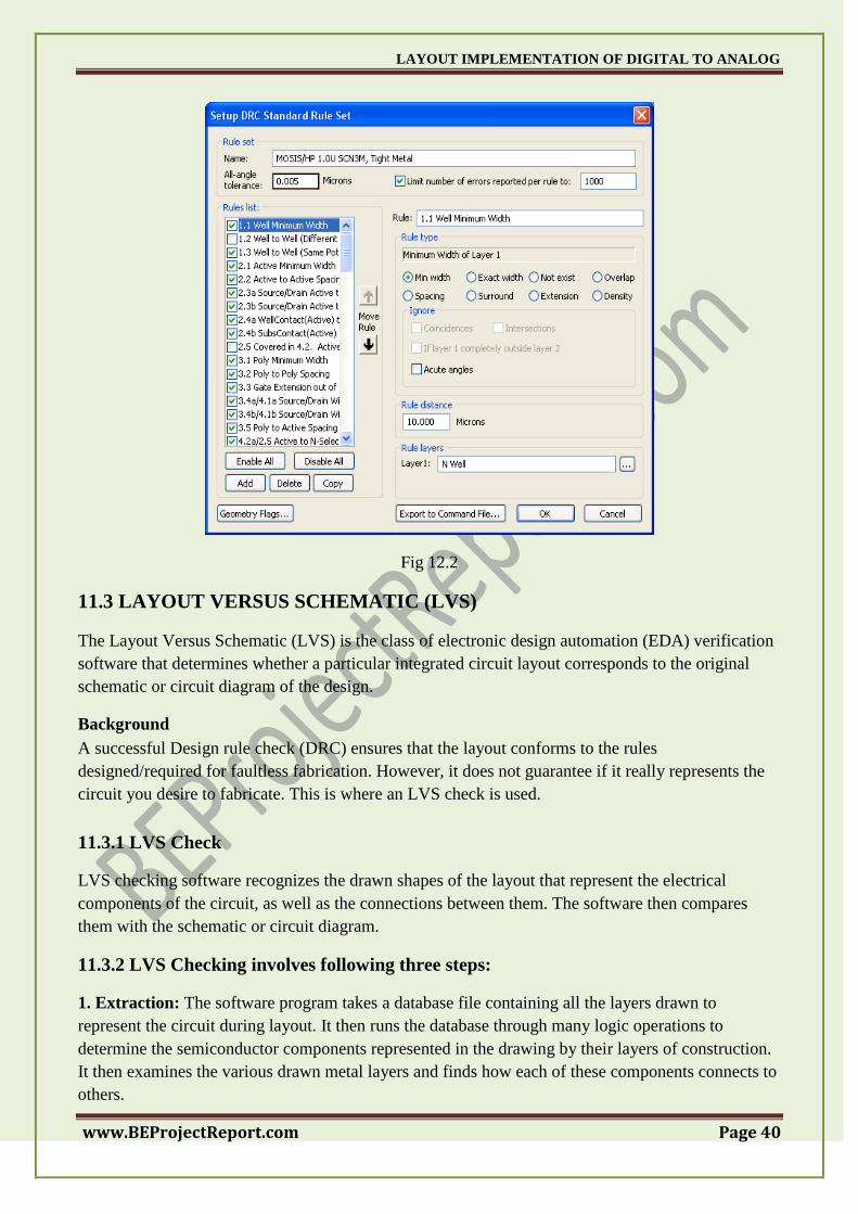
11.2.3 Specifying DRC Standard Design Rules
Select Tools > DRC Setup from the menu, highlight DRC Standard Rule Set in the rule set list,
then press the Edit button ( ) to open the Setup DRC Standard Rule Set dialog, which allows you to
modify the DRC standard design rules.
LAYOUT IMPLEMENTATION OF DIGITAL TO ANALOG
www.BEProjectReport.com Page 40
Fig 12.2
11.3 LAYOUT VERSUS SCHEMATIC (LVS)
The Layout Versus Schematic (LVS) is the class of electronic design automation (EDA) verification
software that determines whether a particular integrated circuit layout corresponds to the original
schematic or circuit diagram of the design.
Background
A successful Design rule check (DRC) ensures that the layout conforms to the rules
designed/required for faultless fabrication. However, it does not guarantee if it really represents the
circuit you desire to fabricate. This is where an LVS check is used.
11.3.1 LVS Check
LVS checking software recognizes the drawn shapes of the layout that represent the electrical
components of the circuit, as well as the connections between them. The software then compares
them with the schematic or circuit diagram.
11.3.2 LVS Checking involves following three steps:
1. Extraction: The software program takes a database file containing all the layers drawn to
represent the circuit during layout. It then runs the database through many logic operations to
determine the semiconductor components represented in the drawing by their layers of construction.
It then examines the various drawn metal layers and finds how each of these components connects to
others.

LAYOUT IMPLEMENTATION OF DIGITAL TO ANALOG
www.BEProjectReport.com Page 41
2. Reduction: During reduction the software combines the extracted components into series and
parallel combinations if possible and generates a netlist representation of the layout database.
3. Comparison: The extracted layout netlist is then compared to the netlist taken from the circuit
schematic. If the two netlists match, then the circuit passes the LVS check. At this point it is said to
be "LVS clean."
Fig 12.3
11.4 EXAMPLES OF LVS ERRORS
In most cases the layout will not pass LVS the first time requiring the layout engineer to examine the
LVS software's reports and make changes to the layout. Typical errors encountered during LVS
include:
1. Shorts: Two or more wires that should not be connected together have been and must be separated.
2. Opens: Wires or components that should be connected are left dangling or only partially
connected. These must be connected properly to fix this.
3. Component Mismatches: Components of an incorrect type have been used (e.g. a low Vt MOS
device instead of a standard Vt MOS device)
4. Missing Components: An expected component has been left out of the layout.
5. Property Errors: A component is the wrong size compared to the schematic.
In some cases of property errors, where it is not critical to performance, the designer may modify the
schematic to match the layout.

LAYOUT IMPLEMENTATION OF DIGITAL TO ANALOG
www.BEProjectReport.com Page 42
11.4.1 LVS: Extract Errors – Short
Same net named with different pin names
Example:
Fig 12.4
LVS: Extract Errors – Short (Contd.)
Two different nets shorting together.
Example - A and B are shorted being on the same net ―net1‖.
Fixing:
Two nets: n1 connected to Pin: A, n2 connected to Pin: B Accidentally got shorted, during routing.
Left is a problem, right is the fix.
Fig 12.5
A
A
B
A
LAYOUT IMPLEMENTATION OF DIGITAL TO ANALOG
www.BEProjectReport.com Page 43
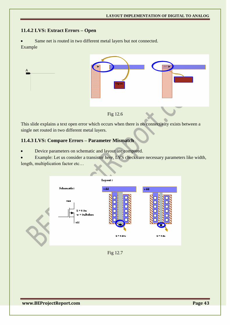
11.4.2 LVS: Extract Errors – Open
Same net is routed in two different metal layers but not connected.
Example
Fig 12.6
This slide explains a text open error which occurs when there is no connectivity exists between a
single net routed in two different metal layers.
11.4.3 LVS: Compare Errors – Parameter Mismatch
Device parameters on schematic and layout are compared.
Example: Let us consider a transistor here, LVS checks are necessary parameters like width,
length, multiplication factor etc…
Fig 12.7
A

LAYOUT IMPLEMENTATION OF DIGITAL TO ANALOG
www.BEProjectReport.com Page 44
11.4.4 LVS: Compare Errors – Device/Net Mismatch
Fig 12.8
Here we are discussing about a Device mismatch and net mismatch error. In the schematic net 1 is
connected to pin A of nand2 and net 2 is connected to pin B of nand2, in the incorrect layout net 2 is
connected to pin A and net 1 is connected to pin B. which is fixed in on the right hand side layout.
This leads to device mismatch and net mismatch errors.
11.4.5 LVS: Compare Errors – Pin Errors
Fig 12.9
This slide explains an LVS pin error which occurs when pins on schematic and layout are not
matching. In the figure nand2 schematic has two pins namely a and b but layout of nand2 has only
pin a and pin b is missing which leads to a pin error.
LVS: Compare Errors – Malformed Devices

LAYOUT IMPLEMENTATION OF DIGITAL TO ANALOG
www.BEProjectReport.com Page 45
Fig 12.10
Here we are explaining malformed devices which are created accidentally when a poly crosses
diffusion. These devices are unintentional and should be removed from the design.
11.5 EXTRACT DEFINITION FILE FORMAT
The extract definition file contains a list of comments, connection statements, and device statements.
L-Edit is shipped with a directory containing a set of extract definition files that correspond to
various technology processes. You can modify these files as necessary to define additional
connections and devices for extraction.
11.5.1 Extract definition files must conform to the following restrictions:
Layer names are case-sensitive, and must match the case of layer names defined in the TDB
file.
The rest of the definition file is case-insensitive; upper and lower cases can be used
interchangeably.
Layer names cannot contain commas or semicolons and they cannot be longer than 40
characters.
Layer names cannot have leading or trailing spaces.
Pin names cannot contain commas, semicolons, or spaces, and they cannot be named
MODEL.
Model names cannot contain commas, semicolons, spaces, or closing parentheses.
for compatibility with existing extract definition files, the WIDTH keyword is ignored for all
devises except a GAASFET/MESFET.
IGNORE_SHORTS indicates that if the device has all of its pins connected to the same
node then it will be considered shorted and the device will be written to the extract net list file
as a comment.

LAYOUT IMPLEMENTATION OF DIGITAL TO ANALOG
www.BEProjectReport.com Page 46
CHAPTER 12
DAC
12.1 BASIC BLOCK DIAGRAM DIGITAL-TO-ANALOG CONVERTER:
Digital-to-analog converter chips transform information from digital to analog form. They convert
signals that have two defined states, on and off, into signals that have a theoretically infinite number
of states
Fig 13.1
8-bit R-2R Ladder Digital To Analog Converter (DAC) with Equal Currents Design and Layout
The project is an 8-bit digital-to-analog converter that utilizes a resister ladder network to
divide current with equal current sources, and an operational amplifier to sum these currents and
convert them into an output voltage. The use of an R-2R ladder architecture is very useful for binary-
weighted currents. However, the R-2R based converter is easy to implement and the resistance ratio
is independent of the number of bits the precision of the resistor is significant. Because the resistance
of the R-2R architecture must be so closely matched (as close as 0.01% for the LSB on an 8-bit
DAC) and the current ratio through the switches is still large the implementation of current sources is
needed. With equal current flow through all the switches the architecture will be slower but more
stable.
12.2 DAC APPLICATIONS
i) Modems convert digital computer data that consists of ones and zeroes into audio
frequency (AF) tones that can be transmitted over telephone lines.
ii) Most modern audio signals are stored in digital form (for example MP3s and CDs) and
in order to be heard through speakers they must be converted into an analog signal. DACs are
therefore found in CD Players, Digital Music Players, and PC Sound Cards.

LAYOUT IMPLEMENTATION OF DIGITAL TO ANALOG
www.BEProjectReport.com Page 47
iii) Specialist stand-alone DACs can also be found in high-end hi-fi systems. These normally
take the digital output of a CD Player (or dedicated transport) and convert the signal into a line-
level output that can then be fed into a pre- Amplifier stage.
iv) Similar digital-to-analog converters can be found in Digital speakers such as USB
speakers, and in Sound Cards.
v) Video signals from a digital source, such as a computer, must be converted to analog
form if they are to be displayed on an analog monitor.
vi) A video DAC is, however, incorporated in any Digital Video Player with analog outputs.
The DAC is usually integrated with some memory(RAM), which contains conversion tables for
gamma correction, contrast and brightness, to make a device called a RAMDAC.
12.3 R-2R LADDER DAC CIRCUIT DIAGRAM:
Objective
The objective of this project is to design an 8-bit R-2R digital-to-analog converter with current
sources in 130nm technology, TSMC and Checking for design rules check (DRC), and Layout vs.
Schematic (LVS).
Design
The basic principle of this type of R-2R DAC is to split the reference currents equally through the
switches. The current sources that were used were N-type transistors with a size of W/L = 5/1.5. The
current sources used a bias generator that produced 1.68V to allow ~80uA of current. The current
sources were necessary for the R-2R DAC to work properly due to the switches and the matching of
the resistors. The high poly 2 resistance (R) was equal to 4kW. The switches used a pass transistor
configuration and had a resistance value of approximately 500W with the size of W/Ln = 25/0.6 and
W/Lp = 50/0.6.
LAYOUT IMPLEMENTATION OF DIGITAL TO ANALOG
www.BEProjectReport.com Page 48
12.3.1 DAC Modules:
1. Inverter – to get compliment binary output
2. Pass Transistor Switch – it is for Bit selection based on its binary weight
3. Current Sources - to produce equal current flow through all the switches
4. Current Source Bias Generator - for current sources (without a resistor)
5. Opamp without Bias Generator - The operational amplifier used in the DAC has 3
stages (Differential – input stage, Common – source stage and an Output buffer).
6. Bias Generator - for the operational amplifier
7. R-2R D/A Convert - R/2R ladder networks provide a simple means to convert digital
information to an analog output

LAYOUT IMPLEMENTATION OF DIGITAL TO ANALOG
www.BEProjectReport.com Page 49
12.3.2 Schematic Diagram of DAC
Fig 13.3
LAYOUT IMPLEMENTATION OF DIGITAL TO ANALOG
www.BEProjectReport.com Page 50
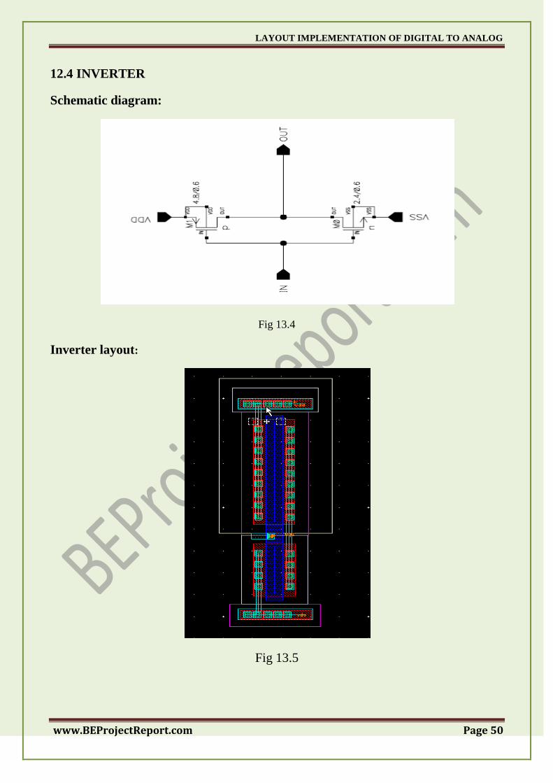
12.4 INVERTER
Schematic diagram:
Fig 13.4
Inverter layout:
Fig 13.5
LAYOUT IMPLEMENTATION OF DIGITAL TO ANALOG
www.BEProjectReport.com Page 51
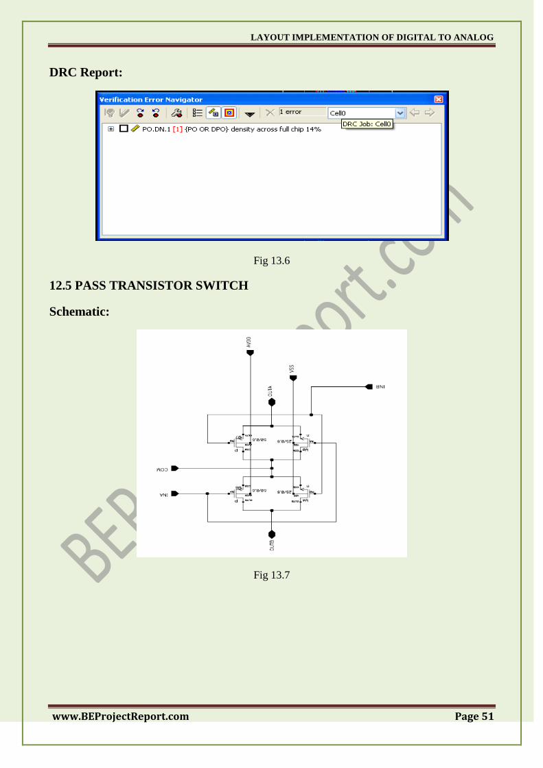
DRC Report:
Fig 13.6
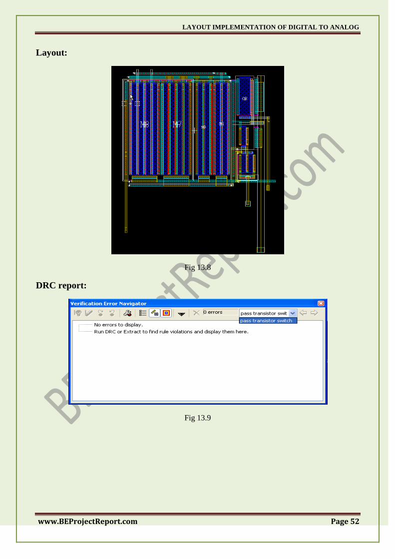
12.5 PASS TRANSISTOR SWITCH
Schematic:
Fig 13.7
LAYOUT IMPLEMENTATION OF DIGITAL TO ANALOG
www.BEProjectReport.com Page 52
Layout:
Fig 13.8
DRC report:
Fig 13.9

LAYOUT IMPLEMENTATION OF DIGITAL TO ANALOG
www.BEProjectReport.com Page 53
12.6 CURRENT SOURCE BIAS GENERATOR
Schematic:
Fig 13.10
Layout:
Fig 13.11
DRC report:

LAYOUT IMPLEMENTATION OF DIGITAL TO ANALOG
www.BEProjectReport.com Page 54
Fig 13.12
12.7 OPAMP WITHOUT BIAS GENERATOR
Schematic:
Fig 13.13
Layout:
Block1
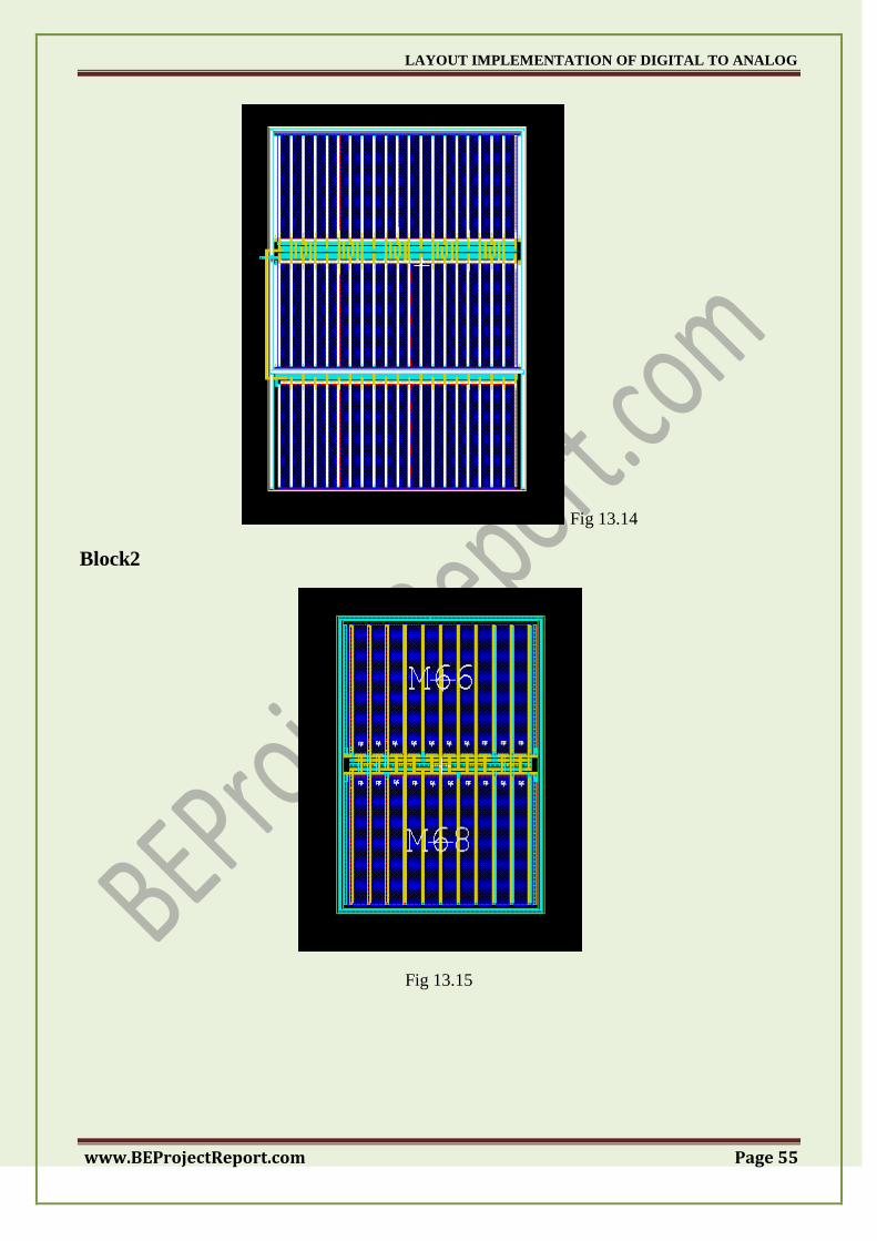
LAYOUT IMPLEMENTATION OF DIGITAL TO ANALOG
www.BEProjectReport.com Page 55
Fig 13.14
Block2
Fig 13.15

LAYOUT IMPLEMENTATION OF DIGITAL TO ANALOG
www.BEProjectReport.com Page 56
12.8 BIAS GENERATOR - FOR THE OPERATIONAL AMPLIFIER
Schematic:
Fig 13.16
Layout:
Fig 13.17

LAYOUT IMPLEMENTATION OF DIGITAL TO ANALOG
www.BEProjectReport.com Page 57
12.9 BASIC RESISTANCE:
Fig 13.18
12.10 CAPACITANCE BLOCK:
Fig 13.19
LAYOUT IMPLEMENTATION OF DIGITAL TO ANALOG
www.BEProjectReport.com Page 58
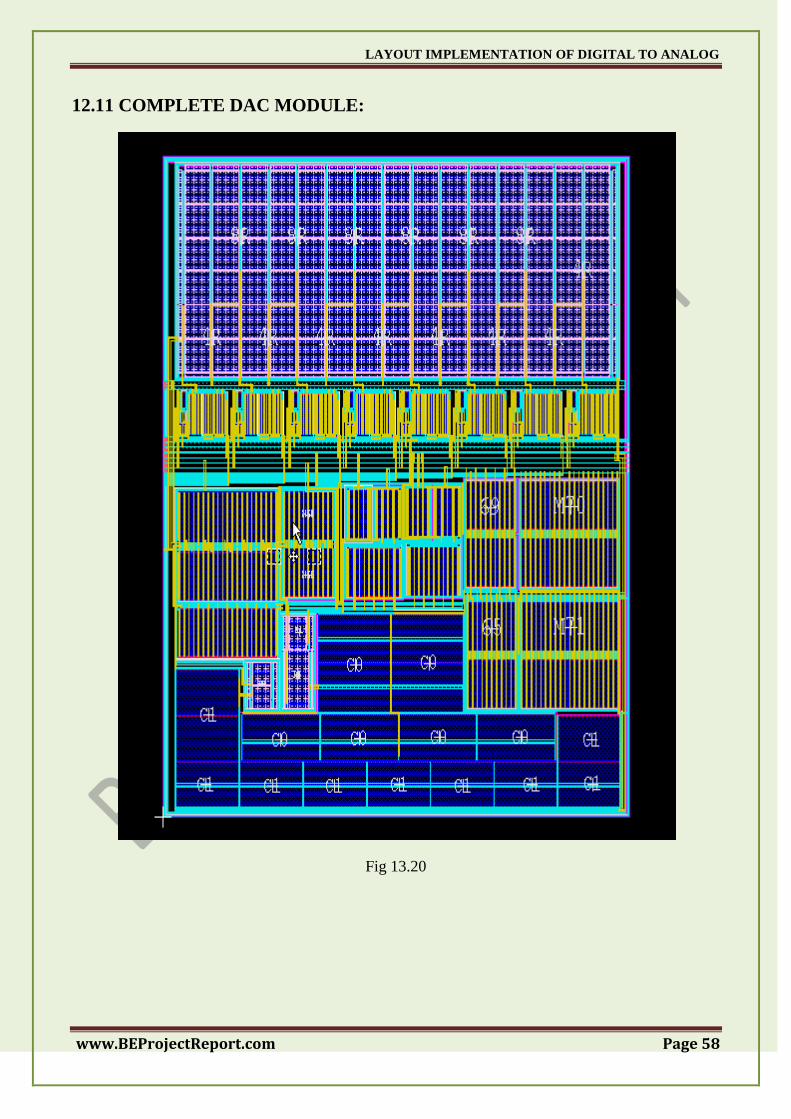
12.11 COMPLETE DAC MODULE:
Fig 13.20
LAYOUT IMPLEMENTATION OF DIGITAL TO ANALOG
www.BEProjectReport.com Page 59
12.12 DRC REPORT FOR COMPLETE MODULE:
With density errors:
Fig 13.21
Density errors cleared:
Fig 13.21

LAYOUT IMPLEMENTATION OF DIGITAL TO ANALOG
www.BEProjectReport.com Page 60
LVS report:
Fig 13.22
SUMMARY
The complete schematic diagram of R-2R ladder DAC is divided into sub modules and
layout is drawn for each and every module DRC and LVS are cleared for each module using
TANNER EDA Tool and TSMC 0.13um technology, then every module is clubbed together to get
final module, and now DRC and LVS is cleared for final DAC layout the given specifications.

LAYOUT IMPLEMENTATION OF DIGITAL TO ANALOG
www.BEProjectReport.com Page 61
APPENDIX-A
HANDS ON TANNER EDA TOOL
1.1 GATE LAYOUT:
Layout can be very time consuming
Design gates to fit together nicely
Build a library of standard cells
Standard cell design methodology
VDD and GND should abut (standard height)
Adjacent gates should satisfy design rules
nMOS at bottom and pMOS at top
All gates include well and substrate contacts
1.2 GUIDELINES FOR STANDARD CELL LAYOUTS
1) All The Standard cells should be of the same height.
2) Routing within the cell should be done either with POLY or metal1.
3) Cell Width should be multiples of via to line pitch
4) The power and ground straps should be designed so that they can be shared with cells placed
above/below.
5) The cell boundary should also be multiples of via to line pitch
6) The I/P and O/P pins should be placed evenly throughout the cell and can be placed at half of
the via to line pitch
1.3 IC LAYOUT EDITOR:
An Integrated circuit layout editor or IC layout editor is an electronic design automation
software tool that allows a user to digitize the shapes and patterns that form an integrated circuit.
Typically the view will include the components (usually as pcells), metal routing tracks,
Via(electronics) and electrical pins. Software of this type is similar to computer aided drafting
software, but is specialized for the task of integrated circuit layout.
1.4 THE TYPICAL FLOW FOR THE LAYOUT OF ANALOG CIRCUITS
MIGHT BE:
1. The layout engineer receives the schematic from the designer in electrical form
2. Either the tool or the layout engineer creates a physical view of the circuit including all of the
required components and electrical pins
3. The layout engineer positions the components to minimize both the area required and the
negative effects of layout parasitics upon the circuit performance and also to allow good
routing to neighboring cells

LAYOUT IMPLEMENTATION OF DIGITAL TO ANALOG
www.BEProjectReport.com Page 62
4. The layout engineer uses metal routing to connect all of the components, again taking care to
avoid unwanted layout parasitic on critical nodes
5. The layout engineer uses DRC and LVS checks to ensure that the circuit is both
manufacturable and functional
In some cases the layout engineer will request minor changes to the schematic to simplify the layout.
1.5 INTRODUCTION TO LAYOUT EDITING (TANNER L-EDIT)
Launching L-Edit:
To launch L-Edit, click the Start button on the Windows taskbar and navigate to the L-Edit
directory in the Tanner EDA directory. You can also double-click the L-Edit icon on your desktop,
which looks like this:
Setup Files:
Every L-Edit design file contains basic information such as a layer list, technology settings,
and module-specific options for SPR, DRC, and Extract. Collectively, this information is known as
the ―setup.‖ You can transfer this information between design files using File > Replace Setup and
File > Export Setup. See ―Application and Design Setup‖ on page 75 for further information. When
you launch L-Edit, the program attempts to locate the file ledit.tdb and read it for setup information.
If it does not find this file in the current directory, L-Edit searches the directory where the executable
is located. If L-Edit does not locate ledit.tdb, it displays a warning. With or without setup
information from ledit.tdb, when L-Edit launches it creates a new file (Layout1) with one cell, Cell0.
To start L-Edit with a specific TDB file, double-click the TDB file in Windows Explorer.
Command-Line Arguments:
L-Edit may be launched with or without command-line arguments. If a command-line TDB
File is not specified in the command line, L-Edit starts with a new empty layout file modeled after
ledit.tdb. To launch L-Edit with a command-line argument, click the Start button on the Windows
taskbar and select Run. Use the Browse button and navigate to the directory that contains ledit.exe.
Command line options can also be
put into a program shortcut by
editing the shortcut properties.
Elements of the User Interface:
The application interface is
displayed on the next page. Each
of the components is described in
the Following sections.
Title Bar and Menu Bar
The title bar indicates the active
file and cell. The menu bar, the
horizontal space at the top of the

LAYOUT IMPLEMENTATION OF DIGITAL TO ANALOG
www.BEProjectReport.com Page 63
screen, contains the titles of the L-Edit command menus.
File: Commands for creating, opening, saving, and printing files
Edit: Commands for copying, deleting, selecting, finding, and textual editing
View: Commands for expanding, contracting, and shifting the view
Draw: Commands for transforming design elements
Cell: Commands for creating, manipulating, and instancing cells
Setup: Commands for customizing setup parameters for the application, design, layers,
color palette, and tools
Tools: Commands for examining XrefCells, creating and clearing generated layers,
DRC, placing and routing the design, extracting a netlist, viewing a cross-section, and running L-
Edit macros
Window: Commands for displaying document windows
Help: Commands for accessing online user guides and general information about L-Edit
and Tanner EDA
Layer Palettes: L-Edit supports an unlimited number of technology layers. They can be
displayed using either of two layer ―palettes.‖ The Compact Layer Palette, a grid of icons that
replicate each layer‘s color and pattern, provides a quick way to select layers. The Layer Palette is
also used for layer selection, but provides additional features for layer display and manipulation.
Either or both palettes can be open at once, and can float or be docked. You can resize the palettes or
use the scroll bars to view layers not visible in the current display. Both can be filtered using a pull-
down category list to display just those layers that are just those Drawn, In Use, Generated or Special.
You can also select Filter then enter text in the entry field to limit display to layers that include the
exactly the characters entered, anywhere in the layer name.
Working with Files:
Files
A complete L-Edit design is composed of cells contained in a design file. You can open as many
design files simultaneously as your hardware allows. The name of the active file appears in the L-
Edit title bar.
Creating Files
Create new files by choosing File > New, which opens the New File dialog:
LAYOUT IMPLEMENTATION OF DIGITAL TO ANALOG
www.BEProjectReport.com Page 64
L-Edit will open a layout window or the Tanner text editor, depending upon the file type you have
selected. You can also drag and drop a text file into the layout window to open it. If you use the right
mouse button to drag and drop the file, you can open a text file as a specific type. L-Edit will prompt
you to indicate the document type and also show the expected type in a bold font.
Options include:
Setup Files
The list of predefined setup files will contain:
<empty>—this is a standard empty setup (this is the default setup with white background, single
layer and no DRC rules).
The list of currently loaded TDB files (displayed in bold face).
The list of TDB setup files found in the predefined setup directories. You can specify the TDB setup
path in the Setup Application dialog. When you create a new file, L-Edit will assign it a default name
(ex. Text or Spice), followed by a number, e.g., Text2 or Spice5, depending on the history of the
current session. When you first save the new file, you will be prompted to change the filename, if
needed.
TDB File Format
Tanner Database (TDB) is a proprietary, machine-readable format optimized for the Tanner
Tools environment. TDB files are saved with the .tdb filename extension. By default, the scrollable
list displays TDB files.Along with the design itself, a TDB file contains setup information including
layer rendering information, CIF and GDSII setup information, design rules, and L-Edit
configuration settings. Setup information can be read into L-Edit with File > Replace Setup.When a
file is saved, L-Edit automatically backs up previously-saved versions of the file with a .tdo
extension.
LAYOUT IMPLEMENTATION OF DIGITAL TO ANALOG
www.BEProjectReport.com Page 65
Application and Design Setup
Replacing the Setup
Every L-Edit design file contains basic information such as a layer list, technology settings, and
module-specific options for SPR, DRC, and Extract. Collectively, this information is known as the
―setup.‖
File > Replace Setup transfers setup information from a file (the source file) to the current file (the
destination file).Options include:
From file: Name of the TDB file whose setup is to be imported. Click Browse to navigate to an
existing file.
Layers: Imports layer setup from the specified file.
Replace deletes the layers in the destination file and replaces them with the layers from the
source file.
Merge adds the layers from the source file to the list of available layers in the destination file.
Source file layers not present in the destination file are appended to the layer list in the
destination file. If a layer in the source file has the same name as a layer in the destination file,
the position it has in the destination file is maintained.
Additional layer-specific setup options include:
CIF names
GDS II numbers
Wire settings

LAYOUT IMPLEMENTATION OF DIGITAL TO ANALOG
www.BEProjectReport.com Page 66
Technology Options include:
Maintain physical size—With this option, L-Edit checks all objects in all cells and unit-
specific parameters entered in other dialogs to determine if the layout will be truncated when
it is rescaled. L-Edit presents one warning for each cell and set of parameters if a truncation
will occur. If you answer yes to all the warnings, or if no truncation will occur, L-Edit
rescales the design. If you answer No to any of the warnings, L-Edit cancels the rescaling
operation.
Rescale—L-Edit rescales the design by applying technology scaling parameters in the source
file to objects in the destination file.
Draw Transfers the parameters entered in Setup Design—Drawing.
Palette Transfers the color parameters entered in Setup Colors.
Show/Hides Transfers the view settings for grid, origin, ports, and other objects.
Properties If checked, replaces the System and other parameters set in File > Info>Properties.
Selection Transfers the parameters entered in Setup Design—Selection.
Grid Transfers the parameters for the display grid and mouse snap grid.
Xref files If checked, replaces the TDB files that will be used as cross-reference
of library files, as set in Setup > Design—Xref files.
Modules Check the corresponding box to replace setup information for:
DRC rules
Extract
Cross-Section
SPR: Check the corresponding box to replace setup information for
Core setup (see SPR Core Setup on page 354)
Pad frame setup (see SPR Pad frame Setup on page 365)
Pad route setup (see SPR Pad Route Setup on page 369)
Place and Route configuration (see SPR Setup on page 351)
Uncheck All Deselects all options
Importing a Setup from Virtuoso
This import feature simplifies transitions of designs from the Cadence Virtuoso to the Tanner L-Edit
design environment. Importing a Virtuoso setup always creates a new L-Edit file. The display and
tech files are concatenated and read as one.
The Setup > Import Virtuoso® Setup command creates an L-Edit technology setup by reading a
Virtuoso technology file. Imported elements include palette colors, background color, grid colors,
layers (including rendering information, GDS layer number and GDS datatype) and manufacturing
grid. L-Edit elements that are missing from Virtuoso (such as user-defined rendering) are
automatically generated.

LAYOUT IMPLEMENTATION OF DIGITAL TO ANALOG
www.BEProjectReport.com Page 67
Display file Specifies rendering information (palette colors and stipple patterns.)
Tech file: Specifies technology information (layers, purposes, and bindings
between these and display data).
Display name: In Virtuoso, ―displays‖ are used to identify particular drawing styles, often optimized
for specific display devices (e.g., screen, plotter, printer). One of these displays must be selected to
import into L-Edit.
Create L-Edit layers from: L-Edit layers can be created from any of three sources:
Virtuoso tech Layers/tech Purposes—An L-Edit layer can be created or each pair of Virtuoso layer
/ purpose. A Virtuoso ―purpose‖ identifies an application of a given layer; for example, layer ―metal‖
can have two purposes: ―contact‖ and ―wire‖. Each layer-purpose pair has its own rendering
information, GDS number, etc.
Virtuoso Tech Layers (in Tech Display order): An L-Edit layer can be created for
Each Virtuoso layer. The renderin information is taken from the first packet bound to that layer,
for the particular display specified.
Virtuoso packets—Rendering information in Virtuoso (line styles, colors and weights, fill colors
and stipples) is grouped into ―packets‖. An L-Edit layer can be created for each Virtuoso packet.
Merging Layer Setups
When you merge layer setups, L-Edit adds source-file layers to the layer list in the destination file. If
the source file has layers not present in the destination file, L-Edit appends them to the destination-
file layer list. If the source file and destination file have a layer with the same name, the layer
maintains its position in the destination file‘s layer list.
For example, a source file contains layers A, B, and C (in that order), and a destination file contains
layers B, D, and E (in that order). After replacing, the destination file will contain layers A, B, and C.

LAYOUT IMPLEMENTATION OF DIGITAL TO ANALOG
www.BEProjectReport.com Page 68
After merging, the destination file will contain layers B, D, E, A, and C. (The destination file‘s
information on layer B is replaced with the source file‘s information on layer B.)
________________________________________________________________________
Note: Importing a layer setup also transfers a layer‘s lock status from the source file to the target file.
For example, if you lock Metal1 in the source file, it will be locked in the target file. Conversely, if
you lock Metal1 in the target file but unlock it in the source file, it will then be unlocked in the target
file after you replace the layer setup.
Color Parameters
You can display an L-Edit design file using 16, 32, 64, 128, or 256 colors in your palette. You use
the
Setup > Colors command to set the number of and RGB definition of your design colors.
Each color has two attributes, a unique identifying binary code and an RGB color definition. The
Setup
Colors dialog provides the following options:
Number of colors: Select the number of colors that will be available for defining layer colors.
Options are 16, 32, 64, 128, or 256 (True Color mode) colors.
Sort colors by: Select how colors will be sorted. This setting applies to both this dialog and the
Setup Layers dialog.
Options are:
Index: sorts by index number, which is the binary value of a color.
Number of bits: sorts by the number of bits used to define a color and then by index number if the
number of bits set are equal.
Hue: sorts by hue, then saturation, then luminosity, then index number.
Brightness: sorts by luminosity in descending order, then hue, then saturation, then index number.
(Left pane) Shows a sample of each defined color and the associated 4- to 8- bit binary code used to
LAYOUT IMPLEMENTATION OF DIGITAL TO ANALOG
www.BEProjectReport.com Page 69
assign a unique color index number to that color. The number of bits used in each color depends on
the number of colors available in the file (for example, 4 bits are used in a 16 color file).
Color (RGB): Displays the composition of each color as a function of its Red, Green, and Blue
values, which can range from 0 to 255. You can use the slider controls or type a number in the red,
green and blue colored boxes to modify a color.
Color Picker: Opens the standard Windows Color dialog that allows you to select and
define colors.
Application Parameters: To modify application-level settings in L-Edit, choose Setup >
Application. Application-level settings are divided into nine categories, which appear on separate
tabs. General, Keyboard, Mouse, Warnings, UPI, Rendering, Selection, Text Editor and Text Style.
Configuration Files: Application settings are saved in application configuration (.ini)
files. You specify configuration file options in the top portion of the
Setup Application dialog. Configuration files are ASCII files containing
application-wide setup information that can be edited and shared among multiple users. To load
settings from an existing file, enter the name of the file in the Workgroup or User field, or choose
from available files using the Browse
button next to the desired field. Click
Load to load the settings into L-Edit.
Workgroup and User Configuration
Files
L-Edit can load configuration
information from either a Workgroup or a User file. Workgroup files are intended to be shared by
multiple users; for example, they may contain key remapping sequences that will be used by many
users. User files are intended to contain preferences specific to a particular individual. Changes in the
Setup Application dialog can only be saved to User configuration files. Therefore, an INI file loaded
as a Workgroup file is protected from accidentally being changed. When both workgroup and user
files are specified in Setup Application, settings from the user file override settings in the workgroup
file. To create a workgroup configuration file, first save the desired settings in a user configuration
file. You can then copy the user configuration file to a new name to create a workgroup file.
LAYOUT IMPLEMENTATION OF DIGITAL TO ANALOG
www.BEProjectReport.com Page 70
BIBLIOGRAPHY
1. CMOS IC Layout Concepts, methodologies and tools-Dan Clein
Technical Contributor: Gregg Shimokura
2. Stick diagram fundamentals-John P.Uyemura.
3. The art of analog layouts-Allen Hastings
4. Principles of CMOS VLSI design- Neil weste.
5. T. E. Dillinger, VLSI Engineering, Englewood Cliffs, NJ: Prentice-Hall, Inc., 1988.
6. S.M. Sze, VLSI Technology, New York, NY: McGraw-Hill, 1983.
7. Dr. Paul D. Franzon, www.ece.ncsu.edu/erl/faculty/paulf.html
8. Sung Kang and Yusuf Leblebici, CMOS Digital Integrated Circuits, 3rd edition, McGraw-Hill,
2004
9.R. Jacob Baker, CMOS Circuit Design, Layout, and Simulation, 2nd edition, IEEE Press, 2005
10. Dan Clein, CMOS IC Layout: Concept, Methodologies and Tools, Newnes, 1999
11. Alan Hastings, Art of Analog Layout, 2nd edition, Prentice Hall, 2005
12. Alan Hastings, Art of Analog Layout, 2nd edition, Prentice Hall, 2005
13 http://www.end.utah.edu/browen/
14 http://ami.ac.uk/
15 http://www.epfl.eh/lsi2001/