d TL494 Expl
31
Application Report SLVA001C - December 2003 - Revised August 2004 1 ` Designing Switching Voltage Regulators With the TL494 Patrick Griffith Standard Linear & Logic ABSTRACT The TL494 power-supply controller is discussed in detail. A general overview of the TL494 architecture presents the primary functional blocks contained in the device. An in-depth study of the interrelationship between the functional blocks highlights versatility and limitations of the TL494. The usefulness of the TL494 power-supply controller also is demonstrated through several basic applications, and a design example is included for a 5-V/10-A power supply. Contents Introduction 4 . . . . . . . . . . . . . . . . . . . . . . . . . . . . . . . . . . . . . . . . . . . . . . . . . . . . . . . . . . . . . . . . . . . . . . . . . . . . . The Basic Device 4 . . . . . . . . . . . . . . . . . . . . . . . . . . . . . . . . . . . . . . . . . . . . . . . . . . . . . . . . . . . . . . . . . . . . . . . . . Principle of Operation 5 . . . . . . . . . . . . . . . . . . . . . . . . . . . . . . . . . . . . . . . . . . . . . . . . . . . . . . . . . . . . . . . . . . . . 5-V Reference Regulator 5 . . . . . . . . . . . . . . . . . . . . . . . . . . . . . . . . . . . . . . . . . . . . . . . . . . . . . . . . . . . . . . Oscillator 7 . . . . . . . . . . . . . . . . . . . . . . . . . . . . . . . . . . . . . . . . . . . . . . . . . . . . . . . . . . . . . . . . . . . . . . . . . . . . Operation Frequency 7 . . . . . . . . . . . . . . . . . . . . . . . . . . . . . . . . . . . . . . . . . . . . . . . . . . . . . . . . . . . . . Operation Above 150 kHz 8 . . . . . . . . . . . . . . . . . . . . . . . . . . . . . . . . . . . . . . . . . . . . . . . . . . . . . . . . . Dead-Time Control/PWM Comparator 9 . . . . . . . . . . . . . . . . . . . . . . . . . . . . . . . . . . . . . . . . . . . . . . . . . . . Dead-Time Control 9 . . . . . . . . . . . . . . . . . . . . . . . . . . . . . . . . . . . . . . . . . . . . . . . . . . . . . . . . . . . . . . . Comparator 10 . . . . . . . . . . . . . . . . . . . . . . . . . . . . . . . . . . . . . . . . . . . . . . . . . . . . . . . . . . . . . . . . . . . . . Pulse-Width Modulation (PWM) 10 . . . . . . . . . . . . . . . . . . . . . . . . . . . . . . . . . . . . . . . . . . . . . . . . . . . Error Amplifiers 10 . . . . . . . . . . . . . . . . . . . . . . . . . . . . . . . . . . . . . . . . . . . . . . . . . . . . . . . . . . . . . . . . . Output-Control Logic 13 . . . . . . . . . . . . . . . . . . . . . . . . . . . . . . . . . . . . . . . . . . . . . . . . . . . . . . . . . . . . . . . . . Output-Control Input 13 . . . . . . . . . . . . . . . . . . . . . . . . . . . . . . . . . . . . . . . . . . . . . . . . . . . . . . . . . . . . . Pulse-Steering Flip-Flop 14 . . . . . . . . . . . . . . . . . . . . . . . . . . . . . . . . . . . . . . . . . . . . . . . . . . . . . . . . . . Output Transistors 14 . . . . . . . . . . . . . . . . . . . . . . . . . . . . . . . . . . . . . . . . . . . . . . . . . . . . . . . . . . . . . . . . . . . Applications 16 . . . . . . . . . . . . . . . . . . . . . . . . . . . . . . . . . . . . . . . . . . . . . . . . . . . . . . . . . . . . . . . . . . . . . . . . . . . . Reference Regulator 16 . . . . . . . . . . . . . . . . . . . . . . . . . . . . . . . . . . . . . . . . . . . . . . . . . . . . . . . . . . . . . . . . . Current Boosting the 5-V Regulator 16 . . . . . . . . . . . . . . . . . . . . . . . . . . . . . . . . . . . . . . . . . . . . . . . . Applications of the Oscillator 17 . . . . . . . . . . . . . . . . . . . . . . . . . . . . . . . . . . . . . . . . . . . . . . . . . . . . . . . . . . Synchronization 17 . . . . . . . . . . . . . . . . . . . . . . . . . . . . . . . . . . . . . . . . . . . . . . . . . . . . . . . . . . . . . . . . . Master/Slave Synchronization 17 . . . . . . . . . . . . . . . . . . . . . . . . . . . . . . . . . . . . . . . . . . . . . . . . . . . . . Master Clock Operation 17 . . . . . . . . . . . . . . . . . . . . . . . . . . . . . . . . . . . . . . . . . . . . . . . . . . . . . . . . . . Fail-Safe Operation 18 . . . . . . . . . . . . . . . . . . . . . . . . . . . . . . . . . . . . . . . . . . . . . . . . . . . . . . . . . . . . . . Error-Amplifier-Bias Configuration 19 . . . . . . . . . . . . . . . . . . . . . . . . . . . . . . . . . . . . . . . . . . . . . . . . . . . . . . Current Limiting 19 . . . . . . . . . . . . . . . . . . . . . . . . . . . . . . . . . . . . . . . . . . . . . . . . . . . . . . . . . . . . . . . . . . . . . . Fold-Back Current Limiting 19 . . . . . . . . . . . . . . . . . . . . . . . . . . . . . . . . . . . . . . . . . . . . . . . . . . . . . . . . Pulse-Current Limiting 20 . . . . . . . . . . . . . . . . . . . . . . . . . . . . . . . . . . . . . . . . . . . . . . . . . . . . . . . . . . . Trademarks are the property of their respective owners.
-
Upload
erick-depthios -
Category
Documents
-
view
55 -
download
4
description
a
Transcript of d TL494 Expl
Application ReportSLVA001C - December 2003 − Revised August 2004
1
Designing Switching Voltage Regulators With the TL494
Patrick Griffith Standard Linear & Logic
ABSTRACT
The TL494 power-supply controller is discussed in detail. A general overview of the TL494architecture presents the primary functional blocks contained in the device. An in-depth studyof the interrelationship between the functional blocks highlights versatility and limitations ofthe TL494. The usefulness of the TL494 power-supply controller also is demonstratedthrough several basic applications, and a design example is included for a 5-V/10-A powersupply.
Contents
Introduction 4. . . . . . . . . . . . . . . . . . . . . . . . . . . . . . . . . . . . . . . . . . . . . . . . . . . . . . . . . . . . . . . . . . . . . . . . . . . . .
The Basic Device 4. . . . . . . . . . . . . . . . . . . . . . . . . . . . . . . . . . . . . . . . . . . . . . . . . . . . . . . . . . . . . . . . . . . . . . . . .
Principle of Operation 5. . . . . . . . . . . . . . . . . . . . . . . . . . . . . . . . . . . . . . . . . . . . . . . . . . . . . . . . . . . . . . . . . . . . 5-V Reference Regulator 5. . . . . . . . . . . . . . . . . . . . . . . . . . . . . . . . . . . . . . . . . . . . . . . . . . . . . . . . . . . . . . Oscillator 7. . . . . . . . . . . . . . . . . . . . . . . . . . . . . . . . . . . . . . . . . . . . . . . . . . . . . . . . . . . . . . . . . . . . . . . . . . . .
Operation Frequency 7. . . . . . . . . . . . . . . . . . . . . . . . . . . . . . . . . . . . . . . . . . . . . . . . . . . . . . . . . . . . . Operation Above 150 kHz 8. . . . . . . . . . . . . . . . . . . . . . . . . . . . . . . . . . . . . . . . . . . . . . . . . . . . . . . . .
Dead-Time Control/PWM Comparator 9. . . . . . . . . . . . . . . . . . . . . . . . . . . . . . . . . . . . . . . . . . . . . . . . . . . Dead-Time Control 9. . . . . . . . . . . . . . . . . . . . . . . . . . . . . . . . . . . . . . . . . . . . . . . . . . . . . . . . . . . . . . . Comparator 10. . . . . . . . . . . . . . . . . . . . . . . . . . . . . . . . . . . . . . . . . . . . . . . . . . . . . . . . . . . . . . . . . . . . . Pulse-Width Modulation (PWM) 10. . . . . . . . . . . . . . . . . . . . . . . . . . . . . . . . . . . . . . . . . . . . . . . . . . . Error Amplifiers 10. . . . . . . . . . . . . . . . . . . . . . . . . . . . . . . . . . . . . . . . . . . . . . . . . . . . . . . . . . . . . . . . .
Output-Control Logic 13. . . . . . . . . . . . . . . . . . . . . . . . . . . . . . . . . . . . . . . . . . . . . . . . . . . . . . . . . . . . . . . . . Output-Control Input 13. . . . . . . . . . . . . . . . . . . . . . . . . . . . . . . . . . . . . . . . . . . . . . . . . . . . . . . . . . . . . Pulse-Steering Flip-Flop 14. . . . . . . . . . . . . . . . . . . . . . . . . . . . . . . . . . . . . . . . . . . . . . . . . . . . . . . . . .
Output Transistors 14. . . . . . . . . . . . . . . . . . . . . . . . . . . . . . . . . . . . . . . . . . . . . . . . . . . . . . . . . . . . . . . . . . .
Applications 16. . . . . . . . . . . . . . . . . . . . . . . . . . . . . . . . . . . . . . . . . . . . . . . . . . . . . . . . . . . . . . . . . . . . . . . . . . . . Reference Regulator 16. . . . . . . . . . . . . . . . . . . . . . . . . . . . . . . . . . . . . . . . . . . . . . . . . . . . . . . . . . . . . . . . .
Current Boosting the 5-V Regulator 16. . . . . . . . . . . . . . . . . . . . . . . . . . . . . . . . . . . . . . . . . . . . . . . . Applications of the Oscillator 17. . . . . . . . . . . . . . . . . . . . . . . . . . . . . . . . . . . . . . . . . . . . . . . . . . . . . . . . . .
Synchronization 17. . . . . . . . . . . . . . . . . . . . . . . . . . . . . . . . . . . . . . . . . . . . . . . . . . . . . . . . . . . . . . . . . Master/Slave Synchronization 17. . . . . . . . . . . . . . . . . . . . . . . . . . . . . . . . . . . . . . . . . . . . . . . . . . . . . Master Clock Operation 17. . . . . . . . . . . . . . . . . . . . . . . . . . . . . . . . . . . . . . . . . . . . . . . . . . . . . . . . . . Fail-Safe Operation 18. . . . . . . . . . . . . . . . . . . . . . . . . . . . . . . . . . . . . . . . . . . . . . . . . . . . . . . . . . . . . .
Error-Amplifier-Bias Configuration 19. . . . . . . . . . . . . . . . . . . . . . . . . . . . . . . . . . . . . . . . . . . . . . . . . . . . . . Current Limiting 19. . . . . . . . . . . . . . . . . . . . . . . . . . . . . . . . . . . . . . . . . . . . . . . . . . . . . . . . . . . . . . . . . . . . . .
Fold-Back Current Limiting 19. . . . . . . . . . . . . . . . . . . . . . . . . . . . . . . . . . . . . . . . . . . . . . . . . . . . . . . . Pulse-Current Limiting 20. . . . . . . . . . . . . . . . . . . . . . . . . . . . . . . . . . . . . . . . . . . . . . . . . . . . . . . . . . .
Trademarks are the property of their respective owners.
SLVA001C
2 Designing Switching Voltage Regulators With the TL494
Applications of the Dead-Time Control 22. . . . . . . . . . . . . . . . . . . . . . . . . . . . . . . . . . . . . . . . . . . . . . . . . . Soft Start 22. . . . . . . . . . . . . . . . . . . . . . . . . . . . . . . . . . . . . . . . . . . . . . . . . . . . . . . . . . . . . . . . . . . . . . . Overvoltage Protection 23. . . . . . . . . . . . . . . . . . . . . . . . . . . . . . . . . . . . . . . . . . . . . . . . . . . . . . . . . . . Modulation of Turnon/Turnoff Transition 23. . . . . . . . . . . . . . . . . . . . . . . . . . . . . . . . . . . . . . . . . . . .
Design Example 25. . . . . . . . . . . . . . . . . . . . . . . . . . . . . . . . . . . . . . . . . . . . . . . . . . . . . . . . . . . . . . . . . . . . . . . . . Input Power Source 25. . . . . . . . . . . . . . . . . . . . . . . . . . . . . . . . . . . . . . . . . . . . . . . . . . . . . . . . . . . . . . . . . . Control Circuits 26. . . . . . . . . . . . . . . . . . . . . . . . . . . . . . . . . . . . . . . . . . . . . . . . . . . . . . . . . . . . . . . . . . . . . .
Oscillator 26. . . . . . . . . . . . . . . . . . . . . . . . . . . . . . . . . . . . . . . . . . . . . . . . . . . . . . . . . . . . . . . . . . . . . . . Error Amplifier 27. . . . . . . . . . . . . . . . . . . . . . . . . . . . . . . . . . . . . . . . . . . . . . . . . . . . . . . . . . . . . . . . . . Current-Limiting Amplifier 27. . . . . . . . . . . . . . . . . . . . . . . . . . . . . . . . . . . . . . . . . . . . . . . . . . . . . . . . . Soft Start and Dead Time 28. . . . . . . . . . . . . . . . . . . . . . . . . . . . . . . . . . . . . . . . . . . . . . . . . . . . . . . . .
Inductor Calculations 29. . . . . . . . . . . . . . . . . . . . . . . . . . . . . . . . . . . . . . . . . . . . . . . . . . . . . . . . . . . . . . . . . Output Capacitance Calculations 29. . . . . . . . . . . . . . . . . . . . . . . . . . . . . . . . . . . . . . . . . . . . . . . . . . . . . . Transistor Power-Switch Calculations 30. . . . . . . . . . . . . . . . . . . . . . . . . . . . . . . . . . . . . . . . . . . . . . . . . . .
List of Figures
1. TL494 Block Diagram 4. . . . . . . . . . . . . . . . . . . . . . . . . . . . . . . . . . . . . . . . . . . . . . . . . . . . . . . . . . . . . . . . . . 2. TL494 Modulation Technique 5. . . . . . . . . . . . . . . . . . . . . . . . . . . . . . . . . . . . . . . . . . . . . . . . . . . . . . . . . . . 3. 5-V Reference Regulator 6. . . . . . . . . . . . . . . . . . . . . . . . . . . . . . . . . . . . . . . . . . . . . . . . . . . . . . . . . . . . . . . 4. Reference Voltage vs Input Voltage 6. . . . . . . . . . . . . . . . . . . . . . . . . . . . . . . . . . . . . . . . . . . . . . . . . . . . . . 5. Internal-Oscillator Schematic 7. . . . . . . . . . . . . . . . . . . . . . . . . . . . . . . . . . . . . . . . . . . . . . . . . . . . . . . . . . . . 6. Oscillator Frequency vs RT/CT 8. . . . . . . . . . . . . . . . . . . . . . . . . . . . . . . . . . . . . . . . . . . . . . . . . . . . . . . . . . 7. Variation of Dead Time vs RT/CT 8. . . . . . . . . . . . . . . . . . . . . . . . . . . . . . . . . . . . . . . . . . . . . . . . . . . . . . . . 8. Dead-Time Control/PWM Comparator 9. . . . . . . . . . . . . . . . . . . . . . . . . . . . . . . . . . . . . . . . . . . . . . . . . . . . 9. Error Amplifiers 11. . . . . . . . . . . . . . . . . . . . . . . . . . . . . . . . . . . . . . . . . . . . . . . . . . . . . . . . . . . . . . . . . . . . . .
10. Multiplex Structure of Error Amplifiers 11. . . . . . . . . . . . . . . . . . . . . . . . . . . . . . . . . . . . . . . . . . . . . . . . . . . 11. Error-Amplifier-Bias Configurations for Controlled-Gain Applications 12. . . . . . . . . . . . . . . . . . . . . . . . 12. Amplifier Transfer Characteristics 12. . . . . . . . . . . . . . . . . . . . . . . . . . . . . . . . . . . . . . . . . . . . . . . . . . . . . . . 13. Amplifier Bode Plot 12. . . . . . . . . . . . . . . . . . . . . . . . . . . . . . . . . . . . . . . . . . . . . . . . . . . . . . . . . . . . . . . . . . . 14. Output-Steering Architecture 13. . . . . . . . . . . . . . . . . . . . . . . . . . . . . . . . . . . . . . . . . . . . . . . . . . . . . . . . . . . 15. Pulse-Steering Flip-Flop 14. . . . . . . . . . . . . . . . . . . . . . . . . . . . . . . . . . . . . . . . . . . . . . . . . . . . . . . . . . . . . . . 16. Output-Transistor Structure 15. . . . . . . . . . . . . . . . . . . . . . . . . . . . . . . . . . . . . . . . . . . . . . . . . . . . . . . . . . . . 17. Conventional Three-Terminal Regulator Current-Boost Technique 16. . . . . . . . . . . . . . . . . . . . . . . . . . 18. TL494 Reference Regulator Current-Boost Technique 16. . . . . . . . . . . . . . . . . . . . . . . . . . . . . . . . . . . . . 19. Master/Slave Synchronization 17. . . . . . . . . . . . . . . . . . . . . . . . . . . . . . . . . . . . . . . . . . . . . . . . . . . . . . . . . . 20. External Clock Synchronization 18. . . . . . . . . . . . . . . . . . . . . . . . . . . . . . . . . . . . . . . . . . . . . . . . . . . . . . . . 21. Oscillator Start-Up Circuit 18. . . . . . . . . . . . . . . . . . . . . . . . . . . . . . . . . . . . . . . . . . . . . . . . . . . . . . . . . . . . . . 22. Fail-Safe Protection 18. . . . . . . . . . . . . . . . . . . . . . . . . . . . . . . . . . . . . . . . . . . . . . . . . . . . . . . . . . . . . . . . . . . 23. Error-Amplifier-Bias Configurations 19. . . . . . . . . . . . . . . . . . . . . . . . . . . . . . . . . . . . . . . . . . . . . . . . . . . . . 24. Fold-Back Current Limiting 19. . . . . . . . . . . . . . . . . . . . . . . . . . . . . . . . . . . . . . . . . . . . . . . . . . . . . . . . . . . . 25. Fold-Back Current Characteristics 20. . . . . . . . . . . . . . . . . . . . . . . . . . . . . . . . . . . . . . . . . . . . . . . . . . . . . . 26. Error-Signal Considerations 21. . . . . . . . . . . . . . . . . . . . . . . . . . . . . . . . . . . . . . . . . . . . . . . . . . . . . . . . . . .

SLVA001C
3 Designing Switching Voltage Regulators With the TL494
27. Peak-Current Protection 21. . . . . . . . . . . . . . . . . . . . . . . . . . . . . . . . . . . . . . . . . . . . . . . . . . . . . . . . . . . . . . . 28. Dead-Time Control Characteristics 22. . . . . . . . . . . . . . . . . . . . . . . . . . . . . . . . . . . . . . . . . . . . . . . . . . . . . 29. Tailored Dead Time 22. . . . . . . . . . . . . . . . . . . . . . . . . . . . . . . . . . . . . . . . . . . . . . . . . . . . . . . . . . . . . . . . . . . 30. Soft-Start Circuit 23. . . . . . . . . . . . . . . . . . . . . . . . . . . . . . . . . . . . . . . . . . . . . . . . . . . . . . . . . . . . . . . . . . . . . 31. Overvoltage-Protection Circuit 23. . . . . . . . . . . . . . . . . . . . . . . . . . . . . . . . . . . . . . . . . . . . . . . . . . . . . . . . . 32. Turnon Transition 24. . . . . . . . . . . . . . . . . . . . . . . . . . . . . . . . . . . . . . . . . . . . . . . . . . . . . . . . . . . . . . . . . . . . . 33. Turnoff Transition 24. . . . . . . . . . . . . . . . . . . . . . . . . . . . . . . . . . . . . . . . . . . . . . . . . . . . . . . . . . . . . . . . . . . . . 34. Input Power Source 25. . . . . . . . . . . . . . . . . . . . . . . . . . . . . . . . . . . . . . . . . . . . . . . . . . . . . . . . . . . . . . . . . . . 35. Switching and Control Sections 26. . . . . . . . . . . . . . . . . . . . . . . . . . . . . . . . . . . . . . . . . . . . . . . . . . . . . . . . 36. Error-Amplifier Section 27. . . . . . . . . . . . . . . . . . . . . . . . . . . . . . . . . . . . . . . . . . . . . . . . . . . . . . . . . . . . . . . . 37. Current-Limiting Circuit 27. . . . . . . . . . . . . . . . . . . . . . . . . . . . . . . . . . . . . . . . . . . . . . . . . . . . . . . . . . . . . . . . 38. Soft-Start Circuit 28. . . . . . . . . . . . . . . . . . . . . . . . . . . . . . . . . . . . . . . . . . . . . . . . . . . . . . . . . . . . . . . . . . . . . 39. Switching Circuit 29. . . . . . . . . . . . . . . . . . . . . . . . . . . . . . . . . . . . . . . . . . . . . . . . . . . . . . . . . . . . . . . . . . . . . 40. Power-Switch Section 30. . . . . . . . . . . . . . . . . . . . . . . . . . . . . . . . . . . . . . . . . . . . . . . . . . . . . . . . . . . . . . . . .

SLVA001C
4 Designing Switching Voltage Regulators With the TL494
Introduction
Monolithic integrated circuits for the control of switching power supplies have becomewidespread since their introduction in the 1970s. The TL494 combines many features thatpreviously required several different control circuits. The purpose of this application report is togive the reader a thorough understanding of the TL494, its features, its performancecharacteristics, and its limitations.
The Basic Device
The design of the TL494 not only incorporates the primary building blocks required to control aswitching power supply, but also addresses many basic problems and reduces the amount ofadditional circuitry required in the total design. Figure 1 is a block diagram of the TL494.
+
−
+
−
Feedback
PWM Section
Oscillator Reference
Flip-Flop
GND
C1
E1
C2
E2
Error Amplifiers
OutputControlVREFVI
RT
CT
Dead-TimeControl
AmplifierInputs
1
2
Figure 1. TL494 Block Diagram
SLVA001C
5 Designing Switching Voltage Regulators With the TL494
Principle of Operation
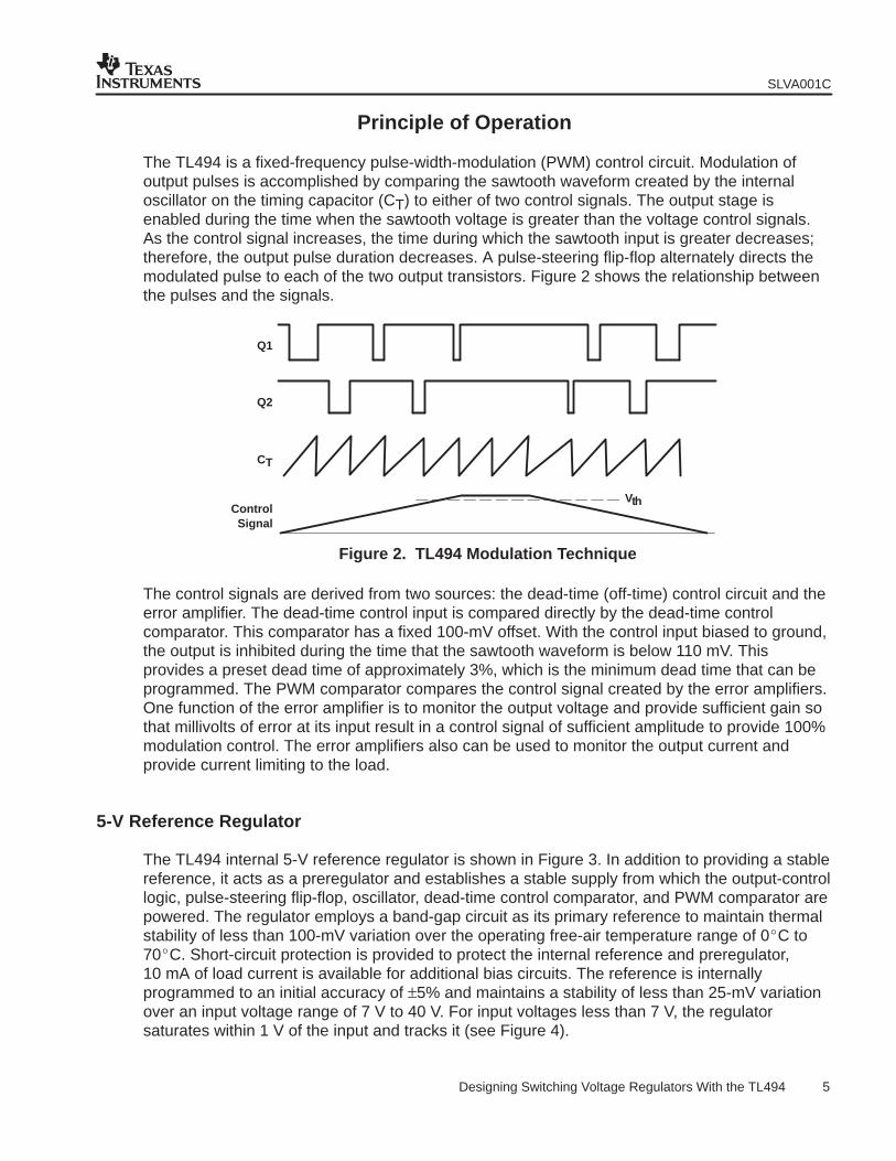
The TL494 is a fixed-frequency pulse-width-modulation (PWM) control circuit. Modulation ofoutput pulses is accomplished by comparing the sawtooth waveform created by the internaloscillator on the timing capacitor (CT) to either of two control signals. The output stage isenabled during the time when the sawtooth voltage is greater than the voltage control signals.As the control signal increases, the time during which the sawtooth input is greater decreases;therefore, the output pulse duration decreases. A pulse-steering flip-flop alternately directs themodulated pulse to each of the two output transistors. Figure 2 shows the relationship betweenthe pulses and the signals.
CT
ControlSignal
Vth
Q2
Q1
Figure 2. TL494 Modulation Technique
The control signals are derived from two sources: the dead-time (off-time) control circuit and theerror amplifier. The dead-time control input is compared directly by the dead-time controlcomparator. This comparator has a fixed 100-mV offset. With the control input biased to ground,the output is inhibited during the time that the sawtooth waveform is below 110 mV. Thisprovides a preset dead time of approximately 3%, which is the minimum dead time that can beprogrammed. The PWM comparator compares the control signal created by the error amplifiers.One function of the error amplifier is to monitor the output voltage and provide sufficient gain sothat millivolts of error at its input result in a control signal of sufficient amplitude to provide 100%modulation control. The error amplifiers also can be used to monitor the output current andprovide current limiting to the load.
5-V Reference Regulator
The TL494 internal 5-V reference regulator is shown in Figure 3. In addition to providing a stablereference, it acts as a preregulator and establishes a stable supply from which the output-controllogic, pulse-steering flip-flop, oscillator, dead-time control comparator, and PWM comparator arepowered. The regulator employs a band-gap circuit as its primary reference to maintain thermalstability of less than 100-mV variation over the operating free-air temperature range of 0C to70C. Short-circuit protection is provided to protect the internal reference and preregulator,10 mA of load current is available for additional bias circuits. The reference is internallyprogrammed to an initial accuracy of ±5% and maintains a stability of less than 25-mV variationover an input voltage range of 7 V to 40 V. For input voltages less than 7 V, the regulatorsaturates within 1 V of the input and tracks it (see Figure 4).

SLVA001C
6 Designing Switching Voltage Regulators With the TL494
VI
VREF(5 V)
Figure 3. 5-V Reference Regulator
5
4
3
2
1
00 1 2 3 4 5 6 7 40
VI − Input Voltage − V
6
VR
EF
− R
efer
ence
Vol
tage
− V
Figure 4. Reference Voltage vs Input Voltage
SLVA001C
7 Designing Switching Voltage Regulators With the TL494
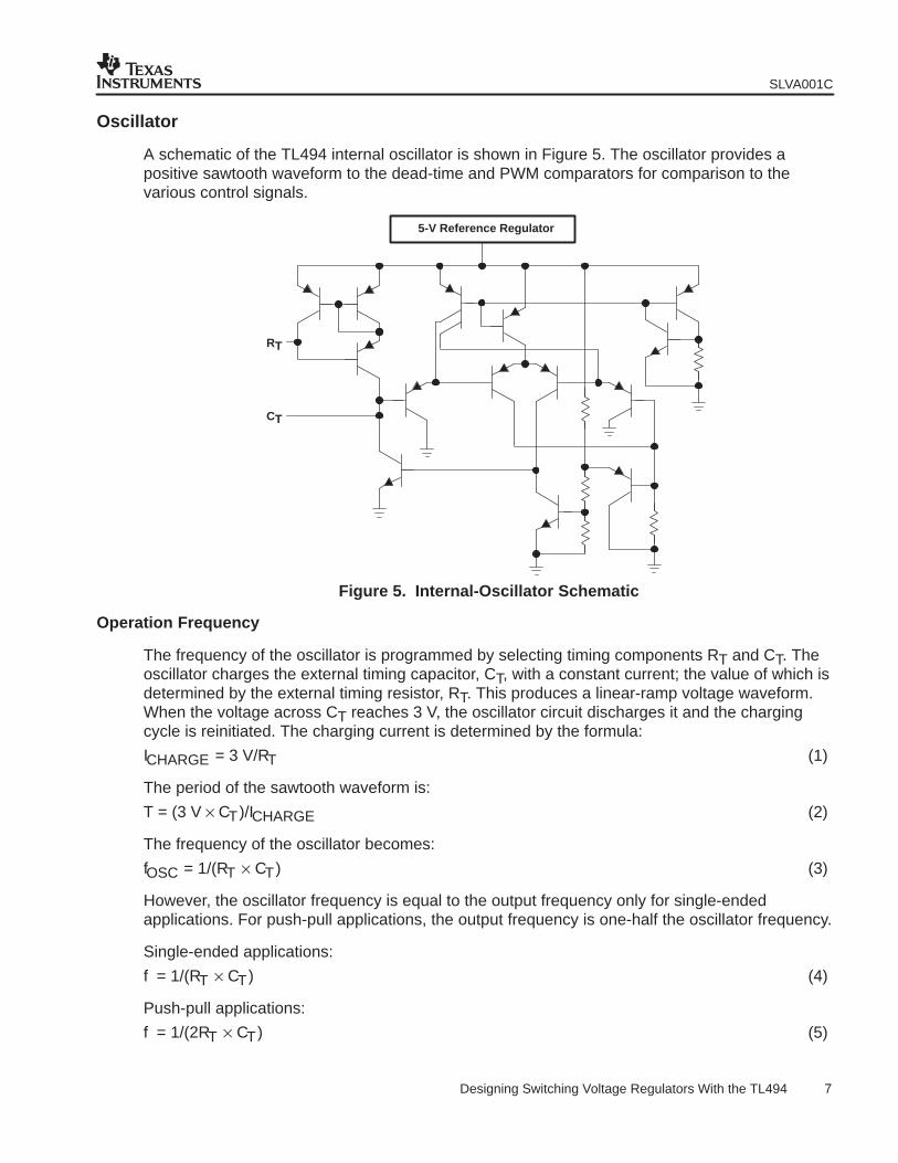
Oscillator
A schematic of the TL494 internal oscillator is shown in Figure 5. The oscillator provides apositive sawtooth waveform to the dead-time and PWM comparators for comparison to thevarious control signals.
CT
5-V Reference Regulator
RT
Figure 5. Internal-Oscillator Schematic
Operation Frequency
The frequency of the oscillator is programmed by selecting timing components RT and CT. Theoscillator charges the external timing capacitor, CT, with a constant current; the value of which isdetermined by the external timing resistor, RT. This produces a linear-ramp voltage waveform.When the voltage across CT reaches 3 V, the oscillator circuit discharges it and the chargingcycle is reinitiated. The charging current is determined by the formula:
ICHARGE = 3 V/RT
The period of the sawtooth waveform is:
T = (3 V × CT)/ICHARGE
The frequency of the oscillator becomes:
fOSC = 1/(RT × CT)
However, the oscillator frequency is equal to the output frequency only for single-endedapplications. For push-pull applications, the output frequency is one-half the oscillator frequency.
Single-ended applications:
f = 1/(RT × CT)
Push-pull applications:
f = 1/(2RT × CT)
(1)
(2)
(3)
(4)
(5)

SLVA001C
8 Designing Switching Voltage Regulators With the TL494
The oscillator is programmable over a range of 1 kHz to 300 kHz. Practical values for RT and CTrange from 1 kΩ to 500 kΩ and 470 pF to 10 µF, respectively. A plot of the oscillator frequencyversus RT and CT is shown in Figure 6. The stability of the oscillator for free-air temperaturesfrom 0C to 70C for various ranges of RT and CT also is shown in Figure 6.
1 M
100 k
10 k
1 k10 100 1 k 10 k 100 k 1 M
f − Frequency − Hz
1 µF
0.1 µF
0.01 µF0.001 µF
−1%
1%
−2%
−3%
−4%
NOTE: The percent of oscillator frequency variation over the 0°C to 70°C free-air temperature range is represented by dashed lines.
0
RT
− T
imin
g R
esis
tanc
e −
Figure 6. Oscillator Frequency vs R T/CT
Operation Above 150 kHz
At an operation frequency of 150 kHz, the period of the oscillator is 6.67 µs. The dead timeestablished by the internal offset of the dead-time comparator (~3% period) yields a blankingpulse of 200 ns. This is the minimum blanking pulse acceptable to ensure proper switching ofthe pulse-steering flip-flop. For frequencies above 150 kHz, additional dead time (above 3%) isprovided internally to ensure proper triggering and blanking of the internal pulse-steeringflip-flop. Figure 7 shows the relationship of internal dead time (expressed in percent) for variousvalues of RT and CT.
1 M
100 k
10 k
1 k10 100 1 k 10 k 100 k 1 M
f − Frequency − Hz
1 µF
0.1 µF
0.01 µF
0.001 µF
3%
4%
5%
6%RT
− T
imin
g R
esis
tanc
e −
Figure 7. Variation of Dead Time vs R T/CT
SLVA001C
9 Designing Switching Voltage Regulators With the TL494
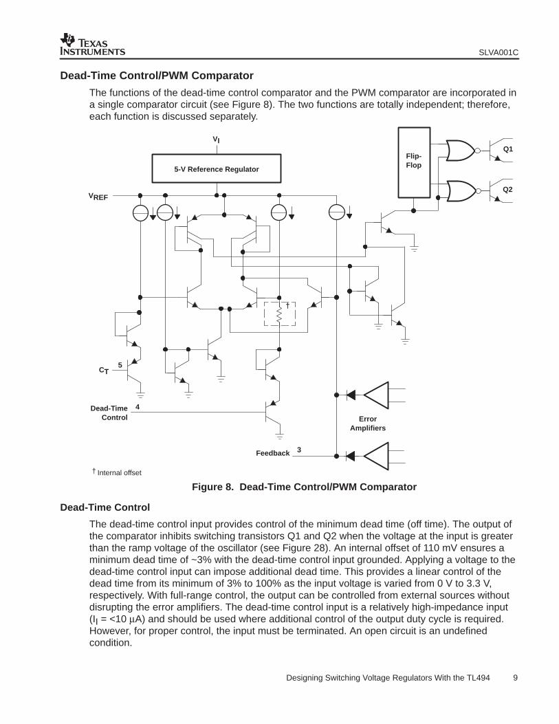
Dead-Time Control/PWM Comparator
The functions of the dead-time control comparator and the PWM comparator are incorporated ina single comparator circuit (see Figure 8). The two functions are totally independent; therefore,each function is discussed separately.
VREF
ErrorAmplifiers
Dead-TimeControl
CT
Feedback
5
4
3
5-V Reference Regulator
Flip-Flop
Q2
Q1
† Internal offset
†
VI
Figure 8. Dead-Time Control/PWM Comparator
Dead-Time Control
The dead-time control input provides control of the minimum dead time (off time). The output ofthe comparator inhibits switching transistors Q1 and Q2 when the voltage at the input is greaterthan the ramp voltage of the oscillator (see Figure 28). An internal offset of 110 mV ensures aminimum dead time of ~3% with the dead-time control input grounded. Applying a voltage to thedead-time control input can impose additional dead time. This provides a linear control of thedead time from its minimum of 3% to 100% as the input voltage is varied from 0 V to 3.3 V,respectively. With full-range control, the output can be controlled from external sources withoutdisrupting the error amplifiers. The dead-time control input is a relatively high-impedance input(II = <10 µA) and should be used where additional control of the output duty cycle is required.However, for proper control, the input must be terminated. An open circuit is an undefinedcondition.
SLVA001C
10 Designing Switching Voltage Regulators With the TL494
Comparator
The comparator is biased from the 5-V reference regulator. This provides isolation from the inputsupply for improved stability. The input of the comparator does not exhibit hysteresis, soprotection against false triggering near the threshold must be provided. The comparator has aresponse time of 400 ns from either of the control-signal inputs to the output transistors, withonly 100-mV of overdrive. This ensures positive control of the output within one-half cycle foroperation within the recommended 300-kHz range.
Pulse-Width Modulation (PWM)
The comparator also provides modulation control of the output pulse width. For this, the rampvoltage across timing capacitor CT is compared to the control signal present at the output of theerror amplifiers. The timing capacitor input incorporates a series diode that is omitted from thecontrol signal input. This requires the control signal (error amplifier output) to be ~0.7 V greaterthan the voltage across CT to inhibit the output logic, and ensures maximum duty cycleoperation without requiring the control voltage to sink to a true ground potential. The outputpulse width varies from 97% of the period to 0 as the voltage present at the error amplifier outputvaries from 0.5 V to 3.5 V, respectively.
Error Amplifiers
A schematic of the error amplifier circuit is shown in Figure 9. Both high-gain error amplifiersreceive their bias from the VI supply rail. This permits a common-mode input voltage range from–0.3 V to 2 V less than VI. Both amplifiers behave characteristically of a single-endedsingle-supply amplifier, in that each output is active high only. This allows each amplifier to pullup independently for a decreasing output pulse-width demand. With both outputs ORed togetherat the inverting input node of the PWM comparator, the amplifier demanding the minimum pulseout dominates. The amplifier outputs are biased low by a current sink to provide maximum pulsewidth out when both amplifiers are biased off.

SLVA001C
11 Designing Switching Voltage Regulators With the TL494
300 µA
CT
Feedback
PWMComparator
5-V ReferenceRegulator
VREF
AMP2
VI
InvertingInput
NoninvertingInput
+
−
Figure 9. Error Amplifiers
Figure 10 shows the output structure of the amplifiers operating into the 300-µA current sink.Attention must be given to this node for biasing considerations in gain-control andexternal-control interface circuits. Because the amplifier output is biased low only through acurrent sink (ISINK = 0.3 mA), bias current required by external circuitry into the feedbackterminal must not exceed the capability of the current sink. Otherwise, the maximum outputpulse width is limited. Figure 11 shows the proper biasing techniques for feedback gain control.
PWMComparator
300 µA
CT
ReferenceRegulator
VI
ErrorAmplifier 2
Feedback
ErrorAmplifier 1
Figure 10. Multiplex Structure of Error Amplifiers
SLVA001C
12 Designing Switching Voltage Regulators With the TL494
R1
_
+
_
+
To Output
13
2
13
2
To Output
VREF
R2
R1
RI
RF
VREF
RF
R2
RI
Figure 11. Error-Amplifier-Bias Configurations for Controlled-Gain Applications
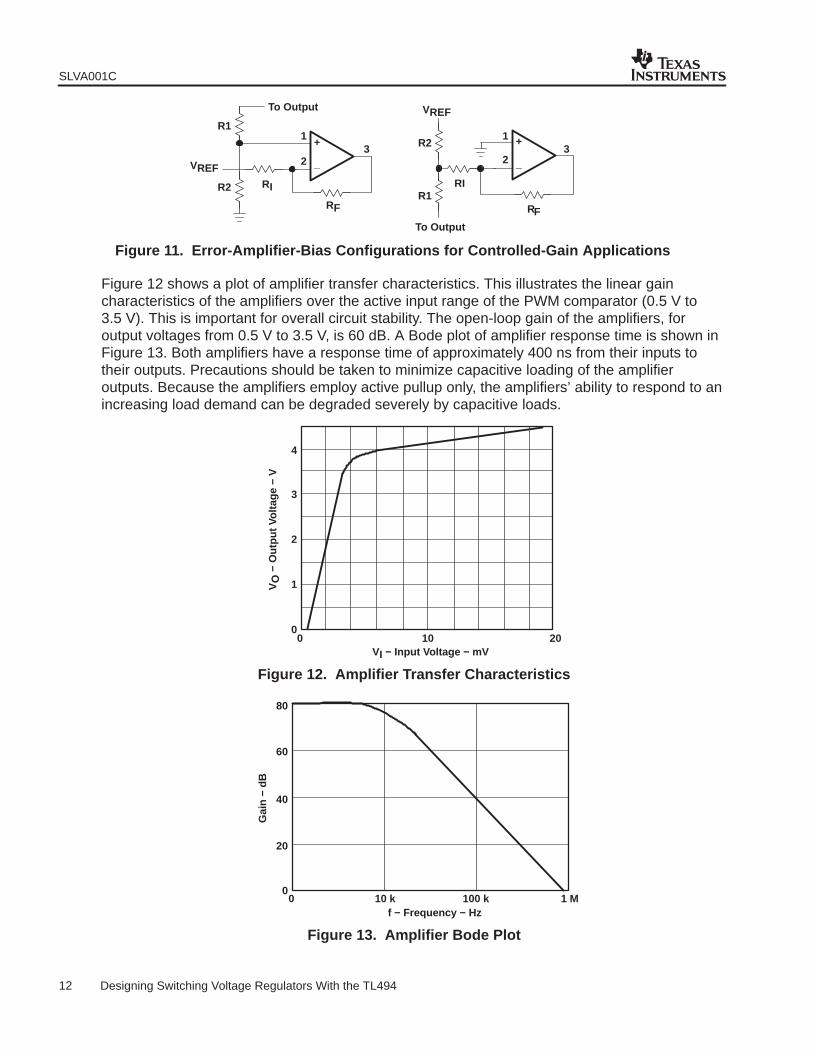
Figure 12 shows a plot of amplifier transfer characteristics. This illustrates the linear gaincharacteristics of the amplifiers over the active input range of the PWM comparator (0.5 V to3.5 V). This is important for overall circuit stability. The open-loop gain of the amplifiers, foroutput voltages from 0.5 V to 3.5 V, is 60 dB. A Bode plot of amplifier response time is shown inFigure 13. Both amplifiers have a response time of approximately 400 ns from their inputs totheir outputs. Precautions should be taken to minimize capacitive loading of the amplifieroutputs. Because the amplifiers employ active pullup only, the amplifiers’ ability to respond to anincreasing load demand can be degraded severely by capacitive loads.
4
3
2
1
00 10 20
VI − Input Voltage − mV
VO
− O
utpu
t Vol
tage
− V
Figure 12. Amplifier Transfer Characteristics
80
60
40
20
00 10 k 1 M
f − Frequency − Hz100 k
Gai
n −
dB
Figure 13. Amplifier Bode Plot
SLVA001C
13 Designing Switching Voltage Regulators With the TL494
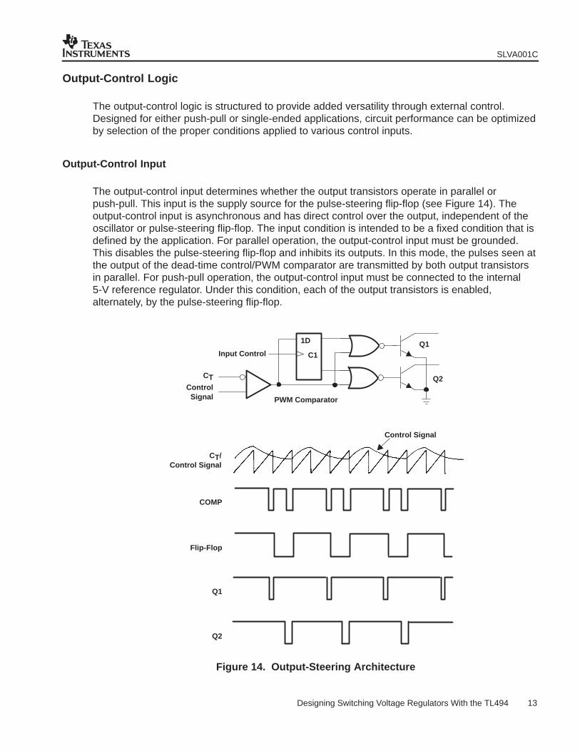
Output-Control Logic
The output-control logic is structured to provide added versatility through external control.Designed for either push-pull or single-ended applications, circuit performance can be optimizedby selection of the proper conditions applied to various control inputs.
Output-Control Input
The output-control input determines whether the output transistors operate in parallel orpush-pull. This input is the supply source for the pulse-steering flip-flop (see Figure 14). Theoutput-control input is asynchronous and has direct control over the output, independent of theoscillator or pulse-steering flip-flop. The input condition is intended to be a fixed condition that isdefined by the application. For parallel operation, the output-control input must be grounded.This disables the pulse-steering flip-flop and inhibits its outputs. In this mode, the pulses seen atthe output of the dead-time control/PWM comparator are transmitted by both output transistorsin parallel. For push-pull operation, the output-control input must be connected to the internal5-V reference regulator. Under this condition, each of the output transistors is enabled,alternately, by the pulse-steering flip-flop.
CTControl
Signal
Input Control C1
1D Q1
Q2
PWM Comparator
COMP
Flip-Flop
Q1
Q2
Control Signal
CT/Control Signal
Figure 14. Output-Steering Architecture
SLVA001C
14 Designing Switching Voltage Regulators With the TL494
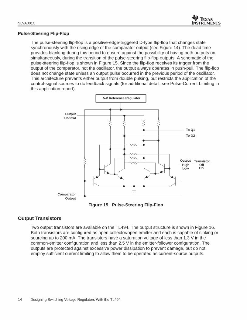
Pulse-Steering Flip-Flop
The pulse-steering flip-flop is a positive-edge-triggered D-type flip-flop that changes statesynchronously with the rising edge of the comparator output (see Figure 14). The dead timeprovides blanking during this period to ensure against the possibility of having both outputs on,simultaneously, during the transition of the pulse-steering flip-flop outputs. A schematic of thepulse-steering flip-flop is shown in Figure 15. Since the flip-flop receives its trigger from theoutput of the comparator, not the oscillator, the output always operates in push-pull. The flip-flopdoes not change state unless an output pulse occurred in the previous period of the oscillator.This architecture prevents either output from double pulsing, but restricts the application of thecontrol-signal sources to dc feedback signals (for additional detail, see Pulse-Current Limiting inthis application report).
OutputControl
To Q1
To Q2
5-V Reference Regulator
ComparatorOutput
OutputHighLow
TransistorOffOn
Figure 15. Pulse-Steering Flip-Flop
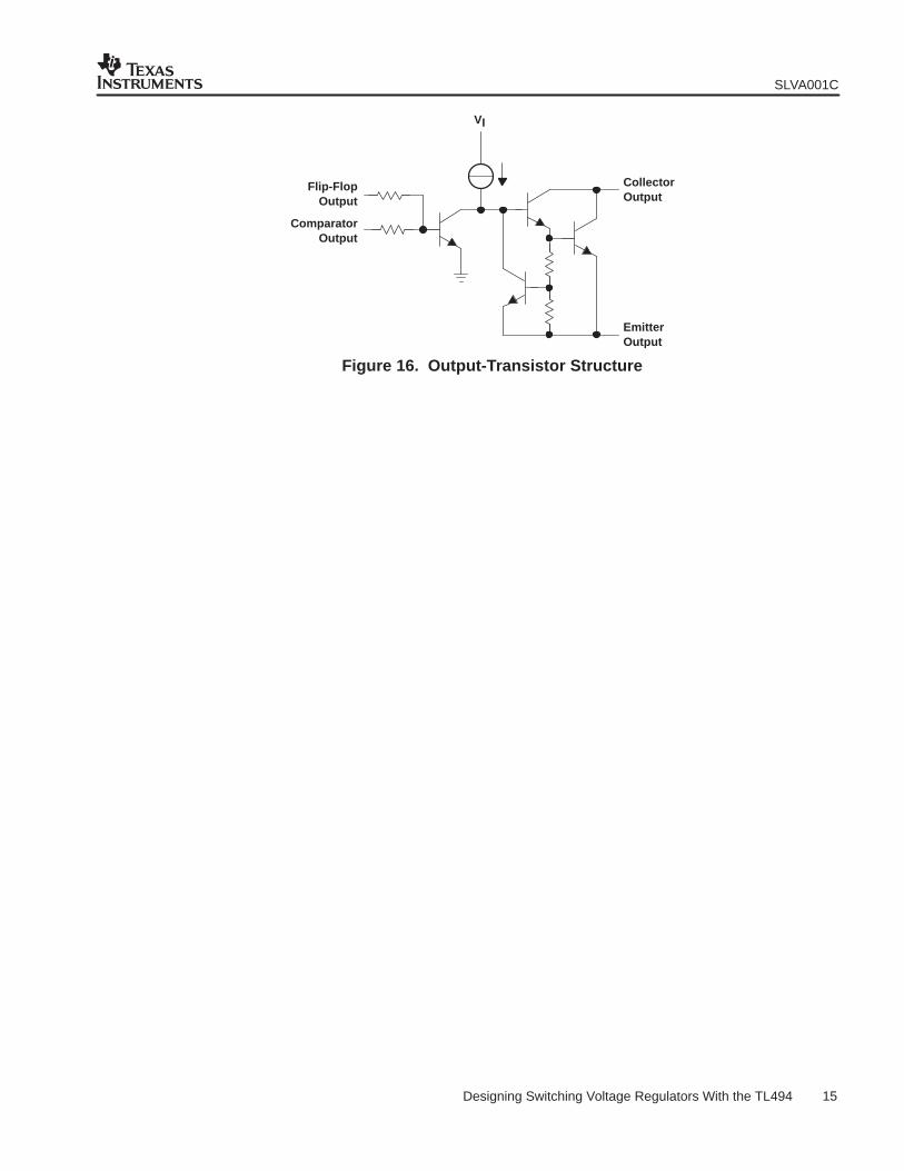
Output Transistors
Two output transistors are available on the TL494. The output structure is shown in Figure 16.Both transistors are configured as open collector/open emitter and each is capable of sinking orsourcing up to 200 mA. The transistors have a saturation voltage of less than 1.3 V in thecommon-emitter configuration and less than 2.5 V in the emitter-follower configuration. Theoutputs are protected against excessive power dissipation to prevent damage, but do notemploy sufficient current limiting to allow them to be operated as current-source outputs.
SLVA001C
15 Designing Switching Voltage Regulators With the TL494
VI
Flip-FlopOutput
CollectorOutput
ComparatorOutput
EmitterOutput
Figure 16. Output-Transistor Structure
SLVA001C
16 Designing Switching Voltage Regulators With the TL494
Applications
Reference Regulator
The internal 5-V reference regulator is designed primarily to provide the internal circuitry with astable supply rail for varying input voltages. The regulator provides sufficient drive to sustain upto 10 mA of supply current to additional load circuitry. However, excessive loading may degradethe performance of the TL494 because the 5-V reference regulator establishes the supplyvoltage of much of the internal control circuitry.
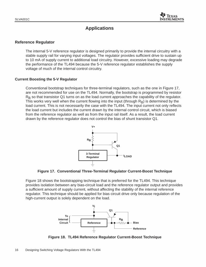
Current Boosting the 5-V Regulator
Conventional bootstrap techniques for three-terminal regulators, such as the one in Figure 17,are not recommended for use on the TL494. Normally, the bootstrap is programmed by resistorRB so that transistor Q1 turns on as the load current approaches the capability of the regulator.This works very well when the current flowing into the input (through RB) is determined by theload current. This is not necessarily the case with the TL494. The input current not only reflectsthe load current but includes the current drawn by the internal control circuit, which is biasedfrom the reference regulator as well as from the input rail itself. As a result, the load currentdrawn by the reference regulator does not control the bias of shunt transistor Q1.
RB
3-TerminalRegulator
V+
Q1
ILOAD
Figure 17. Conventional Three-Terminal Regulator Current-Boost Technique
Figure 18 shows the bootstrapping technique that is preferred for the TL494. This techniqueprovides isolation between any bias-circuit load and the reference regulator output and providesa sufficient amount of supply current, without affecting the stability of the internal referenceregulator. This technique should be applied for bias circuit drive only because regulation of thehigh-current output is solely dependent on the load.
Reference
VIQ1
ToInternalCircuit
Reference
BiasRB
Figure 18. TL494 Reference Regulator Current-Boost Technique
SLVA001C
17 Designing Switching Voltage Regulators With the TL494
Applications of the Oscillator
The design of the internal oscillator allows a great deal of flexibility in the operation of the TL494control circuit.
Synchronization
Synchronizing two or more oscillators in a common system easily is accomplished with thearchitecture of the TL494 control circuits. Since the internal oscillator is used only for creation ofthe sawtooth waveform on the timing capacitor, the oscillator can be inhibited as long as acompatible sawtooth waveform is provided externally to the timing capacitor terminal.Terminating the RT terminal to the reference-supply output can inhibit the internal oscillator.
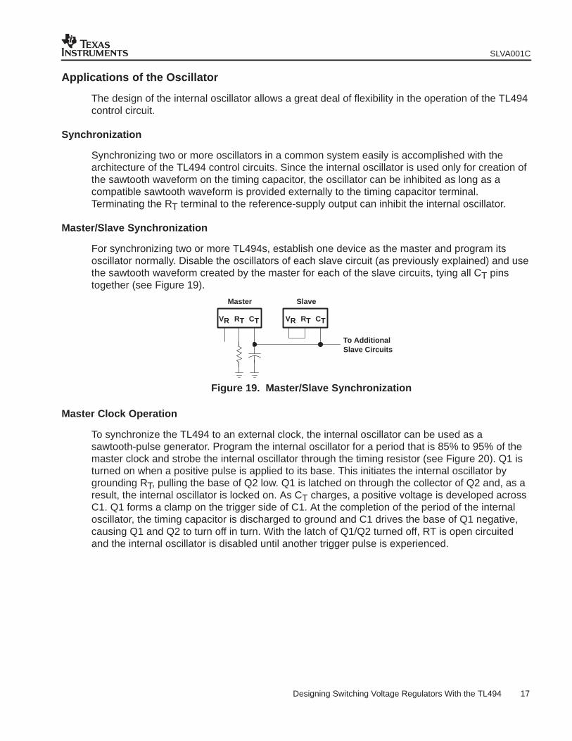
Master/Slave Synchronization
For synchronizing two or more TL494s, establish one device as the master and program itsoscillator normally. Disable the oscillators of each slave circuit (as previously explained) and usethe sawtooth waveform created by the master for each of the slave circuits, tying all CT pinstogether (see Figure 19).
VR RT CT VR RT CT
Master Slave
To AdditionalSlave Circuits
Figure 19. Master/Slave Synchronization
Master Clock Operation
To synchronize the TL494 to an external clock, the internal oscillator can be used as asawtooth-pulse generator. Program the internal oscillator for a period that is 85% to 95% of themaster clock and strobe the internal oscillator through the timing resistor (see Figure 20). Q1 isturned on when a positive pulse is applied to its base. This initiates the internal oscillator bygrounding RT, pulling the base of Q2 low. Q1 is latched on through the collector of Q2 and, as aresult, the internal oscillator is locked on. As CT charges, a positive voltage is developed acrossC1. Q1 forms a clamp on the trigger side of C1. At the completion of the period of the internaloscillator, the timing capacitor is discharged to ground and C1 drives the base of Q1 negative,causing Q1 and Q2 to turn off in turn. With the latch of Q1/Q2 turned off, RT is open circuitedand the internal oscillator is disabled until another trigger pulse is experienced.

SLVA001C
18 Designing Switching Voltage Regulators With the TL494
VREF
D1
RTQ2
RT
CTC1
Q1
CT
Figure 20. External Clock Synchronization
A common problem occurs during start-up when synchronizing the power supply to a systemclock. Normally, an additional start-up oscillator is required. Again, the internal oscillator can beused by modifying the previous circuit slightly (see Figure 21). During power up, when the outputvoltage is low, Q3 is biased on, causing Q1 to stay on and the internal oscillator to behavenormally. Once the output voltage has increased sufficiently (VO > VREF for Figure 21), Q3 nolonger is biased on and the Q1/Q2 latch becomes dependent on the trigger signal, as previouslydiscussed.
VREF
D1
RT
Q2
RT
CTC1
Q1
CT
Q3
VO
Figure 21. Oscillator Start-Up Circuit
Fail-Safe Operation
With the modulation scheme employed by the TL494 and the structure of the oscillator, theTL494 inherently turns off if either timing component fails. If timing resistor RT opens, no currentis provided by the oscillator to charge CT. The addition of a bleeder resistor (see Figure 22)ensures the discharge of CT. With the CT input at ground, or if CT short circuits, both outputs areinhibited.
RT
CT
CT(1/10) RT
RT
Figure 22. Fail-Safe Protection

SLVA001C
19 Designing Switching Voltage Regulators With the TL494
Error-Amplifier-Bias Configuration
The design of the TL494 employs both amplifiers in a noninverting configuration. Figure 23shows the proper bias circuits for negative and positive output voltages. The gain controlcircuits, shown in Figure 11, can be integrated into the bias circuits.
_+
_+
VO VREF R1R2
Output
VREF
VO VREF1 R1
R2
Output
R1
R2
VREF
R1
R2
Positive Output Configuration Negative Output Configuration
Figure 23. Error-Amplifier-Bias Configurations
Current Limiting
Either amplifier provided on the TL494 can be used for fold-back current limiting. Application ofeither amplifier is limited primarily to load-current control. The architecture defines that theseamplifiers be used for dc control applications. Both amplifiers have a broad common-modevoltage range that allows direct current sensing at the output voltage rails. Several techniquescan be employed for current limiting.
Fold-Back Current Limiting
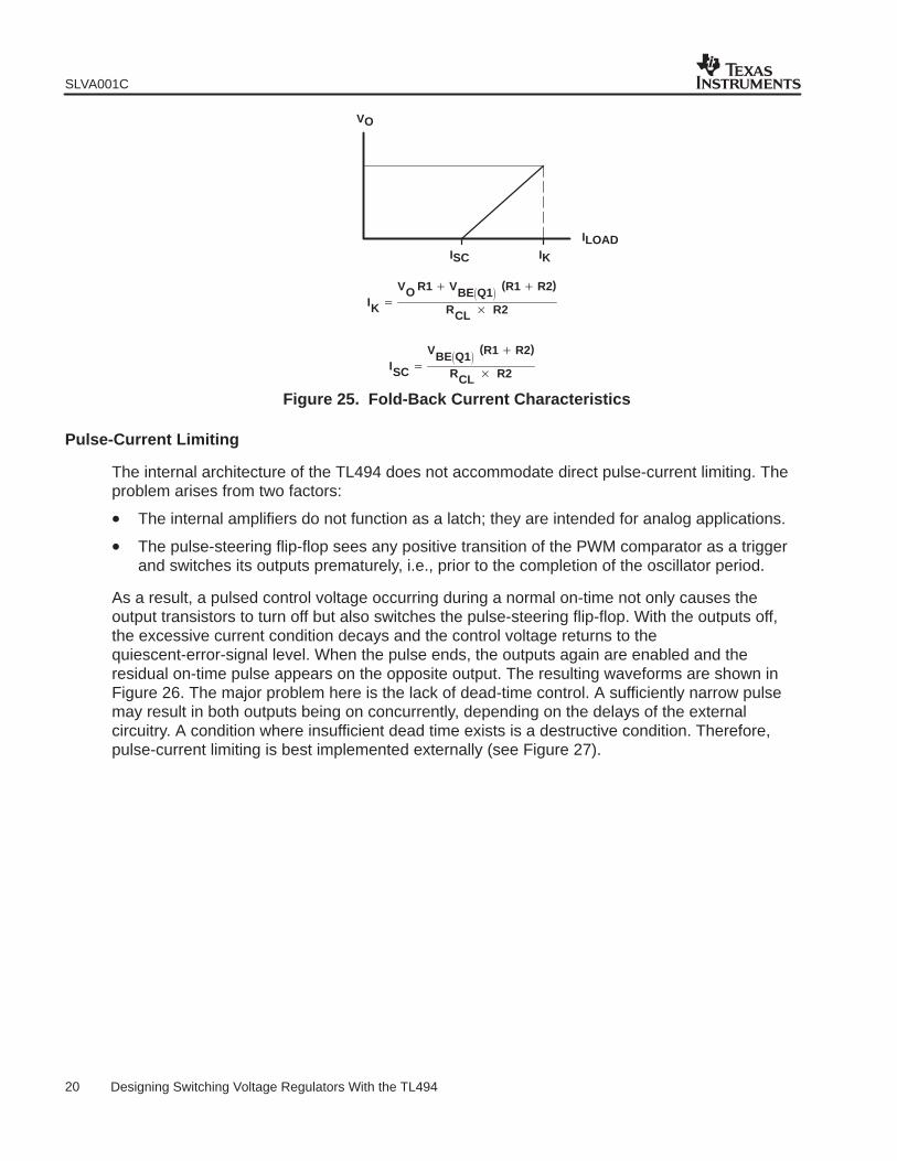
Figure 24 shows a circuit that employs the proper bias technique for fold-back current limiting.Initial current limiting occurs when sufficient voltage is developed across RCL to compensate forthe base-emitter voltage of Q1, plus the voltage across R1. When current limiting occurs, theoutput voltage drops. As the output decays, the voltage across R1 decreases proportionally.This results in less voltage required across RCL to maintain current limiting. The resulting outputcharacteristics are shown in Figure 25.
_+
RCLCF
R1
R2
Q1
Figure 24. Fold-Back Current Limiting
SLVA001C
20 Designing Switching Voltage Regulators With the TL494
ILOAD
VO
ISC IK
IK VO R1 VBEQ1
(R1 R2)
RCL R2
ISC VBEQ1
(R1 R2)
RCL R2
Figure 25. Fold-Back Current Characteristics
Pulse-Current Limiting
The internal architecture of the TL494 does not accommodate direct pulse-current limiting. Theproblem arises from two factors:
• The internal amplifiers do not function as a latch; they are intended for analog applications.
• The pulse-steering flip-flop sees any positive transition of the PWM comparator as a triggerand switches its outputs prematurely, i.e., prior to the completion of the oscillator period.
As a result, a pulsed control voltage occurring during a normal on-time not only causes theoutput transistors to turn off but also switches the pulse-steering flip-flop. With the outputs off,the excessive current condition decays and the control voltage returns to thequiescent-error-signal level. When the pulse ends, the outputs again are enabled and theresidual on-time pulse appears on the opposite output. The resulting waveforms are shown inFigure 26. The major problem here is the lack of dead-time control. A sufficiently narrow pulsemay result in both outputs being on concurrently, depending on the delays of the externalcircuitry. A condition where insufficient dead time exists is a destructive condition. Therefore,pulse-current limiting is best implemented externally (see Figure 27).

SLVA001C
21 Designing Switching Voltage Regulators With the TL494
OutputControlLogic
Flip-FlopDead-Time
Control
Q2
Q1
Error Signal
Pulse Signal ResponseQ1
Q2
Control Signal
Control Signal/C T
Q1
Q2
Expected Outputs
Actual Outputs
Figure 26. Error-Signal Considerations
VREF
D1
CT
SwitchingCircuit
Dead-TimeControl
Q2
Q3 Q1
50 kΩ
1 MΩ
RCL
Figure 27. Peak-Current Protection
In Figure 27, the current in the switching transistors is sensed by RCL. When there is sufficientcurrent, the sensing transistor Q1 is forward biased, the base of Q2 is pulled low through Q1,and the dead-time control input is pulled to the 5-V reference. Drive for the base of Q3 isprovided through the collector of Q2. Q3 acts as a latch to maintain Q2 in a saturated state whenQ1 turns off, as the current decays through RCL. The latch remains in this state, inhibiting theoutput transistors, until the oscillator completes its period and discharges CT to 0 V. When thisoccurs, the Schottky diode (D1) forward biases and turns off Q3 and Q2, allowing the dead-timecontrol to return to its programmed voltage.

SLVA001C
22 Designing Switching Voltage Regulators With the TL494
Applications of the Dead-Time Control
The primary function of the dead-time control is to control the minimum off time of the output ofthe TL494. The dead-time control input provides control from 5% to 100% dead time (seeFigure 28).
OutputControlLogic
Dead-TimeControl
Output
Osc
5% Dead Time
Control Input
CT
Figure 28. Dead-Time Control Characteristics
Therefore, the TL494 can be tailored to the specific power transistor switches that are used toensure that the output transistors never experience a common on time. The bias circuit for thebasic function is shown in Figure 29. The dead-time control can be used for many other controlsignals.
VREF
R2
R1
Dead-Time ControlIn
TD = RT CT (0.05 + 0.35 R2)R2 in k ΩR1 + R2 = 5 kΩ
Figure 29. Tailored Dead Time
Soft Start
With the availability of the dead-time control, input implementation of a soft-start circuit isrelatively simple; Figure 30 shows one example. Initially, capacitor CS forces the dead-timecontrol input to follow the 5-V reference regulator that disables both outputs, i.e., 100% deadtime. As the capacitor charges through RS, the output pulse slowly increases until the controlloop takes command. If additional control is to be introduced at this input, a blocking diodeshould be used to isolate the soft-start circuit. If soft start is desired in conjunction with a tailoreddead time, the circuit in Figure 29 can be used with the addition of capacitor CS across R1.
SLVA001C
23 Designing Switching Voltage Regulators With the TL494
RS R2
VREF
Dead-Time Control
CS R1
Figure 30. Soft-Start Circuit
The use of a blocking diode for soft-start protection is recommended. Not only does suchcircuitry prevent large current surges during power up, it also protects against any false signalsthat might be created by the control circuit as power is applied.
Overvoltage Protection
The dead-time control also provides a convenient input for overvoltage protection that may besensed as an output voltage condition or input protection. Figure 31 shows a TL431 as thesensing element. When the supply rail being monitored increases to the point that 2.5 V isdeveloped at the driver node of R1 and R2, the TL431 goes into conduction. This forward biasesQ1, causing the dead-time control to be pulled up to the reference voltage and disabling theoutput transistors.
VREF
Dead-TimeControl
R1Q1
R2
MonitoredSupply Rail
TL431
Figure 31. Overvoltage-Protection Circuit
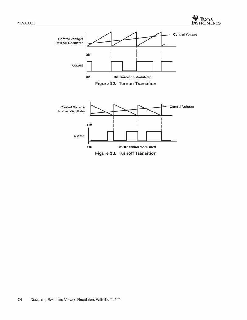
Modulation of Turnon/Turnoff Transition
Modulation of the output pulse by the TL494 is accomplished by modulating the turnon transitionof the output transistors. The turnoff transition always is concurrent with the falling edge of theoscillator waveform. Figure 32 shows the oscillator output as it is compared to a varying controlsignal and the resulting output waveforms. If modulation of the turnoff transition is desired, anexternal negative slope sawtooth waveform (see Figure 33) can be used without degrading theoverall performance of the TL494.
SLVA001C
24 Designing Switching Voltage Regulators With the TL494
Control VoltageControl Voltage/
Internal Oscillator
Output
Off
On On-Transition Modulated
Figure 32. Turnon Transition
Control VoltageControl Voltage/Internal Oscillator
Output
Off
On Off-Transition Modulated
Figure 33. Turnoff Transition

SLVA001C
25 Designing Switching Voltage Regulators With the TL494
Design Example
The following design example uses the TL494 to create a 5-V/10-A power supply. This design isbased on the following parameters:
VO = 5 VVI = 32 VIO = 10 AfOSC = 20-kHz switching frequencyVR = 20-mV peak-to-peak (VRIPPLE)∆IL = 1.5-A inductor current change
Input Power Source
The 32-V dc power source for this supply uses a 120-V input, 24-V output transformer rated at75 VA. The 24-V secondary winding feeds a full-wave bridge rectifier followed by acurrent-limiting resistor (0.3 Ω) and two filter capacitors (see Figure 34).
20,000 F
BridgeRectifiers3 A/50 V
20,000 F0.3 Ω
120 V24 V3 A
+32 V
−
+ +
Figure 34. Input Power Source
The output current and voltage are determined by equations 6 and 7:
VRECTIFIER VSECONDARY 2 24 V 2 34 V
IRECTIFIER(AVG) (VOVI ) IO 5 V32 V 10 A 1.6 A
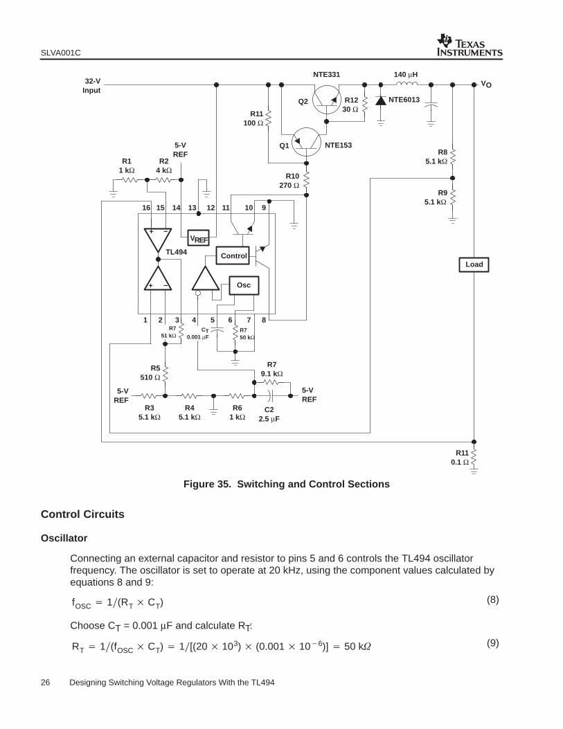
The 3-A/50-V full-wave bridge rectifier meets these calculated conditions. Figure 35 shows theswitching and control sections.
(6)
(7)
SLVA001C
26 Designing Switching Voltage Regulators With the TL494
VREF
R11 kΩ
LoadControl
Osc
NTE331 140 µHVO
NTE6013
NTE153
TL494
R24 kΩ
5-VREF
R11100 Ω
R1230 Ω
R10270 Ω
1 2 3 4 6 7 8
910111213141516
R751 kΩ
R750 kΩ
R5510 Ω
R79.1 kΩ
R35.1 kΩ
R45.1 kΩ
R61 kΩ
C22.5 µF
5-VREF
5-VREF
R110.1 Ω
CT0.001 µF
5
R85.1 k
R95.1 k
Q2
Q1
+ −
+ −
32-VInput
Figure 35. Switching and Control Sections
Control Circuits
Oscillator
Connecting an external capacitor and resistor to pins 5 and 6 controls the TL494 oscillatorfrequency. The oscillator is set to operate at 20 kHz, using the component values calculated byequations 8 and 9:
fOSC 1(RT CT)
Choose CT = 0.001 µF and calculate RT:
RT 1(fOSC CT) 1[(20 103) (0.001 106)] 50 k
(8)
(9)
SLVA001C
27 Designing Switching Voltage Regulators With the TL494
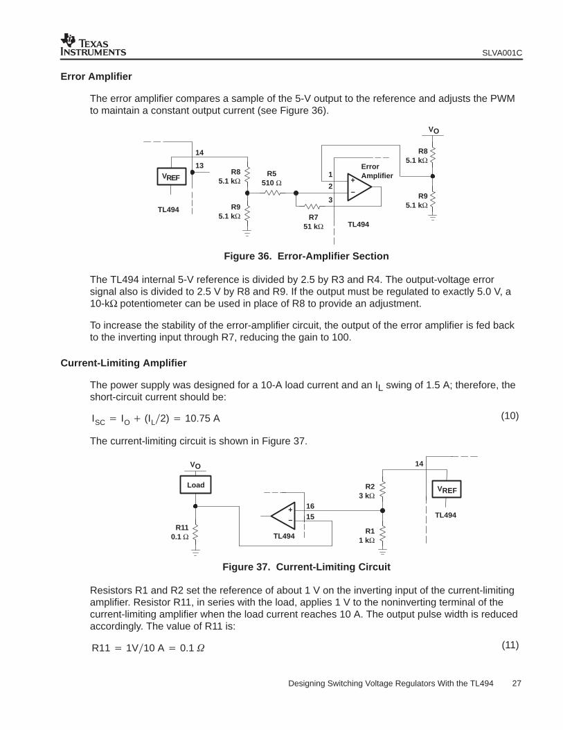
Error Amplifier
The error amplifier compares a sample of the 5-V output to the reference and adjusts the PWMto maintain a constant output current (see Figure 36).
R85.1 kΩ
VO
VREF +
−
1
14
13 ErrorAmplifier
2
3
TL494
R95.1 kΩ
R5510 Ω
R751 kΩ
R85.1 kΩ
R95.1 kΩ
TL494
Figure 36. Error-Amplifier Section
The TL494 internal 5-V reference is divided by 2.5 by R3 and R4. The output-voltage errorsignal also is divided to 2.5 V by R8 and R9. If the output must be regulated to exactly 5.0 V, a10-kΩ potentiometer can be used in place of R8 to provide an adjustment.
To increase the stability of the error-amplifier circuit, the output of the error amplifier is fed backto the inverting input through R7, reducing the gain to 100.
Current-Limiting Amplifier
The power supply was designed for a 10-A load current and an IL swing of 1.5 A; therefore, theshort-circuit current should be:
ISC IO (IL2) 10.75 A
The current-limiting circuit is shown in Figure 37.
R110.1 Ω
Load
VO
VREF
TL494
TL494+−
R23 kΩ
R11 kΩ
14
1615
Figure 37. Current-Limiting Circuit
Resistors R1 and R2 set the reference of about 1 V on the inverting input of the current-limitingamplifier. Resistor R11, in series with the load, applies 1 V to the noninverting terminal of thecurrent-limiting amplifier when the load current reaches 10 A. The output pulse width is reducedaccordingly. The value of R11 is:
R11 1V10 A 0.1
(10)
(11)

SLVA001C
28 Designing Switching Voltage Regulators With the TL494
Soft Start and Dead Time
To reduce stress on the switching transistors at start-up, the start-up surge that occurs as theoutput filter capacitor charges must be reduced. The availability of the dead-time control makesimplementation of a soft-start circuit relatively simple (see Figure 38).
TL494
Pin 4 Voltage
PWM Output
Oscillator Ramp Voltage
ton
RTC2
+5 V
0.1 V
Osc
R6
14
5
4
7
Oscillator Ramp
+
Figure 38. Soft-Start Circuit
The soft-start circuit allows the pulse width at the output to increase slowly (see Figure 38) byapplying a negative slope waveform to the dead-time control input (pin 4).
Initially, capacitor C2 forces the dead-time control input to follow the 5-V regulator, whichdisables the outputs (100% dead time). As the capacitor charges through R6, the output pulsewidth slowly increases until the control loop takes command. With a resistor ratio of 1:10 for R6and R7, the voltage at pin 4 after start-up is 0.1 × 5 V, or 0.5 V.
The soft-start time generally is in the range of 25 to 100 clock cycles. If 50 clock cycles at a20-kHz switching rate is selected, the soft-start time is:
t 1f 120 kHz 50 s per clock cycle
The value of the capacitor then is determined by:
C2 soft−start timeR6 (50 s 50 cycles)1 k 2.5 s
This helps eliminate any false signals that might be created by the control circuit as power isapplied.
(12)
(13)
SLVA001C
29 Designing Switching Voltage Regulators With the TL494
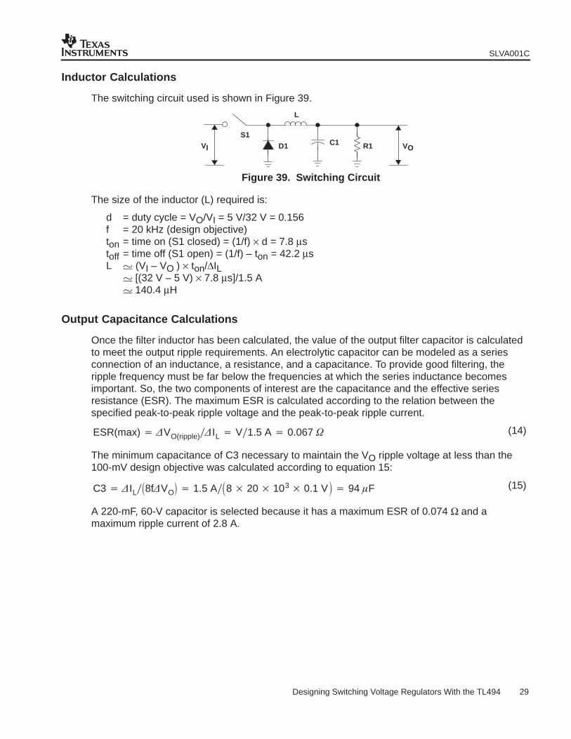
Inductor Calculations
The switching circuit used is shown in Figure 39.
R1C1D1
S1
L
VOVI
Figure 39. Switching Circuit
The size of the inductor (L) required is:
d = duty cycle = VO/VI = 5 V/32 V = 0.156f = 20 kHz (design objective)ton = time on (S1 closed) = (1/f) × d = 7.8 µstoff = time off (S1 open) = (1/f) – ton = 42.2 µsL (VI – VO ) × ton/∆IL [(32 V – 5 V) × 7.8 µs]/1.5 A 140.4 µH
Output Capacitance Calculations
Once the filter inductor has been calculated, the value of the output filter capacitor is calculatedto meet the output ripple requirements. An electrolytic capacitor can be modeled as a seriesconnection of an inductance, a resistance, and a capacitance. To provide good filtering, theripple frequency must be far below the frequencies at which the series inductance becomesimportant. So, the two components of interest are the capacitance and the effective seriesresistance (ESR). The maximum ESR is calculated according to the relation between thespecified peak-to-peak ripple voltage and the peak-to-peak ripple current.
ESR(max) VO(ripple)IL V1.5 A 0.067
The minimum capacitance of C3 necessary to maintain the VO ripple voltage at less than the100-mV design objective was calculated according to equation 15:
C3 IL8fVO 1.5 A8 20 103 0.1 V 94 F
A 220-mF, 60-V capacitor is selected because it has a maximum ESR of 0.074 Ω and amaximum ripple current of 2.8 A.
(14)
(15)
SLVA001C
30 Designing Switching Voltage Regulators With the TL494
Transistor Power-Switch Calculations
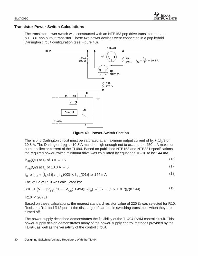
The transistor power switch was constructed with an NTE153 pnp drive transistor and anNTE331 npn output transistor. These two power devices were connected in a pnp hybridDarlington circuit configuration (see Figure 40).
NTE331
TL494
Control
Q2
11 10 9
Q1NTE153
32 V
8
R10270 Ω
R1230 Ω
R11100 Ω IO
IL2
10.8 A
Figure 40. Power-Switch Section
The hybrid Darlington circuit must be saturated at a maximum output current of IO + ∆IL/2 or10.8 A. The Darlington hFE at 10.8 A must be high enough not to exceed the 250-mA maximumoutput collector current of the TL494. Based on published NTE153 and NTE331 specifications,the required power-switch minimum drive was calculated by equations 16–18 to be 144 mA:
hFE(Q1) at IC of 3 A 15
hFE(Q2) at IC of 10.0 A 5
iB [IO IL2] [hFE(Q2) hFE(Q1)] 144 mA
The value of R10 was calculated by:
R10 VI [VBE(Q1) VCE(TL494)][iB] [32 (1.5 0.7)](0.144)
R10 207
Based on these calculations, the nearest standard resistor value of 220 Ω was selected for R10.Resistors R11 and R12 permit the discharge of carriers in switching transistors when they areturned off.
The power supply described demonstrates the flexibility of the TL494 PWM control circuit. Thispower-supply design demonstrates many of the power-supply control methods provided by theTL494, as well as the versatility of the control circuit.
(16)
(17)
(18)
(19)
IMPORTANT NOTICE
Texas Instruments Incorporated and its subsidiaries (TI) reserve the right to make corrections, modifications,enhancements, improvements, and other changes to its products and services at any time and to discontinueany product or service without notice. Customers should obtain the latest relevant information before placingorders and should verify that such information is current and complete. All products are sold subject to TI’s termsand conditions of sale supplied at the time of order acknowledgment.
TI warrants performance of its hardware products to the specifications applicable at the time of sale inaccordance with TI’s standard warranty. Testing and other quality control techniques are used to the extent TIdeems necessary to support this warranty. Except where mandated by government requirements, testing of allparameters of each product is not necessarily performed.
TI assumes no liability for applications assistance or customer product design. Customers are responsible fortheir products and applications using TI components. To minimize the risks associated with customer productsand applications, customers should provide adequate design and operating safeguards.
TI does not warrant or represent that any license, either express or implied, is granted under any TI patent right,copyright, mask work right, or other TI intellectual property right relating to any combination, machine, or processin which TI products or services are used. Information published by TI regarding third-party products or servicesdoes not constitute a license from TI to use such products or services or a warranty or endorsement thereof.Use of such information may require a license from a third party under the patents or other intellectual propertyof the third party, or a license from TI under the patents or other intellectual property of TI.
Reproduction of information in TI data books or data sheets is permissible only if reproduction is withoutalteration and is accompanied by all associated warranties, conditions, limitations, and notices. Reproductionof this information with alteration is an unfair and deceptive business practice. TI is not responsible or liable forsuch altered documentation.
Resale of TI products or services with statements different from or beyond the parameters stated by TI for thatproduct or service voids all express and any implied warranties for the associated TI product or service andis an unfair and deceptive business practice. TI is not responsible or liable for any such statements.
Following are URLs where you can obtain information on other Texas Instruments products and applicationsolutions:
Products Applications
Amplifiers amplifier.ti.com Audio www.ti.com/audio
Data Converters dataconverter.ti.com Automotive www.ti.com/automotive
DSP dsp.ti.com Broadband www.ti.com/broadband
Interface interface.ti.com Digital Control www.ti.com/digitalcontrol
Logic logic.ti.com Military www.ti.com/military
Power Mgmt power.ti.com Optical Networking www.ti.com/opticalnetwork
Microcontrollers microcontroller.ti.com Security www.ti.com/security
Telephony www.ti.com/telephony
Video & Imaging www.ti.com/video
Wireless www.ti.com/wireless
Mailing Address: Texas Instruments
Post Office Box 655303 Dallas, Texas 75265
Copyright 2004, Texas Instruments Incorporated