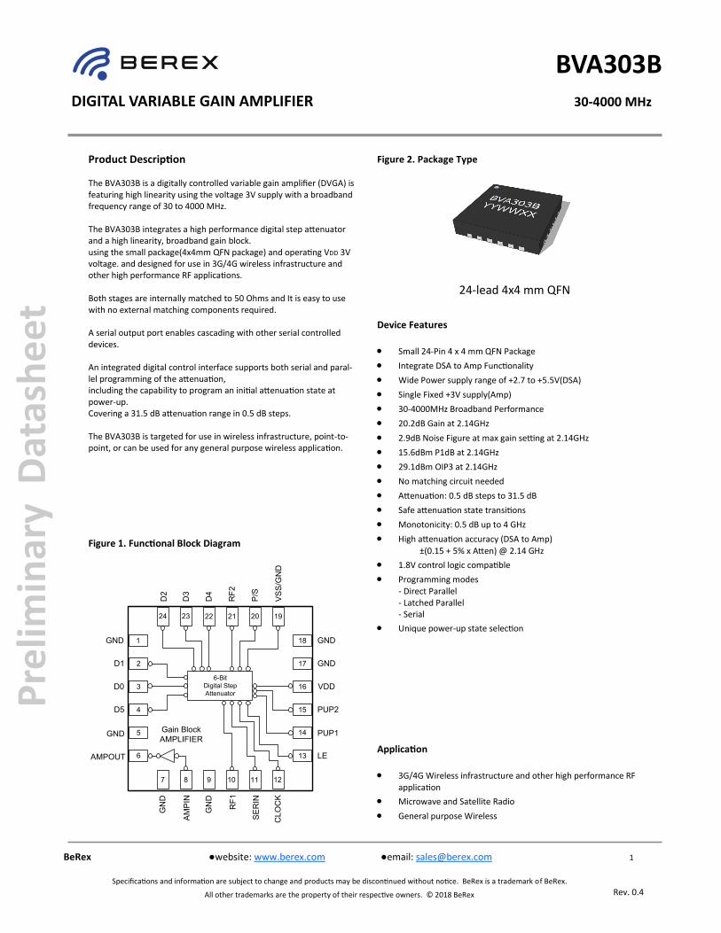
D 1 2 17 G N D 1 18 DIGITAL VARIA LE GAIN AMPLIFIER 6-B it ... · 24 D2 Parallel ontrol Voltage...
18
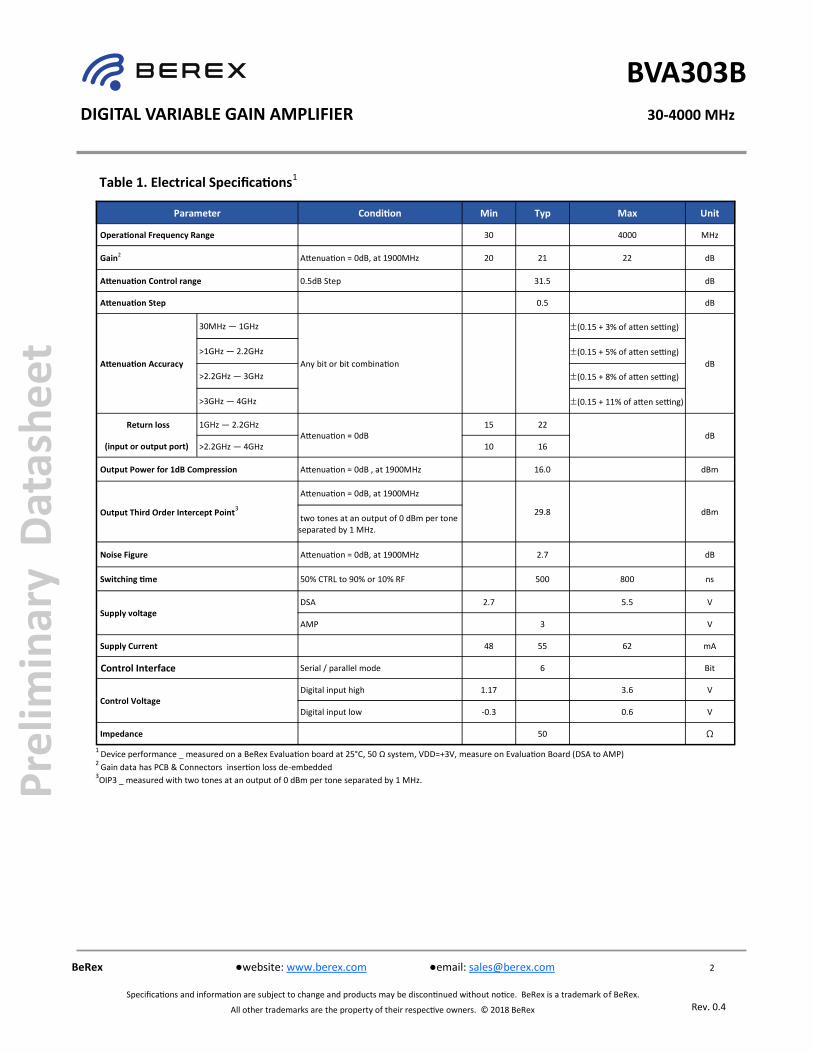
1 Rev. 0.4 BeRex ●website: www.berex.com ●email: [email protected] Specificaons and informaon are subject to change and products may be disconnued without noce. BeRex is a trademark of BeRex. All other trademarks are the property of their respecve owners. © 2018 BeRex Preliminary Datasheet DIGITAL VARIABLE GAIN AMPLIFIER 30-4000 MHz BVA303B 24-lead 4x4 mm QFN • Small 24-Pin 4 x 4 mm QFN Package • Integrate DSA to Amp Funconality • Wide Power supply range of +2.7 to +5.5V(DSA) • Single Fixed +3V supply(Amp) • 30-4000MHz Broadband Performance • 20.2dB Gain at 2.14GHz • 2.9dB Noise Figure at max gain seng at 2.14GHz • 15.6dBm P1dB at 2.14GHz • 29.1dBm OIP3 at 2.14GHz • No matching circuit needed • Aenuaon: 0.5 dB steps to 31.5 dB • Safe aenuaon state transions • Monotonicity: 0.5 dB up to 4 GHz • High aenuaon accuracy (DSA to Amp) ±(0.15 + 5% x Aen) @ 2.14 GHz • 1.8V control logic compable • Programming modes - Direct Parallel - Latched Parallel - Serial • Unique power-up state selecon • 3G/4G Wireless infrastructure and other high performance RF applicaon • Microwave and Satellite Radio • General purpose Wireless The BVA303B is a digitally controlled variable gain amplifier (DVGA) is featuring high linearity using the voltage 3V supply with a broadband frequency range of 30 to 4000 MHz. The BVA303B integrates a high performance digital step aenuator and a high linearity, broadband gain block. using the small package(4x4mm QFN package) and operang VDD 3V voltage. and designed for use in 3G/4G wireless infrastructure and other high performance RF applicaons. Both stages are internally matched to 50 Ohms and It is easy to use with no external matching components required. A serial output port enables cascading with other serial controlled devices. An integrated digital control interface supports both serial and paral- lel programming of the aenuaon, including the capability to program an inial aenuaon state at power-up. Covering a 31.5 dB aenuaon range in 0.5 dB steps. The BVA303B is targeted for use in wireless infrastructure, point-to- point, or can be used for any general purpose wireless applicaon. Figure 1. Funconal Block Diagram Device Features Figure 2. Package Type Product Descripon 1 GND D1 6-Bit Digital Step Attenuator 2 3 4 5 6 7 8 11 10 12 13 14 15 16 17 18 19 20 21 22 23 24 9 D0 D5 GND LE GND GND AMPIN RF1 SERIN CLOCK PUP1 PUP2 VDD GND GND VSS/GND RF2 P/S D4 D3 D2 AMPOUT Gain Block AMPLIFIER Applicaon
Transcript of D 1 2 17 G N D 1 18 DIGITAL VARIA LE GAIN AMPLIFIER 6-B it ... · 24 D2 Parallel ontrol Voltage...
1
Rev. 0.4
BeRex website: www.berex.com email: [email protected]
Specifications and information are subject to change and products may be discontinued without notice. BeRex is a trademark of BeRex.
All other trademarks are the property of their respective owners. © 2018 BeRex
Pre
limin
ary
Dat
ash
eet
DIGITAL VARIABLE GAIN AMPLIFIER 30-4000 MHz
BVA303B
24-lead 4x4 mm QFN
• Small 24-Pin 4 x 4 mm QFN Package
• Integrate DSA to Amp Functionality
• Wide Power supply range of +2.7 to +5.5V(DSA)
• Single Fixed +3V supply(Amp)
• 30-4000MHz Broadband Performance
• 20.2dB Gain at 2.14GHz
• 2.9dB Noise Figure at max gain setting at 2.14GHz
• 15.6dBm P1dB at 2.14GHz
• 29.1dBm OIP3 at 2.14GHz
• No matching circuit needed
• Attenuation: 0.5 dB steps to 31.5 dB
• Safe attenuation state transitions
• Monotonicity: 0.5 dB up to 4 GHz
• High attenuation accuracy (DSA to Amp)
±(0.15 + 5% x Atten) @ 2.14 GHz
• 1.8V control logic compatible
• Programming modes - Direct Parallel - Latched Parallel - Serial
• Unique power-up state selection
• 3G/4G Wireless infrastructure and other high performance RF application
• Microwave and Satellite Radio
• General purpose Wireless
The BVA303B is a digitally controlled variable gain amplifier (DVGA) is featuring high linearity using the voltage 3V supply with a broadband frequency range of 30 to 4000 MHz. The BVA303B integrates a high performance digital step attenuator and a high linearity, broadband gain block. using the small package(4x4mm QFN package) and operating VDD 3V voltage. and designed for use in 3G/4G wireless infrastructure and other high performance RF applications. Both stages are internally matched to 50 Ohms and It is easy to use with no external matching components required. A serial output port enables cascading with other serial controlled devices. An integrated digital control interface supports both serial and paral-lel programming of the attenuation, including the capability to program an initial attenuation state at power-up. Covering a 31.5 dB attenuation range in 0.5 dB steps. The BVA303B is targeted for use in wireless infrastructure, point-to-point, or can be used for any general purpose wireless application.
Figure 1. Functional Block Diagram
Device Features
Figure 2. Package Type Product Description
1GND
D1
6-Bit
Digital Step
Attenuator
2
3
4
5
6
7 8 1110 12
13
14
15
16
17
18
192021222324
9
D0
D5
GND
LE
GN
D
GN
D
AM
PIN
RF
1
SE
RIN
CL
OC
K
PUP1
PUP2
VDD
GND
GND
VS
S/G
ND
RF
2
P/S
D4
D3
D2
AMPOUT
Gain Block
AMPLIFIER
Application
2
Rev. 0.4
BeRex website: www.berex.com email: [email protected]
Specifications and information are subject to change and products may be discontinued without notice. BeRex is a trademark of BeRex.
All other trademarks are the property of their respective owners. © 2018 BeRex
Pre
limin
ary
Dat
ash
eet
DIGITAL VARIABLE GAIN AMPLIFIER 30-4000 MHz
BVA303B
Parameter Condition Min Typ Max Unit
Operational Frequency Range 30 4000 MHz
Gain2 Attenuation = 0dB, at 1900MHz 20 21 22 dB
Attenuation Control range 0.5dB Step 31.5 dB
Attenuation Step 0.5 dB
Attenuation Accuracy
30MHz — 1GHz
Any bit or bit combination
±(0.15 + 3% of atten setting)
dB
>1GHz — 2.2GHz ±(0.15 + 5% of atten setting)
>2.2GHz — 3GHz ±(0.15 + 8% of atten setting)
>3GHz — 4GHz ±(0.15 + 11% of atten setting)
Return loss 1GHz — 2.2GHz Attenuation = 0dB
15 22
dB (input or output port) >2.2GHz — 4GHz 10 16
Output Power for 1dB Compression Attenuation = 0dB , at 1900MHz 16.0 dBm
Output Third Order Intercept Point3
Attenuation = 0dB, at 1900MHz
29.8 dBm two tones at an output of 0 dBm per tone separated by 1 MHz.
Noise Figure Attenuation = 0dB, at 1900MHz 2.7 dB
Switching time 50% CTRL to 90% or 10% RF 500 800 ns
Supply voltage DSA 2.7 5.5 V
AMP 3 V
Supply Current 48 55 62 mA
Control Interface Serial / parallel mode 6 Bit
Control Voltage Digital input high 1.17 3.6 V
Digital input low -0.3 0.6 V
Impedance 50 Ω
Table 1. Electrical Specifications1
1 Device performance _ measured on a BeRex Evaluation board at 25°C, 50 Ω system, VDD=+3V, measure on Evaluation Board (DSA to AMP)
2 Gain data has PCB & Connectors insertion loss de-embedded
3OIP3 _ measured with two tones at an output of 0 dBm per tone separated by 1 MHz.
3
Rev. 0.4
BeRex website: www.berex.com email: [email protected]
Specifications and information are subject to change and products may be discontinued without notice. BeRex is a trademark of BeRex.
All other trademarks are the property of their respective owners. © 2018 BeRex
Pre
limin
ary
Dat
ash
eet
DIGITAL VARIABLE GAIN AMPLIFIER 30-4000 MHz
BVA303B
Operation of this device above any of these parameters may result in permanent damage.
Parameter Condition Min Typ Max Unit
Supply Voltage(VDD) Amp/DSA 3.6/5.5 V
Supply Current Amp 110 mA
Digital input voltage -0.3 3.6 V
Maximum input power Amp/DSA +12/+30 dBm
Operating Temperature Amp/DSA -40 85/105
Storage Temperature -55 150
Junction Temperature 150
Table 2. Typical RF Performance1
Table 3. Absolute Maximum Ratings
1 Device performance _ measured on a BeRex evaluation board at 25°C, VDD=+3V,50 Ω system. measure on Evaluation Board. (DSA to AMP)
4 OIP3 _ measured with two tones at an output of 0 dBm per tone separated by 1 MHz.
2 70MHz measured with application circuit refer to table 16. 3 Gain data has PCB & Connectors insertion loss de-embedded.
Parameter Frequency Unit
70 900 1900 2140 2650 MHz
Gain4 27.6 25.0 21.0 20.2 18.1 dB
S11 -22.4 -22.3 -18.2 -16.9 -17.1 dB
S22 -13.9 -9.3 -13.7 -12.7 -11.0 dB
OIP32 31.3 31.4 29.8 29.1 27.3 dBm
P1dB 17.1 17.6 16.0 15.6 14.5 dBm
Noise Figure 2.4 2.5 2.7 2.9 3.1 dB
4
Rev. 0.4
BeRex website: www.berex.com email: [email protected]
Specifications and information are subject to change and products may be discontinued without notice. BeRex is a trademark of BeRex.
All other trademarks are the property of their respective owners. © 2018 BeRex
Pre
limin
ary
Dat
ash
eet
DIGITAL VARIABLE GAIN AMPLIFIER 30-4000 MHz
BVA303B
Note: 1. RF pins 10 and 21 must be at 0V DC. The RF pins do not require DC blocking capacitors for proper Operation if the 0V DC requirement is met
2. Connect VssEXT (pin 19, VssEXT = GND) to enable internal negative voltage generator
1GND
Exposed Pad
2
3
4
5
D1
D0
D5
GND
6AMPOUT
7GN
D
8 9 10
11
AM
PIN
GN
D
RF1
SERIN
12
Clo
ck
18 GND
17
16
15
14
GND
VDD
PUP2
PUP1
13 LE
24
D2
23
22
21
20
D3
D4
RF2 P/S
19
VSS/G
ND
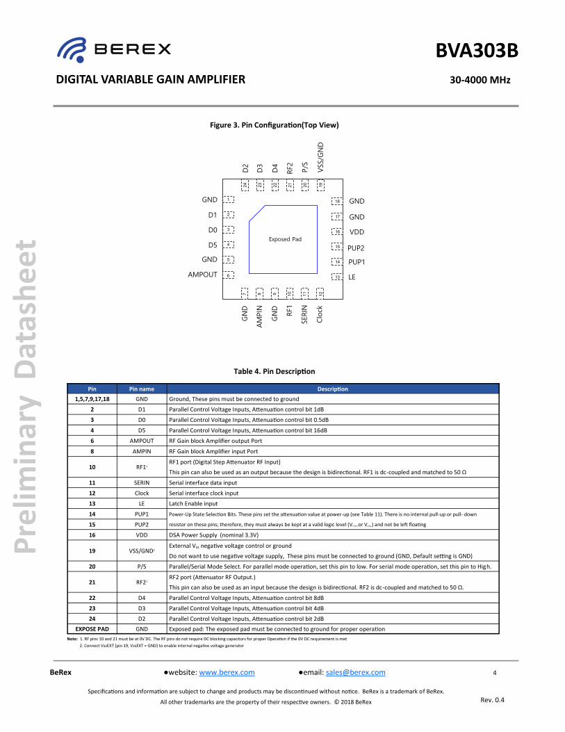
Table 4. Pin Description
Figure 3. Pin Configuration(Top View)
Pin Pin name Description
1,5,7,9,17,18 GND Ground, These pins must be connected to ground
2 D1 Parallel Control Voltage Inputs, Attenuation control bit 1dB
3 D0 Parallel Control Voltage Inputs, Attenuation control bit 0.5dB
4 D5 Parallel Control Voltage Inputs, Attenuation control bit 16dB
6 AMPOUT RF Gain block Amplifier output Port
8 AMPIN RF Gain block Amplifier input Port
10 RF11 RF1 port (Digital Step Attenuator RF Input)
This pin can also be used as an output because the design is bidirectional. RF1 is dc-coupled and matched to 50 Ω
11 SERIN Serial interface data input
12 Clock Serial interface clock input
13 LE Latch Enable input
14 PUP1 Power-Up State Selection Bits. These pins set the attenuation value at power-up (see Table 11). There is no internal pull-up or pull- down
15 PUP2 resistor on these pins; therefore, they must always be kept at a valid logic level (VCTLH or VCTLL) and not be left floating
16 VDD DSA Power Supply (nominal 3.3V)
19 VSS/GND2 External VSS negative voltage control or ground
Do not want to use negative voltage supply, These pins must be connected to ground (GND, Default setting is GND)
20 P/S Parallel/Serial Mode Select. For parallel mode operation, set this pin to low. For serial mode operation, set this pin to High.
21 RF21 RF2 port (Attenuator RF Output.)
This pin can also be used as an input because the design is bidirectional. RF2 is dc-coupled and matched to 50 Ω.
22 D4 Parallel Control Voltage Inputs, Attenuation control bit 8dB
23 D3 Parallel Control Voltage Inputs, Attenuation control bit 4dB
24 D2 Parallel Control Voltage Inputs, Attenuation control bit 2dB
EXPOSE PAD GND Exposed pad: The exposed pad must be connected to ground for proper operation
5
Rev. 0.4
BeRex website: www.berex.com email: [email protected]
Specifications and information are subject to change and products may be discontinued without notice. BeRex is a trademark of BeRex.
All other trademarks are the property of their respective owners. © 2018 BeRex
Pre
limin
ary
Dat
ash
eet
DIGITAL VARIABLE GAIN AMPLIFIER 30-4000 MHz
BVA303B
BVA303B can be programmed using either the parallel or serial inter-face, which is selectable via P/S pin(Pin20). Serial mode is selected by floating P/S or pulling it to a voltage logic high and parallel mode is selected by setting P/S to logic low Serial Control Mode
The serial interface is a 6 bit shift register to shift in the data MSB (D5) first. When serial programming is used, all the parallel control input pins (2,3,4,22,23,24) must be grounded. (Max Gain state). It is controlled by three CMOS-compatible signals: SERIN, Clock, and Latch Enable (LE).
D5 Attenuation 16dB Control Bit
D4 Attenuation 8dB Control Bit
D3 Attenuation 4dB Control Bit
D2 Attenuation 2dB Control Bit
D1 Attenuation 1dB Control Bit
D0 Attenuation 0.5dB Control Bit
The BVA303B has a 3-wire serial peripheral interface (SPI): serial data input (Data), clock (CLK), and latch enable (LE). The serial control inter-face is activated when P/S is set to HIGH. In serial mode, the 6-bit Data is clocked MSB first on the rising CLK edges into the shift register and then LE must be toggled High to latch the new attenuation state into the device. LE must be set to low to clock new 6-bit data into the shift register because CLK is masked to prevent the attenuator value from changing if LE is kept High (see Figure 4 and Table 8).
Programming Options
Figure 4. Serial Mode Resister Timing Diagram
Table 5. 6-Bit Serial Word Sequence
Table 7. Serial Interface Timing Specifications
Table 8. Truth Table for Serial Control Word Table 6. Mode Selection
D5X X D[5:0]NEXT WORD XD4 D3 D2 D1 D0
X
tSH
tSStSCK
tLNtLEW
tLES
MSB[FIRST IN]
LSB[LAST IN]
P/S
SERIAL IN
CLK
LE
P/S Control Mode
LOW Parallel
HIGH Serial
Symbol Parameter Min Typ Max Unit
fClk Serial data clock frequency 10 MHz
tSCK Minimum serial period 70
tSS Serial Data setup time 10
tSH Serial Data hold time 10
tLN LE setup time 10
tLEW Minimum LE pulse width 30
tLES Minimum LE pulse spacing 600
Digital Control Input Attenuation
D5 D4 D3 D2 D1 D0
(MSB) (LSB) (dB)
LOW LOW LOW LOW LOW LOW 0 (Reference)
LOW LOW LOW LOW LOW HIGH 0.5
LOW LOW LOW LOW HIGH LOW 1
LOW LOW LOW HIGH LOW LOW 2
LOW LOW HIGH LOW LOW LOW 4
LOW HIGH LOW LOW LOW LOW 8
HIGH LOW LOW LOW LOW LOW 16
HIGH HIGH HIGH HIGH HIGH HIGH 31.5
6
Rev. 0.4
BeRex website: www.berex.com email: [email protected]
Specifications and information are subject to change and products may be discontinued without notice. BeRex is a trademark of BeRex.
All other trademarks are the property of their respective owners. © 2018 BeRex
Pre
limin
ary
Dat
ash
eet
DIGITAL VARIABLE GAIN AMPLIFIER 30-4000 MHz
BVA303B
Figure 5. Latched Parallel Mode Timing Diagram
Parallel Control Mode
The BVA303B has six digital control inputs, D0 (LSB) to D5 (MSB), to select the desired attenuation state in parallel mode, as shown in Table 9. The parallel control interface is activated when P/S is set to low. There are two modes of parallel operation: direct parallel and latched parallel Direct Parallel Mode The LE pin must be kept LOW. The attenuation state is changed by the control voltage inputs (D0 to D5) directly. This mode is ideal for man-ual control of the attenuator. In this mode the device will immediate-ly react to any voltage changes to the parallel control pins [pins 2, 3, 4, 22,23, 24]. Use direct parallel mode for the fastest settling time. Latched Parallel Mode The LE pin must be kept low when changing the control voltage inputs (D0 to D5) to set the attenuation state. When the desired state is set, LE must be toggled LOW to transfer the 6-bit data to the bypass switches of the attenuator array, and then toggled low to latch the change into the device until the next desired attenuation change (see Figure 5 and Table 9).
Table 10. Parallel Interface Timing Specifications
X
tPHtPS
P/S
Parallel IN
LE
XD[5:0]
PARALLELCONTROL
tLEW
X
Table 9. Truth Table for the Parallel Control Word
D0 D1 D2 D3 D4 D5 P/S LE Attenuation State
LOW LOW LOW LOW LOW LOW LOW HIGH Reference Loss
HIGH LOW LOW LOW LOW LOW LOW HIGH 0.5dB
LOW HIGH LOW LOW LOW LOW LOW HIGH 1dB
LOW LOW HIGH LOW LOW LOW LOW HIGH 2dB
LOW LOW LOW HIGH LOW LOW LOW HIGH 4dB
LOW LOW LOW LOW HIGH LOW LOW HIGH 8dB
LOW LOW LOW LOW LOW HIGH LOW HIGH 16dB
HIGH HIGH HIGH HIGH HIGH HIGH LOW HIGH 31.5dB
Symbol Parameter Min Typ Max Unit
tLEW Minimum LE pulse width 10 ns
tPH Data hold time from LE 10 ns
tPS Data setup time to LE 10 ns
Table 11. PUP Truth Table for Parallel Control Mode
Power-UP Interface The BVA303B uses the PUP1 and PUP2 control voltage inputs to set the attenuation value to a known value at power-up before the initial control data word is provided in parallel mode. Power-up Control for Parallel Mode (P/S=LOW) When the attenuator powers up with LE set to low, the state of PUP1 and PUP2 determines the power-up state of the device per the truth table shown in Table 11. Power-up Control for Serial Mode (P/S=HIGH) When the attenuator powers up in Serial mode, the six digital control inputs are set to whatever data is present on the six parallel data inputs (D0 to D5, Refer to Table 12). This allows any one of the 64 attenuation settings to be specified as the power-up state.
Attenuation state P/S LE PUP1 PUP2
31.5 dB LOW LOW HIGH HIGH
16 dB LOW LOW HIGH LOW
8 dB LOW LOW LOW HIGH
Reference Loss LOW LOW LOW LOW
Defined by C0.5-C16 LOW HIGH Don’t Care Don’t Care
Attenuation State P/S D0 D1 D2 D3 D4 D5
Reference Loss HIGH LOW LOW LOW LOW LOW LOW
0.5dB HIGH HIGH LOW LOW LOW LOW LOW
1dB HIGH LOW HIGH LOW LOW LOW LOW
2dB HIGH LOW LOW HIGH LOW LOW LOW
4dB HIGH LOW LOW LOW HIGH LOW LOW
8dB HIGH LOW LOW LOW LOW HIGH LOW
16dB HIGH LOW LOW LOW LOW LOW HIGH
20dB HIGH LOW LOW LOW HIGH LOW HIGH
24dB HIGH LOW LOW LOW LOW HIGH HIGH
31.5dB HIGH HIGH HIGH HIGH HIGH HIGH HIGH
Table 12. PUP Truth Table for Serial Control Mode
7
Rev. 0.4
BeRex website: www.berex.com email: [email protected]
Specifications and information are subject to change and products may be discontinued without notice. BeRex is a trademark of BeRex.
All other trademarks are the property of their respective owners. © 2018 BeRex
Pre
limin
ary
Dat
ash
eet
DIGITAL VARIABLE GAIN AMPLIFIER 30-4000 MHz
BVA303B
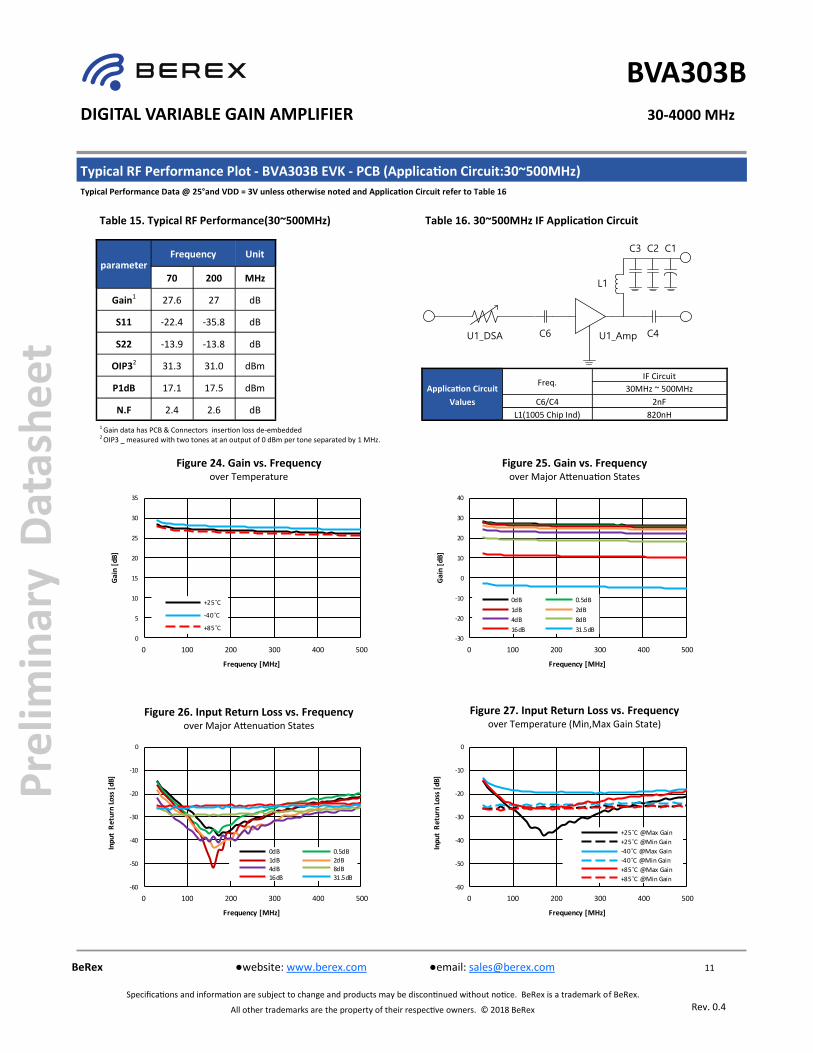
Table 13. Typical RF Performance(500~4000MHz)
Application Circuit
Values
Freq. RF Circuit
500MHz ~ 4000MHz
C6/C4 20pF
L1(1005 Chip Ind) 22nH
Typical Performance Data @ 25°and VDD = 3V unless otherwise noted and Application Circuit refer to Table 14
Typical RF Performance Plot - BVA303B EVK - PCB (Application Circuit:500~4000MHz)
Table 14. 500~4000MHz RF Application Circuit
parameter Frequency Unit
500 900 1900 2140 2650 MHz
Gain1 25.3 25.0 21.0 20.2 18.1 dB
S11 -12.4 -22.3 -18.2 -16.9 -17.1 dB
S22 -7.0 -9.3 -13.7 -12.7 -11.0 dB
OIP32 30.8 31.4 29.8 29.1 27.3 dBm
P1dB 17.9 17.6 16.0 15.6 14.5 dBm
N.F 2.5 2.5 2.7 2.9 3.1 dB
Figure 6. Gain vs. Frequency over Temperature (Max Gain State)
Figure 8. Input Return Loss vs. Frequency over Major Attenuation States
Figure 7. Gain vs. Frequency over Major Attenuation States
Figure 9. Input Return Loss vs. Frequency over Temperature (Min1,Max Gain State)
* 1Min Gain was measured in the state is set with attenuation 31.5dB.
0
5
10
15
20
25
30
500 1,000 1,500 2,000 2,500 3,000 3,500 4,000
Gai
n [d
B]
Frequency [MHz]
+25˚C
-40˚C
+85˚C
-30
-20
-10
0
10
20
30
500 1,000 1,500 2,000 2,500 3,000 3,500 4,000
Ga
in [
dB
]
Frequency [MHz]
0dB 0.5dB
1dB 2dB
4dB 8dB
16dB 31.5dB
-50
-40
-30
-20
-10
0
500 1,000 1,500 2,000 2,500 3,000 3,500 4,000
Inp
ut
Re
turn
Lo
ss [
dB
]
Frequency [MHz]
0dB 0.5dB
1dB 2dB
4dB 8dB
16dB 31.5dB-50
-40
-30
-20
-10
0
500 1,000 1,500 2,000 2,500 3,000 3,500 4,000
Inpu
t R
etur
n Lo
ss [
dB]
Frequency [MHz]
+25˚C @Max Gain
+25˚C @Min Gain
-40˚C @Max Gain
-40˚C @Min Gain
+85˚C @Max Gain
+85˚C @Min Gain
1 Gain data has PCB & Connectors insertion loss de-embedded 2 OIP3 _ measured with two tones at an output of 0 dBm per tone separated by 1 MHz.
U1_AmpC6
L1
C4
C2C3 C1
U1_DSA
8
Rev. 0.4
BeRex website: www.berex.com email: [email protected]
Specifications and information are subject to change and products may be discontinued without notice. BeRex is a trademark of BeRex.
All other trademarks are the property of their respective owners. © 2018 BeRex
Pre
limin
ary
Dat
ash
eet
DIGITAL VARIABLE GAIN AMPLIFIER 30-4000 MHz
BVA303B
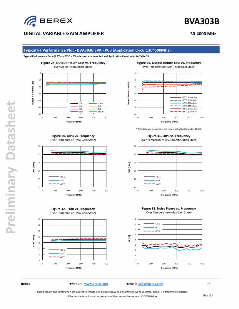
Figure 10. Output Return Loss vs. Frequency over Major Attenuation States
Figure 11. Output Return Loss vs. Frequency over Temperature (Min1, Max Gain State)
Figure 12. OIP3 vs. Frequency Over Temperature (Max Gain State)
Figure 14. P1dB vs. Frequency Over Temperature (Max Gain State)
Figure 13. OIP3 vs. Frequency Over Temperature (15.5dB Atteuation State)
Figure 15. Noise Figure vs. Frequency Over Temperature (Max Gain State)
* 1Min Gain was measured in the state is set with attenuation 31.5dB.
-50
-40
-30
-20
-10
0
500 1,000 1,500 2,000 2,500 3,000 3,500 4,000
Out
put
Ret
urn
Loss
[dB
]
Frequency [MHz]
0dB 0.5dB1dB 2dB4dB 8dB16dB 31.5dB
-40
-30
-20
-10
0
500 1,000 1,500 2,000 2,500 3,000 3,500 4,000
Ou
tpu
t R
etu
rn L
oss
[d
B]
Frequency [MHz]
+25˚C @Max Gain+25˚C @Min Gain-40˚C @Max Gain-40˚C @Min Gain+85˚C @Max Gain+85˚C @Min Gain
0
5
10
15
20
25
30
35
500 1,000 1,500 2,000 2,500 3,000 3,500 4,000
P1dB
[dB
m]
Frequency [MHz]
+25˚C
-40˚C
+85˚C
0
1
2
3
4
5
6
7
8
500 1,000 1,500 2,000 2,500 3,000 3,500 4,000
NF
[dB]
Frequency [MHz]
+25˚C
-40˚C
+85˚C
0
5
10
15
20
25
30
35
500 1,000 1,500 2,000 2,500 3,000 3,500 4,000
OIP
3 [
dB
m]
Frequency [MHz]
+25˚C
-40˚C
+85˚C
0
5
10
15
20
25
30
35
500 1,000 1,500 2,000 2,500 3,000 3,500 4,000
OIP
3 [
dB
m]
Frequency [MHz]
+25˚C
-40˚C
+85˚C
Typical Performance Data @ 25°and VDD = 3V unless otherwise noted and Application Circuit refer to Table 14
Typical RF Performance Plot - BVA303B EVK - PCB (Application Circuit:500~4000MHz)
9
Rev. 0.4
BeRex website: www.berex.com email: [email protected]
Specifications and information are subject to change and products may be discontinued without notice. BeRex is a trademark of BeRex.
All other trademarks are the property of their respective owners. © 2018 BeRex
Pre
limin
ary
Dat
ash
eet
DIGITAL VARIABLE GAIN AMPLIFIER 30-4000 MHz
BVA303B
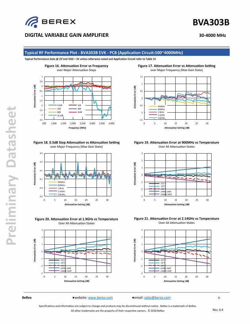
Figure 16. Attenuation Error vs Frequency over Major Attenuation Steps
Figure 17. Attenuation Error vs Attenuation Setting over Major Frequency (Max Gain State)
Figure 18. 0.5dB Step Attenuation vs Attenuation Setting over Major Frequency (Max Gain State)
Figure 20. Attenuation Error at 1.9GHz vs Temperature Over All Attenuation States
Figure 19. Attenuation Error at 900MHz vs Temperature Over All Attenuation States
Figure 21. Attenuation Error at 2.14GHz vs Temperature Over All Attenuation States
-3
-2
-1
0
1
2
3
0 5 10 15 20 25 30
Att
enua
tion
Err
or [
dB]
Attenuation Setting [dB]
+25˚C
-40˚C
+85˚C
UPPER LIMIT
LOWER LIMIT
-3
-2
-1
0
1
2
3
0 5 10 15 20 25 30
Att
enua
tion
Err
or [
dB]
Attenuation Setting [dB]
+25˚C
-40˚C
+85˚C
UPPER LIMIT
LOWER LIMIT-3
-2
-1
0
1
2
3
0 5 10 15 20 25 30
Att
enua
tion
Err
or [
dB]
Attenuation Setting [dB]
+25˚C
-40˚C
+85˚C
UPPER LIMIT
LOWER LIMIT
-3.5
-3
-2.5
-2
-1.5
-1
-0.5
0
0.5
1
500 1,000 1,500 2,000 2,500 3,000 3,500 4,000
Att
enu
atio
n E
rro
r [d
B]
Frequency [MHz]
0.5dB 1dB
2dB 4dB
8dB 16dB
31.5dB
-1.5
-1
-0.5
0
0.5
1
1.5
0 5 10 15 20 25 30
Att
enua
tio
n Er
ror
[dB]
Attenuation Setting [dB]
500MHz
900MHz
1.9GHz
2.14GHz
2.65GHz
-0.5
-0.3
-0.1
0.1
0.3
0.5
0 5 10 15 20 25 30
Att
enua
tio
n Er
ror
[dB]
Attenuation Setting [dB]
500MHz
900MHz
1.9GHz
2.14GHz
2.65GHz
Typical Performance Data @ 25°and VDD = 3V unless otherwise noted and Application Circuit refer to Table 14
Typical RF Performance Plot - BVA303B EVK - PCB (Application Circuit:500~4000MHz)
10
Rev. 0.4
BeRex website: www.berex.com email: [email protected]
Specifications and information are subject to change and products may be discontinued without notice. BeRex is a trademark of BeRex.
All other trademarks are the property of their respective owners. © 2018 BeRex
Pre
limin
ary
Dat
ash
eet
DIGITAL VARIABLE GAIN AMPLIFIER 30-4000 MHz
BVA303B
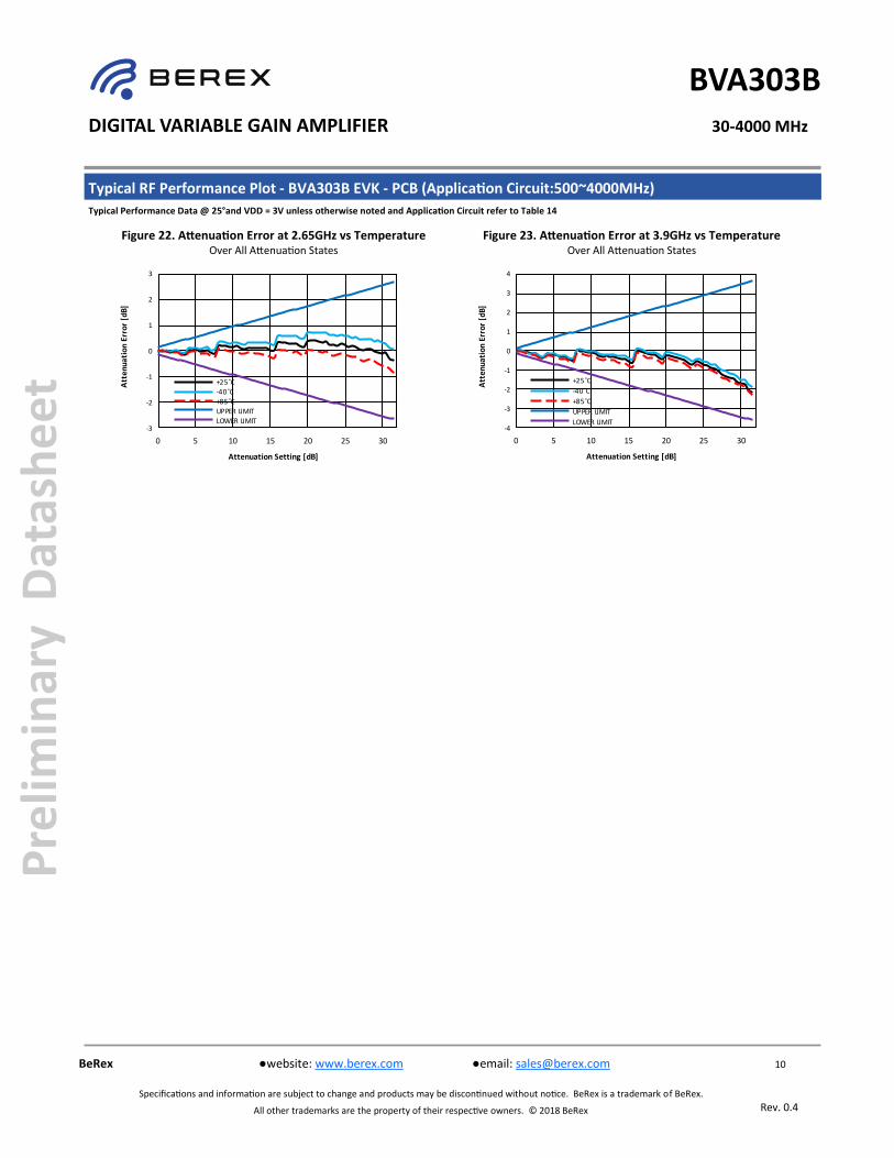
Figure 22. Attenuation Error at 2.65GHz vs Temperature Over All Attenuation States
Figure 23. Attenuation Error at 3.9GHz vs Temperature Over All Attenuation States
-3
-2
-1
0
1
2
3
0 5 10 15 20 25 30
Att
enua
tion
Err
or [
dB]
Attenuation Setting [dB]
+25˚C
-40˚C
+85˚C
UPPER LIMIT
LOWER LIMIT-4
-3
-2
-1
0
1
2
3
4
0 5 10 15 20 25 30
Att
enua
tio
n Er
ror
[dB]
Attenuation Setting [dB]
+25˚C
-40˚C
+85˚C
UPPER LIMIT
LOWER LIMIT
Typical Performance Data @ 25°and VDD = 3V unless otherwise noted and Application Circuit refer to Table 14
Typical RF Performance Plot - BVA303B EVK - PCB (Application Circuit:500~4000MHz)
11
Rev. 0.4
BeRex website: www.berex.com email: [email protected]
Specifications and information are subject to change and products may be discontinued without notice. BeRex is a trademark of BeRex.
All other trademarks are the property of their respective owners. © 2018 BeRex
Pre
limin
ary
Dat
ash
eet
DIGITAL VARIABLE GAIN AMPLIFIER 30-4000 MHz
BVA303B
Table 15. Typical RF Performance(30~500MHz)
Application Circuit
Values
Freq. IF Circuit
30MHz ~ 500MHz
C6/C4 2nF
L1(1005 Chip Ind) 820nH
Typical Performance Data @ 25°and VDD = 3V unless otherwise noted and Application Circuit refer to Table 16
Typical RF Performance Plot - BVA303B EVK - PCB (Application Circuit:30~500MHz)
Table 16. 30~500MHz IF Application Circuit
parameter Frequency Unit
70 200 MHz
Gain1 27.6 27 dB
S11 -22.4 -35.8 dB
S22 -13.9 -13.8 dB
OIP32 31.3 31.0 dBm
P1dB 17.1 17.5 dBm
N.F 2.4 2.6 dB
Figure 24. Gain vs. Frequency over Temperature
Figure 26. Input Return Loss vs. Frequency over Major Attenuation States
Figure 25. Gain vs. Frequency over Major Attenuation States
Figure 27. Input Return Loss vs. Frequency over Temperature (Min,Max Gain State)
0
5
10
15
20
25
30
35
0 100 200 300 400 500
Ga
in [
dB
]
Frequency [MHz]
+25˚C
-40˚C
+85˚C
-30
-20
-10
0
10
20
30
40
0 100 200 300 400 500
Ga
in [
dB
]
Frequency [MHz]
0dB 0.5dB
1dB 2dB
4dB 8dB
16dB 31.5dB
-60
-50
-40
-30
-20
-10
0
0 100 200 300 400 500
Inp
ut
Re
turn
Lo
ss [
dB
]
Frequency [MHz]
0dB 0.5dB1dB 2dB4dB 8dB16dB 31.5dB
-60
-50
-40
-30
-20
-10
0
0 100 200 300 400 500
Inp
ut
Re
turn
Lo
ss [
dB
]
Frequency [MHz]
+25˚C @Max Gain
+25˚C @Min Gain
-40˚C @Max Gain
-40˚C @Min Gain
+85˚C @Max Gain
+85˚C @Min Gain
1 Gain data has PCB & Connectors insertion loss de-embedded 2 OIP3 _ measured with two tones at an output of 0 dBm per tone separated by 1 MHz.
U1_AmpC6
L1
C4
C2C3 C1
U1_DSA
12
Rev. 0.4
BeRex website: www.berex.com email: [email protected]
Specifications and information are subject to change and products may be discontinued without notice. BeRex is a trademark of BeRex.
All other trademarks are the property of their respective owners. © 2018 BeRex
Pre
limin
ary
Dat
ash
eet
DIGITAL VARIABLE GAIN AMPLIFIER 30-4000 MHz
BVA303B
Figure 28. Output Return Loss vs. Frequency over Major Attenuation States
Figure 29. Output Return Loss vs. Frequency over Temperature (Min1, Max Gain State)
Figure 30. OIP3 vs. Frequency Over Temperature (Max Gain State)
Figure 32. P1dB vs. Frequency Over Temperature (Max Gain State)
Figure 31. OIP3 vs. Frequency Over Temperature (15.5dB Atteuation State)
Figure 33. Noise Figure vs. Frequency Over Temperature (Max Gain State)
* 1Min Gain was measured in the state is set with attenuation 31.5dB.
-60
-50
-40
-30
-20
-10
0
0 100 200 300 400 500
Ou
tpu
t R
etu
rn L
oss
[d
B]
Frequency [MHz]
0dB 0.5dB
1dB 2dB
4dB 8dB
16dB 31.5dB-60
-50
-40
-30
-20
-10
0
0 100 200 300 400 500
Ou
tpu
t R
etu
rn L
oss
[d
B]
Frequency [MHz]
+25˚C @Max Gain
+25˚C @Min Gain
-40˚C @Max Gain
-40˚C @Min Gain
+85˚C @Max Gain
+85˚C @Min Gain
10
15
20
25
30
35
0 100 200 300 400 500
OIP
3 [
dB
m]
Frequency [MHz]
+25˚C
-40˚C
+85˚C
10
15
20
25
30
35
0 100 200 300 400 500
OIP
3 [
dB
m]
Frequency [MHz]
+25˚C
-40˚C
+85˚C
0
5
10
15
20
25
30
35
0 100 200 300 400 500
P1
dB
[d
Bm
]
Frequency [MHz]
+25˚C
-40˚C
+85˚C
0
1
2
3
4
5
6
7
8
0 100 200 300 400 500
NF
[d
B]
Frequency [MHz]
+25˚C
-40˚C
+85˚C
Typical Performance Data @ 25°and VDD = 3V unless otherwise noted and Application Circuit refer to Table 16
Typical RF Performance Plot - BVA303B EVK - PCB (Application Circuit:30~500MHz)
13
Rev. 0.4
BeRex website: www.berex.com email: [email protected]
Specifications and information are subject to change and products may be discontinued without notice. BeRex is a trademark of BeRex.
All other trademarks are the property of their respective owners. © 2018 BeRex
Pre
limin
ary
Dat
ash
eet
DIGITAL VARIABLE GAIN AMPLIFIER 30-4000 MHz
BVA303B
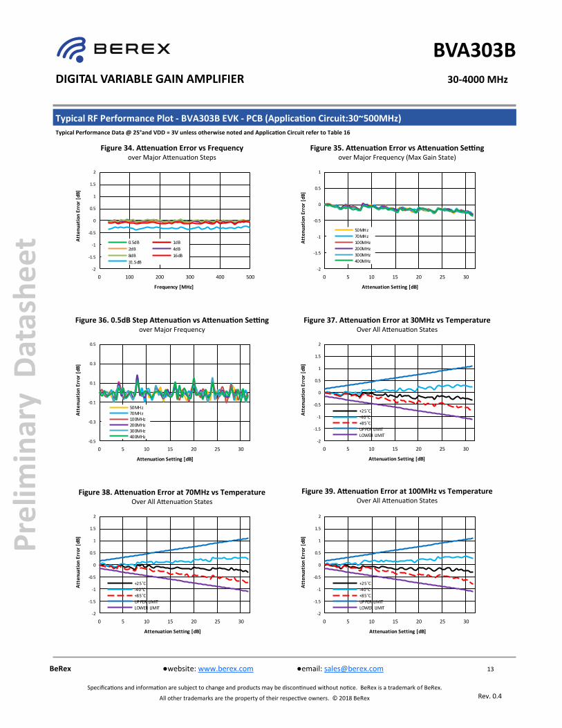
Figure 34. Attenuation Error vs Frequency over Major Attenuation Steps
Figure 35. Attenuation Error vs Attenuation Setting over Major Frequency (Max Gain State)
Figure 36. 0.5dB Step Attenuation vs Attenuation Setting over Major Frequency
Figure 38. Attenuation Error at 70MHz vs Temperature Over All Attenuation States
Figure 37. Attenuation Error at 30MHz vs Temperature Over All Attenuation States
Figure 39. Attenuation Error at 100MHz vs Temperature Over All Attenuation States
-2
-1.5
-1
-0.5
0
0.5
1
0 5 10 15 20 25 30
Att
enua
tio
n Er
ror
[dB]
Attenuation Setting [dB]
50MHz
70MHz
100MHz
200MHz
300MHz
400MHz
-0.5
-0.3
-0.1
0.1
0.3
0.5
0 5 10 15 20 25 30
Att
enua
tio
n Er
ror
[dB]
Attenuation Setting [dB]
50MHz70MHz100MHz200MHz300MHz400MHz
-2
-1.5
-1
-0.5
0
0.5
1
1.5
2
0 5 10 15 20 25 30
Att
enua
tion
Err
or [
dB]
Attenuation Setting [dB]
+25˚C
-40˚C
+85˚CUPPER LIMIT
LOWER LIMIT
-2
-1.5
-1
-0.5
0
0.5
1
1.5
2
0 5 10 15 20 25 30
Att
enua
tio
n Er
ror
[dB]
Attenuation Setting [dB]
+25˚C
-40˚C
+85˚C
UPPER LIMIT
LOWER LIMIT-2
-1.5
-1
-0.5
0
0.5
1
1.5
2
0 5 10 15 20 25 30
Att
enua
tio
n Er
ror
[dB]
Attenuation Setting [dB]
+25˚C
-40˚C
+85˚C
UPPER LIMIT
LOWER LIMIT
-2
-1.5
-1
-0.5
0
0.5
1
1.5
2
0 100 200 300 400 500
Att
enu
atio
n E
rro
r [d
B]
Frequency [MHz]
0.5dB 1dB
2dB 4dB
8dB 16dB
31.5dB
Typical Performance Data @ 25°and VDD = 3V unless otherwise noted and Application Circuit refer to Table 16
Typical RF Performance Plot - BVA303B EVK - PCB (Application Circuit:30~500MHz)
14
Rev. 0.4
BeRex website: www.berex.com email: [email protected]
Specifications and information are subject to change and products may be discontinued without notice. BeRex is a trademark of BeRex.
All other trademarks are the property of their respective owners. © 2018 BeRex
Pre
limin
ary
Dat
ash
eet
DIGITAL VARIABLE GAIN AMPLIFIER 30-4000 MHz
BVA303B
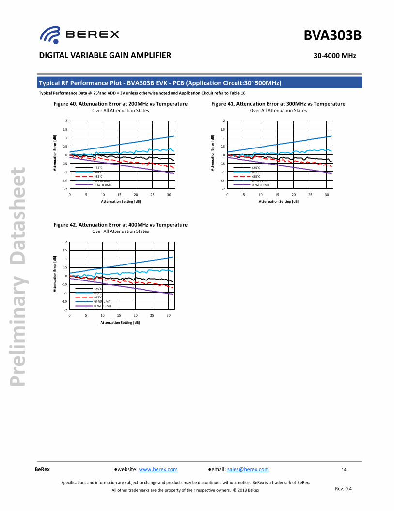
Figure 40. Attenuation Error at 200MHz vs Temperature Over All Attenuation States
Figure 41. Attenuation Error at 300MHz vs Temperature Over All Attenuation States
Figure 42. Attenuation Error at 400MHz vs Temperature Over All Attenuation States
-2
-1.5
-1
-0.5
0
0.5
1
1.5
2
0 5 10 15 20 25 30
Att
enua
tio
n Er
ror
[dB]
Attenuation Setting [dB]
+25˚C
-40˚C
+85˚C
UPPER LIMIT
LOWER LIMIT-2
-1.5
-1
-0.5
0
0.5
1
1.5
2
0 5 10 15 20 25 30
Att
enua
tio
n Er
ror
[dB]
Attenuation Setting [dB]
+25˚C
-40˚C
+85˚C
UPPER LIMIT
LOWER LIMIT
-2
-1.5
-1
-0.5
0
0.5
1
1.5
2
0 5 10 15 20 25 30
Att
enua
tio
n Er
ror
[dB]
Attenuation Setting [dB]
+25˚C
-40˚C
+85˚C
UPPER LIMIT
LOWER LIMIT
Typical Performance Data @ 25°and VDD = 3V unless otherwise noted and Application Circuit refer to Table 16
Typical RF Performance Plot - BVA303B EVK - PCB (Application Circuit:30~500MHz)
15
Rev. 0.4
BeRex website: www.berex.com email: [email protected]
Specifications and information are subject to change and products may be discontinued without notice. BeRex is a trademark of BeRex.
All other trademarks are the property of their respective owners. © 2018 BeRex
Pre
limin
ary
Dat
ash
eet
DIGITAL VARIABLE GAIN AMPLIFIER 30-4000 MHz
BVA303B
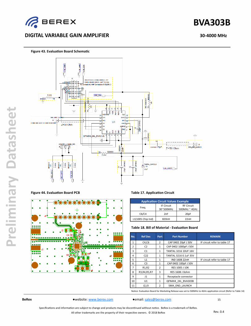
Figure 43. Evaluation Board Schematic
Application Circuit Values Example
Freq. IF Circuit
30~500MHz RF Circuit
500MHz ~ 4GHz
C6/C4 2nF 20pF
L1(1005 Chip Ind) 820nH 22nH
Table 17. Application Circuit
Table 18. Bill of Material - Evaluation Board
No. Ref Des Part Part Number REMARK
1 C4,C6 2 CAP 0402 20pF J 50V IF circuit refer to table 17
2 C2 1 CAP 0402 1000pF J 50V
3 C1 1 TANTAL 3216 10UF 16V
4 C22 1 TANTAL 3216 0.1uF 35V
5 L1 1 IND 1608 22nH IF circuit refer to table 17
6 C3 1 CAP 0402 100pF J 50V
7 R1,R2 2 RES 1005 J 10K
8 R3,R4,R5,R7 3 RES 1608 J 0ohm
9 J1 1 Receptacle connector
10 U1 1 QFN4X4_24L_BVA303B
11 J2,J3 2 SMA_END_LAUNCH
Notice: Evaluation Board for Marketing Release was set to 500MHz to 4GHz application circuit (Refer to Table 14)
Figure 44. Evaluation Board PCB
16
Rev. 0.4
BeRex website: www.berex.com email: [email protected]
Specifications and information are subject to change and products may be discontinued without notice. BeRex is a trademark of BeRex.
All other trademarks are the property of their respective owners. © 2018 BeRex
Pre
limin
ary
Dat
ash
eet
DIGITAL VARIABLE GAIN AMPLIFIER 30-4000 MHz
BVA303B
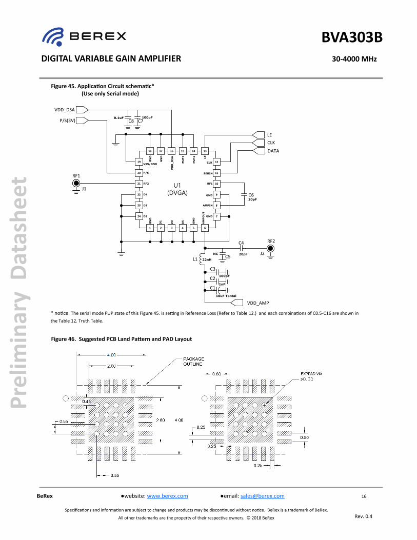
Figure 45. Application Circuit schematic* (Use only Serial mode)
* notice. The serial mode PUP state of this Figure 45. is setting in Reference Loss (Refer to Table 12.) and each combinations of C0.5-C16 are shown in
the Table 12. Truth Table.
Figure 46. Suggested PCB Land Pattern and PAD Layout
U1(DVGA)
RF1
19
20
21
22
23
1 2 3 4 5
1318 17 16 15 14
CLK
DATA
RF2
P/S
C3
J1
J2L1
LE
VDD_DSA
24
6
12
11
10
9
8
7
VDD_AMP
VSS/GNDG
ND
GN
D
VD
D_
DS
A
PU
P1
PU
P2 LE
CLK
SERIN
GND
GND
RF1
AMPINA
MP
OU
T
GN
D
D5
D0
D1
GN
D
D2
D3
D4
RF2
C2
C1
C6
C7C8
C5
C4
P/S(3V)
100pF
1nF
10uF Tantal
NC 20pF
22nH
20pF
100pF0.1uF
17
Rev. 0.4
BeRex website: www.berex.com email: [email protected]
Specifications and information are subject to change and products may be discontinued without notice. BeRex is a trademark of BeRex.
All other trademarks are the property of their respective owners. © 2018 BeRex
Pre
limin
ary
Dat
ash
eet
DIGITAL VARIABLE GAIN AMPLIFIER 30-4000 MHz
BVA303B
Figure 47. Package Outline Dimension
Figure 48. Evaluation Board PCB Layer Information
COPPER :1oz + 0.5oz (plating), Top Layer
COPPER :1oz (GND), Inner Layer
COPPER :1oz + 0.5oz (plating), Bottom Layer
P.P : (0.2+0.06+0.06) TOTAL = 0.32mm
CORE : 0.73mm FINISH TICKNESS :1.55T
P.P : (0.2+0.06+0.06) TOTAL = 0.32mm
COPPER :1oz, Inner Layer
EM825B ER: 4.6~4.8
MTC Er:4.6
EM825B Er:4.6~4.8
18
Rev. 0.4
BeRex website: www.berex.com email: [email protected]
Specifications and information are subject to change and products may be discontinued without notice. BeRex is a trademark of BeRex.
All other trademarks are the property of their respective owners. © 2018 BeRex
Pre
limin
ary
Dat
ash
eet
DIGITAL VARIABLE GAIN AMPLIFIER 30-4000 MHz
BVA303B
Figure 49. Tape & Reel
NATO CAGE code:
2 N 9 6 F
BVA303BYYWWXX
Figure 50. Package Marking
Lead plating finish
100% Tin Matte finish
MSL / ESD Rating
ESD Rating:
Value:
Test:
Standard:
MSL Rating:
Standard:
Class 1C
Passes ≤ 2000V
Human Body Model(HBM)
JEDEC Standard JESD22-A114B
Level 1 at +265°C convection reflow
JEDEC Standard J-STD-020 Proper ESD procedures should be followed when handling this device.
C a u t i o n : ESD SensitiveAppropriate precautions in handling, packaging
and testing devices must be observed.
Marking information:
BVA303B Device Name
YY Year
WW Work Week
XX LOT Number
Packaging information: Tape Width 12mm
Reel Size 7”
Device Cavity Pitch 8mm
Devices Per Reel 1K