Cyclone V SoC Development Kit User Guide - intel.com · September 2015 Altera Corporation Cyclone V...
46
101 Innovation Drive San Jose, CA 95134 www.altera.com UG-01135-1.2 User Guide Cyclone V SoC Development Kit Feedback Subscribe Cyclone V SoC Development Kit User Guide
Transcript of Cyclone V SoC Development Kit User Guide - intel.com · September 2015 Altera Corporation Cyclone V...
101 Innovation DriveSan Jose, CA 95134www.altera.com
UG-01135-1.2
User Guide
Cyclone V SoC Development Kit
Feedback Subscribe
Cyclone V SoC Development Kit User Guide

© 2015 Altera Corporation. All rights reserved. ALTERA, ARRIA, CYCLONE, HARDCOPY, MAX, MEGACORE, NIOS, QUARTUS and STRATIX words and logosare trademarks of Altera Corporation and registered in the U.S. Patent and Trademark Office and in other countries. All other words and logos identified astrademarks or service marks are the property of their respective holders as described at www.altera.com/common/legal.html. Altera warrants performance of itssemiconductor products to current specifications in accordance with Altera's standard warranty, but reserves the right to make changes to any products andservices at any time without notice. Altera assumes no responsibility or liability arising out of the application or use of any information, product, or servicedescribed herein except as expressly agreed to in writing by Altera. Altera customers are advised to obtain the latest version of device specifications before relyingon any published information and before placing orders for products or services.
September 2015 Altera Corporation Cyclone V SoC Development KitUser Guide
ISO 9001:2008 Registered
September 2015 Altera Corporation
Contents
Chapter 1. About This KitKit Features . . . . . . . . . . . . . . . . . . . . . . . . . . . . . . . . . . . . . . . . . . . . . . . . . . . . . . . . . . . . . . . . . . . . . . . . . . . . 1–1Before You Begin . . . . . . . . . . . . . . . . . . . . . . . . . . . . . . . . . . . . . . . . . . . . . . . . . . . . . . . . . . . . . . . . . . . . . . . . 1–1
Inspect the Boards . . . . . . . . . . . . . . . . . . . . . . . . . . . . . . . . . . . . . . . . . . . . . . . . . . . . . . . . . . . . . . . . . . . . 1–1References . . . . . . . . . . . . . . . . . . . . . . . . . . . . . . . . . . . . . . . . . . . . . . . . . . . . . . . . . . . . . . . . . . . . . . . . . . . . . . 1–2
Chapter 2. Software InstallationInstalling the Quartus II Web Edition Software . . . . . . . . . . . . . . . . . . . . . . . . . . . . . . . . . . . . . . . . . . . . . . 2–1
Licensing Considerations . . . . . . . . . . . . . . . . . . . . . . . . . . . . . . . . . . . . . . . . . . . . . . . . . . . . . . . . . . . . . . 2–1Installing the Altera SoC EDS . . . . . . . . . . . . . . . . . . . . . . . . . . . . . . . . . . . . . . . . . . . . . . . . . . . . . . . . . . . . . 2–1Installing the Development Kit . . . . . . . . . . . . . . . . . . . . . . . . . . . . . . . . . . . . . . . . . . . . . . . . . . . . . . . . . . . . 2–2Installing the USB-Blaster II Driver . . . . . . . . . . . . . . . . . . . . . . . . . . . . . . . . . . . . . . . . . . . . . . . . . . . . . . . . 2–3
Chapter 3. Development Board SetupSetting Up the Board . . . . . . . . . . . . . . . . . . . . . . . . . . . . . . . . . . . . . . . . . . . . . . . . . . . . . . . . . . . . . . . . . . . . . 3–1Factory Default Switch and Jumper Settings . . . . . . . . . . . . . . . . . . . . . . . . . . . . . . . . . . . . . . . . . . . . . . . . 3–1Restoring the MAX V CPLD to the Factory Settings . . . . . . . . . . . . . . . . . . . . . . . . . . . . . . . . . . . . . . . . . . 3–5Restoring the CFI Flash Device to the Factory Defaults . . . . . . . . . . . . . . . . . . . . . . . . . . . . . . . . . . . . . . . 3–6
Chapter 4. Board Update PortalConnecting to the Board Update Portal Web Page . . . . . . . . . . . . . . . . . . . . . . . . . . . . . . . . . . . . . . . . . . . 4–1
Chapter 5. Board Test SystemPreparing the Board for the Board Test System . . . . . . . . . . . . . . . . . . . . . . . . . . . . . . . . . . . . . . . . . . . . . . 5–2Running the Board Test System . . . . . . . . . . . . . . . . . . . . . . . . . . . . . . . . . . . . . . . . . . . . . . . . . . . . . . . . . . . 5–2Using the Board Test System . . . . . . . . . . . . . . . . . . . . . . . . . . . . . . . . . . . . . . . . . . . . . . . . . . . . . . . . . . . . . . 5–3
The Configure Menu . . . . . . . . . . . . . . . . . . . . . . . . . . . . . . . . . . . . . . . . . . . . . . . . . . . . . . . . . . . . . . . . . . 5–3The System Info Tab . . . . . . . . . . . . . . . . . . . . . . . . . . . . . . . . . . . . . . . . . . . . . . . . . . . . . . . . . . . . . . . . . . . 5–3
Board Information . . . . . . . . . . . . . . . . . . . . . . . . . . . . . . . . . . . . . . . . . . . . . . . . . . . . . . . . . . . . . . . . . . 5–3JTAG Chain . . . . . . . . . . . . . . . . . . . . . . . . . . . . . . . . . . . . . . . . . . . . . . . . . . . . . . . . . . . . . . . . . . . . . . . . 5–4
The GPIO Tab . . . . . . . . . . . . . . . . . . . . . . . . . . . . . . . . . . . . . . . . . . . . . . . . . . . . . . . . . . . . . . . . . . . . . . . . 5–5Character LCD . . . . . . . . . . . . . . . . . . . . . . . . . . . . . . . . . . . . . . . . . . . . . . . . . . . . . . . . . . . . . . . . . . . . . 5–5User DIP Switch . . . . . . . . . . . . . . . . . . . . . . . . . . . . . . . . . . . . . . . . . . . . . . . . . . . . . . . . . . . . . . . . . . . . 5–5User LEDs . . . . . . . . . . . . . . . . . . . . . . . . . . . . . . . . . . . . . . . . . . . . . . . . . . . . . . . . . . . . . . . . . . . . . . . . . 5–6Push Button Switches . . . . . . . . . . . . . . . . . . . . . . . . . . . . . . . . . . . . . . . . . . . . . . . . . . . . . . . . . . . . . . . 5–6
The I2C Tab . . . . . . . . . . . . . . . . . . . . . . . . . . . . . . . . . . . . . . . . . . . . . . . . . . . . . . . . . . . . . . . . . . . . . . . . . . 5–6EEPROM . . . . . . . . . . . . . . . . . . . . . . . . . . . . . . . . . . . . . . . . . . . . . . . . . . . . . . . . . . . . . . . . . . . . . . . . . . 5–7RTC . . . . . . . . . . . . . . . . . . . . . . . . . . . . . . . . . . . . . . . . . . . . . . . . . . . . . . . . . . . . . . . . . . . . . . . . . . . . . . 5–7
The DDR3 Tab . . . . . . . . . . . . . . . . . . . . . . . . . . . . . . . . . . . . . . . . . . . . . . . . . . . . . . . . . . . . . . . . . . . . . . . . 5–8Start . . . . . . . . . . . . . . . . . . . . . . . . . . . . . . . . . . . . . . . . . . . . . . . . . . . . . . . . . . . . . . . . . . . . . . . . . . . . . . 5–8Stop . . . . . . . . . . . . . . . . . . . . . . . . . . . . . . . . . . . . . . . . . . . . . . . . . . . . . . . . . . . . . . . . . . . . . . . . . . . . . . 5–8Performance Indicators . . . . . . . . . . . . . . . . . . . . . . . . . . . . . . . . . . . . . . . . . . . . . . . . . . . . . . . . . . . . . . 5–8Error Control . . . . . . . . . . . . . . . . . . . . . . . . . . . . . . . . . . . . . . . . . . . . . . . . . . . . . . . . . . . . . . . . . . . . . . 5–9Number of Addresses to Write and Read . . . . . . . . . . . . . . . . . . . . . . . . . . . . . . . . . . . . . . . . . . . . . . 5–9
The SDI Video Tab . . . . . . . . . . . . . . . . . . . . . . . . . . . . . . . . . . . . . . . . . . . . . . . . . . . . . . . . . . . . . . . . . . . 5–10Pattern Generator . . . . . . . . . . . . . . . . . . . . . . . . . . . . . . . . . . . . . . . . . . . . . . . . . . . . . . . . . . . . . . . . . . 5–11
The HSMC Tab . . . . . . . . . . . . . . . . . . . . . . . . . . . . . . . . . . . . . . . . . . . . . . . . . . . . . . . . . . . . . . . . . . . . . . 5–13Start, Stop . . . . . . . . . . . . . . . . . . . . . . . . . . . . . . . . . . . . . . . . . . . . . . . . . . . . . . . . . . . . . . . . . . . . . . . . 5–13
Cyclone V SoC Development KitUser Guide
iv Contents
XCVR, LVDS, CMOS . . . . . . . . . . . . . . . . . . . . . . . . . . . . . . . . . . . . . . . . . . . . . . . . . . . . . . . . . . . . . . . 5–14The Power Monitor . . . . . . . . . . . . . . . . . . . . . . . . . . . . . . . . . . . . . . . . . . . . . . . . . . . . . . . . . . . . . . . . . . . . . 5–15
U34 and U26 . . . . . . . . . . . . . . . . . . . . . . . . . . . . . . . . . . . . . . . . . . . . . . . . . . . . . . . . . . . . . . . . . . . . . . 5–16Controls . . . . . . . . . . . . . . . . . . . . . . . . . . . . . . . . . . . . . . . . . . . . . . . . . . . . . . . . . . . . . . . . . . . . . . . . . . 5–16
The Clock Control . . . . . . . . . . . . . . . . . . . . . . . . . . . . . . . . . . . . . . . . . . . . . . . . . . . . . . . . . . . . . . . . . . . . . . 5–17Serial Port Registers . . . . . . . . . . . . . . . . . . . . . . . . . . . . . . . . . . . . . . . . . . . . . . . . . . . . . . . . . . . . . . . . 5–18fXTAL . . . . . . . . . . . . . . . . . . . . . . . . . . . . . . . . . . . . . . . . . . . . . . . . . . . . . . . . . . . . . . . . . . . . . . . . . . . 5–18Target Frequency . . . . . . . . . . . . . . . . . . . . . . . . . . . . . . . . . . . . . . . . . . . . . . . . . . . . . . . . . . . . . . . . . . 5–18Default . . . . . . . . . . . . . . . . . . . . . . . . . . . . . . . . . . . . . . . . . . . . . . . . . . . . . . . . . . . . . . . . . . . . . . . . . . . 5–18Set New Frequency . . . . . . . . . . . . . . . . . . . . . . . . . . . . . . . . . . . . . . . . . . . . . . . . . . . . . . . . . . . . . . . . 5–19
Configuring the FPGA Using the Quartus II Programmer . . . . . . . . . . . . . . . . . . . . . . . . . . . . . . . . . . . . 5–19Before Configuring . . . . . . . . . . . . . . . . . . . . . . . . . . . . . . . . . . . . . . . . . . . . . . . . . . . . . . . . . . . . . . . . . . . 5–19Configuring the FPGA . . . . . . . . . . . . . . . . . . . . . . . . . . . . . . . . . . . . . . . . . . . . . . . . . . . . . . . . . . . . . . . . 5–19
Appendix A. Programming Flash MemoryCFI Flash Memory . . . . . . . . . . . . . . . . . . . . . . . . . . . . . . . . . . . . . . . . . . . . . . . . . . . . . . . . . . . . . . . . . . . . . . A–1
CFI Flash Memory Map . . . . . . . . . . . . . . . . . . . . . . . . . . . . . . . . . . . . . . . . . . . . . . . . . . . . . . . . . . . . . . . A–1Programming CFI Flash Using the Quartus II Programmer . . . . . . . . . . . . . . . . . . . . . . . . . . . . . . . . A–1Converting .sof Files to a .pof . . . . . . . . . . . . . . . . . . . . . . . . . . . . . . . . . . . . . . . . . . . . . . . . . . . . . . . . . . A–3
quad SPI Flash Memory . . . . . . . . . . . . . . . . . . . . . . . . . . . . . . . . . . . . . . . . . . . . . . . . . . . . . . . . . . . . . . . . . A–3Programming quad SPI Flash Using the Quartus II Programmer . . . . . . . . . . . . . . . . . . . . . . . . . . . A–3
SD Card Memory . . . . . . . . . . . . . . . . . . . . . . . . . . . . . . . . . . . . . . . . . . . . . . . . . . . . . . . . . . . . . . . . . . . . . . . A–4Programming the SD Card Boot Image . . . . . . . . . . . . . . . . . . . . . . . . . . . . . . . . . . . . . . . . . . . . . . . . . . A–4
Additional InformationDocument Revision History . . . . . . . . . . . . . . . . . . . . . . . . . . . . . . . . . . . . . . . . . . . . . . . . . . . . . . . . . . . Info–1How to Contact Altera . . . . . . . . . . . . . . . . . . . . . . . . . . . . . . . . . . . . . . . . . . . . . . . . . . . . . . . . . . . . . . . . Info–1Typographic Conventions . . . . . . . . . . . . . . . . . . . . . . . . . . . . . . . . . . . . . . . . . . . . . . . . . . . . . . . . . . . . . Info–1
Cyclone V SoC Development Kit September 2015 Altera CorporationUser Guide
September 2015 Altera Corporation
1. About This Kit
The Altera® Cyclone® V system on a chip (SoC) Development Kit is a complete design environment that includes both the hardware and software you need to develop Cyclone V SoC designs.
Kit FeaturesThis section briefly describes the kit contents.
f For a complete list of this kit’s contents and capabilities, refer to the Cyclone V SoC Development Kit page.
The Cyclone V SoC Development Kit includes the following hardware:
■ Cyclone V development board—A development platform that allows you to develop and prototype hardware designs running on the Cyclone V SoC.
f For detailed information about the board components and interfaces, refer to the Cyclone V SoC Development Board Reference Manual.
■ microSD flash memory card.
■ Debug header breakout board high-speed mezzanine card (HSMC).
■ Loopback daughtercard HSMC.
■ Power supply and cables—The kit includes the following items:
■ Power supply and AC adapters for North America/Japan, Europe, and the United Kingdom.
■ USB cable.
■ Ethernet cable.
■ SMB cable.
Before You BeginBefore using the kit or installing the software, check the kit contents and inspect the boards to verify that you received all of the items listed in Quick Start Guide printout in the box. If any of the items are missing, contact Altera before you proceed.
Inspect the BoardsTo inspect each board, perform these steps:
1. Place the board on an anti-static surface and inspect it to ensure that it has not been damaged during shipment.
c Without proper anti-static handling, you can damage the board.
Cyclone V SoC Development KitUser Guide
1–2 Chapter 1: About This KitReferences
2. Verify that all components on the boards appear in place and intact.
1 In typical applications with the Cyclone V development board, a heat sink is not necessary. However, under extreme conditions or for engineering sample silicon, the board might require additional cooling to stay within operating temperature guidelines. The board has two holes near the FPGA that accommodate many different heat sinks, including the Dynatron V31G. You can perform power consumption and thermal modeling to determine whether your application requires additional cooling. For information about measuring board and FPGA power in real time, refer to “The Power Monitor” on page 5–15.
f For more information about power consumption and thermal modeling, refer to AN 358: Thermal Management for FPGAs.
ReferencesUse the following links in Table 1–1 to check the Altera website for other related information:
Table 1–1. Related Links and Documents
Altera Website Link Information
Cyclone V SoC Development Kit page Latest board design files, reference designs, kit installation for Windows and Linux.
RocketBoards.org
Open-source community website supporting SoC development including Altera and Partner SoC development kit targets and related designs and documentation.
ARM Cortex-A (SoC) On the dual-core ARM Cortex-A9 MPCore processor.
Getting Started for Software Developers Developing software for the Cyclone V SoC.
Cyclone V SoC Development Kit Hardware Developer Resource Center
Developing SoC Hardware designs on the development kit.
Altera SoC Embedded Design Suite User Guide
Installing the SoC EDS and ARM DS-5. Preloader user guide. Hard Processor System (HPS) Flash programmer. Bare Metal and Linux Compiler. Yocto plugin. Debugging.
GSRD User Manual page
The Golden System Reference Design (GSRD) demonstrates the HPS features and the ability to communicate between HPS to the FPGA logic via the AXI Bridge interfaces.
Cyclone V SoC Development Board Reference Manual Complete information about the development board.
Development Board Daughtercards Additional daughter cards available for purchase.
Documentation: Cyclone V Devices Cyclone V device documentation.
Devices Purchase devices from the eStore.
Capture CIS Symbols Cyclone V OrCAD symbols.
Embedded Processing Nios II 32-bit embedded processor solutions.
Cyclone V SoC Development Kit September 2015 Altera CorporationUser Guide
September 2015 Altera Corporation
2. Software Installation
This chapter explains how to install the following software:
■ Quartus II Web Edition Software (optional)
■ Altera SoC Embedded Development Suite (EDS)
■ Cyclone V SoC Development Kit software
■ On-Board USB-Blaster™ II driver
1 If you do not need to develop FPGA designs, you do not need to download the Quartus II software. For example, when you only want to write software for the SoC HPS. Installing the SoC EDS software, along with USB-II Blaster drivers, can provide your development kit JTAG programming environment.
Installing the Quartus II Web Edition SoftwarePerform these steps:
1. Download the Quartus II Web Edition Software from the Quartus II Subscription Edition Software page of the Altera website.
Alternatively, you can request a DVD from the Altera IP and Software DVD Request Form page of the Altera website.
2. Run the Quartus II Web Edition Software installer.
3. Follow the on-screen instructions to complete the installation process.
f For a list of the Web Edition capabilities and features, refer to the Detailed Comparison sheet.
f If you have difficulty installing the Quartus II software, refer to the Altera Software Installation and Licensing Manual.
Licensing ConsiderationsThe Quartus II Web Edition Software is license-free and supports Cyclone V devices without any additional licensing requirement. This kit also works in conjunction with the Quartus II Subscription Edition Software, once you obtain the proper license file. To purchase a subscription, contact your Altera sales representative.
Installing the Altera SoC EDSThe Altera SoC EDS is a comprehensive tool suite for embedded software development on Altera SoC devices. The Altera SoC EDS contains the following:
■ Development tools
■ Utility programs
■ Run-time software
Cyclone V SoC Development KitUser Guide
2–2 Chapter 2: Software InstallationInstalling the Development Kit
■ Application examples that enable firmware and application software development
The SoC EDS includes an exclusive offering of the ARM Development Studio™ 5 (DS-5™) Altera Edition Toolkit. The ARM DS-5 combines advanced multicore debugging capabilities with FPGA adaptivity. With Altera’s SignalTap™ II Logic Analyzer, embedded software developers have full-chip visibility and control.
f For the steps to install the SoC EDS Design Suite, refer to the Altera SoC Embedded Design Suite User Guide.
Installing the Development KitPerform these steps:
1. Download the Cyclone V SoC Development Kit installer from the Cyclone V SoC Development Kit page of the Altera website. Alternatively, you can request a development kit DVD from the Altera Kit Installations DVD Request Form page of the Altera website.
2. Start the Cyclone V SoC Development Kit installer.
3. Choose an installation directory that is relative to the Quartus II software installation directory. Follow the on-screen instructions to complete the installation process.
4. For the latest issues and release notes, Altera recommends that you review the readme.txt located in the root directory of the kit installation.
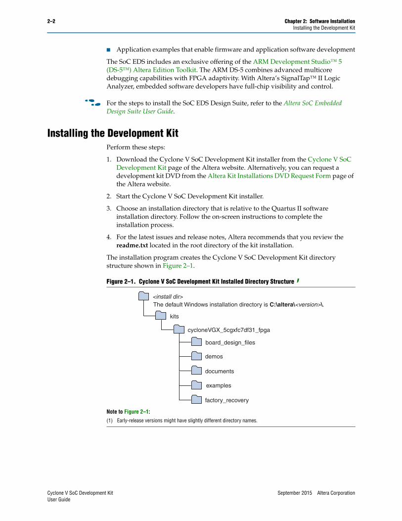
The installation program creates the Cyclone V SoC Development Kit directory structure shown in Figure 2–1.
Figure 2–1. Cyclone V SoC Development Kit Installed Directory Structure (1)
Note to Figure 2–1:
(1) Early-release versions might have slightly different directory names.
<install dir>
documents
board_design_files
The default Windows installation directory is C:\altera\<version>\.
examples
factory_recovery
demos
kits
cycloneVGX_5cgxfc7df31_fpga
Cyclone V SoC Development Kit September 2015 Altera CorporationUser Guide
Chapter 2: Software Installation 2–3Installing the USB-Blaster II Driver
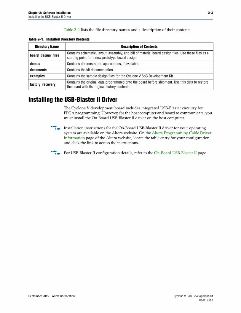
Table 2–1 lists the file directory names and a description of their contents.
Installing the USB-Blaster II DriverThe Cyclone V development board includes integrated USB-Blaster circuitry for FPGA programming. However, for the host computer and board to communicate, you must install the On-Board USB-Blaster II driver on the host computer.
f Installation instructions for the On-Board USB-Blaster II driver for your operating system are available on the Altera website. On the Altera Programming Cable Driver Information page of the Altera website, locate the table entry for your configuration and click the link to access the instructions.
f For USB-Blaster II configuration details, refer to the On-Board USB-Blaster II page.
Table 2–1. Installed Directory Contents
Directory Name Description of Contents
board_design_files Contains schematic, layout, assembly, and bill of material board design files. Use these files as a starting point for a new prototype board design.
demos Contains demonstration applications, if available.
documents Contains the kit documentation.
examples Contains the sample design files for the Cyclone V SoC Development Kit.
factory_recovery Contains the original data programmed onto the board before shipment. Use this data to restore the board with its original factory contents.
September 2015 Altera Corporation Cyclone V SoC Development KitUser Guide
2–4 Chapter 2: Software InstallationInstalling the USB-Blaster II Driver
Cyclone V SoC Development Kit September 2015 Altera CorporationUser Guide
September 2015 Altera Corporation
3. Development Board Setup
This chapter explains how to set up the Cyclone V SoC development board and restore default settings.
Setting Up the BoardTo prepare the board, perform these steps:
1. The development board ships with its board switches preconfigured to support the design examples in the kit. If you suspect your board might not be currently configured with the default settings, follow the instructions in “Factory Default Switch and Jumper Settings” on page 3–1 to return the board to its factory settings before proceeding.
The development board ships with the Golden System Reference Design binaries stored in the microSD card.
The microSD card also includes the following:
■ Hardware reference design FPGA image, Raw Binary File (.rbf) file
■ HPS image preloader U-Boot and Linux images
■ File system and software examples
2. Power up the development board by using the included laptop power supply plugged into J22 on the board.
c Use only the supplied power supply. Power regulation circuitry on the board can be damaged by power supplies with greater voltage, and a lower-rated power supply may not be able to provide enough power for the board.
Alternatively, you can use the an ATX power from a PC by plugging a 4-pin output from that supply to J20 on the development board.
c Make sure that the ATX supply is off when connecting to the board. Hot-swap is not supported and may damage the board's power supplies and other downstream devices.
When configuration is complete, the Config Done LED (D38) illuminates, signaling that the Cyclone V device configured successfully.
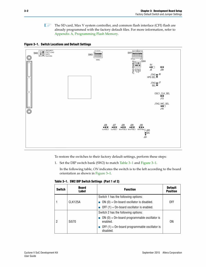
Factory Default Switch and Jumper SettingsThis section shows the factory settings (Figure 3–1) for the Cyclone V SoC development board. These settings ensure that the Board Update Portal and Golden System Reference design function properly.
Cyclone V SoC Development KitUser Guide
3–2 Chapter 3: Development Board SetupFactory Default Switch and Jumper Settings
1 The SD card, Max V system controller, and common flash interface (CFI) flash are already programmed with the factory default files. For more information, refer to Appendix A, Programming Flash Memory.
To restore the switches to their factory default settings, perform these steps:
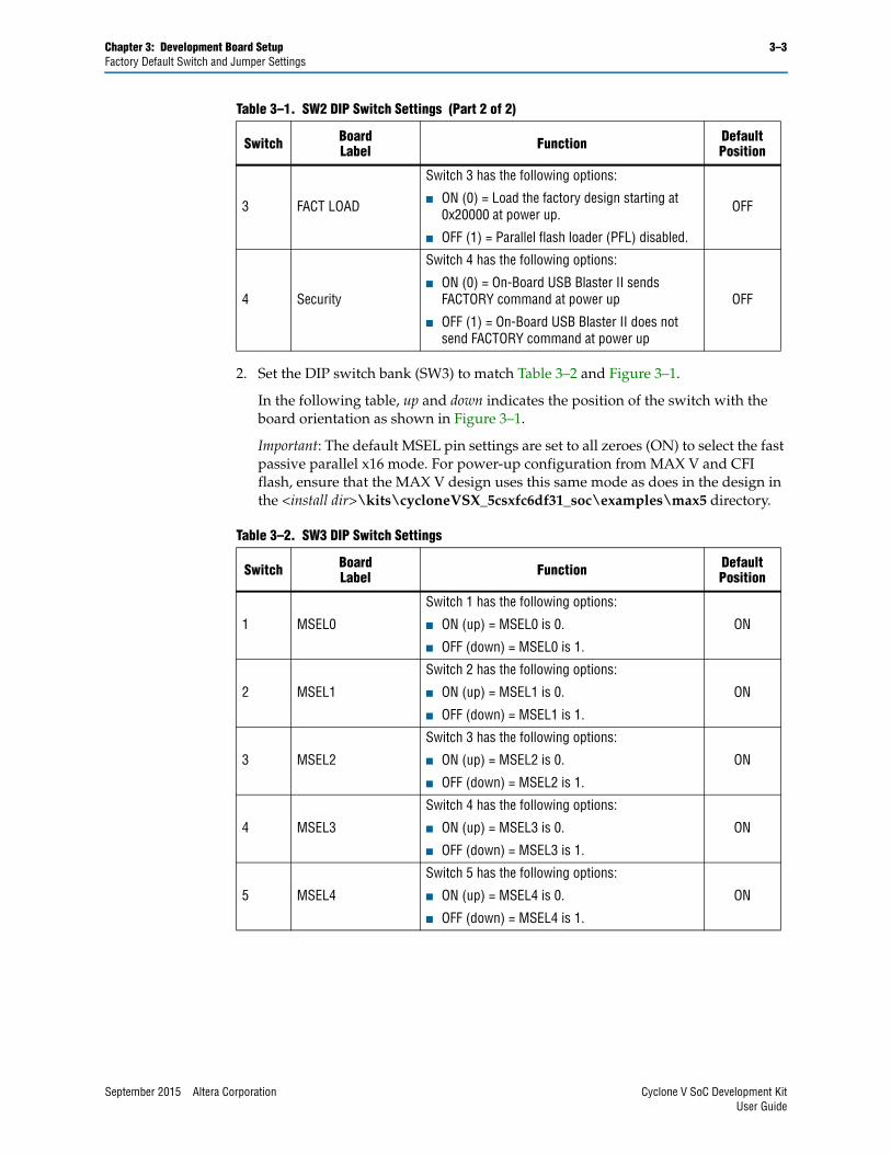
1. Set the DIP switch bank (SW2) to match Table 3–1 and Figure 3–1.
In the following table, ON indicates the switch is to the left according to the board orientation as shown in Figure 3–1.
Figure 3–1. Switch Locations and Default Settings
J5
9V
OSC1_CLK_SEL
J13
J16
J31
I2CSPI
J26 J27 J28 J29 J30
JTAG_MIC_SEL
J6JTAGHPS SEL
J7JTAGSEL
SW2SW31
2
3 4
SECURITYFACT LOADSi570CLK125A
0 1 2 3 4
MSEL
CLKSEL0 CLKSEL1 BOOTSEL0 BOOTSEL1 BOOTSEL2
HPS
FPG
AH
SMC
MAX
ON
ON
1 2 3 4 5 6
SW4
JTAG
ENA
BLE
1 2 3 4
ON
SW13 2 1 0 3 2 1 0
HPSFPGA
ON
1 2 3 4 5 6 7 8
J39
Table 3–1. SW2 DIP Switch Settings (Part 1 of 2)
Switch BoardLabel Function Default
Position
1 CLK125A
Switch 1 has the following options:
■ ON (0) = On-board oscillator is disabled.
■ OFF (1) = On-board oscillator is enabled.
OFF
2 Si570
Switch 2 has the following options:
■ ON (0) = On-board programmable oscillator is enabled.
■ OFF (1) = On-board programmable oscillator is disabled.
ON
Cyclone V SoC Development Kit September 2015 Altera CorporationUser Guide
Chapter 3: Development Board Setup 3–3Factory Default Switch and Jumper Settings
2. Set the DIP switch bank (SW3) to match Table 3–2 and Figure 3–1.
In the following table, up and down indicates the position of the switch with the board orientation as shown in Figure 3–1.
Important: The default MSEL pin settings are set to all zeroes (ON) to select the fast passive parallel x16 mode. For power-up configuration from MAX V and CFI flash, ensure that the MAX V design uses this same mode as does in the design in the <install dir>\kits\cycloneVSX_5csxfc6df31_soc\examples\max5 directory.
3 FACT LOAD
Switch 3 has the following options:
■ ON (0) = Load the factory design starting at 0x20000 at power up.
■ OFF (1) = Parallel flash loader (PFL) disabled.
OFF
4 Security
Switch 4 has the following options:
■ ON (0) = On-Board USB Blaster II sends FACTORY command at power up
■ OFF (1) = On-Board USB Blaster II does not send FACTORY command at power up
OFF
Table 3–2. SW3 DIP Switch Settings
Switch BoardLabel Function Default
Position
1 MSEL0
Switch 1 has the following options:
■ ON (up) = MSEL0 is 0.
■ OFF (down) = MSEL0 is 1.
ON
2 MSEL1
Switch 2 has the following options:
■ ON (up) = MSEL1 is 0.
■ OFF (down) = MSEL1 is 1.
ON
3 MSEL2
Switch 3 has the following options:
■ ON (up) = MSEL2 is 0.
■ OFF (down) = MSEL2 is 1.
ON
4 MSEL3
Switch 4 has the following options:
■ ON (up) = MSEL3 is 0.
■ OFF (down) = MSEL3 is 1.
ON
5 MSEL4
Switch 5 has the following options:
■ ON (up) = MSEL4 is 0.
■ OFF (down) = MSEL4 is 1.
ON
Table 3–1. SW2 DIP Switch Settings (Part 2 of 2)
Switch BoardLabel Function Default
Position
September 2015 Altera Corporation Cyclone V SoC Development KitUser Guide
3–4 Chapter 3: Development Board SetupFactory Default Switch and Jumper Settings
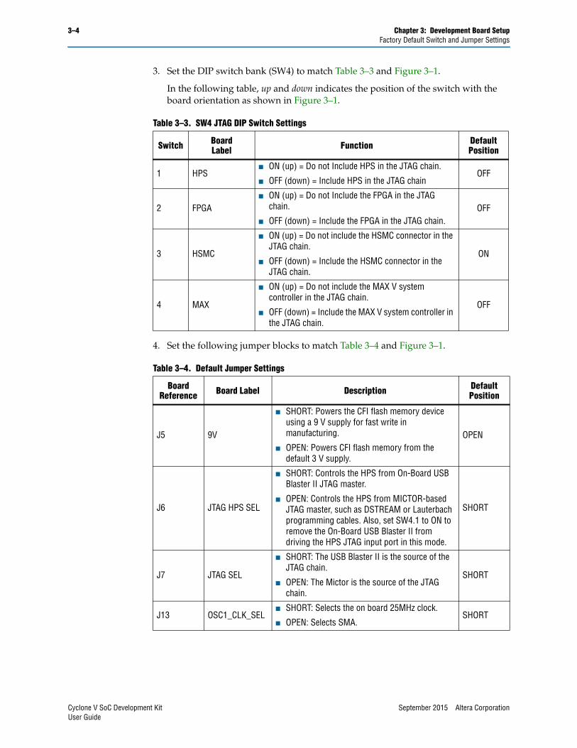
3. Set the DIP switch bank (SW4) to match Table 3–3 and Figure 3–1.
In the following table, up and down indicates the position of the switch with the board orientation as shown in Figure 3–1.
4. Set the following jumper blocks to match Table 3–4 and Figure 3–1.
Table 3–3. SW4 JTAG DIP Switch Settings
Switch BoardLabel Function Default
Position
1 HPS■ ON (up) = Do not Include HPS in the JTAG chain.
■ OFF (down) = Include HPS in the JTAG chainOFF
2 FPGA■ ON (up) = Do not Include the FPGA in the JTAG
chain.
■ OFF (down) = Include the FPGA in the JTAG chain.OFF
3 HSMC
■ ON (up) = Do not include the HSMC connector in the JTAG chain.
■ OFF (down) = Include the HSMC connector in the JTAG chain.
ON
4 MAX
■ ON (up) = Do not include the MAX V system controller in the JTAG chain.
■ OFF (down) = Include the MAX V system controller in the JTAG chain.
OFF
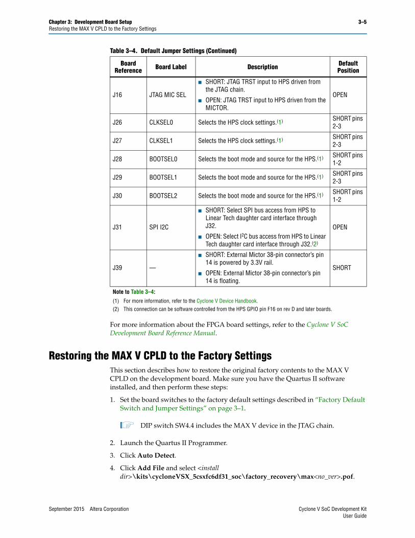
Table 3–4. Default Jumper Settings
Board Reference Board Label Description Default
Position
J5 9V
■ SHORT: Powers the CFI flash memory device using a 9 V supply for fast write in manufacturing.
■ OPEN: Powers CFI flash memory from the default 3 V supply.
OPEN
J6 JTAG HPS SEL
■ SHORT: Controls the HPS from On-Board USB Blaster II JTAG master.
■ OPEN: Controls the HPS from MICTOR-based JTAG master, such as DSTREAM or Lauterbach programming cables. Also, set SW4.1 to ON to remove the On-Board USB Blaster II from driving the HPS JTAG input port in this mode.
SHORT
J7 JTAG SEL
■ SHORT: The USB Blaster II is the source of the JTAG chain.
■ OPEN: The Mictor is the source of the JTAG chain.
SHORT
J13 OSC1_CLK_SEL■ SHORT: Selects the on board 25MHz clock.
■ OPEN: Selects SMA.SHORT
Cyclone V SoC Development Kit September 2015 Altera CorporationUser Guide
Chapter 3: Development Board Setup 3–5Restoring the MAX V CPLD to the Factory Settings
For more information about the FPGA board settings, refer to the Cyclone V SoC Development Board Reference Manual.
Restoring the MAX V CPLD to the Factory SettingsThis section describes how to restore the original factory contents to the MAX V CPLD on the development board. Make sure you have the Quartus II software installed, and then perform these steps:
1. Set the board switches to the factory default settings described in “Factory Default Switch and Jumper Settings” on page 3–1.
1 DIP switch SW4.4 includes the MAX V device in the JTAG chain.
2. Launch the Quartus II Programmer.
3. Click Auto Detect.
4. Click Add File and select <install dir>\kits\cycloneVSX_5csxfc6df31_soc\factory_recovery\max<no_ver>.pof.
J16 JTAG MIC SEL
■ SHORT: JTAG TRST input to HPS driven from the JTAG chain.
■ OPEN: JTAG TRST input to HPS driven from the MICTOR.
OPEN
J26 CLKSEL0 Selects the HPS clock settings.(1) SHORT pins 2-3
J27 CLKSEL1 Selects the HPS clock settings.(1) SHORT pins 2-3
J28 BOOTSEL0 Selects the boot mode and source for the HPS.(1) SHORT pins 1-2
J29 BOOTSEL1 Selects the boot mode and source for the HPS.(1) SHORT pins 2-3
J30 BOOTSEL2 Selects the boot mode and source for the HPS.(1) SHORT pins 1-2
J31 SPI I2C
■ SHORT: Select SPI bus access from HPS to Linear Tech daughter card interface through J32.
■ OPEN: Select I2C bus access from HPS to Linear Tech daughter card interface through J32.(2)
OPEN
J39 —
■ SHORT: External Mictor 38-pin connector’s pin 14 is powered by 3.3V rail.
■ OPEN: External Mictor 38-pin connector’s pin 14 is floating.
SHORT
Note to Table 3–4:
(1) For more information, refer to the Cyclone V Device Handbook.(2) This connection can be software controlled from the HPS GPIO pin F16 on rev D and later boards.
Table 3–4. Default Jumper Settings (Continued)
Board Reference Board Label Description Default
Position
September 2015 Altera Corporation Cyclone V SoC Development KitUser Guide
3–6 Chapter 3: Development Board SetupRestoring the CFI Flash Device to the Factory Defaults
5. Turn on the Program/Configure option for the added file.
6. Click Start to download the selected configuration file to the MAX V CPLD. Configuration is complete when the progress bar reaches 100%.
f To ensure that you have the most up-to-date factory restore files and product information, refer to the Cyclone V SoC Development Kit page of the Altera website.
Restoring the CFI Flash Device to the Factory DefaultsTo program the factory image to the flash device in the Quartus II Programmer, do the following steps:
1. On the Tools menu in the Quartus II software, click Programmer.
2. In the Programmer window, click Auto-Detect.
1 If you do not see USB Blaster or the board's embedded USB Blaster II listed next to Hardware Setup, refer to the “Installing the USB-Blaster II Driver” on page 2–3.
3. Click Add File and open <install dir>\kits\cycloneVSX_5csxfc6df31_soc\factory_recovery\max2_PFL_writer.pof.
4. Turn on the Program/Configure option for the .pof file.
5. Click Start to download the selected configuration file to the MAX V CPLD. Configuration is complete when the progress bar reaches 100%
6. Click Auto Detect and a flash device should show up attached to the MAX V in the main window.
7. Double-click the graphic of the flash device in the device chain pane to display the Device’s Properties dialog box.
8. Select the flash image .pof file: <install dir>\kits\cycloneVSX_5csxfc6df31_soc\factory_recovery\output_file.pof.
9. Once the flash image .pof is attached in the Quartus II Programmer, turn on Page_1 and Option Bits. (Page_0 is reserved for the GSRD factory design.)
10. Click Start.
11. After the flash writing process has completed, power cycle the board and look for the MAX CONF DONE LED to turn ON if successful.
12. Altera recommends that you return to the Max V System Controller factory design after completing the flash writing. To do so, program the Max V with <install dir>\kits\cycloneVSX_5csxfc6df31_soc\factory_recovery\max<version>.pof. For more information, refer to “Restoring the MAX V CPLD to the Factory Settings” on page 3–5.
1 The flash writer version blinks the SEL 2, 1, and 0 LEDs and does not support the Power Monitor, Clock Control, or other logic functions. Use the flash writer only for flash programming.
Cyclone V SoC Development Kit September 2015 Altera CorporationUser Guide
Chapter 3: Development Board Setup 3–7Restoring the CFI Flash Device to the Factory Defaults
f To ensure that you have the most up-to-date factory restore files and information about this product, refer to the Cyclone V SoC Development Kit page of the Altera website.
September 2015 Altera Corporation Cyclone V SoC Development KitUser Guide
3–8 Chapter 3: Development Board SetupRestoring the CFI Flash Device to the Factory Defaults
Cyclone V SoC Development Kit September 2015 Altera CorporationUser Guide
September 2015 Altera Corporation
4. Board Update Portal
The Board Update Portal web page provides links to useful information on the Altera website. You can use this web page to interact with your board:
■ Blinking LEDs
■ Writing text messages to the LCD
■ Mouse over the board photo to view features
The Board Update Portal web page is served by the web server application running on the HPS on your board.
Connecting to the Board Update Portal Web PageEnsure that you have the following setup or installed:
■ A PC with a connection to a working Ethernet port on a DHCP enabled network.
■ A separate working Ethernet port connected to the same network for the board.
■ The Ethernet and power cables that are included in the kit.
To connect to the Board Update Portal web page, perform these steps:
1. Ensure that the CSEL and BSEL jumpers (Table 3–4 on page 3–4) and the DIP switch SW2.3 (Table 3–1 on page 3–2) are in the factory default positions.
2. Attach an Ethernet cable to the HPS Ethernet connector (J2) on the upper left of the board to your LAN.
3. Power up the board. The board connects to the LAN’s gateway router and obtains an IP address and displays it to the LCD. If no IP address is obtained, the LCD displays No IP obtained. If the system booted, the LCD displays Hello Tim.
If the LCD displays No IP obtained, your system partially booted, but without Ethernet access. If you receive the No IP obtained message, Altera recommends that you install the USB virtual COM port drivers to access the Linux system through a terminal window.
f For more information, refer to the Configuring Serial Connection section of the Linux Getting Started page on RocketBoards.org.
1 There are several reasons why your board may fail to get and IP address in this step:
■ Your port is not active or the cable is not plugged in.
■ You do not have a DHCP server.
■ Your DHCP server ran out of addresses.
■ Your DHCP server was not allowed to respond to the board due to security filters, such as MAC address filtering.
Cyclone V SoC Development KitUser Guide
4–2 Chapter 4: Board Update PortalConnecting to the Board Update Portal Web Page
4. Launch a web browser on a PC that is connected to the same network, and enter the IP address from the LCD into the browser address bar. The Board Update Portal web page appears in the browser.
1 You can click Cyclone V SoC Development Kit on the Board Update Portal web page to access the kit’s home page for documentation updates and additional new designs.
f You can also navigate directly to the Cyclone V SoC Development Kit page of the Altera website to determine if you have the latest kit software.
Cyclone V SoC Development Kit September 2015 Altera CorporationUser Guide
September 2015 Altera Corporation
5. Board Test System
The development kit includes an application called the Board Test System (BTS) and related design examples. The BTS provides an easy-to-use interface to alter functional settings and observe the results. You can use the BTS to test board components, modify functional parameters, observe performance, and measure power usage. (While using the BTS, you reconfigure the FPGA several times with test designs specific to the functionality you are testing.)
To install the BTS, follow the steps in “Installing the Development Kit” on page 2–2.
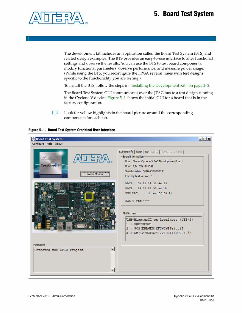
The Board Test System GUI communicates over the JTAG bus to a test design running in the Cyclone V device. Figure 5–1 shows the initial GUI for a board that is in the factory configuration.
1 Look for yellow highlights in the board picture around the corresponding components for each tab.
Figure 5–1. Board Test System Graphical User Interface
Cyclone V SoC Development KitUser Guide
5–2 Chapter 5: Board Test SystemPreparing the Board for the Board Test System
Several designs are provided to test the major board features. Each design provides data for one or more tabs in the application. The Configure menu identifies the appropriate design to download to the FPGA for each tab.
After successful FPGA configuration, the appropriate tab appears that allows you to exercise the related board features.
The Power Monitor button starts the Power Monitor application that measures and reports current power information for the board. Because the application communicates over the JTAG bus to the MAX II device, you can measure the power of any design in the FPGA, including your own designs.
1 The Board Test System and Power Monitor share the JTAG bus with other applications like the Nios II debugger and the SignalTap® II Embedded Logic Analyzer. Because the Quartus II programmer uses most of the bandwidth of the JTAG bus, other applications using the JTAG bus might time out. Be sure to close the other applications before attempting to reconfigure the FPGA using the Quartus II Programmer.
Preparing the Board for the Board Test SystemWith the power to the board off, follow these steps:
1. Plug the included USB cable from J37 (USB-Blaster II interface) to the host computer’s USB port.
2. Ensure that the development board switches and jumpers are set to the default positions as shown in the “Factory Default Switch and Jumper Settings” section starting on page 3–1.
f For more information about the board’s DIP switch and jumper settings, refer to the Cyclone V SoC Development Board Reference Manual.
c To ensure operating stability, keep the USB cable connected and the board powered on when running the demonstration application. The application cannot run correctly unless the USB cable is attached and the board is on.
Running the Board Test SystemNavigate to the <install dir>\kits\cycloneVSX_5csxfc6df31_soc\examples\board_test_system directory and run the BoardTestSystem.exe application.
1 To run the BTS in Windows, you can also click Start > All Programs > Altera > Cyclone V SoC Development Kit <version> > Board Test System.
A GUI appears, displaying the application tab that corresponds to the design running in the FPGA. Typically the board will not be pre-programmed with a BTS design. One must be loaded using the Configure menu as described in the next section.
Cyclone V SoC Development Kit September 2015 Altera CorporationUser Guide
Chapter 5: Board Test System 5–3Using the Board Test System
Using the Board Test SystemThis section describes each control in the BTS.
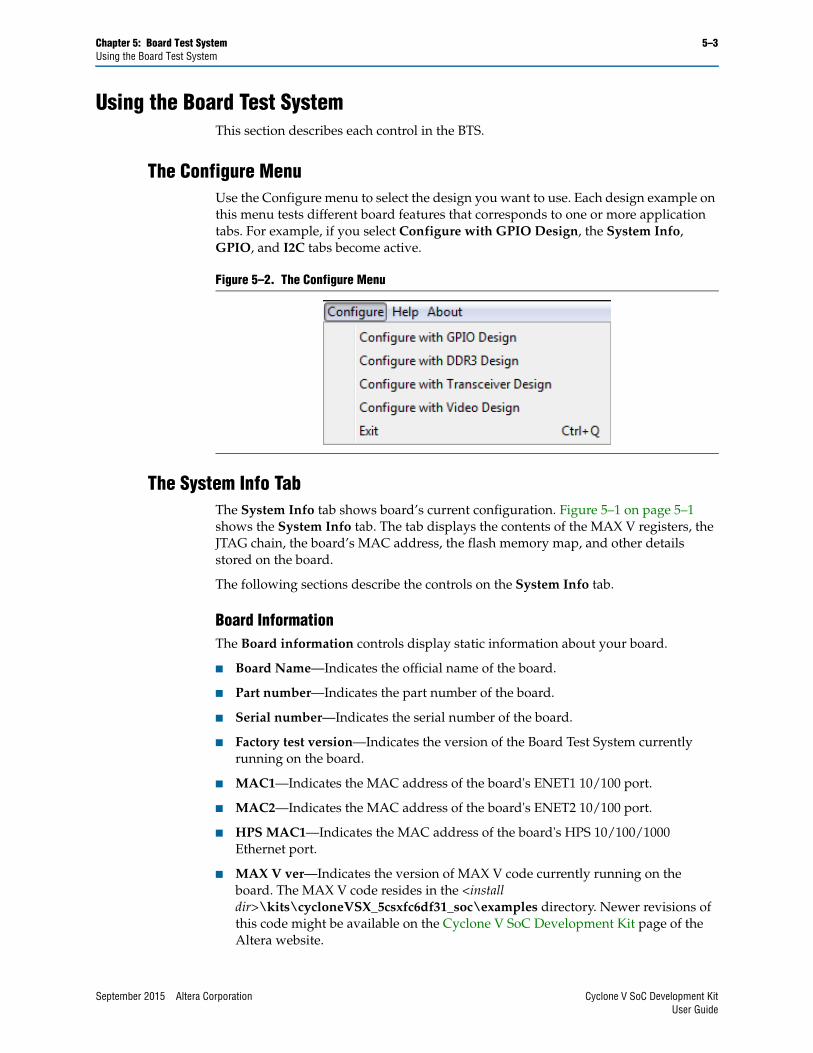
The Configure MenuUse the Configure menu to select the design you want to use. Each design example on this menu tests different board features that corresponds to one or more application tabs. For example, if you select Configure with GPIO Design, the System Info, GPIO, and I2C tabs become active.
The System Info TabThe System Info tab shows board’s current configuration. Figure 5–1 on page 5–1 shows the System Info tab. The tab displays the contents of the MAX V registers, the JTAG chain, the board’s MAC address, the flash memory map, and other details stored on the board.
The following sections describe the controls on the System Info tab.
Board InformationThe Board information controls display static information about your board.
■ Board Name—Indicates the official name of the board.
■ Part number—Indicates the part number of the board.
■ Serial number—Indicates the serial number of the board.
■ Factory test version—Indicates the version of the Board Test System currently running on the board.
■ MAC1—Indicates the MAC address of the board's ENET1 10/100 port.
■ MAC2—Indicates the MAC address of the board's ENET2 10/100 port.
■ HPS MAC1—Indicates the MAC address of the board's HPS 10/100/1000 Ethernet port.
■ MAX V ver—Indicates the version of MAX V code currently running on the board. The MAX V code resides in the <install dir>\kits\cycloneVSX_5csxfc6df31_soc\examples directory. Newer revisions of this code might be available on the Cyclone V SoC Development Kit page of the Altera website.
Figure 5–2. The Configure Menu
September 2015 Altera Corporation Cyclone V SoC Development KitUser Guide
5–4 Chapter 5: Board Test SystemUsing the Board Test System
JTAG ChainThe JTAG chain control shows all the devices currently in the JTAG chain. The Cyclone V device is always the first device in the chain. The JTAG chain is normally mastered by the On-board USB-Blaster II.
1 If you plug in an external USB-Blaster cable to the JTAG header (J23), the On-Board USB-Blaster II is disabled.
1 JTAG DIP switch bank (SW4) selects which interfaces are in the chain. Refer to Table 3–3 on page 3–4 for detailed settings.
f For details on the JTAG chain, refer to the Cyclone V SoC Development Board Reference Manual. For USB-Blaster II configuration details, refer to the On-Board USB-Blaster II page.
Cyclone V SoC Development Kit September 2015 Altera CorporationUser Guide
Chapter 5: Board Test System 5–5Using the Board Test System
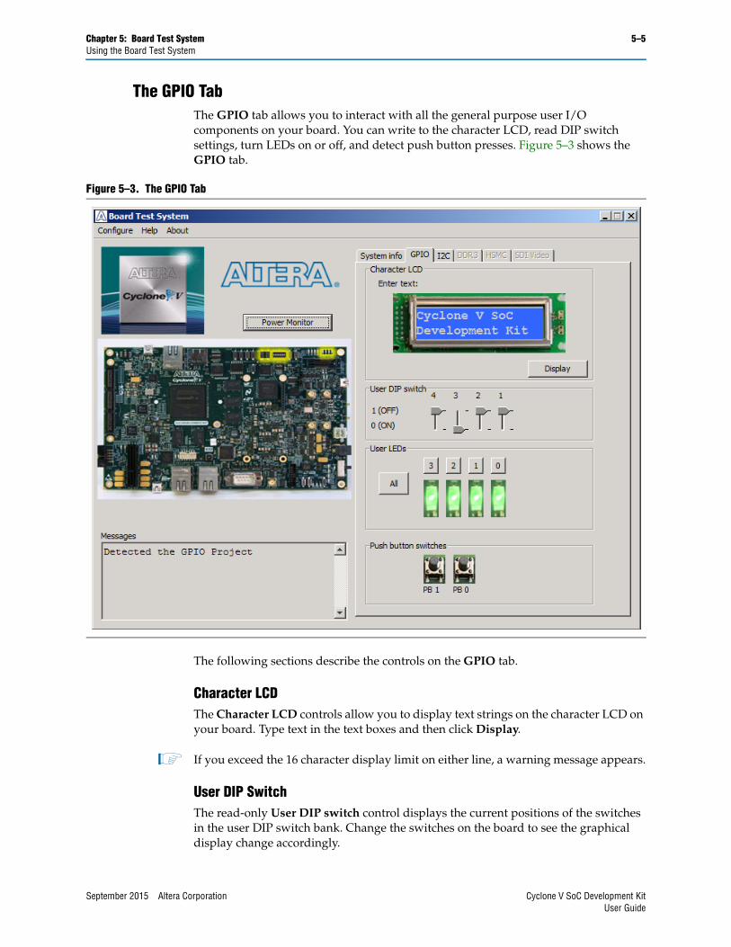
The GPIO TabThe GPIO tab allows you to interact with all the general purpose user I/O components on your board. You can write to the character LCD, read DIP switch settings, turn LEDs on or off, and detect push button presses. Figure 5–3 shows the GPIO tab.
The following sections describe the controls on the GPIO tab.
Character LCDThe Character LCD controls allow you to display text strings on the character LCD on your board. Type text in the text boxes and then click Display.
1 If you exceed the 16 character display limit on either line, a warning message appears.
User DIP SwitchThe read-only User DIP switch control displays the current positions of the switches in the user DIP switch bank. Change the switches on the board to see the graphical display change accordingly.
Figure 5–3. The GPIO Tab
September 2015 Altera Corporation Cyclone V SoC Development KitUser Guide
5–6 Chapter 5: Board Test SystemUsing the Board Test System
User LEDsThe User LEDs control displays the current state of the user LEDs. Click the graphical representation of the LEDs to turn the board LEDs on and off. You can click ALL to turn on and off all of the user LEDs at once.
Push Button SwitchesThe read-only Push Button switches control displays the current state of the board user push buttons. Press a push button on the board to see the graphical display change accordingly.
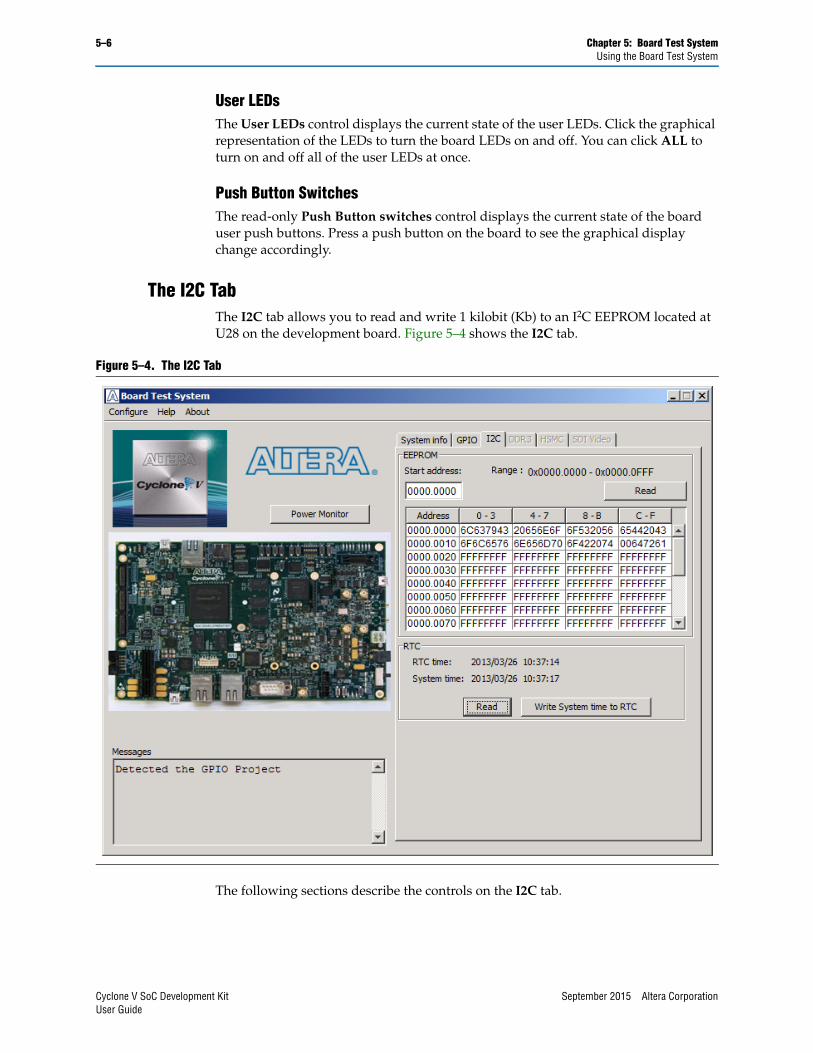
The I2C TabThe I2C tab allows you to read and write 1 kilobit (Kb) to an I2C EEPROM located at U28 on the development board. Figure 5–4 shows the I2C tab.
The following sections describe the controls on the I2C tab.
Figure 5–4. The I2C Tab
Cyclone V SoC Development Kit September 2015 Altera CorporationUser Guide
Chapter 5: Board Test System 5–7Using the Board Test System
EEPROMThe serial I2C EEPROM is 32 Kilobits.
■ Start Address—0x0
■ Range—0x1000
■ Read—Reads data from the I2C EEPROM.
f For more information on the EEPROM, refer to the Cyclone V SoC Development Board Reference Manual.
RTCReal time clock.
■ Current Time—Displays current time stored in RTC memory when you click Read. It is not updated automatically.
■ System Time—Displays current time from PC and is updated automatically.
■ Read—Reads the time from the RTC device on the board.
■ Write System Time to RTC—Writes the time to the RTC device on the board.
September 2015 Altera Corporation Cyclone V SoC Development KitUser Guide
5–8 Chapter 5: Board Test SystemUsing the Board Test System
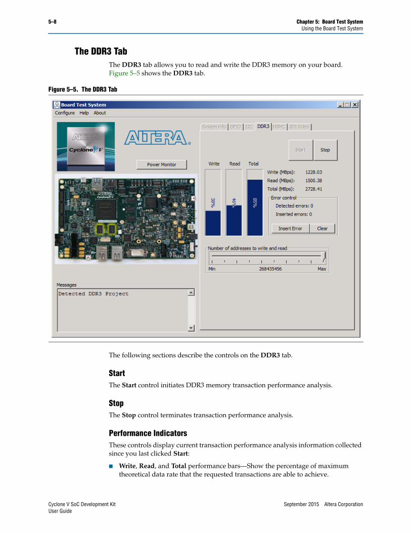
The DDR3 TabThe DDR3 tab allows you to read and write the DDR3 memory on your board. Figure 5–5 shows the DDR3 tab.
The following sections describe the controls on the DDR3 tab.
StartThe Start control initiates DDR3 memory transaction performance analysis.
StopThe Stop control terminates transaction performance analysis.
Performance IndicatorsThese controls display current transaction performance analysis information collected since you last clicked Start:
■ Write, Read, and Total performance bars—Show the percentage of maximum theoretical data rate that the requested transactions are able to achieve.
Figure 5–5. The DDR3 Tab
Cyclone V SoC Development Kit September 2015 Altera CorporationUser Guide
Chapter 5: Board Test System 5–9Using the Board Test System
■ Write (MBps), Read (MBps), and Total (MBps)—Show the number of bytes of data analyzed per second. The data bus is 72 bits wide and the frequency is 400 MHz double data rate (800 Mbps per pin), equating to a theoretical maximum bandwidth of 3200 Megabits per second or 400 MBps.
Error ControlThe Error control control displays data errors detected during analysis and allows you to insert errors:
■ Detected errors—Displays the number of data errors detected in the hardware.
■ Inserted errors—Displays the number of errors inserted into the transaction stream.
■ Insert Error—Inserts a one-word error into the transaction stream each time you click the button. Insert Error is only enabled during transaction performance analysis.
■ Clear—Resets the Detected errors and Inserted errors counters to zeros.
Number of Addresses to Write and ReadThe Number of addresses to write and read control determines the number of addresses to use in each iteration of reads and writes.
September 2015 Altera Corporation Cyclone V SoC Development KitUser Guide
5–10 Chapter 5: Board Test SystemUsing the Board Test System
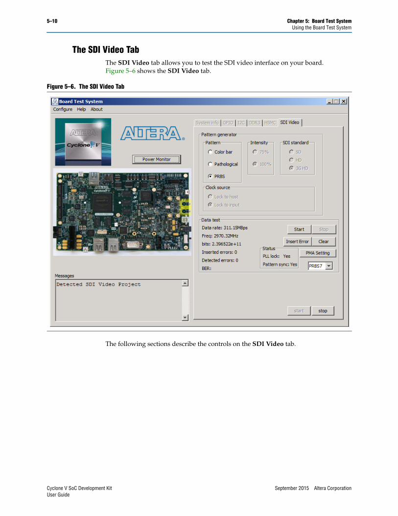
The SDI Video TabThe SDI Video tab allows you to test the SDI video interface on your board. Figure 5–6 shows the SDI Video tab.
The following sections describe the controls on the SDI Video tab.
Figure 5–6. The SDI Video Tab
Cyclone V SoC Development Kit September 2015 Altera CorporationUser Guide
Chapter 5: Board Test System 5–11Using the Board Test System
Pattern GeneratorThis control specifies the test pattern to output to the monitor. The following choices are available:
Pattern
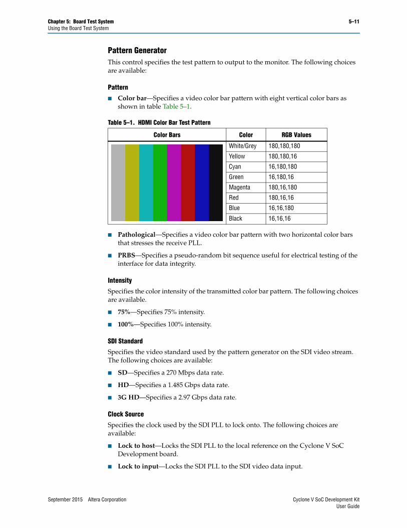
■ Color bar—Specifies a video color bar pattern with eight vertical color bars as shown in table Table 5–1.
■ Pathological—Specifies a video color bar pattern with two horizontal color bars that stresses the receive PLL.
■ PRBS—Specifies a pseudo-random bit sequence useful for electrical testing of the interface for data integrity.
Intensity
Specifies the color intensity of the transmitted color bar pattern. The following choices are available.
■ 75%—Specifies 75% intensity.
■ 100%—Specifies 100% intensity.
SDI Standard
Specifies the video standard used by the pattern generator on the SDI video stream. The following choices are available:
■ SD—Specifies a 270 Mbps data rate.
■ HD—Specifies a 1.485 Gbps data rate.
■ 3G HD—Specifies a 2.97 Gbps data rate.
Clock Source
Specifies the clock used by the SDI PLL to lock onto. The following choices are available:
■ Lock to host—Locks the SDI PLL to the local reference on the Cyclone V SoC Development board.
■ Lock to input—Locks the SDI PLL to the SDI video data input.
Table 5–1. HDMI Color Bar Test Pattern
Color Bars Color RGB Values
White/Grey 180,180,180
Yellow 180,180,16
Cyan 16,180,180
Green 16,180,16
Magenta 180,16,180
Red 180,16,16
Blue 16,16,180
Black 16,16,16
September 2015 Altera Corporation Cyclone V SoC Development KitUser Guide
5–12 Chapter 5: Board Test SystemUsing the Board Test System
Data Test
This group displays information about the SDI interface test when running in PRBS mode in the patter generator.
■ Data rate—Displays the current SDI data rate in megabytes per second (MBps).
■ Freq—Displays the data rate frequency in MHz which is equivalent to Mbps.
■ Bits—Displays the number of bits transmitted since clicking Start.
■ Inserted errors—Displays the number of errors inserted by clicking Insert Error button.
■ Detected errors—Displays the number of bit errors detected by the error checking circuitry.
■ BER—Displays the bit error rate of the interface.
■ PLL lock—Displays Yes if the SDI PLL is locked.
■ Pattern Sync—Displays Yes if the receiver has detected the input data pattern.
■ Start— Starts the PRBS data test and begins to monitor and update screen with live test results.
■ Stop—Stops the PRBS data test.
■ Insert Error—Inserts an error into an SDI data stream that is detected by the receiver when in loopback using the included video cable.
■ Clear—Clears the Detected errors counter.
■ PMA Setting—Opens the PMA settings window that allows for adjusting the analog transceiver settings, such as output voltage, loopback settings, and equalization.
■ PRBS (list)—Selects the transmit pattern and sets the receive error detection circuitry to expect the same pattern for use in loopback testing.
Cyclone V SoC Development Kit September 2015 Altera CorporationUser Guide
Chapter 5: Board Test System 5–13Using the Board Test System
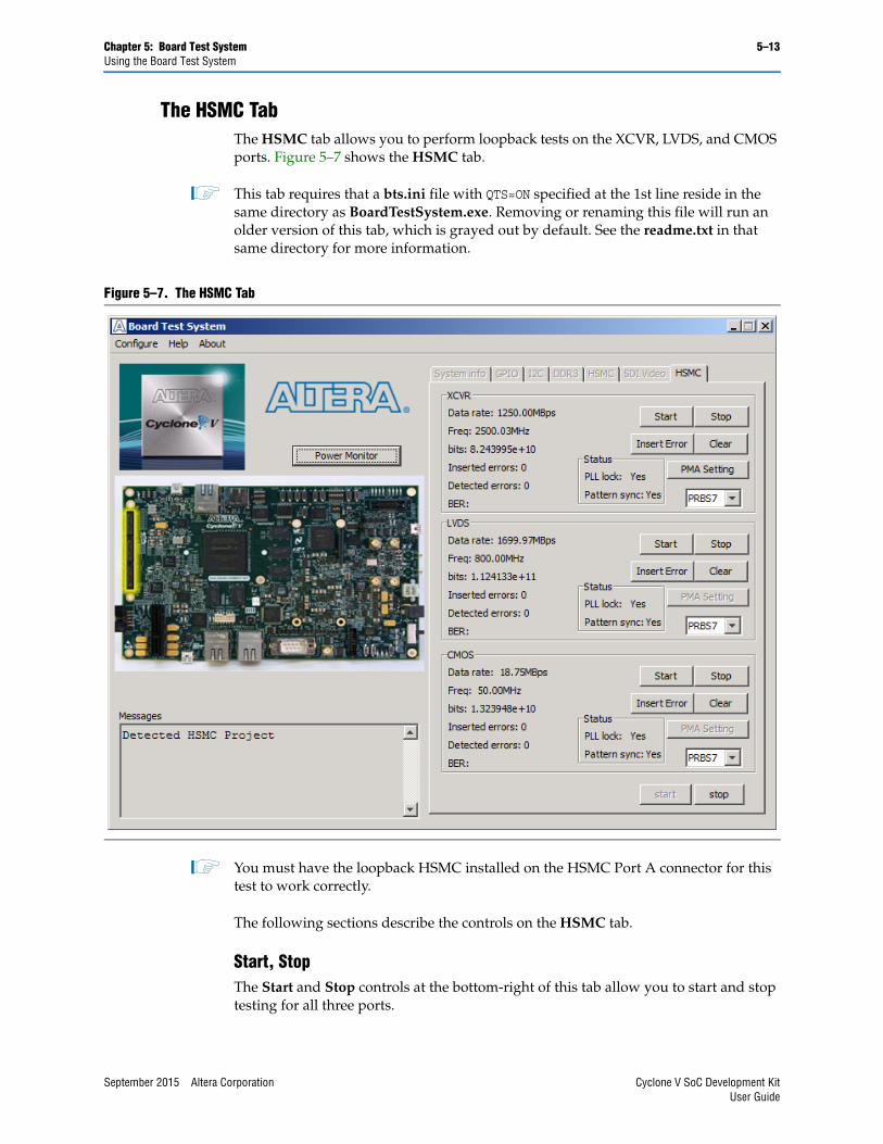
The HSMC TabThe HSMC tab allows you to perform loopback tests on the XCVR, LVDS, and CMOS ports. Figure 5–7 shows the HSMC tab.
1 This tab requires that a bts.ini file with QTS=ON specified at the 1st line reside in the same directory as BoardTestSystem.exe. Removing or renaming this file will run an older version of this tab, which is grayed out by default. See the readme.txt in that same directory for more information.
1 You must have the loopback HSMC installed on the HSMC Port A connector for this test to work correctly.
The following sections describe the controls on the HSMC tab.
Start, StopThe Start and Stop controls at the bottom-right of this tab allow you to start and stop testing for all three ports.
Figure 5–7. The HSMC Tab
September 2015 Altera Corporation Cyclone V SoC Development KitUser Guide
5–14 Chapter 5: Board Test SystemUsing the Board Test System
XCVR, LVDS, CMOSThese groups displays the following XCVR, LVDS, CMOS status information during the loopback test:
■ Data rate—Displays the current XCVR data rate in megabytes per second (MBps).
■ Freq—Displays the data rate frequency in MHz which is equivalent to Mbps.
■ Bits—Displays the number of bits transmitted since clicking Start.
■ Inserted errors—Displays the number of errors inserted by clicking Insert Error button.
■ Detected errors—Displays the number of bit errors detected by the error checking circuitry.
■ BER—Displays the bit error rate of the interface.
■ PLL lock—Displays Yes if the SDI PLL is locked.
■ Pattern Sync—Displays Yes if the receiver has detected the input data pattern.
■ Start— Starts the PRBS data test and begins to monitor and update screen with live test results.
■ Stop—Stops the PRBS data test.
■ Insert Error—Inserts an error into a data stream that is detected by the receiver when in loopback using the included video cable.
With the Insert Error, there are differences among the three ports:
XCVR—inserts 4 errors at 1 click due to 4 test control blocks in the design.
LVDS—inserts 3 errors at 1 click due to 3 test control block in the design.
CMOS—inserts 1 error at 1 click.
■ Clear—Clears the Detected errors counter.
■ PMA Setting—Opens the PMA settings window that allows for adjusting the analog transceiver settings, such as output voltage, loopback settings, and equalization.
The following settings are available for analysis:
■ Serial Loopback—Routes the selected TX output signal back to the RX input signal on-chip to verify operation without using an external loopback board.
■ VOD—Specifies the voltage output (differential) of the transmitter buffer.
■ Pre-emphasis tap
■ Pre—Specifies the amount of pre-emphasis on the pre-tap of the transmitter buffer.
■ First post—Specifies the amount of pre-emphasis on the first post tap of the transmitter buffer.
■ Second post—Specifies the amount of pre-emphasis on the second post tap of the transmitter buffer.
Cyclone V SoC Development Kit September 2015 Altera CorporationUser Guide
Chapter 5: Board Test System 5–15The Power Monitor
1 Support for this tap is device and software version dependent.
■ Equalizer—Specifies the setting for the receiver equalizer.
■ DC gain—Specifies the DC portion of the receiver equalizer.
■ PRBS—Selects the transmit pattern and sets the receive error detection circuitry to expect the same pattern for use in loopback testing.
The Power MonitorThe Power Monitor measures and reports current power information. To start the application, click Power Monitor in the Board Test System application.
1 You can also run the Power Monitor as a stand-alone application. PowerMonitor.exe resides in the <install dir>\kits\cycloneVSX_5csxfc6df31_soc\examples\board_test_system directory.
In Windows, click Start > All Programs > Altera > Cyclone V SoC Development Kit <version> > Power Monitor to start the application.
The Power Monitor communicates with the MAX V device on the board through the JTAG bus. A power monitor circuit attached to the MAX V device allows you to measure the power that the Cyclone V FPGA is consuming.
1 The Power Monitor measures power over an I2C bus with multiple masters. You might see some glitches in the measurements if the HPS is booted. The GSRD and other Linux images access the I2C bus periodically and cause inaccurate measurements for a cycle or two. These should go away and likely return to an accurate, steady state measurement for most designs.
September 2015 Altera Corporation Cyclone V SoC Development KitUser Guide
5–16 Chapter 5: Board Test SystemThe Power Monitor
Figure 5–8 shows the Power Monitor.
The following sections describe the Power Monitor controls.
U34 and U26The U34 and U26 groups show the power rail graphs. They display the mA power consumption of your board over time.
The green line indicates the current value. The red line indicates the maximum value read since the last reset.
1 You can enlarge a graph by clicking on it. Click it again to restore the original size.
Temp on 2978
The temperature controls display only the temperature from the power supply manager, not the FPGA.
Total Power
These controls display the sum of all four rails for each group, U34 and for U26.
ControlsThis group contains the following controls:
■ Start—Starts the communication with the board to monitor power.
Figure 5–8. The Power Monitor
Cyclone V SoC Development Kit September 2015 Altera CorporationUser Guide
Chapter 5: Board Test System 5–17The Clock Control
■ Stop—Stops the communication with the board to monitor power.
■ Update speed—Specifies how often to refresh the graph.
■ Log Results—Specifies that a log file is saved to <install dir>\kits\cycloneVSX_5csxfc6df31_soc\examples\board_test_system.
■ MAX V version—Indicates the version of MAX V code currently running on the board. The MAX V code resides in the <install dir>\kits\cycloneVSX_5csxfc6df31_soc\factory_recovery and <install dir>\kits\cycloneVSX_5csxfc6df31_soc\examples\max5 directories.
1 Newer revisions of this code might be available on the Cyclone V SoC Development Kit page of the Altera website.
f A table with the power rail information is available in the Cyclone V SoC Development Board Reference Manual.
The Clock ControlThe Clock Control application sets the Si570 (X1) or Si571 (X3) programmable oscillators to any frequency between 10 MHz and 810 MHz. The frequencies support eight digits of precision to the right of the decimal point.
The Clock Control application runs as a stand-alone application. ClockControl.exe resides in the <install dir>\kits\cycloneVSX_5csxfc6df31_soc\examples\board_test_system directory.
To start the application, click Start > All Programs > Altera > Cyclone V SoC Development Kit <version> > Clock Control.
f For more information about the Si570/Si571 and the Cyclone V development board’s clocking circuitry and clock input pins, refer to the Cyclone V SoC Development Board Reference Manual.
September 2015 Altera Corporation Cyclone V SoC Development KitUser Guide
5–18 Chapter 5: Board Test SystemThe Clock Control
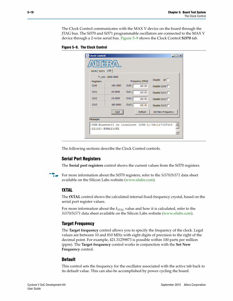
The Clock Control communicates with the MAX V device on the board through the JTAG bus. The Si570 and Si571 programmable oscillators are connected to the MAX V device through a 2-wire serial bus. Figure 5–9 shows the Clock Control Si570 tab.
The following sections describe the Clock Control controls.
Serial Port RegistersThe Serial port registers control shows the current values from the Si570 registers.
f For more information about the Si570 registers, refer to the Si570/Si571 data sheet available on the Silicon Labs website (www.silabs.com).
fXTALThe fXTAL control shows the calculated internal fixed-frequency crystal, based on the serial port register values.
For more information about the fXTAL value and how it is calculated, refer to the Si570/Si571 data sheet available on the Silicon Labs website (www.silabs.com).
Target FrequencyThe Target frequency control allows you to specify the frequency of the clock. Legal values are between 10 and 810 MHz with eight digits of precision to the right of the decimal point. For example, 421.31259873 is possible within 100 parts per million (ppm). The Target frequency control works in conjunction with the Set New Frequency control.
DefaultThis control sets the frequency for the oscillator associated with the active tab back to its default value. This can also be accomplished by power cycling the board.
Figure 5–9. The Clock Control
Cyclone V SoC Development Kit September 2015 Altera CorporationUser Guide
Chapter 5: Board Test System 5–19Configuring the FPGA Using the Quartus II Programmer
Set New FrequencyThe Set New Frequency control sets the programmable oscillator frequency for the selected clock to the value in the Target frequency control for the Si570 (X1) and Si571 (X3). Frequency changes might take several milliseconds to take effect. You might see glitches on the clock during this time. Altera recommends resetting the FPGA logic after changing frequencies.
Configuring the FPGA Using the Quartus II ProgrammerYou can use the Quartus II Programmer to configure the FPGA with your SRAM Object File (.sof) file.
Before ConfiguringEnsure the following:
■ The Quartus II Programmer and the USB-Blaster II driver are installed on the host computer.
■ The USB cable is connected to the development board.
■ Power to the board is on, and no other applications that use the JTAG chain are running.
If the Quartus II Programmer window is already open, and you power cycle the board, to detect the JTAG chain, do the following:
■ Click Hardware Setup in the Quartus II Programmer window.
■ Reselect USB-Blaster II in order to properly detect the JTAG chain.
Configuring the FPGAPerform these steps:
1. Start the Quartus II Programmer.
2. Click Auto Detect to display the devices in the JTAG chain.
3. Click Add File and select the path to the desired .sof.
4. Turn on the Program/Configure option for the added file.
5. Click Start to download the selected file to the FPGA. Configuration is complete when the progress bar reaches 100%.
1 Using the Quartus II Programmer to configure a device on the board causes other JTAG-based applications such as the Board Test System and the Power Monitor to lose their connection to the board. Restart those applications after configuration is complete.
September 2015 Altera Corporation Cyclone V SoC Development KitUser Guide

5–20 Chapter 5: Board Test SystemConfiguring the FPGA Using the Quartus II Programmer
Cyclone V SoC Development Kit September 2015 Altera CorporationUser Guide
September 2015 Altera Corporation
A. Programming Flash Memory
This appendix describes programming information for the following memory devices:
■ Common flash interface (CFI) flash memory
■ Quad serial peripheral interface (quad SPI) flash memory
■ SD card flash memory
The Cyclone V development board’s flash memory ships preconfigured with the parallel flash loader (PFL) option bits to support FPGA designs to be written to any of the three locations as shown in Table A–1. The PFL is disabled by default. Set SW2.3 to ON to enable FPGA programming from CFI flash memory on power up.
1 There are several other factory software files written to flash memory to support the Board Update Portal. These software files were created using the Nios II EDS, just as the hardware design was created using the Quartus II software.
CFI Flash Memory
CFI Flash Memory MapTable A–1 shows the default memory contents of the 512 Mb CFI flash device.
c Altera recommends that you do not overwrite the factory hardware images unless you are an expert with Altera tools. If you unintentionally overwrite the factory hardware or factory software image, refer to “Restoring the CFI Flash Device to the Factory Defaults” on page 3–6.
Programming CFI Flash Using the Quartus II ProgrammerYou can use the JTAG interface in Altera CPLDs to indirectly program the flash memory device. The Altera CPLD JTAG block interfaces directly with the logic array in a special JTAG mode. This mode brings the JTAG chain through the logic array instead of the Altera CPLD boundary-scan cells (BSC). The PFL megafunction provides JTAG interface logic to do the following:
■ Convert the JTAG stream provided by the Quartus II software.
Table A–1. Byte Address Flash Memory Map
Block Description KB Size Address Range
Unused 44711 0x0145.635C - 03FF.FFFF
User hardware 2 6872 0x00DA.0000 - 0145.635B
User hardware 1 6872 0x006E.0000 - 00D9.635B
Factory hardware 6872 0x0002.0000 - 006D.635B
PFL option bits 32 0x0001.8000 - 0001.8080
Cyclone V SoC Development KitUser Guide
A–2 Appendix A: Programming Flash MemoryCFI Flash Memory
■ Program the CFI flash memory devices connected to the CPLD I/O pins.
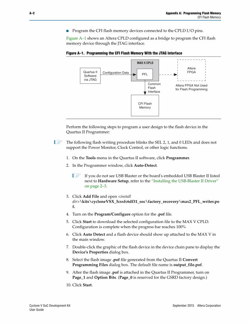
Figure A–1 shows an Altera CPLD configured as a bridge to program the CFI flash memory device through the JTAG interface.
Perform the following steps to program a user design to the flash device in the Quartus II Programmer:
1 The following flash writing procedure blinks the SEL 2, 1, and 0 LEDs and does not support the Power Monitor, Clock Control, or other logic functions.
1. On the Tools menu in the Quartus II software, click Programmer.
2. In the Programmer window, click Auto-Detect.
1 If you do not see USB Blaster or the board's embedded USB Blaster II listed next to Hardware Setup, refer to the “Installing the USB-Blaster II Driver” on page 2–3.
3. Click Add File and open <install dir>\kits\cycloneVSX_5csxfc6df31_soc\factory_recovery\max2_PFL_writer.pof.
4. Turn on the Program/Configure option for the .pof file.
5. Click Start to download the selected configuration file to the MAX V CPLD. Configuration is complete when the progress bar reaches 100%
6. Click Auto Detect and a flash device should show up attached to the MAX V in the main window.
7. Double-click the graphic of the flash device in the device chain pane to display the Device’s Properties dialog box.
8. Select the flash image .pof file generated from the Quartus II Convert Programming Files dialog box. The default file name is output_file.pof.
9. After the flash image .pof is attached in the Quartus II Programmer, turn on Page_1 and Option Bits. (Page_0 is reserved for the GSRD factory design.)
10. Click Start.
Figure A–1. Programming the CFI Flash Memory With the JTAG Interface
MAX II CPLD
CFI FlashMemory
AlteraFPGAConfiguration Data
CommonFlashInterface
PFLQuartus IISoftwarevia JTAG
Altera FPGA Not Usedfor Flash Programming
Cyclone V SoC Development Kit September 2015 Altera CorporationUser Guide
Appendix A: Programming Flash Memory A–3quad SPI Flash Memory
11. After the flash writing process has completed, power cycle the board and look for the MAX CONF DONE LED to turn ON if the writing process is successful.
12. Altera recommends that you return to the Max V System Controller factory design after completing the flash writing. To do so, program the Max V with <install dir>\kits\cycloneVSX_5csxfc6df31_soc\factory_recovery\max<version>.pof. For more information, refer to “Restoring the MAX V CPLD to the Factory Settings” on page 3–5.
f For more information on programming flash memory, refer to the Parallel Flash Loader Megafunction User Guide and Using FPGA-Based Parallel Flash Loader with the Quartus II Software.
Converting .sof Files to a .pofTo generate a flash programming file, you must open the Quartus II software and convert the .sof files to .pof.
To convert the files, follow these steps:
1. On the File menu, click Convert Programming Files.
2. For Programming file type, specify Programmer Object File (.pof) and name the file.
3. For Configuration device, select CFI_512Mb for this kit's CFI device.
4. To add the configuration data, under Input files to convert, select SOF Data.
5. Click Add File and browse to the .sof files you want to add.
If you want to store the data from other .sof files in a different page, click Add SOF page. Add the .sof files to the new page.
6. Select SOF Data and click Properties to set the page number and name.
7. Under Address mode for selected pages, choose the User Hardware 1 offset as listed in the memory map in Appendix Table A–1 as 0x006E.0000.
quad SPI Flash Memory
Programming quad SPI Flash Using the Quartus II ProgrammerAlthough the quad SPI flash is not programmed by factory default, you can program this device using quartus_hps.exe that resides in the quartus/bin directory. To use this tool, open a command window and change directories to your 13.0 or later installation (e.g. c:\altera\13.0\quartus\bin). To program an entire file to quad SPI flash starting at address 0 type:
quartus_hps.exe -c <programming cable index> -o P <flash_boot_image.bin>
For a typical setup, where the Cyclone V SoC board is the only board connected to the PC, you can detect the quad SPI flash by running the following command:
quartus_hps.exe -o 1 -c1 <enter>
September 2015 Altera Corporation Cyclone V SoC Development KitUser Guide
A–4 Appendix A: Programming Flash MemorySD Card Memory
Using this tool requires that the board be placed into quad SPI boot mode by setting BOOTSEL1 (J29) shunt to the 1-2 position. The default position is 2-3 (SD card). The board must be power cycled after changing this jumper for the settings to take effect.
For help and more options, type quartus_hps.exe --help
f For more information, refer to the SoC Board QSPI Boot page on RocketBoards.org.
SD Card Memory
Programming the SD Card Boot ImageThe SD card is the default boot source for the HPS as selected by the BSEL jumpers. The socket is designed to accept microSD cards. The SoC development kit comes with a microSD card, micro-to-standard SD card adapter, and a USB programming adapter.
To program the SD card, do the following steps:
1. Insert the SD card into the USB programming adapter and insert the programming adapter into a USB port on your PC.
2. In Windows, you should see a pop-up window asking what you'd like to do with the flash device. Click Cancel, but note the drive letter it is mounted as.
You cannot drag and drop files onto the SD card because the file system is different. You need to use a disk imaging program such as Win32DiskImager for Windows, or the dd command in Linux. You can also use a Cygwin installation such as the NIOS II Embedded Development System (Nios II EDS).
3. Start the Nios II Command Shell by clicking Start > All Programs > Altera <version> > Nios II EDS > Nios II Command Shell.
4. At this shell, type the command ls /dev <enter>
The SD card will generally be mounted as sda, sdb, or sdc, etc., depending on other devices that may be present.
5. To be sure which is correct, remove the card and type ls /dev <enter>
6. Look for what changed since you type the command the first time.
7. Re-insert the SD card, and verify the name once more.
8. Type dd if=<boot_image_filename.img> of=/dev/<sd_card_name> <enter>
Linux users use the same dd commands.
1 Be careful using this programming command as it will overwrite whatever is found on the device pointed to in the of command.
f For more information, refer to the SoC EDS User Guide and RocketBoards.org.
Cyclone V SoC Development Kit September 2015 Altera CorporationUser Guide
September 2015 Altera Corporation
Additional Information
This chapter provides additional information about the document and Altera.
Document Revision HistoryThe following table shows the revision history for this document.
How to Contact AlteraTo locate the most up-to-date information about Altera products, refer to the following table.
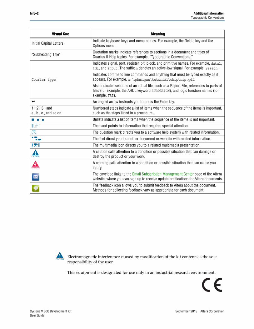
Typographic ConventionsThe following table shows the typographic conventions this document uses.
Date Version Changes
September 2015 1.2 Updates for Rev. E PCB using Enpirion EN23x2 power products.
November 2013 1.1 Updates for production silicon and rev. D PCB using Enperion power products.
May 2013 1.0 Initial release.
Contact (1) Contact Method Address
Technical support Website www.altera.com/support
Technical trainingWebsite www.altera.com/training
Email [email protected]
Product literature Website www.altera.com/literature
Nontechnical support (general) Email [email protected]
(software licensing) Email [email protected]
Note to Table:
(1) You can also contact your local Altera sales office or sales representative.
Visual Cue Meaning
Bold Type with Initial Capital Letters
Indicate command names, dialog box titles, dialog box options, and other GUI labels. For example, Save As dialog box. For GUI elements, capitalization matches the GUI.
bold typeIndicates directory names, project names, disk drive names, file names, file name extensions, software utility names, and GUI labels. For example, \qdesigns directory, D: drive, and chiptrip.gdf file.
Italic Type with Initial Capital Letters Indicate document titles. For example, Stratix IV Design Guidelines.
italic typeIndicates variables. For example, n + 1.
Variable names are enclosed in angle brackets (< >). For example, <file name> and <project name>.pof file.
Cyclone V SoC Development KitUser Guide
Info–2 Additional InformationTypographic Conventions
c Electromagnetic interference caused by modification of the kit contents is the sole responsibility of the user.
This equipment is designated for use only in an industrial research environment.
Initial Capital Letters Indicate keyboard keys and menu names. For example, the Delete key and the Options menu.
“Subheading Title” Quotation marks indicate references to sections in a document and titles of Quartus II Help topics. For example, “Typographic Conventions.”
Courier type
Indicates signal, port, register, bit, block, and primitive names. For example, data1, tdi, and input. The suffix n denotes an active-low signal. For example, resetn.
Indicates command line commands and anything that must be typed exactly as it appears. For example, c:\qdesigns\tutorial\chiptrip.gdf.
Also indicates sections of an actual file, such as a Report File, references to parts of files (for example, the AHDL keyword SUBDESIGN), and logic function names (for example, TRI).
r An angled arrow instructs you to press the Enter key.
1., 2., 3., anda., b., c., and so on
Numbered steps indicate a list of items when the sequence of the items is important, such as the steps listed in a procedure.
■ ■ ■ Bullets indicate a list of items when the sequence of the items is not important.
1 The hand points to information that requires special attention.
h The question mark directs you to a software help system with related information.
f The feet direct you to another document or website with related information.
m The multimedia icon directs you to a related multimedia presentation.
c A caution calls attention to a condition or possible situation that can damage or destroy the product or your work.
w A warning calls attention to a condition or possible situation that can cause you injury.
The envelope links to the Email Subscription Management Center page of the Altera website, where you can sign up to receive update notifications for Altera documents.
The feedback icon allows you to submit feedback to Altera about the document. Methods for collecting feedback vary as appropriate for each document.
Visual Cue Meaning
Cyclone V SoC Development Kit September 2015 Altera CorporationUser Guide