Cyclone V GX Starter Kit User Manual 1 June 5 ...
103
Cyclone V GX Starter Kit User Manual 1 www.terasic.com June 5, 2014
Transcript of Cyclone V GX Starter Kit User Manual 1 June 5 ...
Cyclone V GX Starter Kit
User Manual
1
www.terasic.com
June 5, 2014
Cyclone V GX Starter Kit
User Manual
1
www.terasic.com
June 5, 2014
CONTENTS
CHAPTER 1 INTRODUCTION .................................................................................................... 3
1.1 PACKAGE CONTENTS ............................................................................................................................................... 3
1.2 CYCLONE V GX STARTER KIT SYSTEM CD ............................................................................................................ 4
1.3 LAYOUT AND COMPONENTS .................................................................................................................................... 4
1.4 BLOCK DIAGRAM OF THE CYCLONE V GX STARTER BOARD .................................................................................. 7
1.5 GETTING HELP ........................................................................................................................................................ 7
CHAPTER 2 CONTROL PANEL ................................................................................................... 9
2.1 CONTROL PANEL SETUP .......................................................................................................................................... 9
2.2 CONTROLLING THE LEDS, 7-SEGMENT DISPLAYS ................................................................................................. 12
2.3 SWITCHES AND PUSH-BUTTONS ............................................................................................................................ 14
2.4 SRAM/LPDDR2 CONTROLLER AND PROGRAMMER ............................................................................................. 15
2.5 SD CARD .............................................................................................................................................................. 17
2.6 ADC ..................................................................................................................................................................... 18
2.7 UART-USB COMMUNICATION .............................................................................................................................. 18
2.8 HDMI-TX ............................................................................................................................................................ 20
2.9 HSMC .................................................................................................................................................................. 21
2.10 OVERALL STRUCTURE OF THE C5G CONTROL PANEL ......................................................................................... 22
CHAPTER 3 USING THE STARTER KIT ............................................................................... 24
3.1 CONFIGURATION, STATUS AND SETUP ................................................................................................................... 24
3.2 GENERAL USER INPUT/OUTPUT ............................................................................................................................ 29
3.3 CLOCK CIRCUIT .................................................................................................................................................... 34
3.4 RS-232 SERIAL PORT TO USB INTERFACE ............................................................................................................. 36
3.5 SRAM : STATIC RANDOM ACCESS MEMORY ........................................................................................................ 37
3.6 LPDDR2 MEMORY ............................................................................................................................................... 38
3.7 MICRO SD-CARD .................................................................................................................................................. 41
3.8 HDMI TX INTERFACE ........................................................................................................................................... 42
Cyclone V GX Starter Kit
User Manual
2
www.terasic.com
June 5, 2014
3.9 AUDIO INTERFACE ................................................................................................................................................. 44
3.10 HSMC : HIGH-SPEED MEZZANINE CARD ........................................................................................................... 45
3.11 USING THE 2X20 GPIO EXPANSION HEADER ...................................................................................................... 50
CHAPTER 4 SYSTEM BUILDER ................................................................................................ 59
4.1 INTRODUCTION ..................................................................................................................................................... 59
4.2 GENERAL DESIGN FLOW ....................................................................................................................................... 59
4.3 USING C5G SYSTEM BUILDER .............................................................................................................................. 60
CHAPTER 5 RTL BASED EXAMPLE CODES ........................................................................... 66
5.1 FACTORY CONFIGURATION .................................................................................................................................... 66
5.2 LPDDR2 SDRAM RTL TEST ............................................................................................................................... 67
5.3 SRAM RTL TEST .................................................................................................................................................. 69
CHAPTER 6 NIOS-II BASED EXAMPLE CODES ...................................................................... 71
6.1 SRAM .................................................................................................................................................................. 71
6.2 UART TO USB CONTROL LED ............................................................................................................................. 73
6.3 HDMI TX ............................................................................................................................................................. 77
6.4 TRANSCEIVER HSMC LOOPBACK TEST ................................................................................................................ 83
6.5 AUDIO RECORDING AND PLAYING ......................................................................................................................... 85
6.6 MICRO SD CARD FILE SYSTEM READ .................................................................................................................... 87
6.7 SD CARD MUSIC PLAYER DEMONSTRATION ........................................................................................................... 91
6.8 ADC READING ...................................................................................................................................................... 94
6.9 LPDDR2 SDRAM TEST BY NIOS II............................................................................................................................ 99
ADDITIONAL INFORMATION .............................................................................................................. 102

Cyclone V GX Starter Kit
User Manual
3
www.terasic.com
June 5, 2014
Chapter 1
Introduction
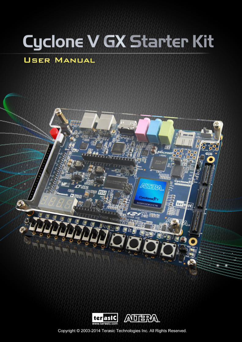
The Cyclone V GX Starter Kit presents a robust hardware design platform built around the Altera
Cyclone V GX FPGA, which is optimized for the lowest cost and power requirement for transceiver
applications with industry-leading programmable logic for ultimate design flexibility. With Cyclone
V FPGAs, you can get the power, cost, and performance levels you need for high-volume
applications including protocol bridging, motor control drives, broadcast video converter and
capture cards, and handheld devices. The Cyclone V GX Starter Kit development board includes
hardware such as Arduino Header, on-board USB Blaster, audio and video capabilities and much
more. In addition, an on-board HSMC connector with high-speed transceivers allows for an even
greater array of hardware setups. By leveraging all of these capabilities, the Cyclone V GX Starter
Kit is the perfect solution for showcasing, evaluating, and prototyping the true potential of the
Altera Cyclone V GX FPGA.
The Cyclone V GX Starter Kit contains all components needed to use the board in conjunction with
a computer that runs the Microsoft Windows XP or later.
11..11 PPaacckkaaggee CCoonntteennttss
Figure 1-1 shows a photograph of the Cyclone V GX Starter Kit package.
Figure 1-1 The Cyclone V GX Starter Kit package contents
The Cyclone V GX Starter Kit package includes:
The Cyclone V GX Starter board
Quick Start Guide
12V DC Power Supply
Type A Male to Type B Male USB Cable
Cyclone V GX Starter Kit
User Manual
4
www.terasic.com
June 5, 2014
11..22 CCyycclloonnee VV GGXX SSttaarrtteerr KKiitt SSyysstteemm CCDD
The Cyclone V GX Start Kit (C5G) System CD contains the documentation and supporting
materials, including the User Manual, Control Panel, System Builder, reference designs and device
datasheets. User can download this System CD from the web (http://www.c5g.terasic.com).
11..33 LLaayyoouutt aanndd CCoommppoonneennttss
This section presents the features and design characteristics of the board.
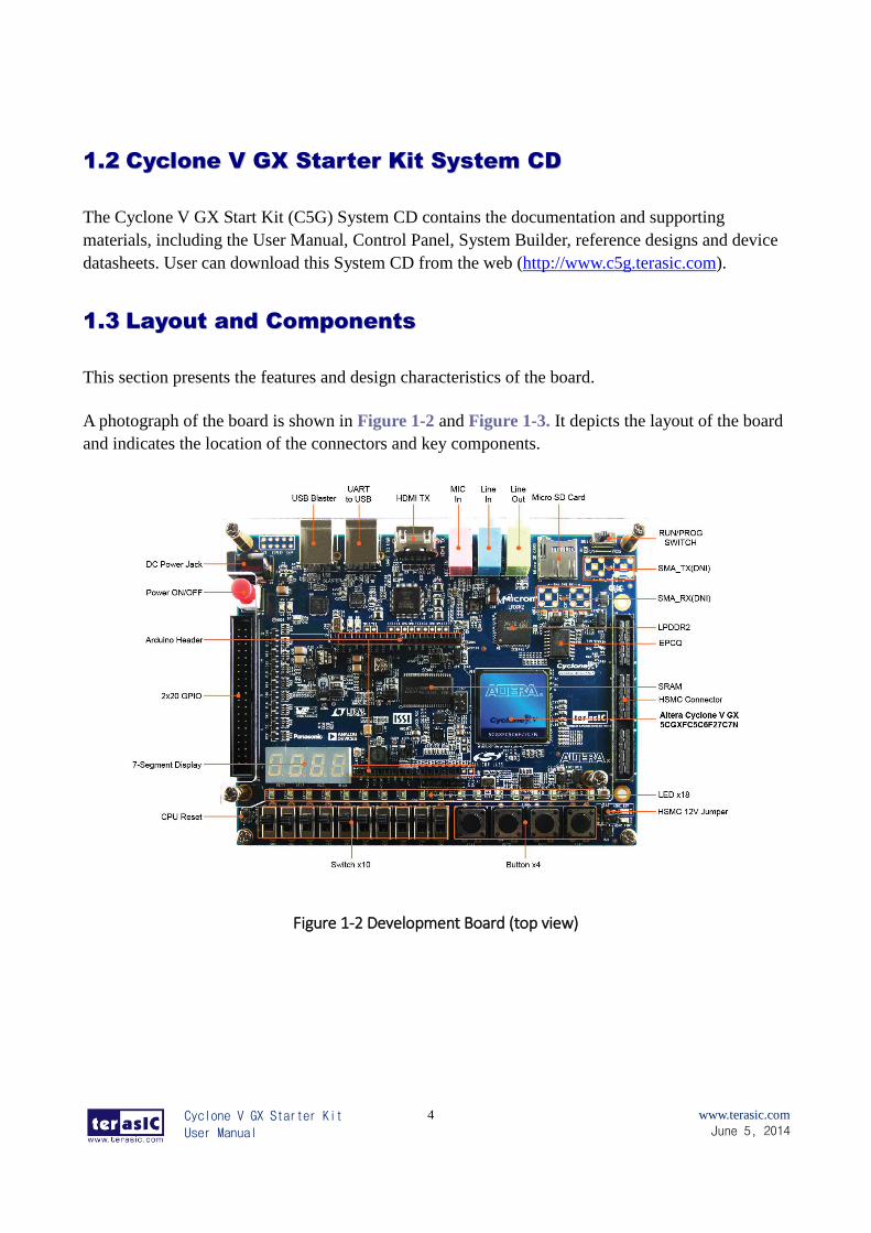
A photograph of the board is shown in Figure 1-2 and Figure 1-3. It depicts the layout of the board
and indicates the location of the connectors and key components.
Figure 1-2 Development Board (top view)
Cyclone V GX Starter Kit
User Manual
5
www.terasic.com
June 5, 2014
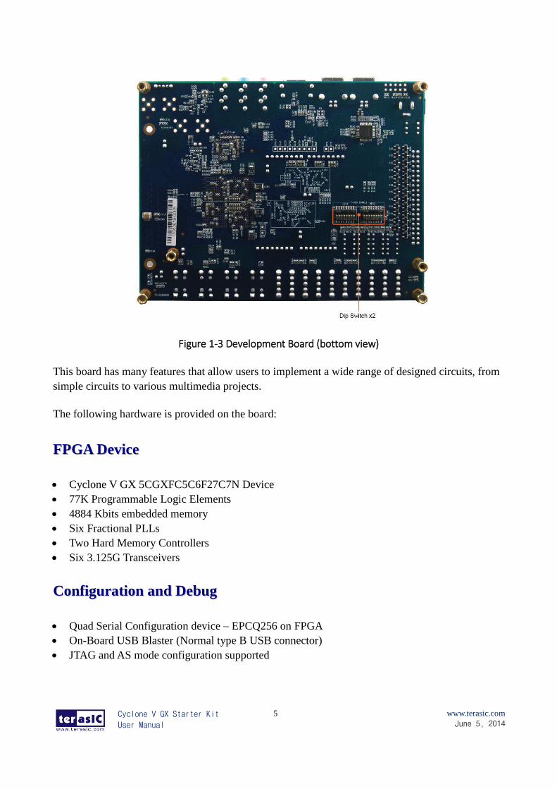
Figure 1-3 Development Board (bottom view)
This board has many features that allow users to implement a wide range of designed circuits, from
simple circuits to various multimedia projects.
The following hardware is provided on the board:
FFPPGGAA DDeevviiccee
Cyclone V GX 5CGXFC5C6F27C7N Device
77K Programmable Logic Elements
4884 Kbits embedded memory
Six Fractional PLLs
Two Hard Memory Controllers
Six 3.125G Transceivers
CCoonnffiigguurraattiioonn aanndd DDeebbuugg
Quad Serial Configuration device – EPCQ256 on FPGA
On-Board USB Blaster (Normal type B USB connector)
JTAG and AS mode configuration supported
Cyclone V GX Starter Kit
User Manual
6
www.terasic.com
June 5, 2014
MMeemmoorryy DDeevviiccee
4Gb LPDDR2 x32 bits data bus
4Mb SRAM x16 bits data bus
CCoommmmuunniiccaattiioonn
UART to USB
CCoonnnneeccttoorrss
HSMC x 1, including 4-lanes 3.125G transceiver,
2x20 GPIO Header
Arduino header, including analog pins.
SMA x 4 (DNI), one-lane 3.125G transceiver
DDiissppllaayy
HDMI TX, compatible with DVI v1.0 and HDCP v1.4
AAuuddiioo
24-bit CODEC, Line-in, line-out, and microphone-in jacks
MMiiccrroo SSDD CCaarrdd SSoocckkeett
Provides SPI and 4-bit SD mode for SD Card access
AADDCC
12-Bit Resolution, 500Ksps Sampling Rate. SPI Interface.
8-Channel Analog Input. Input Range : 0V ~ 4.096V.
SSwwiittcchheess,, BBuuttttoonnss aanndd LLEEDDss
18 LEDs
10 Slide Switches
Cyclone V GX Starter Kit
User Manual
7
www.terasic.com
June 5, 2014
4 Debounced Push Buttons
1 CPU reset Push Buttons
Four 7-Segments
PPoowweerr
12V DC input
11..44 BBlloocckk DDiiaaggrraamm ooff tthhee CCyycclloonnee VV GGXX SSttaarrtteerr BBooaarrdd
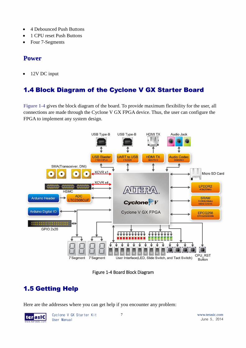
Figure 1-4 gives the block diagram of the board. To provide maximum flexibility for the user, all
connections are made through the Cyclone V GX FPGA device. Thus, the user can configure the
FPGA to implement any system design.
Figure 1-4 Board Block Diagram
11..55 GGeettttiinngg HHeellpp
Here are the addresses where you can get help if you encounter any problem:
Cyclone V GX Starter Kit
User Manual
8
www.terasic.com
June 5, 2014
Terasic Technologies
Taiwan/ 9F, No.176, Sec.2, Gongdao 5th Rd, East Dist, Hsinchu City, Taiwan 300-70
Email: [email protected]
Tel.: +886-3-5750-880
Web: http://www.c5g.terasic.com
Cyclone V GX Starter Kit
User Manual
9
www.terasic.com
June 5, 2014
Chapter 2
Control Panel
The Cyclone V GX Starter board comes with a Control Panel program that allows users to access
various components on the board from a host computer. The host computer communicates with the
board through a USB connection. The program can be used to verify the functionality of
components on the board or be used as a debug tool while developing any RTL code.
This chapter first presents some basic functions of the Control Panel, then describes its structure in
the block diagram form, and finally describes its capabilities.
22..11 CCoonnttrrooll PPaanneell SSeettuupp
The Control Panel Software Utility is located in the directory “Tools/ControlPanel” on the Cyclone
V GX Starter Kit System CD. It's free of installation, just copy the whole folder to your host
computer and launch the control panel by executing the “C5G_ControlPanel.exe”.
Specific control circuits should be downloaded to your FPGA board before the control panel can
request it to perform required tasks. The program will call Quartus II tools to download the control
circuit to the FPGA board through the USB-Blaster[USB-0] connection.
To activate the Control Panel, perform the following steps:
1. Make sure Quartus II 13.1 or a later version is installed successfully on your PC.
2. Set the RUN/PROG switch to the RUN position.
3. Connect the USB cable provided to the USB Blaster port, connect the 12V power supply, and
turn the power switch ON.
4. Start the executable C5G_ControlPanel.exe on the host computer. The Control Panel user
interface shown in Figure 2-1 will appear.
5. The C5G_ControlPanel.sof bit stream is loaded automatically as soon as the
C5G_ControlPanel.exe is launched.
Cyclone V GX Starter Kit
User Manual
10
www.terasic.com
June 5, 2014
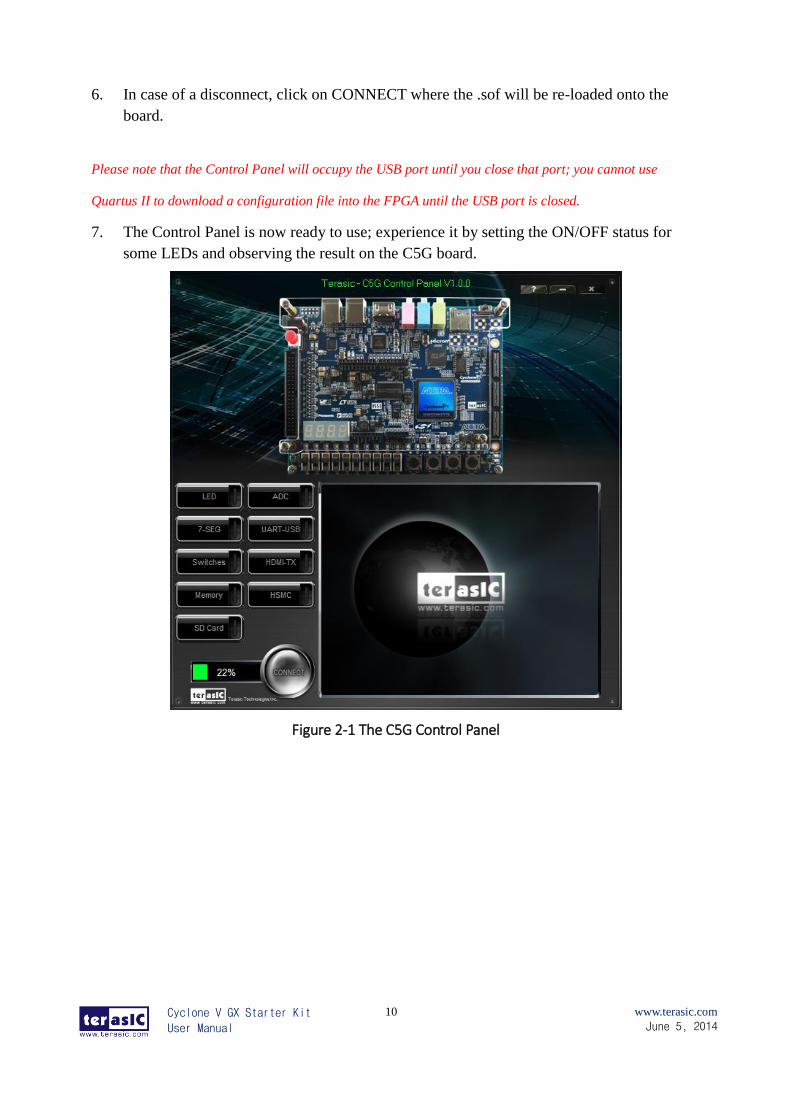
6. In case of a disconnect, click on CONNECT where the .sof will be re-loaded onto the
board.
Please note that the Control Panel will occupy the USB port until you close that port; you cannot use
Quartus II to download a configuration file into the FPGA until the USB port is closed.
7. The Control Panel is now ready to use; experience it by setting the ON/OFF status for
some LEDs and observing the result on the C5G board.
Figure 2-1 The C5G Control Panel
Cyclone V GX Starter Kit
User Manual
11
www.terasic.com
June 5, 2014
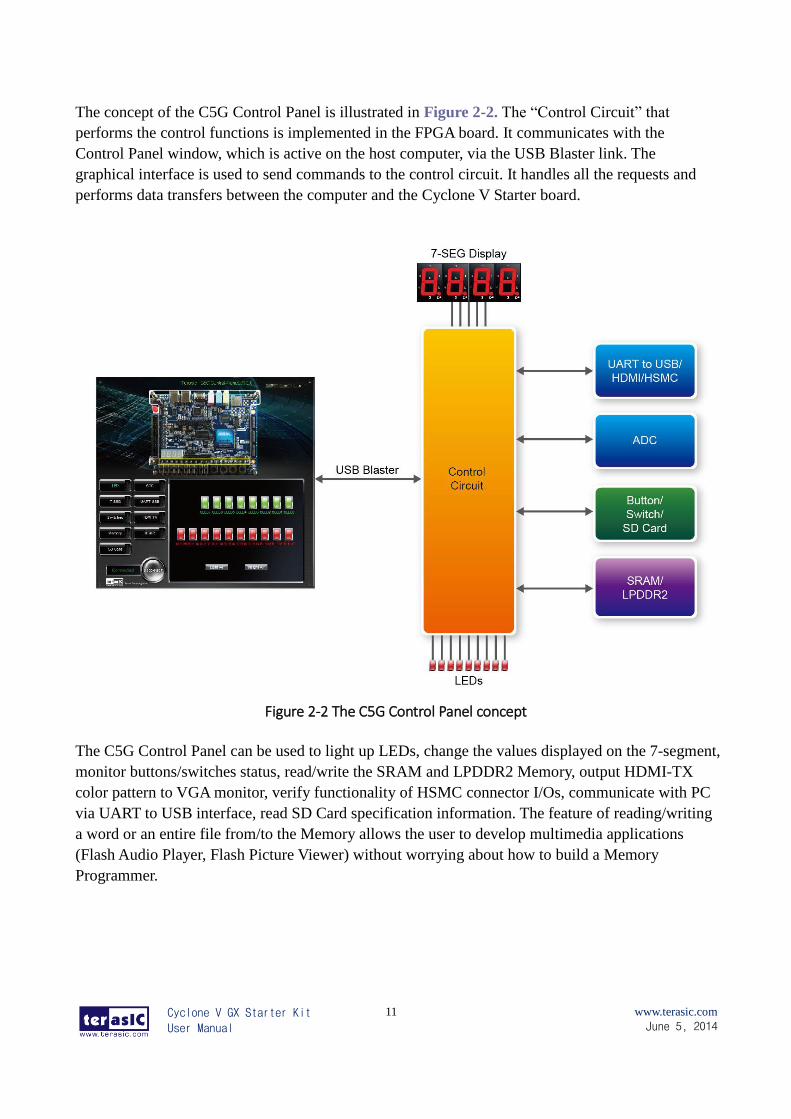
The concept of the C5G Control Panel is illustrated in Figure 2-2. The “Control Circuit” that
performs the control functions is implemented in the FPGA board. It communicates with the
Control Panel window, which is active on the host computer, via the USB Blaster link. The
graphical interface is used to send commands to the control circuit. It handles all the requests and
performs data transfers between the computer and the Cyclone V Starter board.
Figure 2-2 The C5G Control Panel concept
The C5G Control Panel can be used to light up LEDs, change the values displayed on the 7-segment,
monitor buttons/switches status, read/write the SRAM and LPDDR2 Memory, output HDMI-TX
color pattern to VGA monitor, verify functionality of HSMC connector I/Os, communicate with PC
via UART to USB interface, read SD Card specification information. The feature of reading/writing
a word or an entire file from/to the Memory allows the user to develop multimedia applications
(Flash Audio Player, Flash Picture Viewer) without worrying about how to build a Memory
Programmer.
Cyclone V GX Starter Kit
User Manual
12
www.terasic.com
June 5, 2014
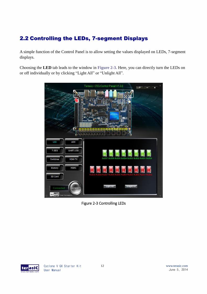
22..22 CCoonnttrroolllliinngg tthhee LLEEDDss,, 77--sseeggmmeenntt DDiissppllaayyss
A simple function of the Control Panel is to allow setting the values displayed on LEDs, 7-segment
displays.
Choosing the LED tab leads to the window in Figure 2-3. Here, you can directly turn the LEDs on
or off individually or by clicking “Light All” or “Unlight All”.
Figure 2-3 Controlling LEDs
Cyclone V GX Starter Kit
User Manual
13
www.terasic.com
June 5, 2014
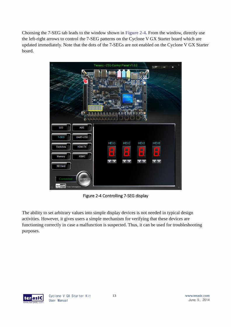
Choosing the 7-SEG tab leads to the window shown in Figure 2-4. From the window, directly use
the left-right arrows to control the 7-SEG patterns on the Cyclone V GX Starter board which are
updated immediately. Note that the dots of the 7-SEGs are not enabled on the Cyclone V GX Starter
board.
Figure 2-4 Controlling 7-SEG display
The ability to set arbitrary values into simple display devices is not needed in typical design
activities. However, it gives users a simple mechanism for verifying that these devices are
functioning correctly in case a malfunction is suspected. Thus, it can be used for troubleshooting
purposes.
Cyclone V GX Starter Kit
User Manual
14
www.terasic.com
June 5, 2014
22..33 SSwwiittcchheess aanndd PPuusshh--bbuuttttoonnss
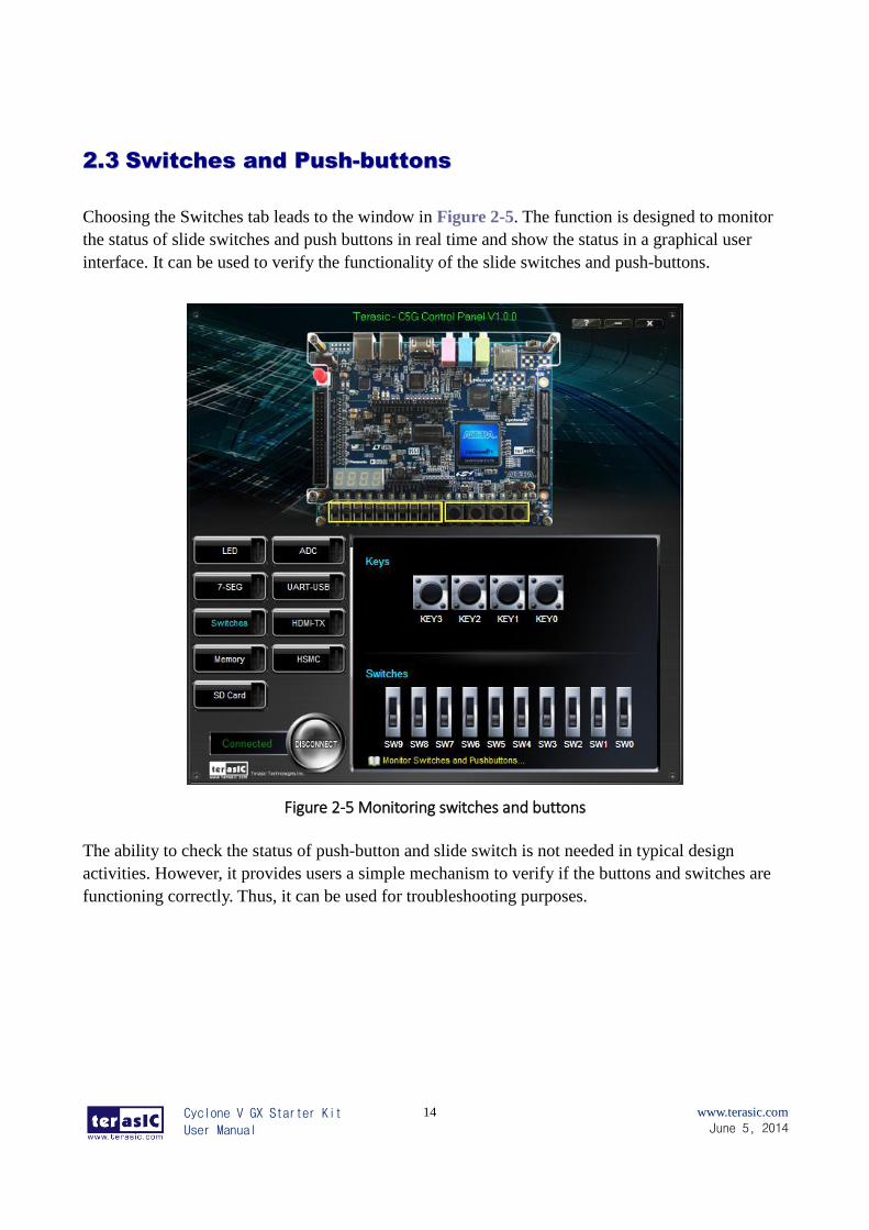
Choosing the Switches tab leads to the window in Figure 2-5. The function is designed to monitor
the status of slide switches and push buttons in real time and show the status in a graphical user
interface. It can be used to verify the functionality of the slide switches and push-buttons.
Figure 2-5 Monitoring switches and buttons
The ability to check the status of push-button and slide switch is not needed in typical design
activities. However, it provides users a simple mechanism to verify if the buttons and switches are
functioning correctly. Thus, it can be used for troubleshooting purposes.
Cyclone V GX Starter Kit
User Manual
15
www.terasic.com
June 5, 2014
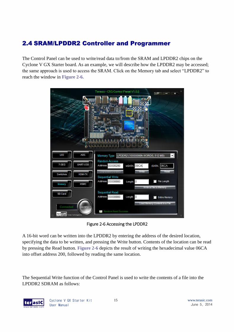
22..44 SSRRAAMM//LLPPDDDDRR22 CCoonnttrroolllleerr aanndd PPrrooggrraammmmeerr
The Control Panel can be used to write/read data to/from the SRAM and LPDDR2 chips on the
Cyclone V GX Starter board. As an example, we will describe how the LPDDR2 may be accessed;
the same approach is used to access the SRAM. Click on the Memory tab and select “LPDDR2” to
reach the window in Figure 2-6.
Figure 2-6 Accessing the LPDDR2
A 16-bit word can be written into the LPDDR2 by entering the address of the desired location,
specifying the data to be written, and pressing the Write button. Contents of the location can be read
by pressing the Read button. Figure 2-6 depicts the result of writing the hexadecimal value 06CA
into offset address 200, followed by reading the same location.
The Sequential Write function of the Control Panel is used to write the contents of a file into the
LPDDR2 SDRAM as follows:
Cyclone V GX Starter Kit
User Manual
16
www.terasic.com
June 5, 2014
1. Specify the starting address in the Address box.
2. Specify the number of bytes to be written in the Length box. If the entire file is to be
loaded, then a check mark may be placed in the File Length box instead of giving the
number of bytes.
3. To initiate the writing process, click on the Write a File to Memory button.
4. When the Control Panel responds with the standard Windows dialog box asking for the
source file, specify the desired file location in the usual manner.
The Control Panel also supports loading files with a .hex extension. Files with a .hex extension are
ASCII text files that specify memory values using ASCII characters to represent hexadecimal
values. For example, a file containing the line
0123456789ABCDEF
defines eight 8-bit values: 01, 23, 45, 67, 89, AB, CD, EF. These values will be loaded
consecutively into the memory.
The Sequential Read function is used to read the contents of the LPDDR2 and fill them into a file as
follows:
1. Specify the starting address in the Address box.
2. Specify the number of bytes to be copied into the file in the Length box. If the entire
contents of the LPDDR2 are to be copied (which involves all 512 Mbytes), then place a
checkmark in the Entire Memory box.
3. Press Load Memory Content to a File button.
4. When the Control Panel responds with the standard Windows dialog box asking for the
destination file, specify the desired file in the usual manner.
Users can use the similar way to access the SRAM.
Cyclone V GX Starter Kit
User Manual
17
www.terasic.com
June 5, 2014
22..55 SSDD CCaarrdd
The function is designed to read the identification and specification information of the SD Card.
The 4-bit SD MODE is used to access the SD Card. This function can be used to verify the
functionality of the SD Card Interface. Follow the steps below to perform the SD Card exercise:
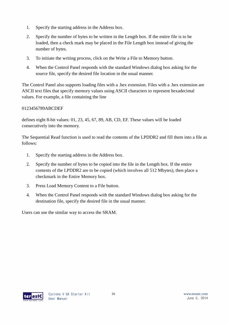
1. Choosing the SD Card tab leads to the window in Figure 2-7.
2. Insert an SD Card to the Cyclone V GX Starter board, and then press the Read button to read
the SD Card. The SD Card’s identification, specification, and file format information will be
displayed in the control window.
Figure 2-7 Reading the SD Card Identification and Specification
Cyclone V GX Starter Kit
User Manual
18
www.terasic.com
June 5, 2014
22..66 AADDCC
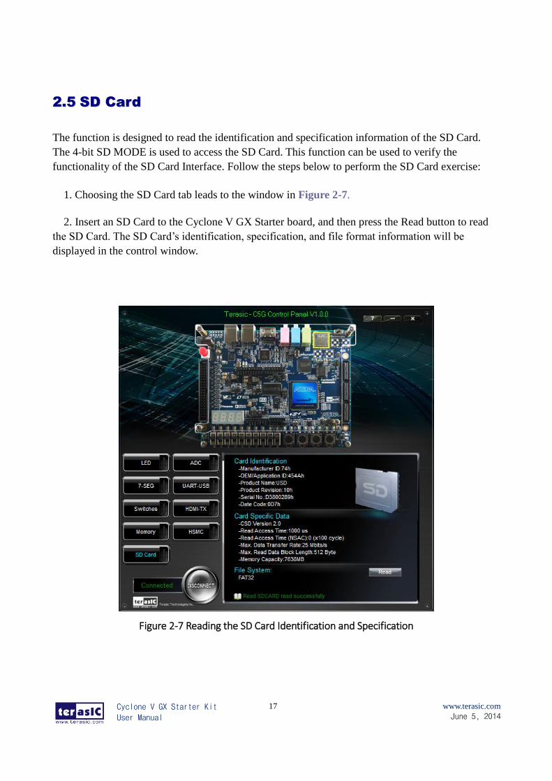
From the Control Panel, users are able to view the eight-channel 12-bit analog-to-digital converter
reading. The values shown are the ADC register outputs from all of the eight separate channels. The
voltage shown is the voltage reading from the separate pins on the extension header. Figure 2-8
shows the ADC readings when the ADC tab is chosen.
Figure 2-8 Reading of eight channel ADC
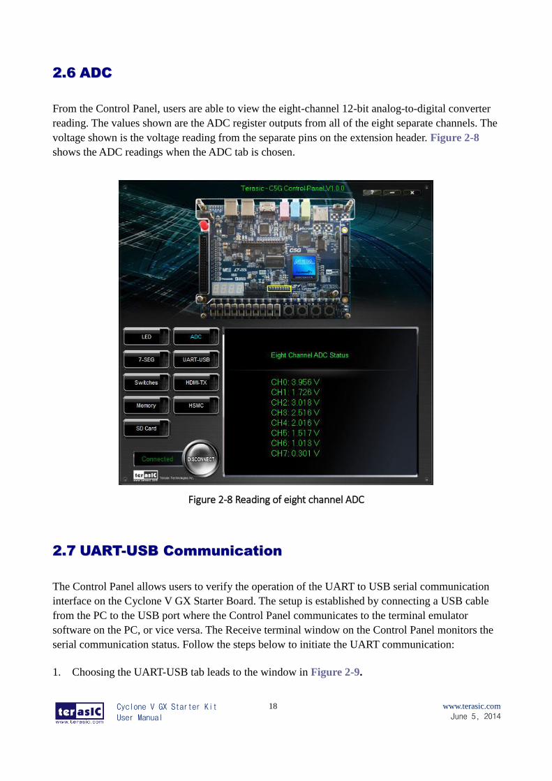
22..77 UUAARRTT--UUSSBB CCoommmmuunniiccaattiioonn
The Control Panel allows users to verify the operation of the UART to USB serial communication
interface on the Cyclone V GX Starter Board. The setup is established by connecting a USB cable
from the PC to the USB port where the Control Panel communicates to the terminal emulator
software on the PC, or vice versa. The Receive terminal window on the Control Panel monitors the
serial communication status. Follow the steps below to initiate the UART communication:
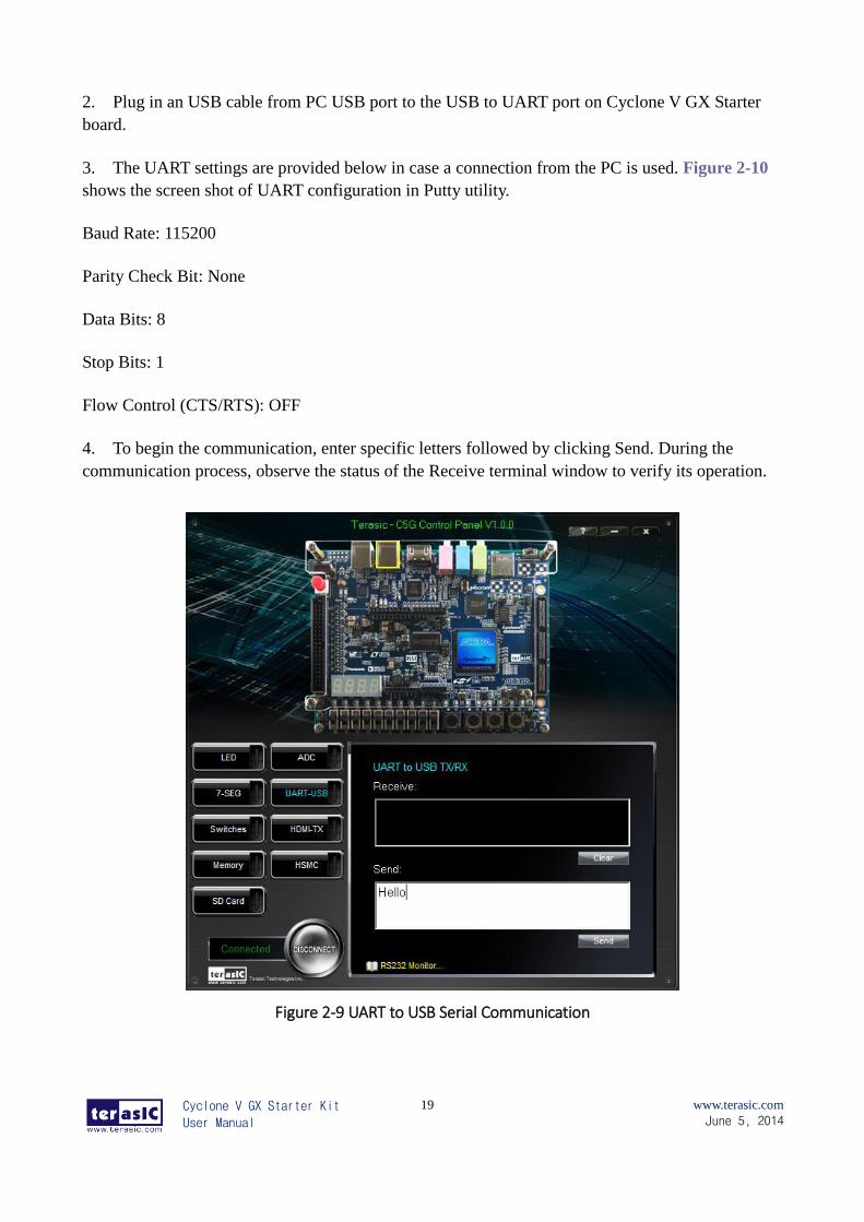
1. Choosing the UART-USB tab leads to the window in Figure 2-9.
Cyclone V GX Starter Kit
User Manual
19
www.terasic.com
June 5, 2014
2. Plug in an USB cable from PC USB port to the USB to UART port on Cyclone V GX Starter
board.
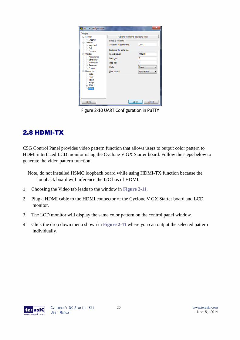
3. The UART settings are provided below in case a connection from the PC is used. Figure 2-10
shows the screen shot of UART configuration in Putty utility.
Baud Rate: 115200
Parity Check Bit: None
Data Bits: 8
Stop Bits: 1
Flow Control (CTS/RTS): OFF
4. To begin the communication, enter specific letters followed by clicking Send. During the
communication process, observe the status of the Receive terminal window to verify its operation.
Figure 2-9 UART to USB Serial Communication
Cyclone V GX Starter Kit
User Manual
20
www.terasic.com
June 5, 2014
Figure 2-10 UART Configuration in PuTTY
22..88 HHDDMMII--TTXX
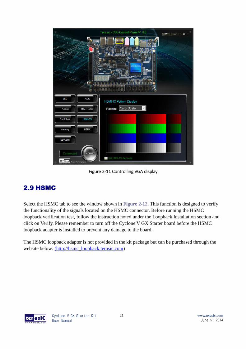
C5G Control Panel provides video pattern function that allows users to output color pattern to
HDMI interfaced LCD monitor using the Cyclone V GX Starter board. Follow the steps below to
generate the video pattern function:
Note, do not installed HSMC loopback board while using HDMI-TX function because the
loopback board will inference the I2C bus of HDMI.
1. Choosing the Video tab leads to the window in Figure 2-11.
2. Plug a HDMI cable to the HDMI connector of the Cyclone V GX Starter board and LCD
monitor.
3. The LCD monitor will display the same color pattern on the control panel window.
4. Click the drop down menu shown in Figure 2-11 where you can output the selected pattern
individually.
Cyclone V GX Starter Kit
User Manual
21
www.terasic.com
June 5, 2014
Figure 2-11 Controlling VGA display
22..99 HHSSMMCC
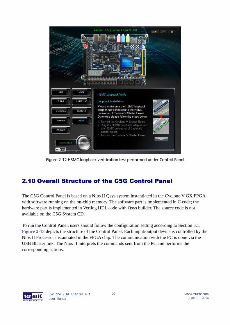
Select the HSMC tab to see the window shown in Figure 2-12. This function is designed to verify
the functionality of the signals located on the HSMC connector. Before running the HSMC
loopback verification test, follow the instruction noted under the Loopback Installation section and
click on Verify. Please remember to turn off the Cyclone V GX Starter board before the HSMC
loopback adapter is installed to prevent any damage to the board.
The HSMC loopback adapter is not provided in the kit package but can be purchased through the
website below: (http://hsmc_loopback.terasic.com)
Cyclone V GX Starter Kit
User Manual
22
www.terasic.com
June 5, 2014
Figure 2-12 HSMC loopback verification test performed under Control Panel
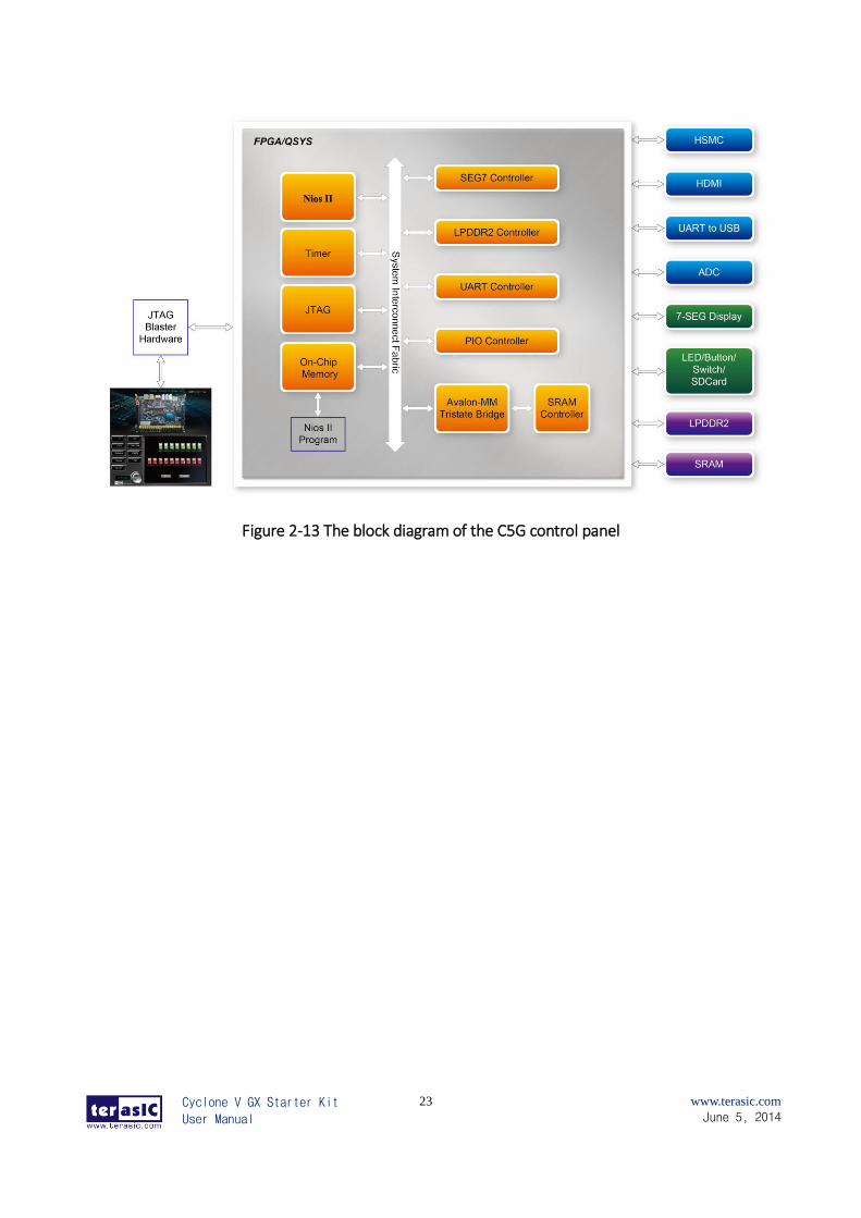
22..1100 OOvveerraallll SSttrruuccttuurree ooff tthhee CC55GG CCoonnttrrooll PPaanneell
The C5G Control Panel is based on a Nios II Qsys system instantiated in the Cyclone V GX FPGA
with software running on the on-chip memory. The software part is implemented in C code; the
hardware part is implemented in Verilog HDL code with Qsys builder. The source code is not
available on the C5G System CD.
To run the Control Panel, users should follow the configuration setting according to Section 3.1.
Figure 2-13 depicts the structure of the Control Panel. Each input/output device is controlled by the
Nios II Processor instantiated in the FPGA chip. The communication with the PC is done via the
USB Blaster link. The Nios II interprets the commands sent from the PC and performs the
corresponding actions.
Cyclone V GX Starter Kit
User Manual
23
www.terasic.com
June 5, 2014
Figure 2-13 The block diagram of the C5G control panel
Cyclone V GX Starter Kit
User Manual
24
www.terasic.com
June 5, 2014
Chapter 3
Using the Starter Kit
In this chapter we introduce the important components on the Cyclone V GX Starter Kit.
33..11 CCoonnffiigguurraattiioonn,, SSttaattuuss aanndd SSeettuupp
The Cyclone V GX Starter board contains a serial configuration device that stores configuration
data for the Cyclone V GX FPGA. This configuration data is automatically loaded from the
configuration device into the FPGA when powered on. Using the Quartus II software, it is possible
to reconfigure the FPGA at any time, and it is also possible to change the non-volatile data that is
stored in the serial configuration device. Both types of programming methods are described below.
1. JTAG programming: In this method of programming, named after the IEEE standards Joint Test
Action Group, the configuration bit stream is downloaded directly into the Cyclone GX FPGA. The
FPGA will retain this configuration as long as power is applied to the board; the configuration
information will be lost when the power is turned off.
2. AS programming: In this method, called Active Serial programming, the configuration bit
stream is downloaded into the Altera EPCQ256 serial configuration device. It provides non-volatile
storage of the bit stream, so that the information is retained even when the power supply to the
Cyclone V GX Starter board is turned off. When the board’s power is turned on, the configuration
data in the EPCQ256 device is automatically loaded into the Cyclone V GX FPGA.
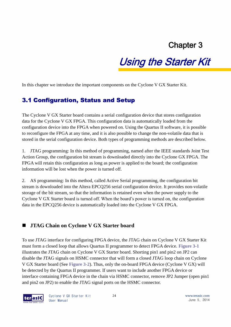
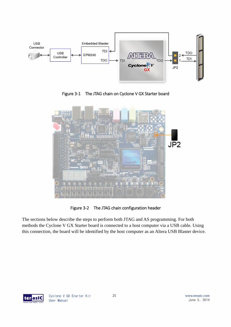
JTAG Chain on Cyclone V GX Starter board
To use JTAG interface for configuring FPGA device, the JTAG chain on Cyclone V GX Starter Kit
must form a closed loop that allows Quartus II programmer to detect FPGA device. Figure 3-1
illustrates the JTAG chain on Cyclone V GX Starter board. Shorting pin1 and pin2 on JP2 can
disable the JTAG signals on HSMC connector that will form a closed JTAG loop chain on Cyclone
V GX Starter board (See Figure 3-2). Thus, only the on-board FPGA device (Cyclone V GX) will
be detected by the Quartus II programmer. If users want to include another FPGA device or
interface containing FPGA device in the chain via HSMC connector, remove JP2 Jumper (open pin1
and pin2 on JP2) to enable the JTAG signal ports on the HSMC connector.
Cyclone V GX Starter Kit
User Manual
25
www.terasic.com
June 5, 2014
Figure 3-1 The JTAG chain on Cyclone V GX Starter board
Figure 3-2 The JTAG chain configuration header
The sections below describe the steps to perform both JTAG and AS programming. For both
methods the Cyclone V GX Starter board is connected to a host computer via a USB cable. Using
this connection, the board will be identified by the host computer as an Altera USB Blaster device.
Cyclone V GX Starter Kit
User Manual
26
www.terasic.com
June 5, 2014
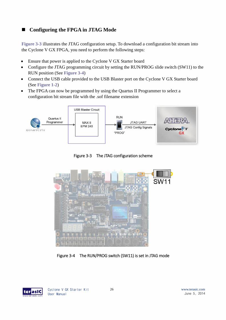
Configuring the FPGA in JTAG Mode
Figure 3-3 illustrates the JTAG configuration setup. To download a configuration bit stream into
the Cyclone V GX FPGA, you need to perform the following steps:
Ensure that power is applied to the Cyclone V GX Starter board
Configure the JTAG programming circuit by setting the RUN/PROG slide switch (SW11) to the
RUN position (See Figure 3-4)
Connect the USB cable provided to the USB Blaster port on the Cyclone V GX Starter board
(See Figure 1-2)
The FPGA can now be programmed by using the Quartus II Programmer to select a
configuration bit stream file with the .sof filename extension
Figure 3-3 The JTAG configuration scheme
Figure 3-4 The RUN/PROG switch (SW11) is set in JTAG mode
Cyclone V GX Starter Kit
User Manual
27
www.terasic.com
June 5, 2014
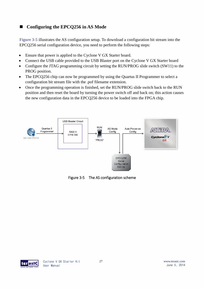
Configuring the EPCQ256 in AS Mode
Figure 3-5 illustrates the AS configuration setup. To download a configuration bit stream into the
EPCQ256 serial configuration device, you need to perform the following steps:
Ensure that power is applied to the Cyclone V GX Starter board.
Connect the USB cable provided to the USB Blaster port on the Cyclone V GX Starter board
Configure the JTAG programming circuit by setting the RUN/PROG slide switch (SW11) to the
PROG position.
The EPCQ256 chip can now be programmed by using the Quartus II Programmer to select a
configuration bit stream file with the .pof filename extension.
Once the programming operation is finished, set the RUN/PROG slide switch back to the RUN
position and then reset the board by turning the power switch off and back on; this action causes
the new configuration data in the EPCQ256 device to be loaded into the FPGA chip.
Figure 3-5 The AS configuration scheme
Cyclone V GX Starter Kit
User Manual
28
www.terasic.com
June 5, 2014
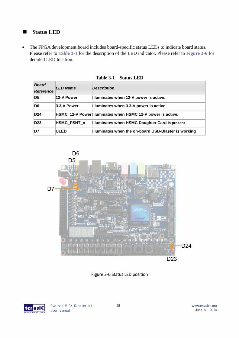
Status LED
The FPGA development board includes board-specific status LEDs to indicate board status.
Please refer to Table 3-1 for the description of the LED indicator. Please refer to Figure 3-6 for
detailed LED location.
Table 3-1 Status LED
Board
Reference LED Name Description
D5 12-V Power Illuminates when 12-V power is active.
D6 3.3-V Power Illuminates when 3.3-V power is active.
D24 HSMC_12-V Power Illuminates when HSMC 12-V power is active.
D23 HSMC_PSNT_n Illuminates when HSMC Daughter Card is present
D7 ULED Illuminates when the on-board USB-Blaster is working
Figure 3-6 Status LED position
Cyclone V GX Starter Kit
User Manual
29
www.terasic.com
June 5, 2014
33..22 GGeenneerraall UUsseerr IInnppuutt//OOuuttppuutt
This section describes the user I/O interface to the FPGA.
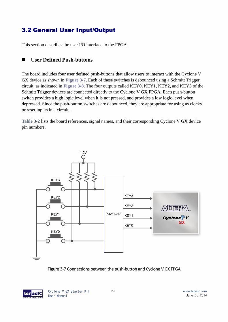
User Defined Push-buttons
The board includes four user defined push-buttons that allow users to interact with the Cyclone V
GX device as shown in Figure 3-7. Each of these switches is debounced using a Schmitt Trigger
circuit, as indicated in Figure 3-8. The four outputs called KEY0, KEY1, KEY2, and KEY3 of the
Schmitt Trigger devices are connected directly to the Cyclone V GX FPGA. Each push-button
switch provides a high logic level when it is not pressed, and provides a low logic level when
depressed. Since the push-button switches are debounced, they are appropriate for using as clocks
or reset inputs in a circuit.
Table 3-2 lists the board references, signal names, and their corresponding Cyclone V GX device
pin numbers.
Figure 3-7 Connections between the push-button and Cyclone V GX FPGA
Cyclone V GX Starter Kit
User Manual
30
www.terasic.com
June 5, 2014
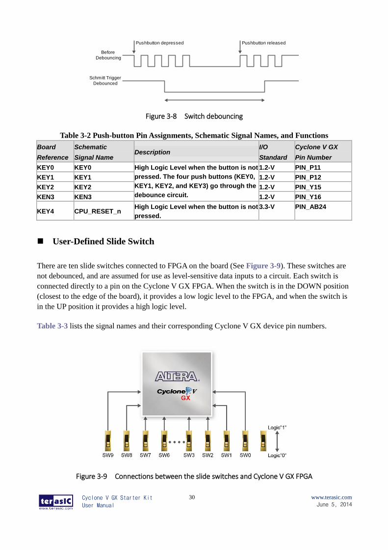
Pushbutton releasedPushbutton depressed
Before
Debouncing
Schmitt Trigger
Debounced
Figure 3-8 Switch debouncing
Table 3-2 Push-button Pin Assignments, Schematic Signal Names, and Functions
Board
Reference
Schematic
Signal Name Description
I/O
Standard
Cyclone V GX
Pin Number
KEY0 KEY0 High Logic Level when the button is not
pressed. The four push buttons (KEY0,
KEY1, KEY2, and KEY3) go through the
debounce circuit.
1.2-V PIN_P11
KEY1 KEY1 1.2-V PIN_P12
KEY2 KEY2 1.2-V PIN_Y15
KEN3 KEN3 1.2-V PIN_Y16
KEY4 CPU_RESET_n High Logic Level when the button is not
pressed.
3.3-V PIN_AB24
User-Defined Slide Switch
There are ten slide switches connected to FPGA on the board (See Figure 3-9). These switches are
not debounced, and are assumed for use as level-sensitive data inputs to a circuit. Each switch is
connected directly to a pin on the Cyclone V GX FPGA. When the switch is in the DOWN position
(closest to the edge of the board), it provides a low logic level to the FPGA, and when the switch is
in the UP position it provides a high logic level.
Table 3-3 lists the signal names and their corresponding Cyclone V GX device pin numbers.
Figure 3-9 Connections between the slide switches and Cyclone V GX FPGA
Cyclone V GX Starter Kit
User Manual
31
www.terasic.com
June 5, 2014
104H104
Table 3-3 Slide Switch Pin Assignments, Schematic Signal Names, and Functions
Board
Reference
Schematic
Signal Name Description
I/O
Standard
Cyclone V GX
Pin Number
SW0 SW0 Slide Switch[0] 1.2-V PIN_AC9
SW1 SW1 Slide Switch[1] 1.2-V PIN_AE10
SW2 SW2 Slide Switch[2] 1.2-V PIN_AD13
SW3 SW3 Slide Switch[3] 1.2-V PIN_AC8
SW4 SW4 Slide Switch[4] 1.2-V PIN_W11
SW5 SW5 Slide Switch[5] 1.2-V PIN_AB10
SW6 SW6 Slide Switch[6] 1.2-V PIN_V10
SW7 SW7 Slide Switch[7] 1.2-V PIN_AC10
SW8 SW8 Slide Switch[8] 1.2-V PIN_Y11
SW9 SW9 Slide Switch[9] 1.2-V PIN_AE19
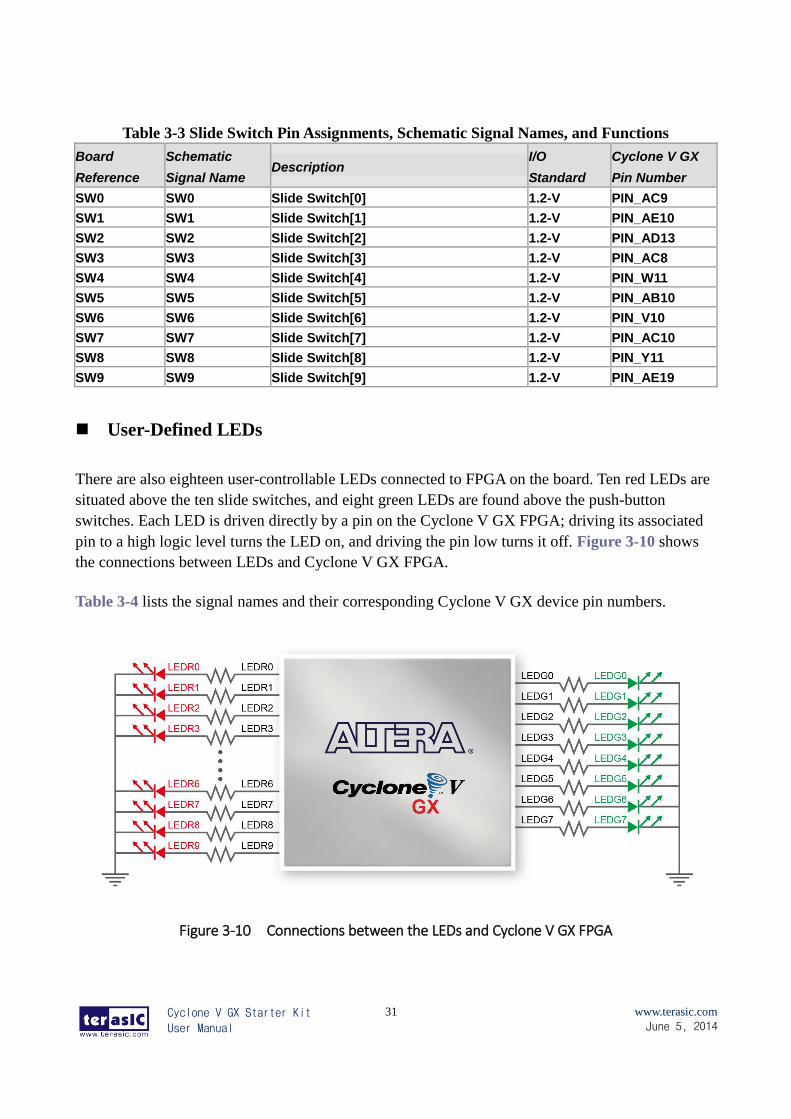
User-Defined LEDs
There are also eighteen user-controllable LEDs connected to FPGA on the board. Ten red LEDs are
situated above the ten slide switches, and eight green LEDs are found above the push-button
switches. Each LED is driven directly by a pin on the Cyclone V GX FPGA; driving its associated
pin to a high logic level turns the LED on, and driving the pin low turns it off. Figure 3-10 shows
the connections between LEDs and Cyclone V GX FPGA.
Table 3-4 lists the signal names and their corresponding Cyclone V GX device pin numbers.
Figure 3-10 Connections between the LEDs and Cyclone V GX FPGA
Cyclone V GX Starter Kit
User Manual
32
www.terasic.com
June 5, 2014
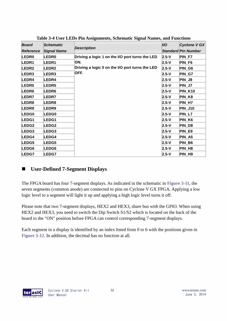
Table 3-4 User LEDs Pin Assignments, Schematic Signal Names, and Functions
Board
Reference
Schematic
Signal Name Description
I/O
Standard
Cyclone V GX
Pin Number
LEDR0 LEDR0 Driving a logic 1 on the I/O port turns the LED
ON.
Driving a logic 0 on the I/O port turns the LED
OFF.
2.5-V PIN_F7
LEDR1 LEDR1 2.5-V PIN_F6
LEDR2 LEDR2 2.5-V PIN_G6
LEDR3 LEDR3 2.5-V PIN_G7
LEDR4 LEDR4 2.5-V PIN_J8
LEDR5 LEDR5 2.5-V PIN_J7
LEDR6 LEDR6 2.5-V PIN_K10
LEDR7 LEDR7 2.5-V PIN_K8
LEDR8 LEDR8 2.5-V PIN_H7
LEDR9 LEDR9 2.5-V PIN_J10
LEDG0 LEDG0 2.5-V PIN_L7
LEDG1 LEDG1 2.5-V PIN_K6
LEDG2 LEDG2 2.5-V PIN_D8
LEDG3 LEDG3 2.5-V PIN_E9
LEDG4 LEDG4 2.5-V PIN_A5
LEDG5 LEDG5 2.5-V PIN_B6
LEDG6 LEDG6 2.5-V PIN_H8
LEDG7 LEDG7 2.5-V PIN_H9
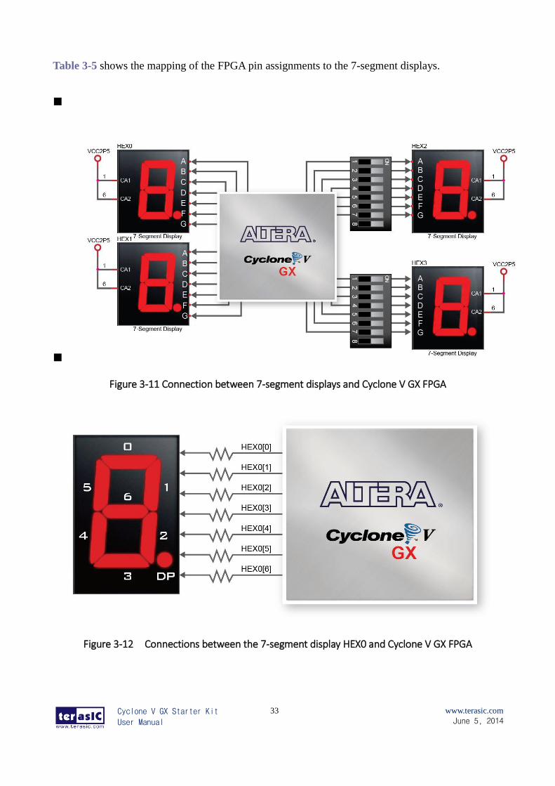
User-Defined 7-Segment Displays
The FPGA board has four 7-segment displays. As indicated in the schematic in Figure 3-11, the
seven segments (common anode) are connected to pins on Cyclone V GX FPGA. Applying a low
logic level to a segment will light it up and applying a high logic level turns it off.
Please note that two 7-segment displays, HEX2 and HEX3, share bus with the GPIO. When using
HEX2 and HEX3, you need to switch the Dip Switch S1/S2 which is located on the back of the
board to the "ON" position before FPGA can control corresponding 7-segment displays.
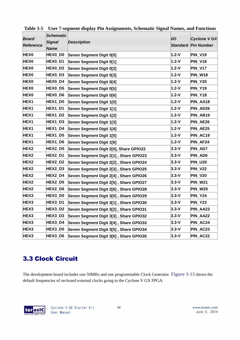
Each segment in a display is identified by an index listed from 0 to 6 with the positions given in
Figure 3-12. In addition, the decimal has no function at all.
Cyclone V GX Starter Kit
User Manual
33
www.terasic.com
June 5, 2014
Table 3-5 shows the mapping of the FPGA pin assignments to the 7-segment displays.
Figure 3-11 Connection between 7-segment displays and Cyclone V GX FPGA
Figure 3-12 Connections between the 7-segment display HEX0 and Cyclone V GX FPGA
Cyclone V GX Starter Kit
User Manual
34
www.terasic.com
June 5, 2014
Table 3-5 User 7-segment display Pin Assignments, Schematic Signal Names, and Functions
Board
Reference
Schematic
Signal
Name
Description I/O
Standard
Cyclone V GX
Pin Number
HEX0 HEX0_D0 Seven Segment Digit 0[0] 1.2-V PIN_V19
HEX0 HEX0_D1 Seven Segment Digit 0[1] 1.2-V PIN_V18
HEX0 HEX0_D2 Seven Segment Digit 0[2] 1.2-V PIN_V17
HEX0 HEX0_D3 Seven Segment Digit 0[3] 1.2-V PIN_W18
HEX0 HEX0_D4 Seven Segment Digit 0[4] 1.2-V PIN_Y20
HEX0 HEX0_D5 Seven Segment Digit 0[5] 1.2-V PIN_Y19
HEX0 HEX0_D6 Seven Segment Digit 0[6] 1.2-V PIN_Y18
HEX1 HEX1_D0 Seven Segment Digit 1[0] 1.2-V PIN_AA18
HEX1 HEX1_D1 Seven Segment Digit 1[1] 1.2-V PIN_AD26
HEX1 HEX1_D2 Seven Segment Digit 1[2] 1.2-V PIN_AB19
HEX1 HEX1_D3 Seven Segment Digit 1[3] 1.2-V PIN_AE26
HEX1 HEX1_D4 Seven Segment Digit 1[4] 1.2-V PIN_AE25
HEX1 HEX1_D5 Seven Segment Digit 1[5] 1.2-V PIN_AC19
HEX1 HEX1_D6 Seven Segment Digit 1[6] 1.2-V PIN_AF24
HEX2 HEX2_D0 Seven Segment Digit 2[0], Share GPIO22 3.3-V PIN_AD7
HEX2 HEX2_D1 Seven Segment Digit 2[1] , Share GPIO23 3.3-V PIN_AD6
HEX2 HEX2_D2 Seven Segment Digit 2[2] , Share GPIO24 3.3-V PIN_U20
HEX2 HEX2_D3 Seven Segment Digit 2[3] , Share GPIO25 3.3-V PIN_V22
HEX2 HEX2_D4 Seven Segment Digit 2[4] , Share GPIO26 3.3-V PIN_V20
HEX2 HEX2_D5 Seven Segment Digit 2[5] , Share GPIO27 3.3-V PIN_W21
HEX2 HEX2_D6 Seven Segment Digit 2[6] , Share GPIO28 3.3-V PIN_W20
HEX3 HEX3_D0 Seven Segment Digit 3[0] , Share GPIO29 3.3-V PIN_Y24
HEX3 HEX3_D1 Seven Segment Digit 3[1] , Share GPIO30 3.3-V PIN_Y23
HEX3 HEX3_D2 Seven Segment Digit 3[2] , Share GPIO31 3.3-V PIN_AA23
HEX3 HEX3_D3 Seven Segment Digit 3[3] , Share GPIO32 3.3-V PIN_AA22
HEX3 HEX3_D4 Seven Segment Digit 3[4] , Share GPIO33 3.3-V PIN_AC24
HEX3 HEX3_D5 Seven Segment Digit 3[5] , Share GPIO34 3.3-V PIN_AC23
HEX3 HEX3_D6 Seven Segment Digit 3[6] , Share GPIO35 3.3-V PIN_AC22
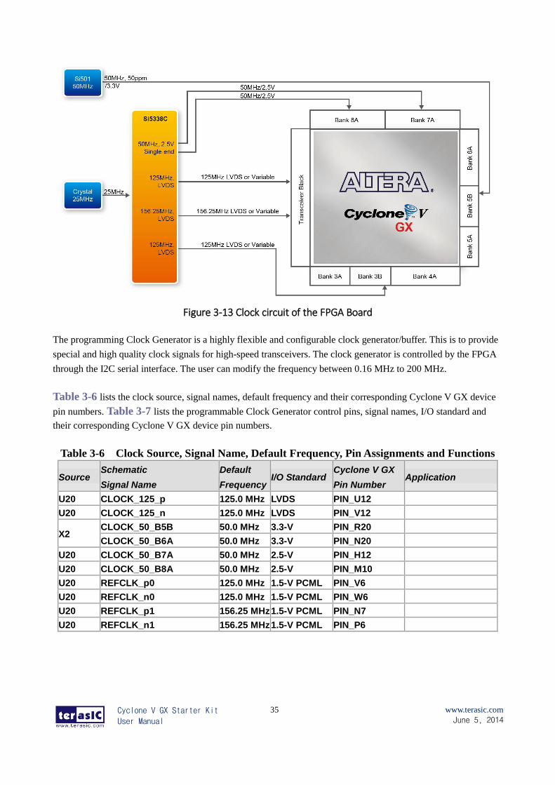
33..33 CClloocckk CCiirrccuuiitt
The development board includes one 50MHz and one programmable Clock Generator. Figure 3-13 shows the
default frequencies of on-board external clocks going to the Cyclone V GX FPGA.
Cyclone V GX Starter Kit
User Manual
35
www.terasic.com
June 5, 2014
Figure 3-13 Clock circuit of the FPGA Board
The programming Clock Generator is a highly flexible and configurable clock generator/buffer. This is to provide
special and high quality clock signals for high-speed transceivers. The clock generator is controlled by the FPGA
through the I2C serial interface. The user can modify the frequency between 0.16 MHz to 200 MHz.
112H112HTable 3-6 lists the clock source, signal names, default frequency and their corresponding Cyclone V GX device
pin numbers. Table 3-7 lists the programmable Clock Generator control pins, signal names, I/O standard and
their corresponding Cyclone V GX device pin numbers.
Table 3-6 Clock Source, Signal Name, Default Frequency, Pin Assignments and Functions
Source Schematic
Signal Name
Default
Frequency I/O Standard
Cyclone V GX
Pin Number Application
U20 CLOCK_125_p 125.0 MHz LVDS PIN_U12
U20 CLOCK_125_n 125.0 MHz LVDS PIN_V12
X2 CLOCK_50_B5B 50.0 MHz 3.3-V PIN_R20
CLOCK_50_B6A 50.0 MHz 3.3-V PIN_N20
U20 CLOCK_50_B7A 50.0 MHz 2.5-V PIN_H12
U20 CLOCK_50_B8A 50.0 MHz 2.5-V PIN_M10
U20 REFCLK_p0 125.0 MHz 1.5-V PCML PIN_V6
U20 REFCLK_n0 125.0 MHz 1.5-V PCML PIN_W6
U20 REFCLK_p1 156.25 MHz 1.5-V PCML PIN_N7
U20 REFCLK_n1 156.25 MHz 1.5-V PCML PIN_P6
113H113H
Cyclone V GX Starter Kit
User Manual
36
www.terasic.com
June 5, 2014
Table 3-7 Programmable oscillator control pin, Signal Name, I/O standard, Pin Assignments
and Descriptions
Programmable
Oscillator
Schematic
Signal Name I/O Standard
Cyclone V GX
Pin Number Description
U20 (Si5338) I2C_SCL 2.5-V PIN_B7 I2C bus, direct
connected with Si5338 I2C_SDA 2.5-V PIN_G11
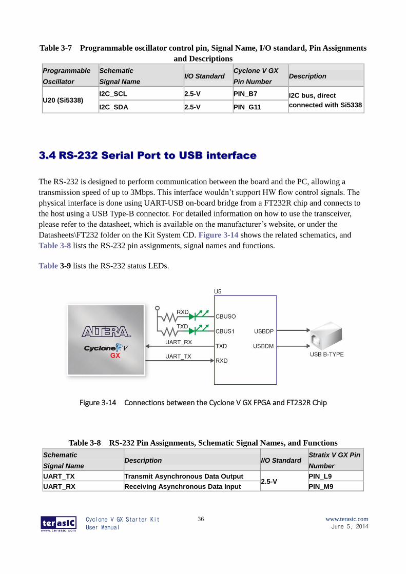
33..44 RRSS--223322 SSeerriiaall PPoorrtt ttoo UUSSBB iinntteerrffaaccee
The RS-232 is designed to perform communication between the board and the PC, allowing a
transmission speed of up to 3Mbps. This interface wouldn’t support HW flow control signals. The
physical interface is done using UART-USB on-board bridge from a FT232R chip and connects to
the host using a USB Type-B connector. For detailed information on how to use the transceiver,
please refer to the datasheet, which is available on the manufacturer’s website, or under the
Datasheets\FT232 folder on the Kit System CD. Figure 3-14 shows the related schematics, and
Table 3-8 lists the RS-232 pin assignments, signal names and functions.
Table 3-9 lists the RS-232 status LEDs.
Figure 3-14 Connections between the Cyclone V GX FPGA and FT232R Chip
15H115H
Table 3-8 RS-232 Pin Assignments, Schematic Signal Names, and Functions
Schematic
Signal Name Description I/O Standard
Stratix V GX Pin
Number
UART_TX Transmit Asynchronous Data Output 2.5-V
PIN_L9
UART_RX Receiving Asynchronous Data Input PIN_M9
Cyclone V GX Starter Kit
User Manual
37
www.terasic.com
June 5, 2014
Table 3-9 RS-232 Status LED
Board Reference LED Name Description
D8 TX LED Illuminates when RS-232 transmission is active.
D9 RX LED Illuminates when RS-232 receiving is active.
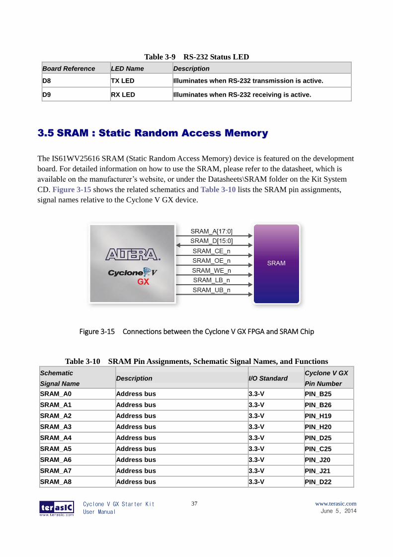
33..55 SSRRAAMM :: SSttaattiicc RRaannddoomm AAcccceessss MMeemmoorryy
The IS61WV25616 SRAM (Static Random Access Memory) device is featured on the development
board. For detailed information on how to use the SRAM, please refer to the datasheet, which is
available on the manufacturer’s website, or under the Datasheets\SRAM folder on the Kit System
CD. Figure 3-15 shows the related schematics and Table 3-10 lists the SRAM pin assignments,
signal names relative to the Cyclone V GX device.
Figure 3-15 Connections between the Cyclone V GX FPGA and SRAM Chip
Table 3-10 SRAM Pin Assignments, Schematic Signal Names, and Functions
Schematic
Signal Name Description I/O Standard
Cyclone V GX
Pin Number
SRAM_A0 Address bus 3.3-V PIN_B25
SRAM_A1 Address bus 3.3-V PIN_B26
SRAM_A2 Address bus 3.3-V PIN_H19
SRAM_A3 Address bus 3.3-V PIN_H20
SRAM_A4 Address bus 3.3-V PIN_D25
SRAM_A5 Address bus 3.3-V PIN_C25
SRAM_A6 Address bus 3.3-V PIN_J20
SRAM_A7 Address bus 3.3-V PIN_J21
SRAM_A8 Address bus 3.3-V PIN_D22
Cyclone V GX Starter Kit
User Manual
38
www.terasic.com
June 5, 2014
SRAM_A9 Address bus 3.3-V PIN_E23
SRAM_A10 Address bus 3.3-V PIN_G20
SRAM_A11 Address bus 3.3-V PIN_F21
SRAM_A12 Address bus 3.3-V PIN_E21
SRAM_A13 Address bus 3.3-V PIN_F22
SRAM_A14 Address bus 3.3-V PIN_J25
SRAM_A15 Address bus 3.3-V PIN_J26
SRAM_A16 Address bus 3.3-V PIN_N24
SRAM_A17 Address bus 3.3-V PIN_M24
SRAM_D0 Data bus 3.3-V PIN_E24
SRAM_D1 Data bus 3.3-V PIN_E25
SRAM_D2 Data bus 3.3-V PIN_K24
SRAM_D3 Data bus 3.3-V PIN_K23
SRAM_D4 Data bus 3.3-V PIN_F24
SRAM_D5 Data bus 3.3-V PIN_G24
SRAM_D6 Data bus 3.3-V PIN_L23
SRAM_D7 Data bus 3.3-V PIN_L24
SRAM_D8 Data bus 3.3-V PIN_H23
SRAM_D9 Data bus 3.3-V PIN_H24
SRAM_D10 Data bus 3.3-V PIN_H22
SRAM_D11 Data bus 3.3-V PIN_J23
SRAM_D12 Data bus 3.3-V PIN_F23
SRAM_D13 Data bus 3.3-V PIN_G22
SRAM_D14 Data bus 3.3-V PIN_L22
SRAM_D15 Data bus 3.3-V PIN_K21
SRAM_CE_n Chip Enable, active Low 3.3-V PIN_N23
SRAM_OE_n Output Enable, active Low 3.3-V PIN_M22
SRAM_WE_n Write Enable, active Low 3.3-V PIN_G25
SRAM_LB_n Lower-Byte Control, D0~D7, active Low 3.3-V PIN_H25
SRAM_UB_n Upper-Byte Control, D8~D15, active Low 3.3-V PIN_M25
33..66 LLPPDDDDRR22 MMeemmoorryy
The development board has one 4Gb Mobile Low-Power DDR2 SDRAM (LPDDR2) which is a
high-speed CMOS, dynamic random-access memory containing 4,294,967,296-bits shown in
Figure 3-16.
For detailed information on how to use the LPDDR2, please refer to the datasheet, which is
available on the manufacturer’s website, or under the Datasheets\LPDDR2 folder on the Kit System
Cyclone V GX Starter Kit
User Manual
39
www.terasic.com
June 5, 2014
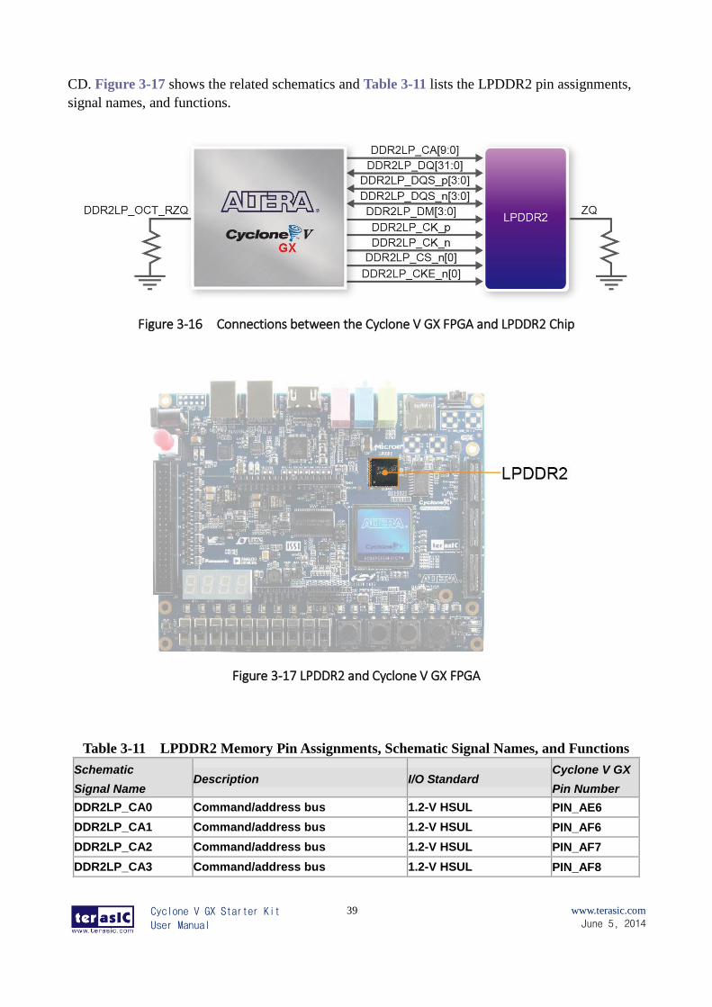
CD. Figure 3-17 shows the related schematics and Table 3-11 lists the LPDDR2 pin assignments,
signal names, and functions.
Figure 3-16 Connections between the Cyclone V GX FPGA and LPDDR2 Chip
Figure 3-17 LPDDR2 and Cyclone V GX FPGA
Table 3-11 LPDDR2 Memory Pin Assignments, Schematic Signal Names, and Functions
Schematic
Signal Name Description I/O Standard
Cyclone V GX
Pin Number
DDR2LP_CA0 Command/address bus 1.2-V HSUL PIN_AE6
DDR2LP_CA1 Command/address bus 1.2-V HSUL PIN_AF6
DDR2LP_CA2 Command/address bus 1.2-V HSUL PIN_AF7
DDR2LP_CA3 Command/address bus 1.2-V HSUL PIN_AF8
Cyclone V GX Starter Kit
User Manual
40
www.terasic.com
June 5, 2014
DDR2LP_CA4 Command/address bus 1.2-V HSUL PIN_U10
DDR2LP_CA5 Command/address bus 1.2-V HSUL PIN_U11
DDR2LP_CA6 Command/address bus 1.2-V HSUL PIN_AE9
DDR2LP_CA7 Command/address bus 1.2-V HSUL PIN_AF9
DDR2LP_CA8 Command/address bus 1.2-V HSUL PIN_AB12
DDR2LP_CA9 Command/address bus 1.2-V HSUL PIN_AB11
DDR2LP_DQ0 Data bus 1.2-V HSUL PIN_AA14
DDR2LP_DQ1 Data bus 1.2-V HSUL PIN_Y14
DDR2LP_DQ2 Data bus 1.2-V HSUL PIN_AD11
DDR2LP_DQ3 Data bus 1.2-V HSUL PIN_AD12
DDR2LP_DQ4 Data bus 1.2-V HSUL PIN_Y13
DDR2LP_DQ5 Data bus 1.2-V HSUL PIN_W12
DDR2LP_DQ6 Data bus 1.2-V HSUL PIN_AD10
DDR2LP_DQ7 Data bus 1.2-V HSUL PIN_AF12
DDR2LP_DQ8 Data bus 1.2-V HSUL PIN_AC15
DDR2LP_DQ9 Data bus 1.2-V HSUL PIN_AB15
DDR2LP_DQ10 Data bus 1.2-V HSUL PIN_AC14
DDR2LP_DQ11 Data bus 1.2-V HSUL PIN_AF13
DDR2LP_DQ12 Data bus 1.2-V HSUL PIN_AB16
DDR2LP_DQ13 Data bus 1.2-V HSUL PIN_AA16
DDR2LP_DQ14 Data bus 1.2-V HSUL PIN_AE14
DDR2LP_DQ15 Data bus 1.2-V HSUL PIN_AF18
DDR2LP_DQ16 Data bus 1.2-V HSUL PIN_AD16
DDR2LP_DQ17 Data bus 1.2-V HSUL PIN_AD17
DDR2LP_DQ18 Data bus 1.2-V HSUL PIN_AC18
DDR2LP_DQ19 Data bus 1.2-V HSUL PIN_AF19
DDR2LP_DQ20 Data bus 1.2-V HSUL PIN_AC17
DDR2LP_DQ21 Data bus 1.2-V HSUL PIN_AB17
DDR2LP_DQ22 Data bus 1.2-V HSUL PIN_AF21
DDR2LP_DQ23 Data bus 1.2-V HSUL PIN_AE21
DDR2LP_DQ24 Data bus 1.2-V HSUL PIN_AE15
DDR2LP_DQ25 Data bus 1.2-V HSUL PIN_AE16
DDR2LP_DQ26 Data bus 1.2-V HSUL PIN_AC20
DDR2LP_DQ27 Data bus 1.2-V HSUL PIN_AD21
DDR2LP_DQ28 Data bus 1.2-V HSUL PIN_AF16
DDR2LP_DQ29 Data bus 1.2-V HSUL PIN_AF17
DDR2LP_DQ30 Data bus 1.2-V HSUL PIN_AD23
DDR2LP_DQ31 Data bus 1.2-V HSUL PIN_AF23
DDR2LP_DQS_p0 Data Strobe positive Differential 1.2-V HSUL PIN_V13
DDR2LP_DQS_p1 Data Strobe positive Differential 1.2-V HSUL PIN_U14
DDR2LP_DQS_p2 Data Strobe positive Differential 1.2-V HSUL PIN_V15
Cyclone V GX Starter Kit
User Manual
41
www.terasic.com
June 5, 2014
DDR2LP_DQS_p3 Data Strobe positive Differential 1.2-V HSUL PIN_W16
DDR2LP_DQS_n0 Data Strobe negative Differential 1.2-V HSUL PIN_W13
DDR2LP_DQS_n1 Data Strobe negative Differential 1.2-V HSUL PIN_V14
DDR2LP_DQS_n2 Data Strobe negative Differential 1.2-V HSUL PIN_W15
DDR2LP_DQS_n3 Data Strobe negative Differential 1.2-V HSUL PIN_W17
DDR2LP_DM0 Data Write Mask (byte enables) 1.2-V HSUL PIN_AF11
DDR2LP_DM1 Data Write Mask (byte enables) 1.2-V HSUL PIN_AE18
DDR2LP_DM2 Data Write Mask (byte enables) 1.2-V HSUL PIN_AE20
DDR2LP_DM3 Data Write Mask (byte enables) 1.2-V HSUL PIN_AE24
DDR2LP_CK_p Differential Output Clock (positive) Differential 1.2-V HSUL PIN_N10
DDR2LP_CK_n Differential Output Clock (negative) Differential 1.2-V HSUL PIN_P10
DDR2LP_CKE0 Clock Enable 0 1.2-V HSUL PIN_AF14
DDR2LP_CKE1 Clock Enable 1 (Not use) 1.2-V HSUL PIN_AE13
DDR2LP_CS_n0 Chip Select 0 1.2-V HSUL PIN_R11
DDR2LP_CS_n1 Chip Select 1 (Not use) 1.2-V HSUL PIN_T11
DDR2LP_OCT_RZQ ZQ calibration.
External resistance (240Ω ±1%)
1.2-V HSUL PIN_AE11
33..77 MMiiccrroo SSDD--CCaarrdd
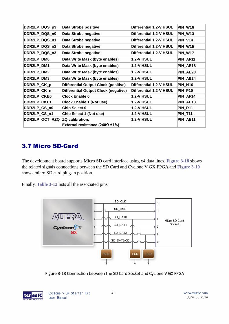
The development board supports Micro SD card interface using x4 data lines. Figure 3-18 shows
the related signals connections between the SD Card and Cyclone V GX FPGA and Figure 3-19
shows micro SD card plug-in position.
Finally, Table 3-12 lists all the associated pins
Figure 3-18 Connection between the SD Card Socket and Cyclone V GX FPGA
Cyclone V GX Starter Kit
User Manual
42
www.terasic.com
June 5, 2014
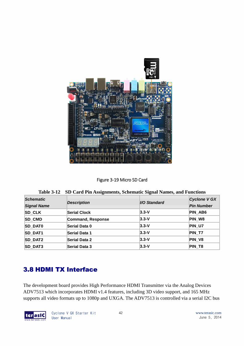
Figure 3-19 Micro SD Card
Table 3-12 SD Card Pin Assignments, Schematic Signal Names, and Functions
Schematic
Signal Name Description I/O Standard
Cyclone V GX
Pin Number
SD_CLK Serial Clock 3.3-V PIN_AB6
SD_CMD Command, Response 3.3-V PIN_W8
SD_DAT0 Serial Data 0 3.3-V PIN_U7
SD_DAT1 Serial Data 1 3.3-V PIN_T7
SD_DAT2 Serial Data 2 3.3-V PIN_V8
SD_DAT3 Serial Data 3 3.3-V PIN_T8
33..88 HHDDMMII TTXX IInntteerrffaaccee
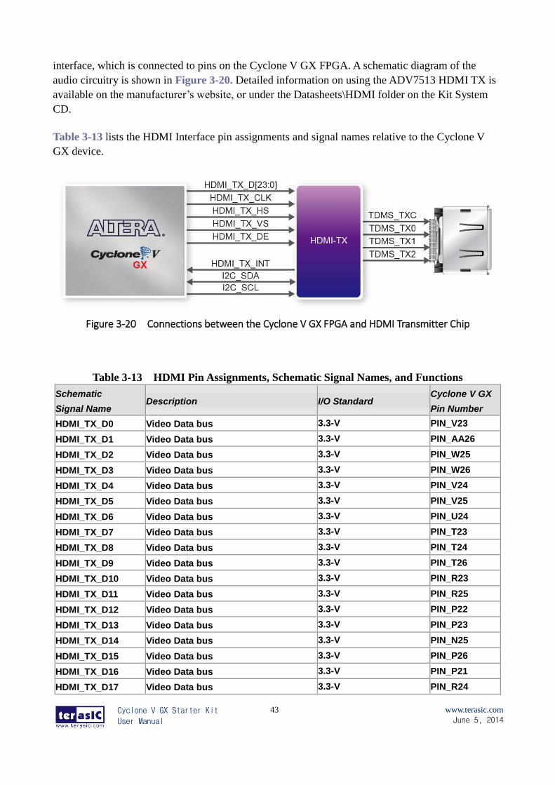
The development board provides High Performance HDMI Transmitter via the Analog Devices
ADV7513 which incorporates HDMI v1.4 features, including 3D video support, and 165 MHz
supports all video formats up to 1080p and UXGA. The ADV7513 is controlled via a serial I2C bus
Cyclone V GX Starter Kit
User Manual
43
www.terasic.com
June 5, 2014
interface, which is connected to pins on the Cyclone V GX FPGA. A schematic diagram of the
audio circuitry is shown in Figure 3-20. Detailed information on using the ADV7513 HDMI TX is
available on the manufacturer’s website, or under the Datasheets\HDMI folder on the Kit System
CD.
Table 3-13 lists the HDMI Interface pin assignments and signal names relative to the Cyclone V
GX device.
Figure 3-20 Connections between the Cyclone V GX FPGA and HDMI Transmitter Chip
Table 3-13 HDMI Pin Assignments, Schematic Signal Names, and Functions
Schematic
Signal Name Description I/O Standard
Cyclone V GX
Pin Number
HDMI_TX_D0 Video Data bus 3.3-V PIN_V23
HDMI_TX_D1 Video Data bus 3.3-V PIN_AA26
HDMI_TX_D2 Video Data bus 3.3-V PIN_W25
HDMI_TX_D3 Video Data bus 3.3-V PIN_W26
HDMI_TX_D4 Video Data bus 3.3-V PIN_V24
HDMI_TX_D5 Video Data bus 3.3-V PIN_V25
HDMI_TX_D6 Video Data bus 3.3-V PIN_U24
HDMI_TX_D7 Video Data bus 3.3-V PIN_T23
HDMI_TX_D8 Video Data bus 3.3-V PIN_T24
HDMI_TX_D9 Video Data bus 3.3-V PIN_T26
HDMI_TX_D10 Video Data bus 3.3-V PIN_R23
HDMI_TX_D11 Video Data bus 3.3-V PIN_R25
HDMI_TX_D12 Video Data bus 3.3-V PIN_P22
HDMI_TX_D13 Video Data bus 3.3-V PIN_P23
HDMI_TX_D14 Video Data bus 3.3-V PIN_N25
HDMI_TX_D15 Video Data bus 3.3-V PIN_P26
HDMI_TX_D16 Video Data bus 3.3-V PIN_P21
HDMI_TX_D17 Video Data bus 3.3-V PIN_R24
Cyclone V GX Starter Kit
User Manual
44
www.terasic.com
June 5, 2014
HDMI_TX_D18 Video Data bus 3.3-V PIN_R26
HDMI_TX_D19 Video Data bus 3.3-V PIN_AB26
HDMI_TX_D20 Video Data bus 3.3-V PIN_AA24
HDMI_TX_D21 Video Data bus 3.3-V PIN_AB25
HDMI_TX_D22 Video Data bus 3.3-V PIN_AC25
HDMI_TX_D23 Video Data bus 3.3-V PIN_AD25
HDMI_TX_CLK Video Clock 3.3-V PIN_Y25
HDMI_TX_DE Data Enable Signal for Digital Video. 3.3-V PIN_Y26
HDMI_TX_HS Horizontal Synchronization 3.3-V PIN_U26
HDMI_TX_VS Vertical Synchronization 3.3-V PIN_U25
HDMI_TX_INT Interrupt Signal 1.2-V PIN_T12
I2C_SCL I2C Clock 2.5-V PIN_B7
I2C_SDA I2C Data 2.5-V PIN_G11
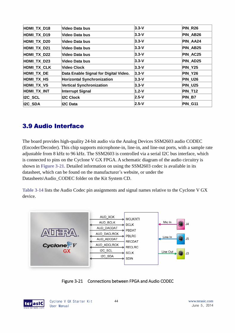
33..99 AAuuddiioo IInntteerrffaaccee
The board provides high-quality 24-bit audio via the Analog Devices SSM2603 audio CODEC
(Encoder/Decoder). This chip supports microphone-in, line-in, and line-out ports, with a sample rate
adjustable from 8 kHz to 96 kHz. The SSM2603 is controlled via a serial I2C bus interface, which
is connected to pins on the Cyclone V GX FPGA. A schematic diagram of the audio circuitry is
shown in Figure 3-21. Detailed information on using the SSM2603 codec is available in its
datasheet, which can be found on the manufacturer’s website, or under the
Datasheets\Audio_CODEC folder on the Kit System CD.
Table 3-14 lists the Audio Codec pin assignments and signal names relative to the Cyclone V GX
device.
Figure 3-21 Connections between FPGA and Audio CODEC
Cyclone V GX Starter Kit
User Manual
45
www.terasic.com
June 5, 2014
Table 3-14 Audio CODEC Pin Assignments, Schematic Signal Names, and Functions
Schematic
Signal Name Description I/O Standard
Cyclone V GX
Pin Number
AUD_ADCLRCK Audio CODEC ADC LR Clock 2.5-V PIN_C7
AUD_ADCDAT Audio CODEC ADC Data 2.5-V PIN_D7
AUD_DACLRCK Audio CODEC DAC LR Clock 2.5-V PIN_G10
AUD_DACDAT Audio CODEC DAC Data 2.5-V PIN_H10
AUD_XCK Audio CODEC Chip Clock 2.5-V PIN_D6
AUD_BCLK Audio CODEC Bit-Stream Clock 2.5-V PIN_E6
I2C_SCL I2C Clock 2.5-V PIN_B7
I2C_SDA I2C Data 2.5-V PIN_G11
33..1100 HHSSMMCC :: HHiigghh--SSppeeeedd MMeezzzzaanniinnee CCaarrdd
The FPGA development board has one HSMC connector. The HSMC connector provides a
mechanism to extend the peripheral-set of a FPGA host board by means of add-on cards, which can
address today’s high speed signaling requirement as well as low-speed device interface support. The
HSMC interfaces support JTAG, clock outputs and inputs, high-speed serial I/O (transceivers), and
single-ended or differential signaling.
The HSMC interface connected to the Cyclone V GX device is a female HSMC connector having a
total of 172pins, including 121 signal pins (120 signal pins +1 PSNTn pin), 39 power pins, and 12
ground pins. The HSMC connector is based on the SAMTEC 0.5 mm pitch, surface-mount QSH
family of high-speed, board-to-board connectors. The Cyclone V GX device provides +12 V DC
and +3.3 V DC power to the mezzanine card through the HSMC connector. Table 3-15 indicates the
maximum power consumption for the HSMC connector.
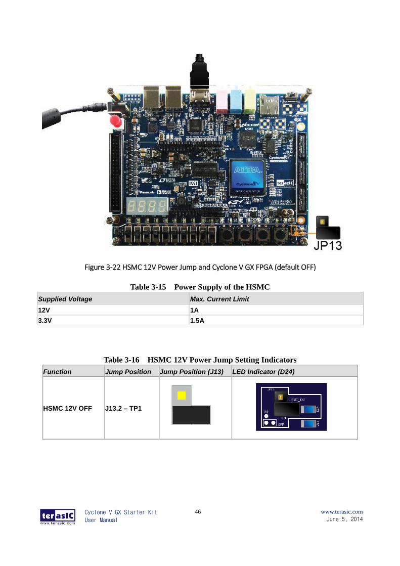
Note that the +12V DC power rail goes through a jumper (See Figure 3-22). The function of the
jumper is to avoid cases when users no longer use the 12V power, and the power goes directly to
HSMC daughter boards and thus leads to burning the FPGA I/Os.
This jumper can be found bottom-right corner near the HSMC connector. The factory default setting
is "OFF", meaning the 12V power won't be available to the daughter boards. When users need to
connect the daughter boards, they need to switch the jumper to "ON" position. Please see Table
3-16 for setting details.
Cyclone V GX Starter Kit
User Manual
46
www.terasic.com
June 5, 2014
Figure 3-22 HSMC 12V Power Jump and Cyclone V GX FPGA (default OFF)
Table 3-15 Power Supply of the HSMC
Supplied Voltage Max. Current Limit
12V 1A
3.3V 1.5A
Table 3-16 HSMC 12V Power Jump Setting Indicators
Function Jump Position Jump Position (J13) LED Indicator (D24)
HSMC 12V OFF J13.2 – TP1
Cyclone V GX Starter Kit
User Manual
47
www.terasic.com
June 5, 2014
HSMC 12V ON J13.1 – J13.2
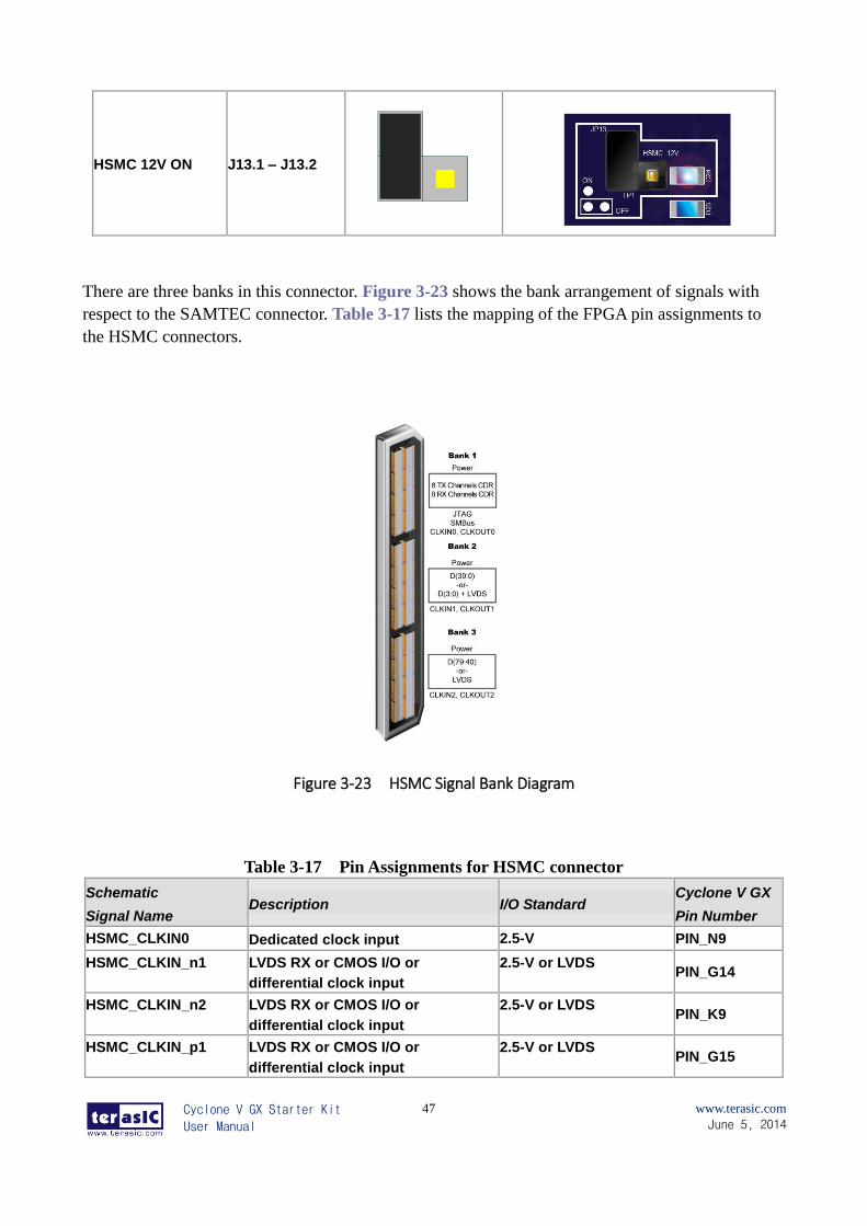
There are three banks in this connector. Figure 3-23 shows the bank arrangement of signals with
respect to the SAMTEC connector. Table 3-17 lists the mapping of the FPGA pin assignments to
the HSMC connectors.
Figure 3-23 HSMC Signal Bank Diagram
Table 3-17 Pin Assignments for HSMC connector
Schematic
Signal Name Description I/O Standard
Cyclone V GX
Pin Number
HSMC_CLKIN0 Dedicated clock input 2.5-V PIN_N9
HSMC_CLKIN_n1 LVDS RX or CMOS I/O or
differential clock input
2.5-V or LVDS PIN_G14
HSMC_CLKIN_n2 LVDS RX or CMOS I/O or
differential clock input
2.5-V or LVDS PIN_K9
HSMC_CLKIN_p1 LVDS RX or CMOS I/O or
differential clock input
2.5-V or LVDS PIN_G15
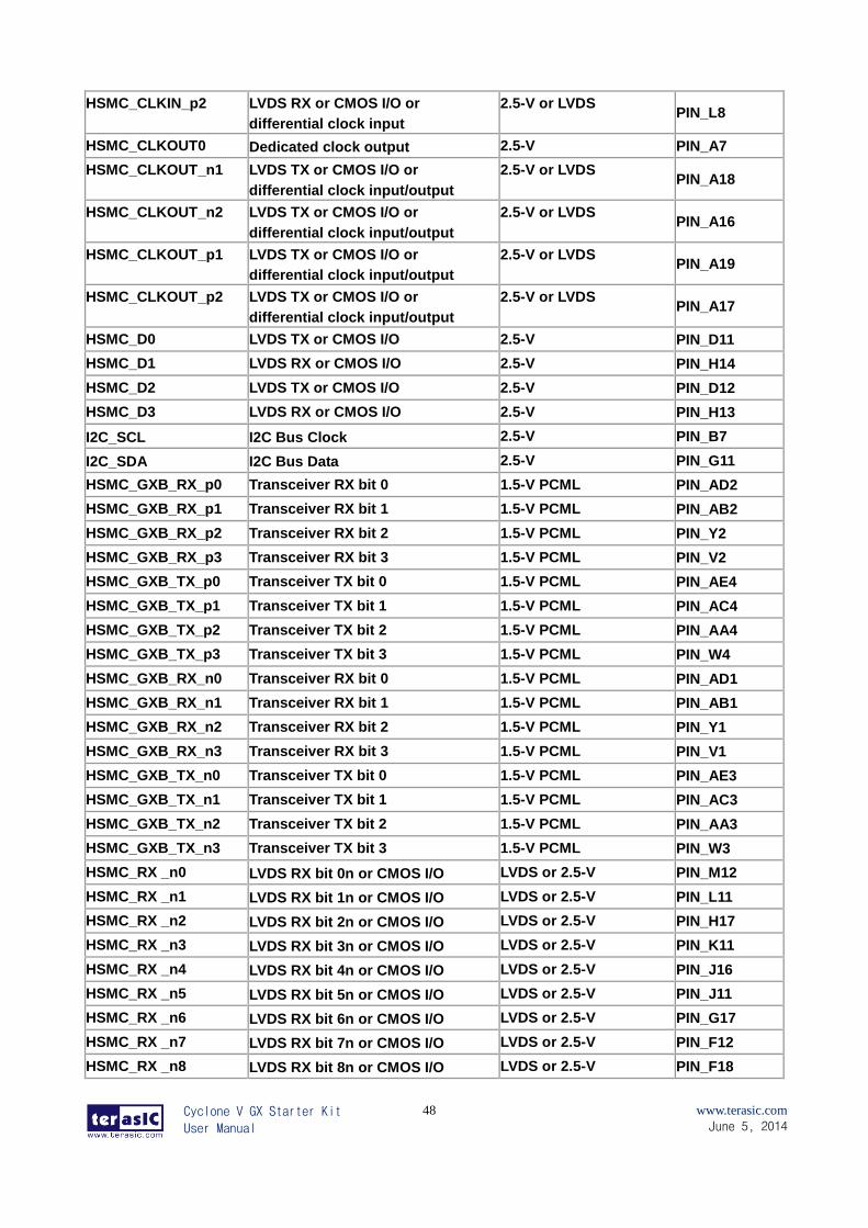
Cyclone V GX Starter Kit
User Manual
48
www.terasic.com
June 5, 2014
HSMC_CLKIN_p2 LVDS RX or CMOS I/O or
differential clock input
2.5-V or LVDS PIN_L8
HSMC_CLKOUT0 Dedicated clock output 2.5-V PIN_A7
HSMC_CLKOUT_n1 LVDS TX or CMOS I/O or
differential clock input/output
2.5-V or LVDS PIN_A18
HSMC_CLKOUT_n2 LVDS TX or CMOS I/O or
differential clock input/output
2.5-V or LVDS PIN_A16
HSMC_CLKOUT_p1 LVDS TX or CMOS I/O or
differential clock input/output
2.5-V or LVDS PIN_A19
HSMC_CLKOUT_p2 LVDS TX or CMOS I/O or
differential clock input/output
2.5-V or LVDS PIN_A17
HSMC_D0 LVDS TX or CMOS I/O 2.5-V PIN_D11
HSMC_D1 LVDS RX or CMOS I/O 2.5-V PIN_H14
HSMC_D2 LVDS TX or CMOS I/O 2.5-V PIN_D12
HSMC_D3 LVDS RX or CMOS I/O 2.5-V PIN_H13
I2C_SCL I2C Bus Clock 2.5-V PIN_B7
I2C_SDA I2C Bus Data 2.5-V PIN_G11
HSMC_GXB_RX_p0 Transceiver RX bit 0 1.5-V PCML PIN_AD2
HSMC_GXB_RX_p1 Transceiver RX bit 1 1.5-V PCML PIN_AB2
HSMC_GXB_RX_p2 Transceiver RX bit 2 1.5-V PCML PIN_Y2
HSMC_GXB_RX_p3 Transceiver RX bit 3 1.5-V PCML PIN_V2
HSMC_GXB_TX_p0 Transceiver TX bit 0 1.5-V PCML PIN_AE4
HSMC_GXB_TX_p1 Transceiver TX bit 1 1.5-V PCML PIN_AC4
HSMC_GXB_TX_p2 Transceiver TX bit 2 1.5-V PCML PIN_AA4
HSMC_GXB_TX_p3 Transceiver TX bit 3 1.5-V PCML PIN_W4
HSMC_GXB_RX_n0 Transceiver RX bit 0 1.5-V PCML PIN_AD1
HSMC_GXB_RX_n1 Transceiver RX bit 1 1.5-V PCML PIN_AB1
HSMC_GXB_RX_n2 Transceiver RX bit 2 1.5-V PCML PIN_Y1
HSMC_GXB_RX_n3 Transceiver RX bit 3 1.5-V PCML PIN_V1
HSMC_GXB_TX_n0 Transceiver TX bit 0 1.5-V PCML PIN_AE3
HSMC_GXB_TX_n1 Transceiver TX bit 1 1.5-V PCML PIN_AC3
HSMC_GXB_TX_n2 Transceiver TX bit 2 1.5-V PCML PIN_AA3
HSMC_GXB_TX_n3 Transceiver TX bit 3 1.5-V PCML PIN_W3
HSMC_RX _n0 LVDS RX bit 0n or CMOS I/O LVDS or 2.5-V PIN_M12
HSMC_RX _n1 LVDS RX bit 1n or CMOS I/O LVDS or 2.5-V PIN_L11
HSMC_RX _n2 LVDS RX bit 2n or CMOS I/O LVDS or 2.5-V PIN_H17
HSMC_RX _n3 LVDS RX bit 3n or CMOS I/O LVDS or 2.5-V PIN_K11
HSMC_RX _n4 LVDS RX bit 4n or CMOS I/O LVDS or 2.5-V PIN_J16
HSMC_RX _n5 LVDS RX bit 5n or CMOS I/O LVDS or 2.5-V PIN_J11
HSMC_RX _n6 LVDS RX bit 6n or CMOS I/O LVDS or 2.5-V PIN_G17
HSMC_RX _n7 LVDS RX bit 7n or CMOS I/O LVDS or 2.5-V PIN_F12
HSMC_RX _n8 LVDS RX bit 8n or CMOS I/O LVDS or 2.5-V PIN_F18
Cyclone V GX Starter Kit
User Manual
49
www.terasic.com
June 5, 2014
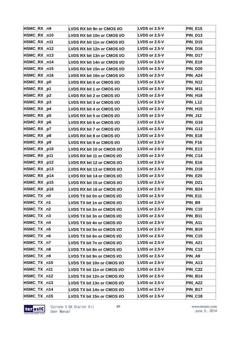
HSMC_RX _n9 LVDS RX bit 9n or CMOS I/O LVDS or 2.5-V PIN_E15
HSMC_RX _n10 LVDS RX bit 10n or CMOS I/O LVDS or 2.5-V PIN_D13
HSMC_RX _n11 LVDS RX bit 11n or CMOS I/O LVDS or 2.5-V PIN_D15
HSMC_RX _n12 LVDS RX bit 12n or CMOS I/O LVDS or 2.5-V PIN_D16
HSMC_RX _n13 LVDS RX bit 13n or CMOS I/O LVDS or 2.5-V PIN_D17
HSMC_RX _n14 LVDS RX bit 14n or CMOS I/O LVDS or 2.5-V PIN_E19
HSMC_RX _n15 LVDS RX bit 15n or CMOS I/O LVDS or 2.5-V PIN_D20
HSMC_RX _n16 LVDS RX bit 16n or CMOS I/O LVDS or 2.5-V PIN_A24
HSMC_RX _p0 LVDS RX bit 0 or CMOS I/O LVDS or 2.5-V PIN_N12
HSMC_RX _p1 LVDS RX bit 1 or CMOS I/O LVDS or 2.5-V PIN_M11
HSMC_RX _p2 LVDS RX bit 2 or CMOS I/O LVDS or 2.5-V PIN_H18
HSMC_RX _p3 LVDS RX bit 3 or CMOS I/O LVDS or 2.5-V PIN_L12
HSMC_RX _p4 LVDS RX bit 4 or CMOS I/O LVDS or 2.5-V PIN_H15
HSMC_RX _p5 LVDS RX bit 5 or CMOS I/O LVDS or 2.5-V PIN_J12
HSMC_RX _p6 LVDS RX bit 6 or CMOS I/O LVDS or 2.5-V PIN_G16
HSMC_RX _p7 LVDS RX bit 7 or CMOS I/O LVDS or 2.5-V PIN_G12
HSMC_RX _p8 LVDS RX bit 8 or CMOS I/O LVDS or 2.5-V PIN_E18
HSMC_RX _p9 LVDS RX bit 9 or CMOS I/O LVDS or 2.5-V PIN_F16
HSMC_RX _p10 LVDS RX bit 10 or CMOS I/O LVDS or 2.5-V PIN_E13
HSMC_RX _p11 LVDS RX bit 11 or CMOS I/O LVDS or 2.5-V PIN_C14
HSMC_RX _p12 LVDS RX bit 12 or CMOS I/O LVDS or 2.5-V PIN_E16
HSMC_RX _p13 LVDS RX bit 13 or CMOS I/O LVDS or 2.5-V PIN_D18
HSMC_RX _p14 LVDS RX bit 14 or CMOS I/O LVDS or 2.5-V PIN_E20
HSMC_RX _p15 LVDS RX bit 15 or CMOS I/O LVDS or 2.5-V PIN_D21
HSMC_RX _p16 LVDS RX bit 16 or CMOS I/O LVDS or 2.5-V PIN_B24
HSMC_TX _n0 LVDS TX bit 0n or CMOS I/O LVDS or 2.5-V PIN_E11
HSMC_TX _n1 LVDS TX bit 1n or CMOS I/O LVDS or 2.5-V PIN_B9
HSMC_TX _n2 LVDS TX bit 2n or CMOS I/O LVDS or 2.5-V PIN_C10
HSMC_TX _n3 LVDS TX bit 3n or CMOS I/O LVDS or 2.5-V PIN_B11
HSMC_TX _n4 LVDS TX bit 4n or CMOS I/O LVDS or 2.5-V PIN_A11
HSMC_TX _n5 LVDS TX bit 5n or CMOS I/O LVDS or 2.5-V PIN_B19
HSMC_TX _n6 LVDS TX bit 6n or CMOS I/O LVDS or 2.5-V PIN_C15
HSMC_TX _n7 LVDS TX bit 7n or CMOS I/O LVDS or 2.5-V PIN_A21
HSMC_TX _n8 LVDS TX bit 8n or CMOS I/O LVDS or 2.5-V PIN_C12
HSMC_TX _n9 LVDS TX bit 9n or CMOS I/O LVDS or 2.5-V PIN_A9
HSMC_TX _n10 LVDS TX bit 10n or CMOS I/O LVDS or 2.5-V PIN_A13
HSMC_TX _n11 LVDS TX bit 11n or CMOS I/O LVDS or 2.5-V PIN_C22
HSMC_TX _n12 LVDS TX bit 12n or CMOS I/O LVDS or 2.5-V PIN_B14
HSMC_TX _n13 LVDS TX bit 13n or CMOS I/O LVDS or 2.5-V PIN_A22
HSMC_TX _n14 LVDS TX bit 14n or CMOS I/O LVDS or 2.5-V PIN_B17
HSMC_TX _n15 LVDS TX bit 15n or CMOS I/O LVDS or 2.5-V PIN_C18
Cyclone V GX Starter Kit
User Manual
50
www.terasic.com
June 5, 2014
HSMC_TX _n16 LVDS TX bit 16n or CMOS I/O LVDS or 2.5-V PIN_B20
HSMC_TX _p0 LVDS TX bit 0 or CMOS I/O LVDS or 2.5-V PIN_E10
HSMC_TX _p1 LVDS TX bit 1 or CMOS I/O LVDS or 2.5-V PIN_C9
HSMC_TX _p2 LVDS TX bit 2 or CMOS I/O LVDS or 2.5-V PIN_D10
HSMC_TX _p3 LVDS TX bit 3 or CMOS I/O LVDS or 2.5-V PIN_A12
HSMC_TX _p4 LVDS TX bit 4 or CMOS I/O LVDS or 2.5-V PIN_B10
HSMC_TX _p5 LVDS TX bit 5 or CMOS I/O LVDS or 2.5-V PIN_C20
HSMC_TX _p6 LVDS TX bit 6 or CMOS I/O LVDS or 2.5-V PIN_B15
HSMC_TX _p7 LVDS TX bit 7 or CMOS I/O LVDS or 2.5-V PIN_B22
HSMC_TX _p8 LVDS TX bit 8 or CMOS I/O LVDS or 2.5-V PIN_C13
HSMC_TX _p9 LVDS TX bit 9 or CMOS I/O LVDS or 2.5-V PIN_A8
HSMC_TX _p10 LVDS TX bit 10 or CMOS I/O LVDS or 2.5-V PIN_B12
HSMC_TX _p11 LVDS TX bit 11 or CMOS I/O LVDS or 2.5-V PIN_C23
HSMC_TX _p12 LVDS TX bit 12 or CMOS I/O LVDS or 2.5-V PIN_A14
HSMC_TX _p13 LVDS TX bit 13 or CMOS I/O LVDS or 2.5-V PIN_A23
HSMC_TX _p14 LVDS TX bit 14 or CMOS I/O LVDS or 2.5-V PIN_C17
HSMC_TX _p15 LVDS TX bit 15 or CMOS I/O LVDS or 2.5-V PIN_C19
HSMC_TX _p16 LVDS TX bit 16 or CMOS I/O LVDS or 2.5-V PIN_B21
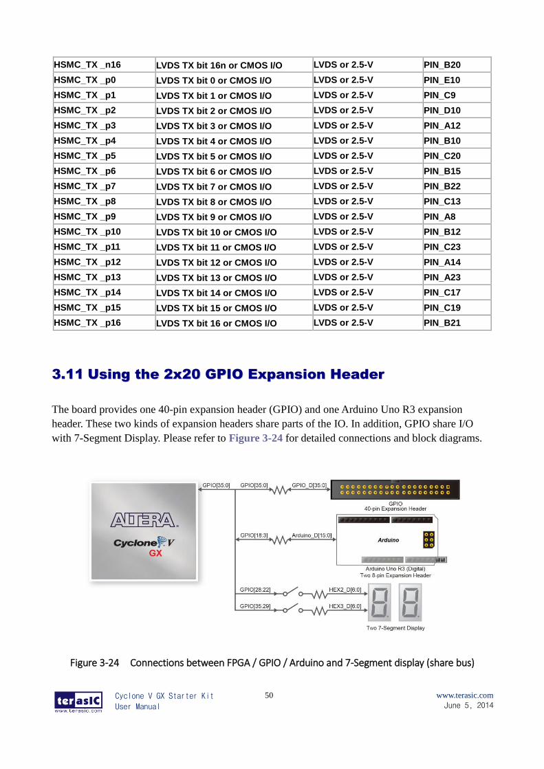
33..1111 UUssiinngg tthhee 22xx2200 GGPPIIOO EExxppaannssiioonn HHeeaaddeerr
The board provides one 40-pin expansion header (GPIO) and one Arduino Uno R3 expansion
header. These two kinds of expansion headers share parts of the IO. In addition, GPIO share I/O
with 7-Segment Display. Please refer to Figure 3-24 for detailed connections and block diagrams.
Figure 3-24 Connections between FPGA / GPIO / Arduino and 7-Segment display (share bus)
Cyclone V GX Starter Kit
User Manual
51
www.terasic.com
June 5, 2014
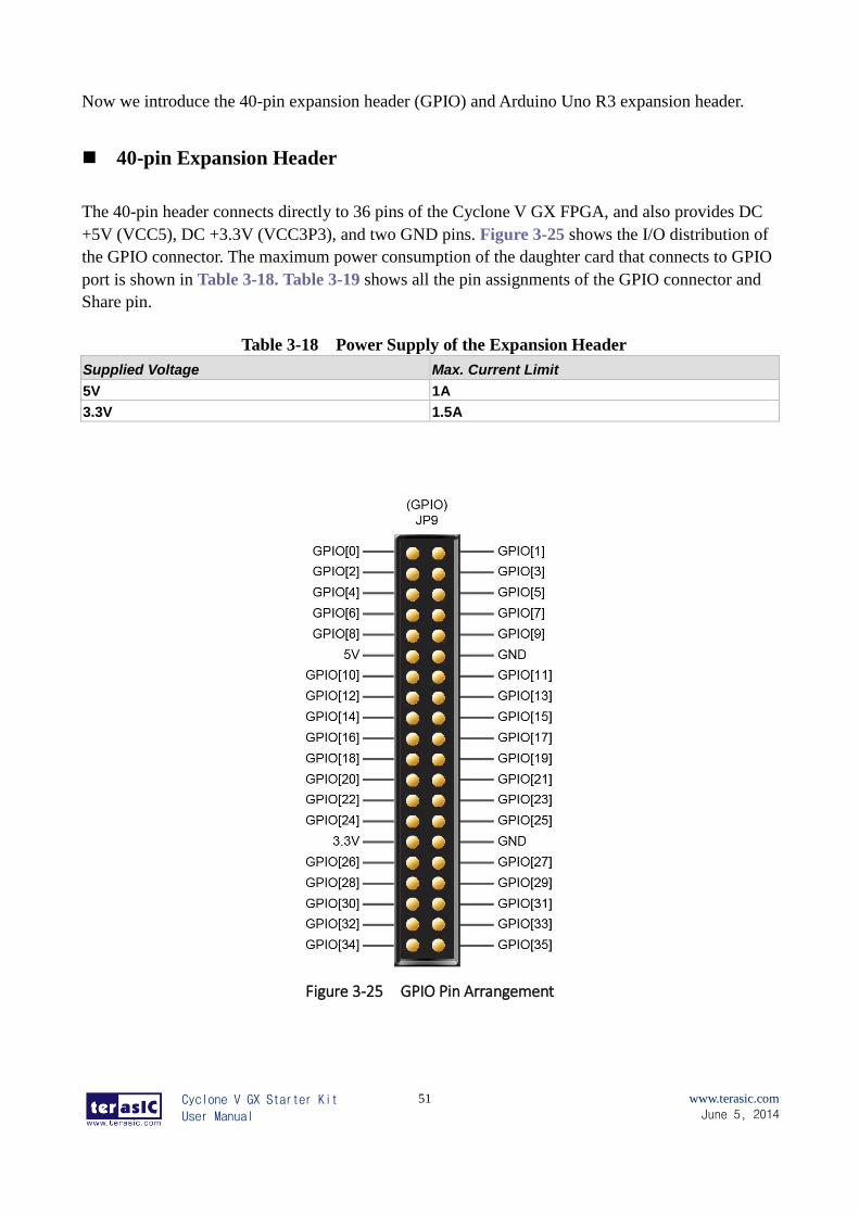
Now we introduce the 40-pin expansion header (GPIO) and Arduino Uno R3 expansion header.
40-pin Expansion Header
The 40-pin header connects directly to 36 pins of the Cyclone V GX FPGA, and also provides DC
+5V (VCC5), DC +3.3V (VCC3P3), and two GND pins. Figure 3-25 shows the I/O distribution of
the GPIO connector. The maximum power consumption of the daughter card that connects to GPIO
port is shown in Table 3-18. Table 3-19 shows all the pin assignments of the GPIO connector and
Share pin.
Table 3-18 Power Supply of the Expansion Header
Supplied Voltage Max. Current Limit
5V 1A
3.3V 1.5A
Figure 3-25 GPIO Pin Arrangement
Cyclone V GX Starter Kit
User Manual
52
www.terasic.com
June 5, 2014
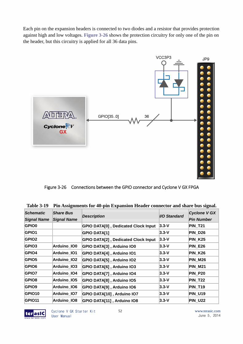
Each pin on the expansion headers is connected to two diodes and a resistor that provides protection
against high and low voltages. Figure 3-26 shows the protection circuitry for only one of the pin on
the header, but this circuitry is applied for all 36 data pins.
Figure 3-26 Connections between the GPIO connector and Cyclone V GX FPGA
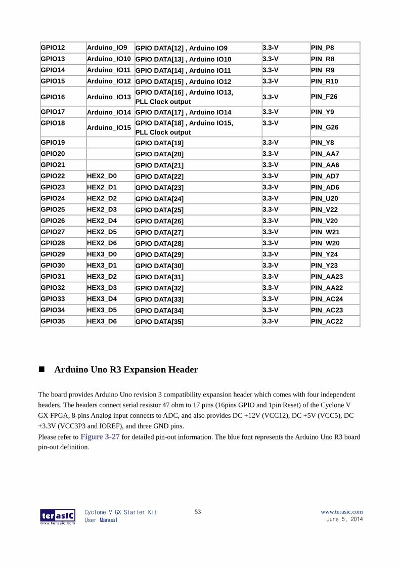
Table 3-19 Pin Assignments for 40-pin Expansion Header connector and share bus signal.
Schematic
Signal Name
Share Bus
Signal Name Description I/O Standard
Cyclone V GX
Pin Number
GPIO0 GPIO DATA[0] , Dedicated Clock Input 3.3-V PIN_T21
GPIO1 GPIO DATA[1] 3.3-V PIN_D26
GPIO2 GPIO DATA[2] , Dedicated Clock Input 3.3-V PIN_K25
GPIO3 Arduino_IO0 GPIO DATA[3] , Arduino IO0 3.3-V PIN_E26
GPIO4 Arduino_IO1 GPIO DATA[4] , Arduino IO1 3.3-V PIN_K26
GPIO5 Arduino_IO2 GPIO DATA[5] , Arduino IO2 3.3-V PIN_M26
GPIO6 Arduino_IO3 GPIO DATA[6] , Arduino IO3 3.3-V PIN_M21
GPIO7 Arduino_IO4 GPIO DATA[7] , Arduino IO4 3.3-V PIN_P20
GPIO8 Arduino_IO5 GPIO DATA[8] , Arduino IO5 3.3-V PIN_T22
GPIO9 Arduino_IO6 GPIO DATA[9] , Arduino IO6 3.3-V PIN_T19
GPIO10 Arduino_IO7 GPIO DATA[10] , Arduino IO7 3.3-V PIN_U19
GPIO11 Arduino_IO8 GPIO DATA[11] , Arduino IO8 3.3-V PIN_U22
Cyclone V GX Starter Kit
User Manual
53
www.terasic.com
June 5, 2014
GPIO12 Arduino_IO9 GPIO DATA[12] , Arduino IO9 3.3-V PIN_P8
GPIO13 Arduino_IO10 GPIO DATA[13] , Arduino IO10 3.3-V PIN_R8
GPIO14 Arduino_IO11 GPIO DATA[14] , Arduino IO11 3.3-V PIN_R9
GPIO15 Arduino_IO12 GPIO DATA[15] , Arduino IO12 3.3-V PIN_R10
GPIO16 Arduino_IO13 GPIO DATA[16] , Arduino IO13,
PLL Clock output 3.3-V PIN_F26
GPIO17 Arduino_IO14 GPIO DATA[17] , Arduino IO14 3.3-V PIN_Y9
GPIO18 Arduino_IO15
GPIO DATA[18] , Arduino IO15,
PLL Clock output
3.3-V PIN_G26
GPIO19 GPIO DATA[19] 3.3-V PIN_Y8
GPIO20 GPIO DATA[20] 3.3-V PIN_AA7
GPIO21 GPIO DATA[21] 3.3-V PIN_AA6
GPIO22 HEX2_D0 GPIO DATA[22] 3.3-V PIN_AD7
GPIO23 HEX2_D1 GPIO DATA[23] 3.3-V PIN_AD6
GPIO24 HEX2_D2 GPIO DATA[24] 3.3-V PIN_U20
GPIO25 HEX2_D3 GPIO DATA[25] 3.3-V PIN_V22
GPIO26 HEX2_D4 GPIO DATA[26] 3.3-V PIN_V20
GPIO27 HEX2_D5 GPIO DATA[27] 3.3-V PIN_W21
GPIO28 HEX2_D6 GPIO DATA[28] 3.3-V PIN_W20
GPIO29 HEX3_D0 GPIO DATA[29] 3.3-V PIN_Y24
GPIO30 HEX3_D1 GPIO DATA[30] 3.3-V PIN_Y23
GPIO31 HEX3_D2 GPIO DATA[31] 3.3-V PIN_AA23
GPIO32 HEX3_D3 GPIO DATA[32] 3.3-V PIN_AA22
GPIO33 HEX3_D4 GPIO DATA[33] 3.3-V PIN_AC24
GPIO34 HEX3_D5 GPIO DATA[34] 3.3-V PIN_AC23
GPIO35 HEX3_D6 GPIO DATA[35] 3.3-V PIN_AC22
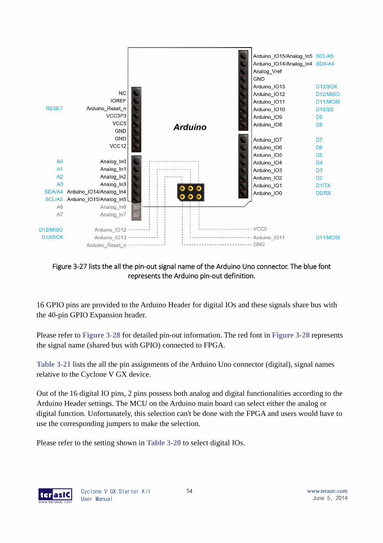
Arduino Uno R3 Expansion Header
The board provides Arduino Uno revision 3 compatibility expansion header which comes with four independent
headers. The headers connect serial resistor 47 ohm to 17 pins (16pins GPIO and 1pin Reset) of the Cyclone V
GX FPGA, 8-pins Analog input connects to ADC, and also provides DC +12V (VCC12), DC +5V (VCC5), DC
+3.3V (VCC3P3 and IOREF), and three GND pins.
Please refer to Figure 3-27 for detailed pin-out information. The blue font represents the Arduino Uno R3 board
pin-out definition.
Cyclone V GX Starter Kit
User Manual
54
www.terasic.com
June 5, 2014
Figure 3-27 lists the all the pin-out signal name of the Arduino Uno connector. The blue font represents the Arduino pin-out definition.
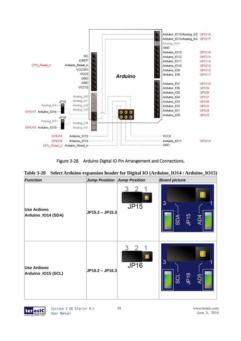
16 GPIO pins are provided to the Arduino Header for digital IOs and these signals share bus with
the 40-pin GPIO Expansion header.
Please refer to Figure 3-28 for detailed pin-out information. The red font in Figure 3-28 represents
the signal name (shared bus with GPIO) connected to FPGA.
Table 3-21 lists the all the pin assignments of the Arduino Uno connector (digital), signal names
relative to the Cyclone V GX device.
Out of the 16 digital IO pins, 2 pins possess both analog and digital functionalities according to the
Arduino Header settings. The MCU on the Arduino main board can select either the analog or
digital function. Unfortunately, this selection can't be done with the FPGA and users would have to
use the corresponding jumpers to make the selection.
Please refer to the setting shown in Table 3-20 to select digital IOs.
Cyclone V GX Starter Kit
User Manual
55
www.terasic.com
June 5, 2014
Figure 3-28 Arduino Digital IO Pin Arrangement and Connections.
Table 3-20 Select Arduino expansion header for Digital IO (Arduino_IO14 / Arduino_IO15)
Function Jump Position Jump Position Board picture
Use Ardiono
Arduino_IO14 (SDA) JP15.2 – JP15.3
Use Ardiono
Arduino_IO15 (SCL) JP16.2 – JP16.3
Cyclone V GX Starter Kit
User Manual
56
www.terasic.com
June 5, 2014
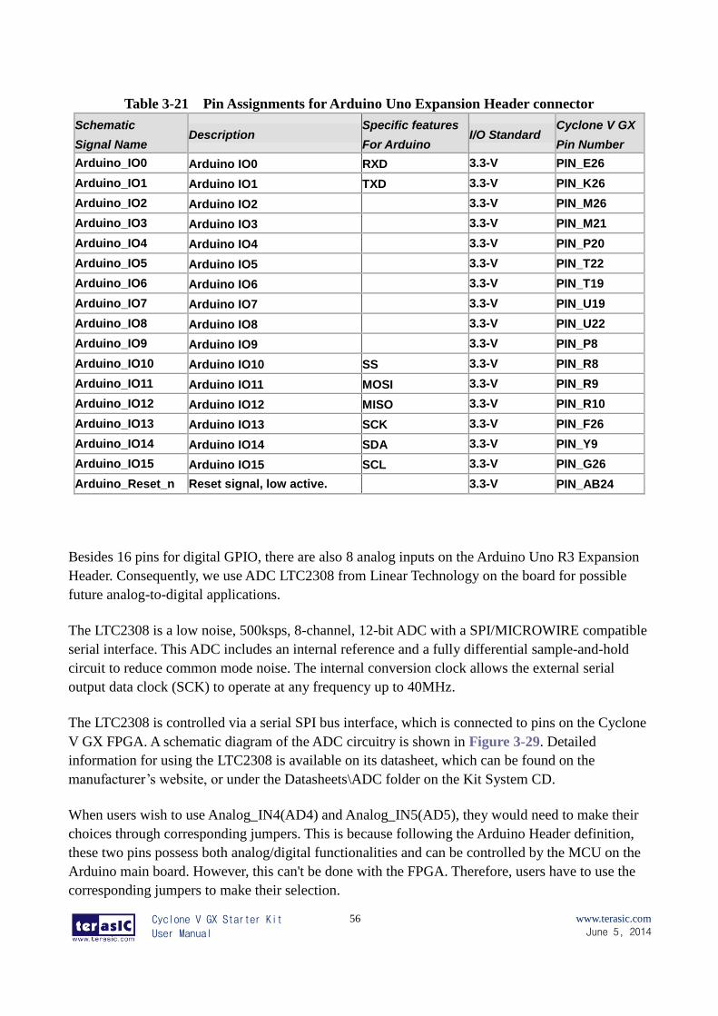
Table 3-21 Pin Assignments for Arduino Uno Expansion Header connector
Schematic
Signal Name Description
Specific features
For Arduino I/O Standard
Cyclone V GX
Pin Number
Arduino_IO0 Arduino IO0 RXD 3.3-V PIN_E26
Arduino_IO1 Arduino IO1 TXD 3.3-V PIN_K26
Arduino_IO2 Arduino IO2 3.3-V PIN_M26
Arduino_IO3 Arduino IO3 3.3-V PIN_M21
Arduino_IO4 Arduino IO4 3.3-V PIN_P20
Arduino_IO5 Arduino IO5 3.3-V PIN_T22
Arduino_IO6 Arduino IO6 3.3-V PIN_T19
Arduino_IO7 Arduino IO7 3.3-V PIN_U19
Arduino_IO8 Arduino IO8 3.3-V PIN_U22
Arduino_IO9 Arduino IO9 3.3-V PIN_P8
Arduino_IO10 Arduino IO10 SS 3.3-V PIN_R8
Arduino_IO11 Arduino IO11 MOSI 3.3-V PIN_R9
Arduino_IO12 Arduino IO12 MISO 3.3-V PIN_R10
Arduino_IO13 Arduino IO13 SCK 3.3-V PIN_F26
Arduino_IO14 Arduino IO14 SDA 3.3-V PIN_Y9
Arduino_IO15 Arduino IO15 SCL 3.3-V PIN_G26
Arduino_Reset_n Reset signal, low active. 3.3-V PIN_AB24
Besides 16 pins for digital GPIO, there are also 8 analog inputs on the Arduino Uno R3 Expansion
Header. Consequently, we use ADC LTC2308 from Linear Technology on the board for possible
future analog-to-digital applications.
The LTC2308 is a low noise, 500ksps, 8-channel, 12-bit ADC with a SPI/MICROWIRE compatible
serial interface. This ADC includes an internal reference and a fully differential sample-and-hold
circuit to reduce common mode noise. The internal conversion clock allows the external serial
output data clock (SCK) to operate at any frequency up to 40MHz.
The LTC2308 is controlled via a serial SPI bus interface, which is connected to pins on the Cyclone
V GX FPGA. A schematic diagram of the ADC circuitry is shown in Figure 3-29. Detailed
information for using the LTC2308 is available on its datasheet, which can be found on the
manufacturer’s website, or under the Datasheets\ADC folder on the Kit System CD.
When users wish to use Analog_IN4(AD4) and Analog_IN5(AD5), they would need to make their
choices through corresponding jumpers. This is because following the Arduino Header definition,
these two pins possess both analog/digital functionalities and can be controlled by the MCU on the
Arduino main board. However, this can't be done with the FPGA. Therefore, users have to use the
corresponding jumpers to make their selection.
Cyclone V GX Starter Kit
User Manual
57
www.terasic.com
June 5, 2014
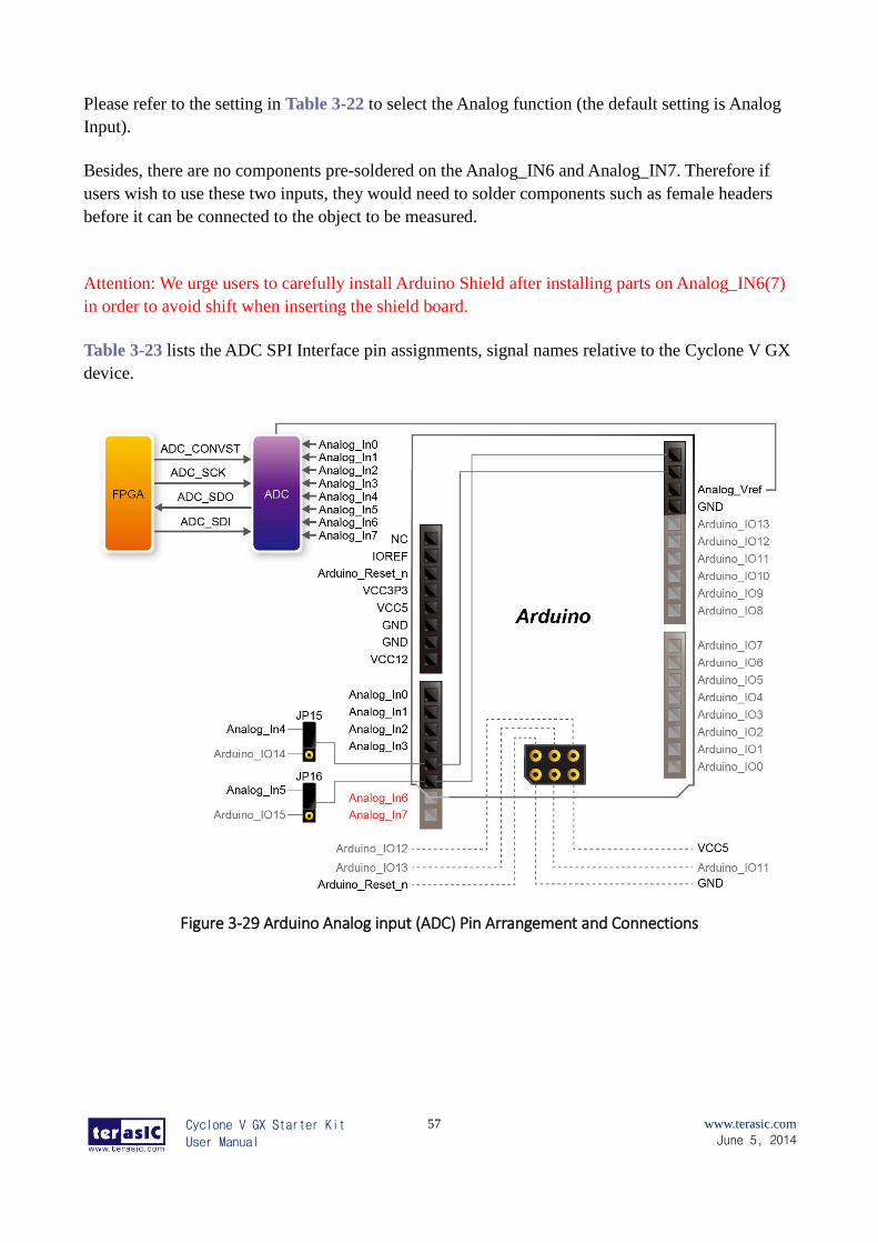
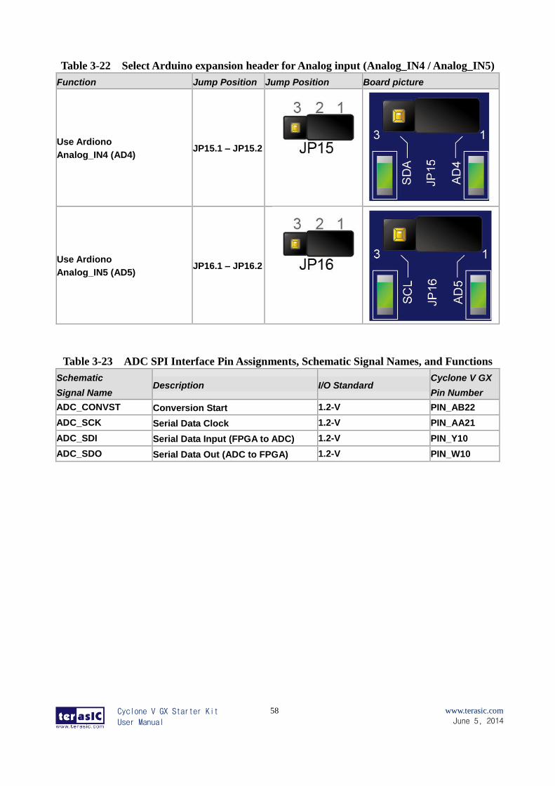
Please refer to the setting in Table 3-22 to select the Analog function (the default setting is Analog
Input).
Besides, there are no components pre-soldered on the Analog_IN6 and Analog_IN7. Therefore if
users wish to use these two inputs, they would need to solder components such as female headers
before it can be connected to the object to be measured.
Attention: We urge users to carefully install Arduino Shield after installing parts on Analog_IN6(7)
in order to avoid shift when inserting the shield board.
Table 3-23 lists the ADC SPI Interface pin assignments, signal names relative to the Cyclone V GX
device.
Figure 3-29 Arduino Analog input (ADC) Pin Arrangement and Connections
Cyclone V GX Starter Kit
User Manual
58
www.terasic.com
June 5, 2014
Table 3-22 Select Arduino expansion header for Analog input (Analog_IN4 / Analog_IN5)
Function Jump Position Jump Position Board picture
Use Ardiono
Analog_IN4 (AD4) JP15.1 – JP15.2
Use Ardiono
Analog_IN5 (AD5) JP16.1 – JP16.2
Table 3-23 ADC SPI Interface Pin Assignments, Schematic Signal Names, and Functions
Schematic
Signal Name Description I/O Standard
Cyclone V GX
Pin Number
ADC_CONVST Conversion Start 1.2-V PIN_AB22
ADC_SCK Serial Data Clock 1.2-V PIN_AA21
ADC_SDI Serial Data Input (FPGA to ADC) 1.2-V PIN_Y10
ADC_SDO Serial Data Out (ADC to FPGA) 1.2-V PIN_W10
Cyclone V GX Starter Kit
User Manual
59
www.terasic.com
June 5, 2014
Chapter 4
System Builder
This chapter describes how users can create a custom design project on the board by using the
Software Tool of Cyclone V GX Starter Kit – C5G System Builder.
44..11 IInnttrroodduuccttiioonn
The C5G System Builder is a Windows-based software utility, designed to assist users to create a
Quartus II project for the board within minutes. The generated Quartus II project files include:
Quartus II Project File (.qpf)
Quartus II Setting File (.qsf)
Top-Level Design File (.v)
Synopsis Design Constraints file (.sdc)
Pin Assignment Document (.htm)
By providing the above files, the C5G System Builder prevents occurrence of situations that are
prone to errors when users manually edit the top-level design file or place pin assignments. The
common mistakes that users encounter are the following:
1. Board damage due to wrong pin/bank voltage assignments.
2. Board malfunction caused by wrong device connections or missing pin counts for
connected ends.
3. Performance degradation due to improper pin assignments.
44..22 GGeenneerraall DDeessiiggnn FFllooww
This section will introduce the general design flow to build a project for the development board via
the C5G System Builder. The general design flow is illustrated in Figure 4-1.
Users should launch the C5G System Builder and create a new project according to their design
requirements. When users complete the settings, the C5G System Builder will generate two major
files, a top-level design file (.v) and a Quartus II setting file (.qsf).
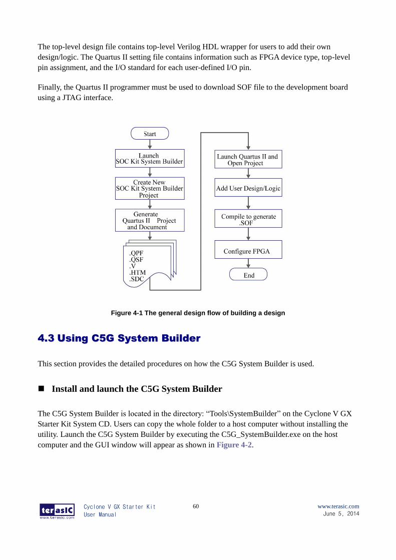
Cyclone V GX Starter Kit
User Manual
60
www.terasic.com
June 5, 2014
The top-level design file contains top-level Verilog HDL wrapper for users to add their own
design/logic. The Quartus II setting file contains information such as FPGA device type, top-level
pin assignment, and the I/O standard for each user-defined I/O pin.
Finally, the Quartus II programmer must be used to download SOF file to the development board
using a JTAG interface.
Figure 4-1 The general design flow of building a design
44..33 UUssiinngg CC55GG SSyysstteemm BBuuiillddeerr
This section provides the detailed procedures on how the C5G System Builder is used.
Install and launch the C5G System Builder
The C5G System Builder is located in the directory: “Tools\SystemBuilder” on the Cyclone V GX
Starter Kit System CD. Users can copy the whole folder to a host computer without installing the
utility. Launch the C5G System Builder by executing the C5G_SystemBuilder.exe on the host
computer and the GUI window will appear as shown in Figure 4-2.
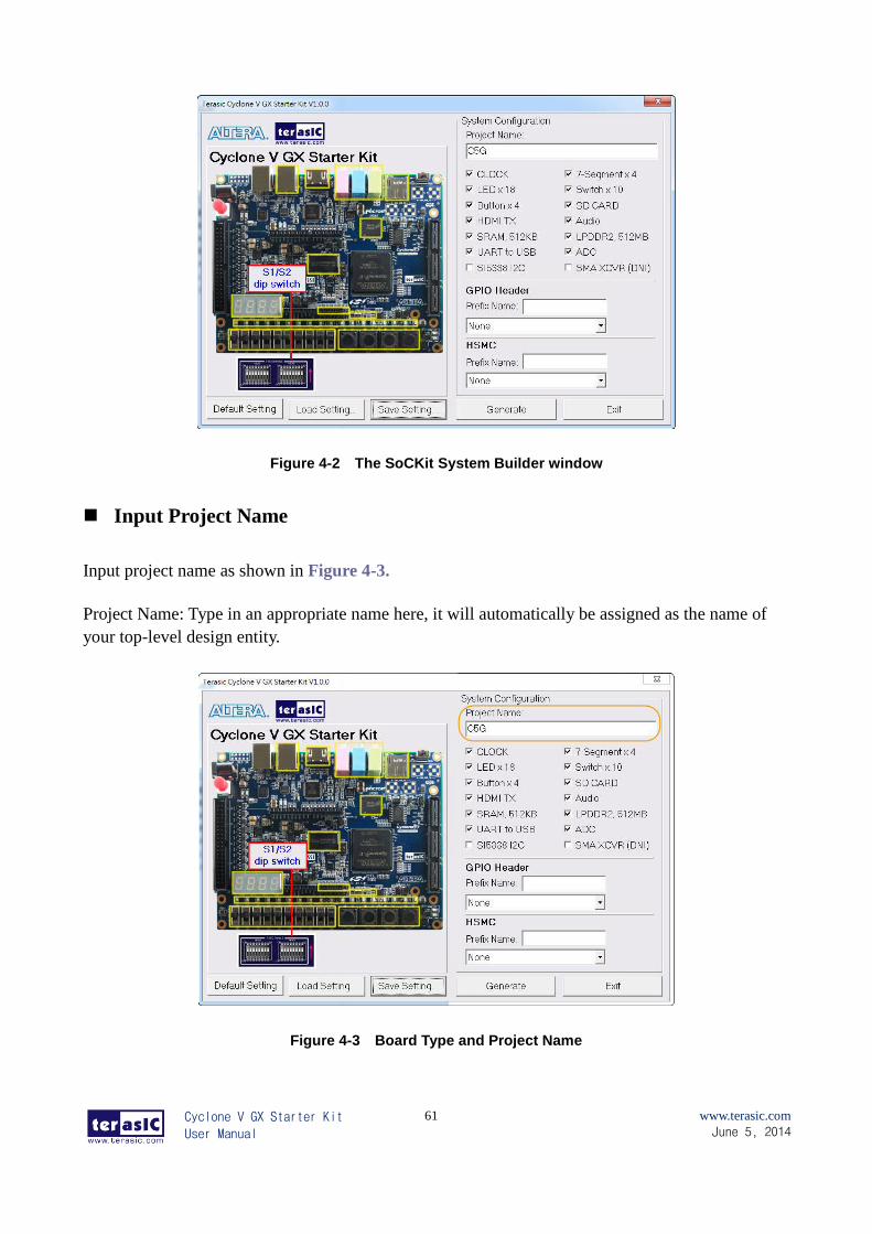
Cyclone V GX Starter Kit
User Manual
61
www.terasic.com
June 5, 2014
Figure 4-2 The SoCKit System Builder window
Input Project Name
Input project name as shown in Figure 4-3.
Project Name: Type in an appropriate name here, it will automatically be assigned as the name of
your top-level design entity.
Figure 4-3 Board Type and Project Name
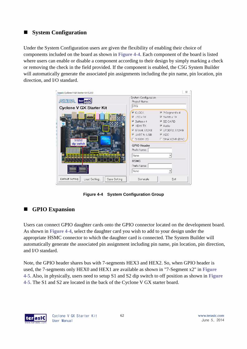
Cyclone V GX Starter Kit
User Manual
62
www.terasic.com
June 5, 2014
System Configuration
Under the System Configuration users are given the flexibility of enabling their choice of
components included on the board as shown in Figure 4-4. Each component of the board is listed
where users can enable or disable a component according to their design by simply marking a check
or removing the check in the field provided. If the component is enabled, the C5G System Builder
will automatically generate the associated pin assignments including the pin name, pin location, pin
direction, and I/O standard.
Figure 4-4 System Configuration Group
GPIO Expansion
Users can connect GPIO daughter cards onto the GPIO connector located on the development board.
As shown in Figure 4-4, select the daughter card you wish to add to your design under the
appropriate HSMC connector to which the daughter card is connected. The System Builder will
automatically generate the associated pin assignment including pin name, pin location, pin direction,
and I/O standard.
Note, the GPIO header shares bus with 7-segments HEX3 and HEX2. So, when GPIO header is
used, the 7-segments only HEX0 and HEX1 are available as shown in "7-Segment x2" in Figure
4-5. Also, in physically, users need to setup S1 and S2 dip switch to off position as shown in Figure
4-5. The S1 and S2 are located in the back of the Cyclone V GX starter board.
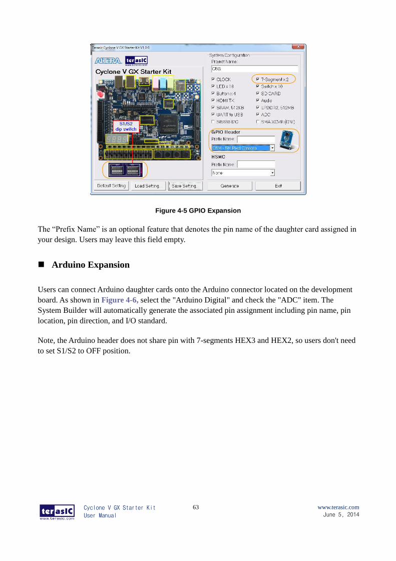
Cyclone V GX Starter Kit
User Manual
63
www.terasic.com
June 5, 2014
Figure 4-5 GPIO Expansion
The “Prefix Name” is an optional feature that denotes the pin name of the daughter card assigned in
your design. Users may leave this field empty.
Arduino Expansion
Users can connect Arduino daughter cards onto the Arduino connector located on the development
board. As shown in Figure 4-6, select the "Arduino Digital" and check the "ADC" item. The
System Builder will automatically generate the associated pin assignment including pin name, pin
location, pin direction, and I/O standard.
Note, the Arduino header does not share pin with 7-segments HEX3 and HEX2, so users don't need
to set S1/S2 to OFF position.
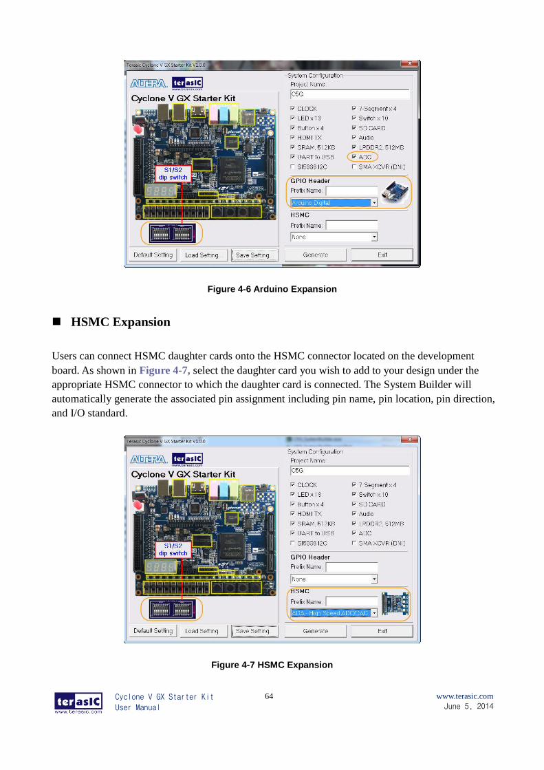
Cyclone V GX Starter Kit
User Manual
64
www.terasic.com
June 5, 2014
Figure 4-6 Arduino Expansion
HSMC Expansion
Users can connect HSMC daughter cards onto the HSMC connector located on the development
board. As shown in Figure 4-7, select the daughter card you wish to add to your design under the
appropriate HSMC connector to which the daughter card is connected. The System Builder will
automatically generate the associated pin assignment including pin name, pin location, pin direction,
and I/O standard.
Figure 4-7 HSMC Expansion
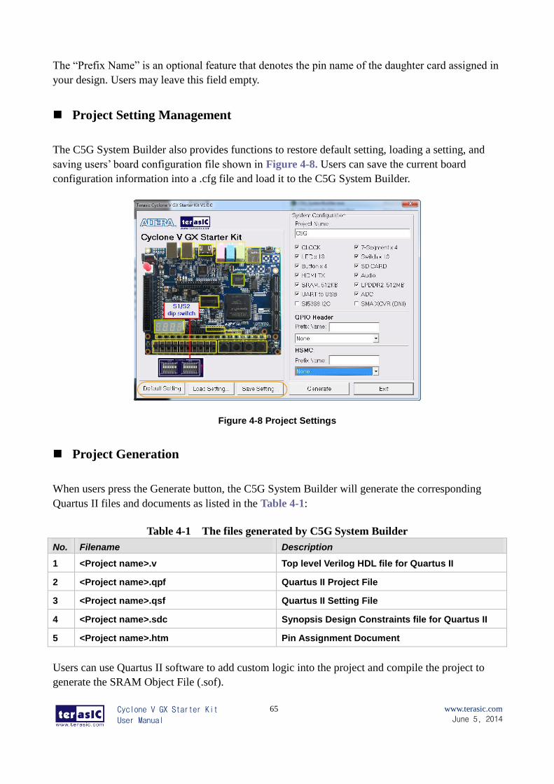
Cyclone V GX Starter Kit
User Manual
65
www.terasic.com
June 5, 2014
The “Prefix Name” is an optional feature that denotes the pin name of the daughter card assigned in
your design. Users may leave this field empty.
Project Setting Management
The C5G System Builder also provides functions to restore default setting, loading a setting, and
saving users’ board configuration file shown in Figure 4-8. Users can save the current board
configuration information into a .cfg file and load it to the C5G System Builder.
Figure 4-8 Project Settings
Project Generation
When users press the Generate button, the C5G System Builder will generate the corresponding
Quartus II files and documents as listed in the Table 4-1:
Table 4-1 The files generated by C5G System Builder
No. Filename Description
1 <Project name>.v Top level Verilog HDL file for Quartus II
2 <Project name>.qpf Quartus II Project File
3 <Project name>.qsf Quartus II Setting File
4 <Project name>.sdc Synopsis Design Constraints file for Quartus II
5 <Project name>.htm Pin Assignment Document
Users can use Quartus II software to add custom logic into the project and compile the project to
generate the SRAM Object File (.sof).
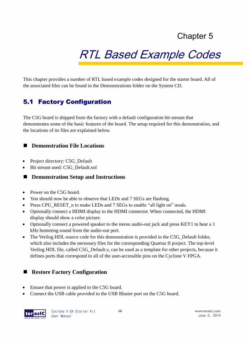
Cyclone V GX Starter Kit
User Manual
66
www.terasic.com
June 5, 2014
Chapter 5
RTL Based Example Codes
This chapter provides a number of RTL based example codes designed for the starter board. All of
the associated files can be found in the Demonstrations folder on the System CD.
55..11 FFaaccttoorryy CCoonnffiigguurraattiioonn
The C5G board is shipped from the factory with a default configuration bit-stream that
demonstrates some of the basic features of the board. The setup required for this demonstration, and
the locations of its files are explained below.
Demonstration File Locations
Project directory: C5G_Default
Bit stream used: C5G_Default.sof
Demonstration Setup and Instructions
Power on the C5G board.
You should now be able to observe that LEDs and 7 SEGs are flashing.
Press CPU_RESET_n to make LEDs and 7 SEGs to enable “all light on” mode.
Optionally connect a HDMI display to the HDMI connector. When connected, the HDMI
display should show a color picture.
Optionally connect a powered speaker to the stereo audio-out jack and press KEY1 to hear a 1
kHz humming sound from the audio-out port.
The Verilog HDL source code for this demonstration is provided in the C5G_Default folder,
which also includes the necessary files for the corresponding Quartus II project. The top-level
Verilog HDL file, called C5G_Default.v, can be used as a template for other projects, because it
defines ports that correspond to all of the user-accessible pins on the Cyclone V FPGA.
Restore Factory Configuration
Ensure that power is applied to the C5G board.
Connect the USB cable provided to the USB Blaster port on the C5G board.
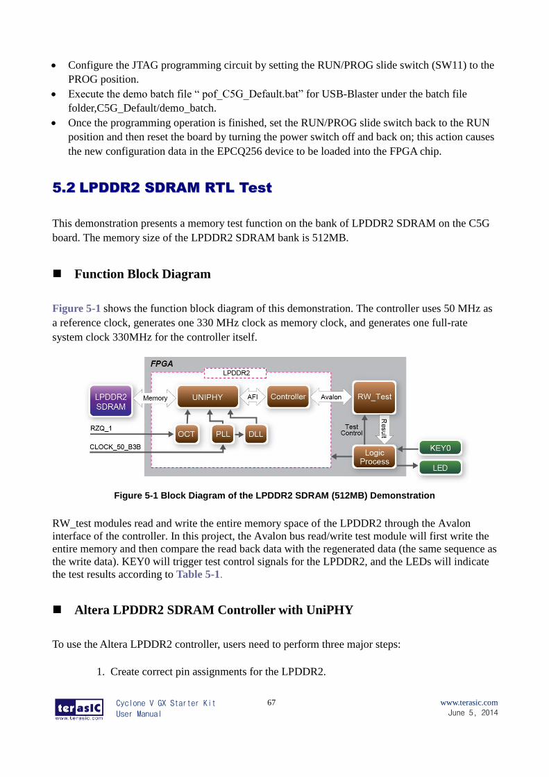
Cyclone V GX Starter Kit
User Manual
67
www.terasic.com
June 5, 2014
Configure the JTAG programming circuit by setting the RUN/PROG slide switch (SW11) to the
PROG position.
Execute the demo batch file “ pof_C5G_Default.bat” for USB-Blaster under the batch file
folder,C5G_Default/demo_batch.
Once the programming operation is finished, set the RUN/PROG slide switch back to the RUN
position and then reset the board by turning the power switch off and back on; this action causes
the new configuration data in the EPCQ256 device to be loaded into the FPGA chip.
55..22 LLPPDDDDRR22 SSDDRRAAMM RRTTLL TTeesstt
This demonstration presents a memory test function on the bank of LPDDR2 SDRAM on the C5G
board. The memory size of the LPDDR2 SDRAM bank is 512MB.
Function Block Diagram
Figure 5-1 shows the function block diagram of this demonstration. The controller uses 50 MHz as
a reference clock, generates one 330 MHz clock as memory clock, and generates one full-rate
system clock 330MHz for the controller itself.
Figure 5-1 Block Diagram of the LPDDR2 SDRAM (512MB) Demonstration
RW_test modules read and write the entire memory space of the LPDDR2 through the Avalon
interface of the controller. In this project, the Avalon bus read/write test module will first write the
entire memory and then compare the read back data with the regenerated data (the same sequence as
the write data). KEY0 will trigger test control signals for the LPDDR2, and the LEDs will indicate
the test results according to Table 5-1.
Altera LPDDR2 SDRAM Controller with UniPHY
To use the Altera LPDDR2 controller, users need to perform three major steps:
1. Create correct pin assignments for the LPDDR2.
Cyclone V GX Starter Kit
User Manual
68
www.terasic.com
June 5, 2014
2. Setup correct parameters in LPDDR2 controller dialog.
3. Perform “Analysis and Synthesis” by selecting from the Quartus II menu:
ProcessStartStart Analysis & Synthesis.
4. Run the TCL files generated by LPDDR2 IP by selecting from the Quartus II menu:
ToolsTCL Scripts…
Design Tools
64-Bit Quartus 13.1
Demonstration Source Code
Project directory: C5G_LPDDR2_RTL_Test
Bit stream used: C5G_LPDDR2_RTL_Test.sof
Demonstration Batch File
Demo Batch File Folder: C5G_LPDDR2_RTL_Test \demo_batch
The demo batch file includes following files:
Batch File: C5G_LPDDR2_RTL_Test.bat
FPGA Configure File: C5G_LPDDR2_RTL_Test.sof
Demonstration Setup
Make sure Quartus II is installed on your PC.
Connect the USB cable to the USB Blaster connector (J10) on the C5G board and host PC.
Power on the C5G board.
Execute the demo batch file “ C5G_LPDDR2_RTL_Test.bat” under the batch file folder,
C5G_LPDDR2_RTL_Test \demo_batch.
Press KEY0 on the C5G board to start the verification process. When KEY0 is pressed, the
LEDs (LEDG [2:0]) should turn on. At the instant of releasing KEY0, LEDG1, LEDG2 should
start blinking. After approximately 25 seconds, LEDG1 should stop blinking and stay on to
indicate that the LPDDR2 has passed the test, respectively. Table 5-1 lists the LED indicators.
If LEDG2 is not blinking, it means 50MHz clock source is not working.
If LEDG1 does not start blinking after releasing KEY0, it indicates local_init_done or
local_cal_success of the corresponding LPDDR2 failed.
If LEDG1 fails to remain on after 25 seconds, the corresponding LPDDR2 test has failed.
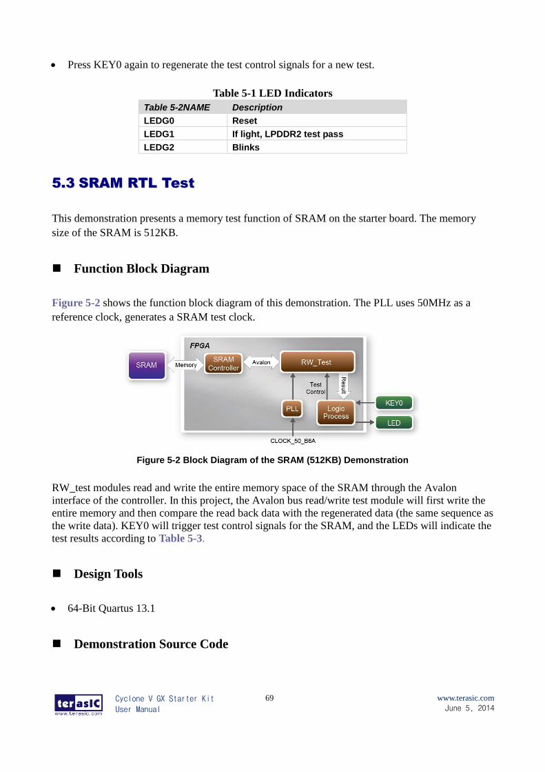
Cyclone V GX Starter Kit
User Manual
69
www.terasic.com
June 5, 2014
Press KEY0 again to regenerate the test control signals for a new test.
Table 5-1 LED Indicators
Table 5-2NAME Description
LEDG0 Reset
LEDG1 If light, LPDDR2 test pass
LEDG2 Blinks
55..33 SSRRAAMM RRTTLL TTeesstt
This demonstration presents a memory test function of SRAM on the starter board. The memory
size of the SRAM is 512KB.
Function Block Diagram
Figure 5-2 shows the function block diagram of this demonstration. The PLL uses 50MHz as a
reference clock, generates a SRAM test clock.
Figure 5-2 Block Diagram of the SRAM (512KB) Demonstration
RW_test modules read and write the entire memory space of the SRAM through the Avalon
interface of the controller. In this project, the Avalon bus read/write test module will first write the
entire memory and then compare the read back data with the regenerated data (the same sequence as
the write data). KEY0 will trigger test control signals for the SRAM, and the LEDs will indicate the
test results according to Table 5-3.
Design Tools
64-Bit Quartus 13.1
Demonstration Source Code
Cyclone V GX Starter Kit
User Manual
70
www.terasic.com
June 5, 2014
Project directory: C5G_SRAM_RTL_Test
Bit stream used: C5G_SRAM_RTL_Test.sof
Demonstration Batch File
Demo Batch File Folder: C5G_SRAM_RTL_Test \demo_batch
The demo batch file includes following files:
Batch File: C5G_SRAM_RTL_Test.bat
FPGA Configure File: C5G_SRAM_RTL_Test.sof
Demonstration Setup
Make sure Quartus II is installed on your PC.
Connect the USB cable to the USB Blaster connector (J10) on the C5G board and host PC.
Power on the C5G board.
Execute the demo batch file “ C5G_SRAM_RTL_Test.bat” under the batch file folder,
C5G_SRAM_RTL_Test \demo_batch.
Press KEY0 on the C5G board to start the verification process. When KEY0 is pressed, the
LEDs (LEDG [2:0]) should turn on. At the instant of releasing KEY0, LEDG1, LEDG2 should
start blinking. After approximately 4 seconds, LEDG1 should stop blinking and stay on to
indicate that the SRAM has passed the test, respectively. Table 5-3 lists the LED indicators.
If LEDG2 is not blinking, it means 50MHz clock source is not working.
If LEDG1 does not start blinking after releasing KEY0, it indicates local_init_done or
local_cal_success of the corresponding SRAM failed.
If LEDG1 fails to remain on after 4 seconds, the corresponding SRAM test has failed.
Press KEY0 again to regenerate the test control signals for a new test.
Table 5-3 LED Indicators
Table
5-4NAME Description
LEDG0 Reset
LEDG1 If light, SRAM test pass
LEDG2 Blinks
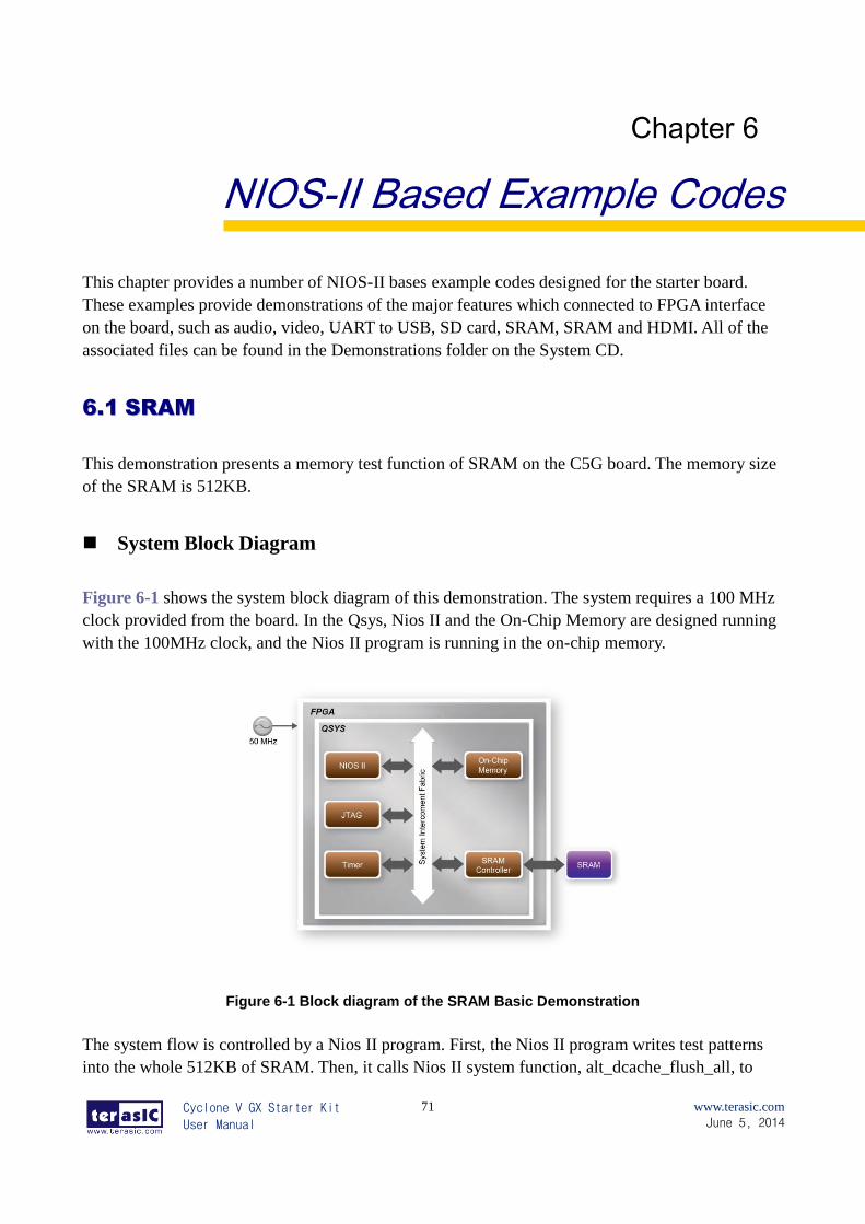
Cyclone V GX Starter Kit
User Manual
71
www.terasic.com
June 5, 2014
Chapter 6
NIOS-II Based Example Codes
This chapter provides a number of NIOS-II bases example codes designed for the starter board.
These examples provide demonstrations of the major features which connected to FPGA interface
on the board, such as audio, video, UART to USB, SD card, SRAM, SRAM and HDMI. All of the
associated files can be found in the Demonstrations folder on the System CD.
66..11 SSRRAAMM
This demonstration presents a memory test function of SRAM on the C5G board. The memory size
of the SRAM is 512KB.
System Block Diagram
Figure 6-1 shows the system block diagram of this demonstration. The system requires a 100 MHz
clock provided from the board. In the Qsys, Nios II and the On-Chip Memory are designed running
with the 100MHz clock, and the Nios II program is running in the on-chip memory.
Figure 6-1 Block diagram of the SRAM Basic Demonstration
The system flow is controlled by a Nios II program. First, the Nios II program writes test patterns
into the whole 512KB of SRAM. Then, it calls Nios II system function, alt_dcache_flush_all, to
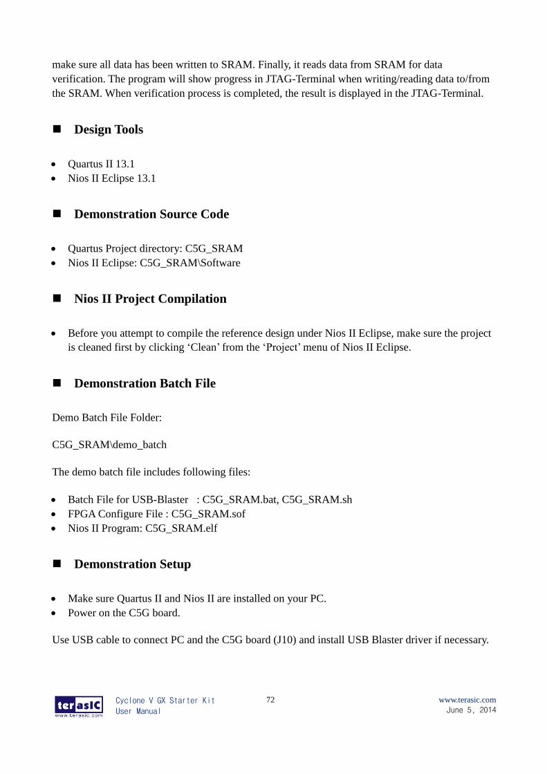
Cyclone V GX Starter Kit
User Manual
72
www.terasic.com
June 5, 2014
make sure all data has been written to SRAM. Finally, it reads data from SRAM for data
verification. The program will show progress in JTAG-Terminal when writing/reading data to/from
the SRAM. When verification process is completed, the result is displayed in the JTAG-Terminal.
Design Tools
Quartus II 13.1
Nios II Eclipse 13.1
Demonstration Source Code
Quartus Project directory: C5G_SRAM
Nios II Eclipse: C5G_SRAM\Software
Nios II Project Compilation
Before you attempt to compile the reference design under Nios II Eclipse, make sure the project
is cleaned first by clicking ‘Clean’ from the ‘Project’ menu of Nios II Eclipse.
Demonstration Batch File
Demo Batch File Folder:
C5G_SRAM\demo_batch
The demo batch file includes following files:
Batch File for USB-Blaster : C5G_SRAM.bat, C5G_SRAM.sh
FPGA Configure File : C5G_SRAM.sof
Nios II Program: C5G_SRAM.elf
Demonstration Setup
Make sure Quartus II and Nios II are installed on your PC.
Power on the C5G board.
Use USB cable to connect PC and the C5G board (J10) and install USB Blaster driver if necessary.
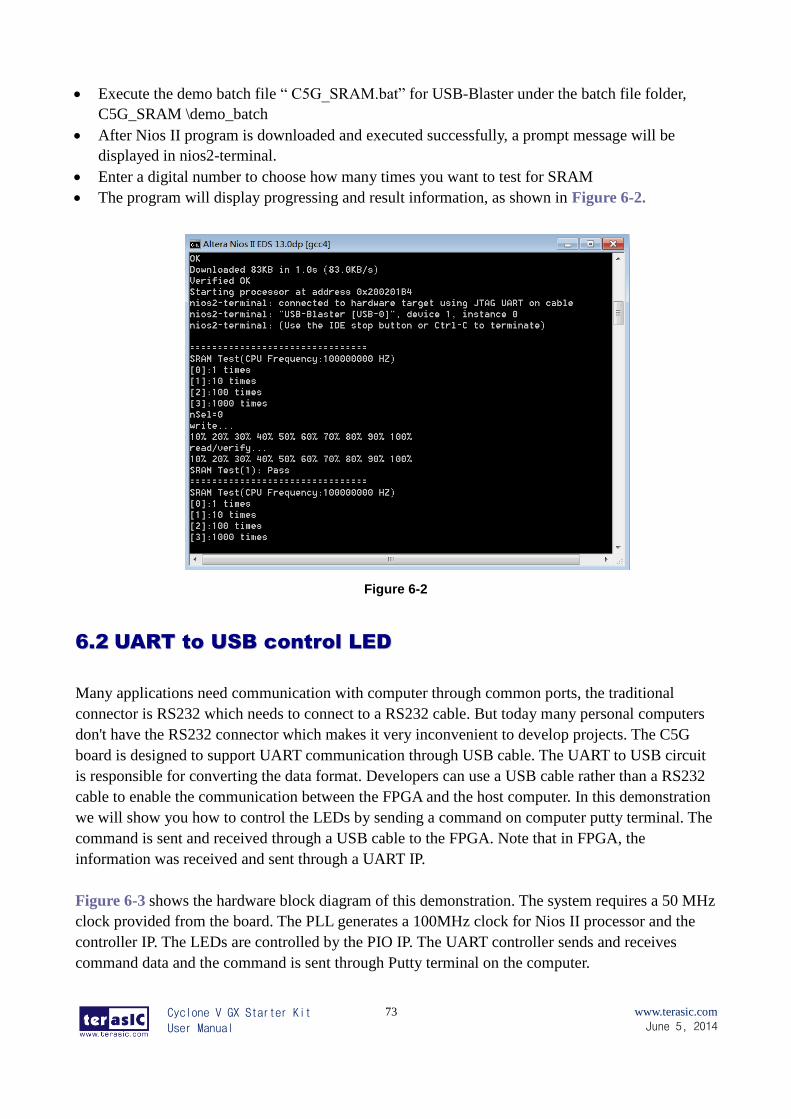
Cyclone V GX Starter Kit
User Manual
73
www.terasic.com
June 5, 2014
Execute the demo batch file “ C5G_SRAM.bat” for USB-Blaster under the batch file folder,
C5G_SRAM \demo_batch
After Nios II program is downloaded and executed successfully, a prompt message will be
displayed in nios2-terminal.
Enter a digital number to choose how many times you want to test for SRAM
The program will display progressing and result information, as shown in Figure 6-2.
Figure 6-2
66..22 UUAARRTT ttoo UUSSBB ccoonnttrrooll LLEEDD
Many applications need communication with computer through common ports, the traditional
connector is RS232 which needs to connect to a RS232 cable. But today many personal computers
don't have the RS232 connector which makes it very inconvenient to develop projects. The C5G
board is designed to support UART communication through USB cable. The UART to USB circuit
is responsible for converting the data format. Developers can use a USB cable rather than a RS232
cable to enable the communication between the FPGA and the host computer. In this demonstration
we will show you how to control the LEDs by sending a command on computer putty terminal. The
command is sent and received through a USB cable to the FPGA. Note that in FPGA, the
information was received and sent through a UART IP.
Figure 6-3 shows the hardware block diagram of this demonstration. The system requires a 50 MHz
clock provided from the board. The PLL generates a 100MHz clock for Nios II processor and the
controller IP. The LEDs are controlled by the PIO IP. The UART controller sends and receives
command data and the command is sent through Putty terminal on the computer.
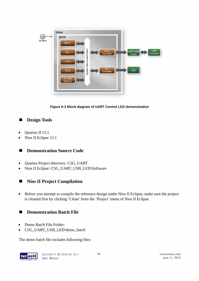
Cyclone V GX Starter Kit
User Manual
74
www.terasic.com
June 5, 2014
Figure 6-3 Block diagram of UART Control LED demonstration
Design Tools
Quartus II 13.1
Nios II Eclipse 13.1
Demonstration Source Code
Quartus Project directory: C5G_UART
Nios II Eclipse: C5G_UART_USB_LED\Software
Nios II Project Compilation
Before you attempt to compile the reference design under Nios II Eclipse, make sure the project
is cleaned first by clicking ‘Clean’ from the ‘Project’ menu of Nios II Eclipse.
Demonstration Batch File
Demo Batch File Folder:
C5G_UART_USB_LED\demo_batch
The demo batch file includes following files:
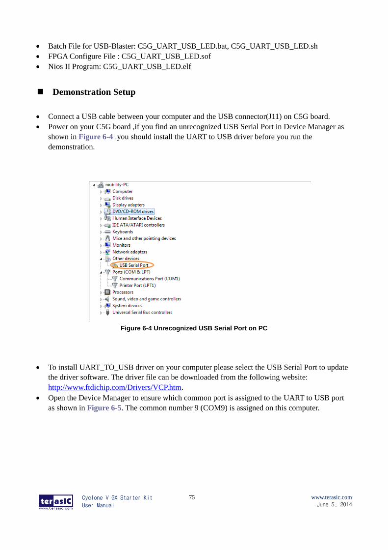
Cyclone V GX Starter Kit
User Manual
75
www.terasic.com
June 5, 2014
Batch File for USB-Blaster: C5G_UART_USB_LED.bat, C5G_UART_USB_LED.sh
FPGA Configure File : C5G_UART_USB_LED.sof
Nios II Program: C5G_UART_USB_LED.elf
Demonstration Setup
Connect a USB cable between your computer and the USB connector(J11) on C5G board.
Power on your C5G board ,if you find an unrecognized USB Serial Port in Device Manager as
shown in Figure 6-4 .you should install the UART to USB driver before you run the
demonstration.
Figure 6-4 Unrecognized USB Serial Port on PC
To install UART_TO_USB driver on your computer please select the USB Serial Port to update
the driver software. The driver file can be downloaded from the following website:
http://www.ftdichip.com/Drivers/VCP.htm.
Open the Device Manager to ensure which common port is assigned to the UART to USB port
as shown in Figure 6-5. The common number 9 (COM9) is assigned on this computer.
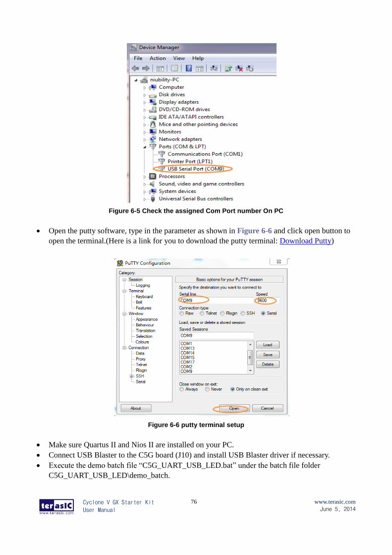
Cyclone V GX Starter Kit
User Manual
76
www.terasic.com
June 5, 2014
Figure 6-5 Check the assigned Com Port number On PC
Open the putty software, type in the parameter as shown in Figure 6-6 and click open button to
open the terminal.(Here is a link for you to download the putty terminal: Download Putty)
Figure 6-6 putty terminal setup
Make sure Quartus II and Nios II are installed on your PC.
Connect USB Blaster to the C5G board (J10) and install USB Blaster driver if necessary.
Execute the demo batch file “C5G_UART_USB_LED.bat” under the batch file folder
C5G_UART_USB_LED\demo_batch.
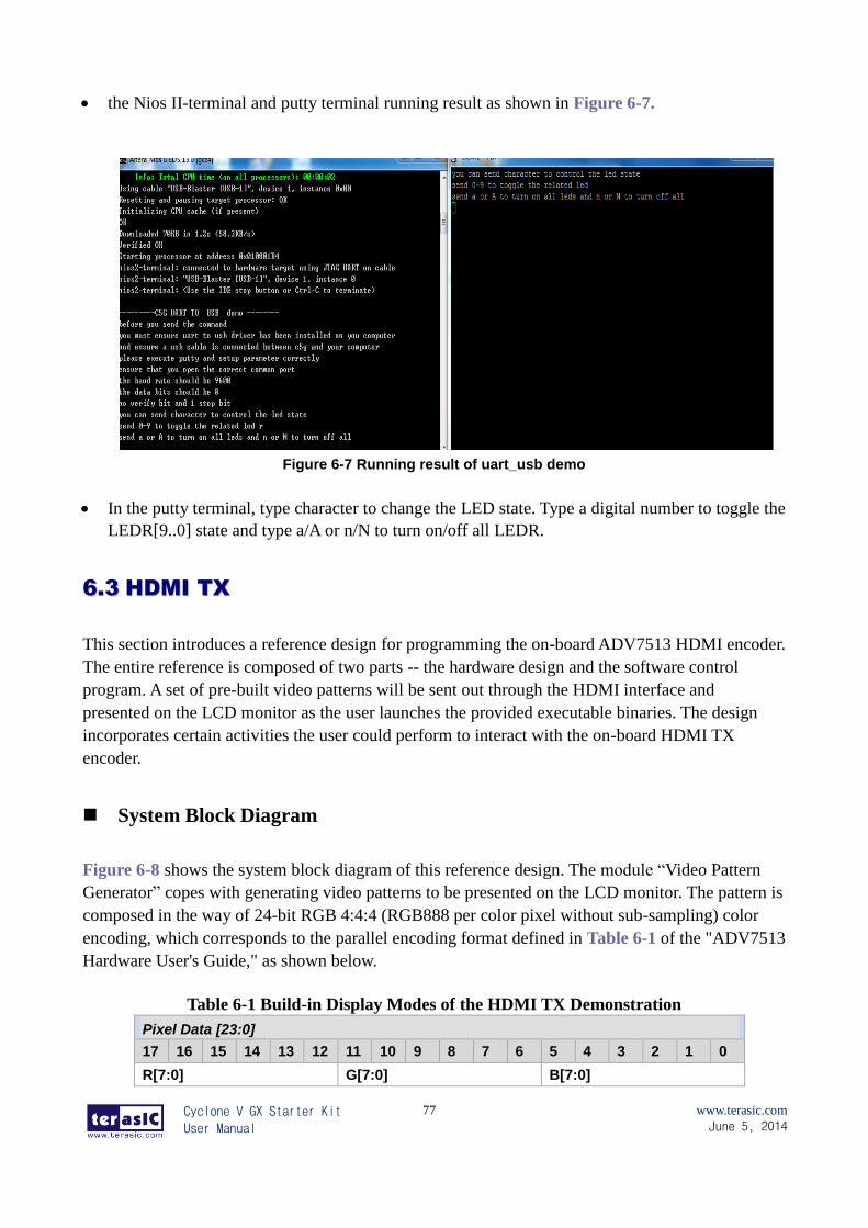
Cyclone V GX Starter Kit
User Manual
77
www.terasic.com
June 5, 2014
the Nios II-terminal and putty terminal running result as shown in Figure 6-7.
Figure 6-7 Running result of uart_usb demo
In the putty terminal, type character to change the LED state. Type a digital number to toggle the
LEDR[9..0] state and type a/A or n/N to turn on/off all LEDR.
66..33 HHDDMMII TTXX
This section introduces a reference design for programming the on-board ADV7513 HDMI encoder.
The entire reference is composed of two parts -- the hardware design and the software control
program. A set of pre-built video patterns will be sent out through the HDMI interface and
presented on the LCD monitor as the user launches the provided executable binaries. The design
incorporates certain activities the user could perform to interact with the on-board HDMI TX
encoder.
System Block Diagram
Figure 6-8 shows the system block diagram of this reference design. The module “Video Pattern
Generator” copes with generating video patterns to be presented on the LCD monitor. The pattern is
composed in the way of 24-bit RGB 4:4:4 (RGB888 per color pixel without sub-sampling) color
encoding, which corresponds to the parallel encoding format defined in Table 6-1 of the "ADV7513
Hardware User's Guide," as shown below.
Table 6-1 Build-in Display Modes of the HDMI TX Demonstration
Pixel Data [23:0]
17 16 15 14 13 12 11 10 9 8 7 6 5 4 3 2 1 0
R[7:0] G[7:0] B[7:0]
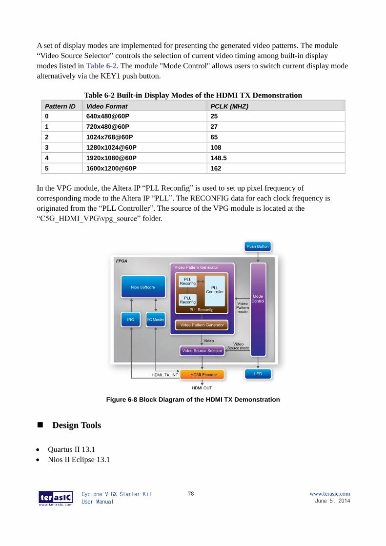
Cyclone V GX Starter Kit
User Manual
78
www.terasic.com
June 5, 2014
A set of display modes are implemented for presenting the generated video patterns. The module
“Video Source Selector” controls the selection of current video timing among built-in display
modes listed in Table 6-2. The module "Mode Control" allows users to switch current display mode
alternatively via the KEY1 push button.
Table 6-2 Built-in Display Modes of the HDMI TX Demonstration
Pattern ID Video Format PCLK (MHZ)
0 640x480@60P 25
1 720x480@60P 27
2 1024x768@60P 65
3 1280x1024@60P 108
4 1920x1080@60P 148.5
5 1600x1200@60P 162
In the VPG module, the Altera IP “PLL Reconfig” is used to set up pixel frequency of
corresponding mode to the Altera IP “PLL”. The RECONFIG data for each clock frequency is
originated from the “PLL Controller”. The source of the VPG module is located at the
“C5G_HDMI_VPG\vpg_source” folder.
Figure 6-8 Block Diagram of the HDMI TX Demonstration
Design Tools
Quartus II 13.1
Nios II Eclipse 13.1
Cyclone V GX Starter Kit
User Manual
79
www.terasic.com
June 5, 2014
Demonstration Source Code
Quartus Project directory: C5G_HDMI_VPG
Nios II Eclipse: C5G_HDMI_VPG\Software
Rebuild the Quartus II Project
Launch the " Quartus II 13.1" program and open the project file through the drop-down menu
"File" -> "Open." The pre-built Quartus II project file is named as "C5G_HDMI_VPG.qpf" in
the " C5G_HDMI_VPG " folder.
Users could follow the listed approaches below to rebuild a local copy of the FPGA SRAM (.sof)
file:
Launch the Qsys editor to inspect or modify the existing design. When asked for the location
of .qsys file, select the file name as "C5G_QSYS.qsys" in the "C5G_HDMI_VPG " folder.
If any changes were made to the design, press "Ctrl-S" to save the .qsys file and then click the
"Generation" tab to activate the "Generation" property page. Hit the "Generate" button below
the page to regenerate the SOPC file named as "HDMI_QSYS.sopcinfo" which would be used
to update the Nios II BSP project mentioned in the next section.
Switch back to the Quartus II program. Select "Processing" -> "Start Compilation" from the
drop-down menu or hit "Ctrl-L" to recompile the FPGA configuration file.
The newly built configuration file will be named as "C5G_HDMI_VPG.sof " in the
"C5G_HDMI_VPG " folder. You can copy it and overwrite the same binary in the
"demo_batch". Please refer to the "Launching the Demonstration" section for how to launch and
execute the demo.
Rebuild the Nios II Project
Launch the "Nios II 13.1 Software Build Tools for Eclipse" program. When the program asks
for the place of workspace, enter your local full path of the "C5G_HDMI_VPG\Software "
folder to the dialog's edit box.
Users could follow the approaches listed below to rebuild a local copy of the Nios II program:
Right-click on the HDMI_DEMO_bsp project in the Project Explore. Select "Nios II" ->
"Generate BSP."
Right-click on the HDMI_DEMO_bsp project in the Project Explore. Select "Clean Project."
Right-click on the HDMI_DEMO_bsp project in the Project Explore. Select "Build Project."
Right-click on the HDMI_DEMO project in the Project Explore. Select "Clean Project."
Right-click on the HDMI_DEMO project in the Project Explore. Select "Build Project."
The newly built binary will be located in the "C5G_HDMI_VPG\Software\HDMI_DEMO "
folder and named as "HDMI_DEMO.elf". You can copy it and overwrite the same binary in the
"demo_batch". Please refer to the "Launching the Demonstration" section for how to launch and
execute the demo.
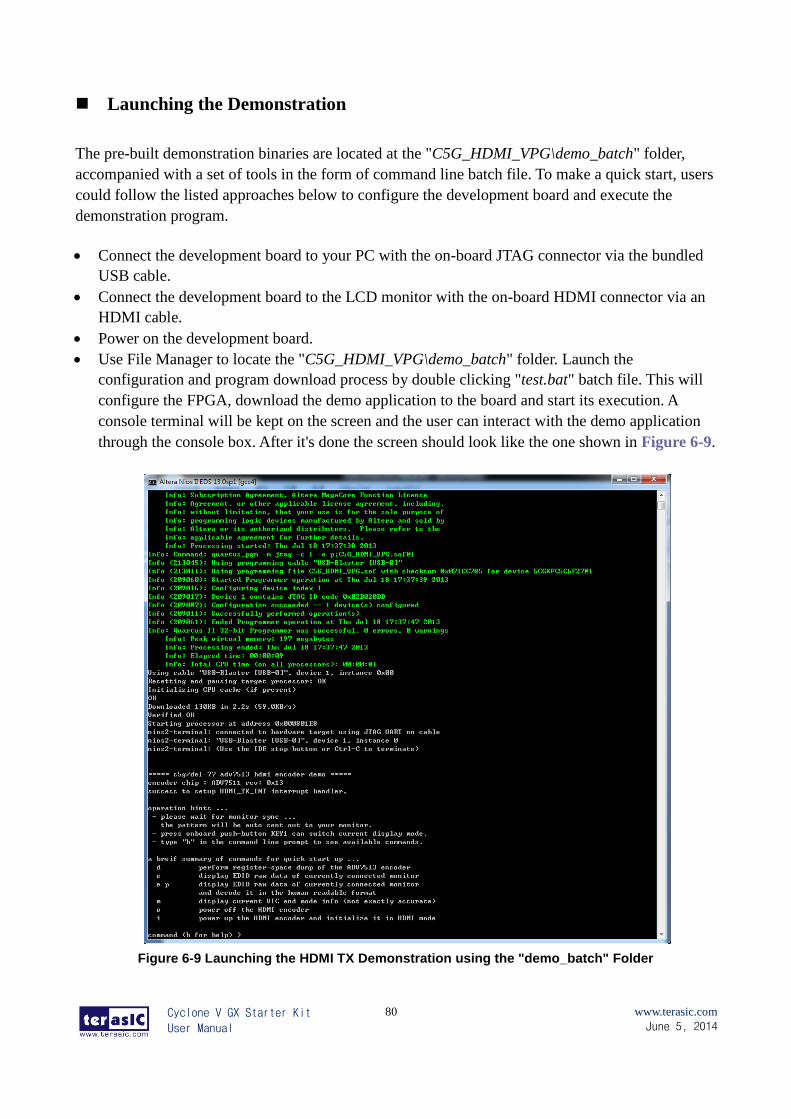
Cyclone V GX Starter Kit
User Manual
80
www.terasic.com
June 5, 2014
Launching the Demonstration
The pre-built demonstration binaries are located at the "C5G_HDMI_VPG\demo_batch" folder,
accompanied with a set of tools in the form of command line batch file. To make a quick start, users
could follow the listed approaches below to configure the development board and execute the
demonstration program.
Connect the development board to your PC with the on-board JTAG connector via the bundled
USB cable.
Connect the development board to the LCD monitor with the on-board HDMI connector via an
HDMI cable.
Power on the development board.
Use File Manager to locate the "C5G_HDMI_VPG\demo_batch" folder. Launch the
configuration and program download process by double clicking "test.bat" batch file. This will
configure the FPGA, download the demo application to the board and start its execution. A
console terminal will be kept on the screen and the user can interact with the demo application
through the console box. After it's done the screen should look like the one shown in Figure 6-9.
Figure 6-9 Launching the HDMI TX Demonstration using the "demo_batch" Folder
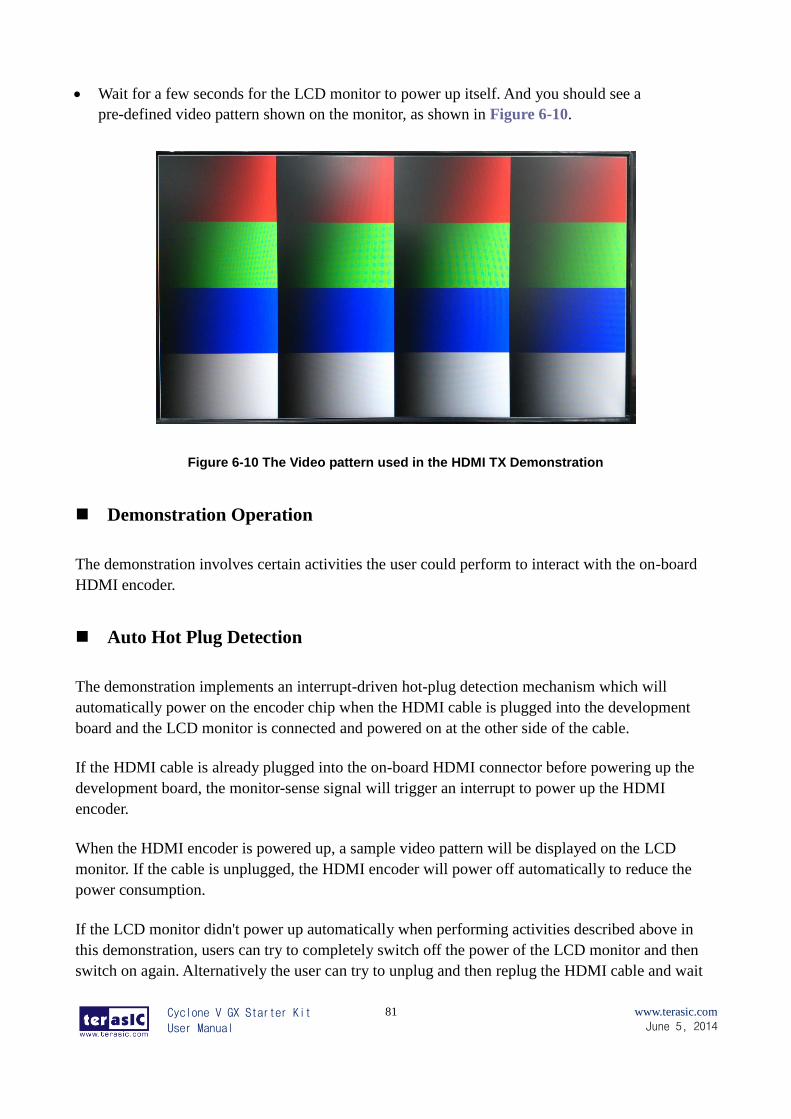
Cyclone V GX Starter Kit
User Manual
81
www.terasic.com
June 5, 2014
Wait for a few seconds for the LCD monitor to power up itself. And you should see a
pre-defined video pattern shown on the monitor, as shown in Figure 6-10.
Figure 6-10 The Video pattern used in the HDMI TX Demonstration
Demonstration Operation
The demonstration involves certain activities the user could perform to interact with the on-board
HDMI encoder.
Auto Hot Plug Detection
The demonstration implements an interrupt-driven hot-plug detection mechanism which will
automatically power on the encoder chip when the HDMI cable is plugged into the development
board and the LCD monitor is connected and powered on at the other side of the cable.
If the HDMI cable is already plugged into the on-board HDMI connector before powering up the
development board, the monitor-sense signal will trigger an interrupt to power up the HDMI
encoder.
When the HDMI encoder is powered up, a sample video pattern will be displayed on the LCD
monitor. If the cable is unplugged, the HDMI encoder will power off automatically to reduce the
power consumption.
If the LCD monitor didn't power up automatically when performing activities described above in
this demonstration, users can try to completely switch off the power of the LCD monitor and then
switch on again. Alternatively the user can try to unplug and then replug the HDMI cable and wait
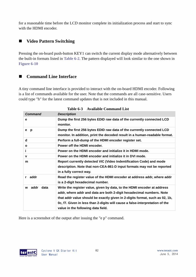
Cyclone V GX Starter Kit
User Manual
82
www.terasic.com
June 5, 2014
for a reasonable time before the LCD monitor complete its initialization process and start to sync
with the HDMI encoder.
Video Pattern Switching
Pressing the on-board push-button KEY1 can switch the current display mode alternatively between
the built-in formats listed in Table 6-2. The pattern displayed will look similar to the one shown in
Figure 6-10
Command Line Interface
A tiny command line interface is provided to interact with the on-board HDMI encoder. Following
is a list of commands available for the user. Note that the commands are all case-sensitive. Users
could type "h" for the latest command updates that is not included in this manual.
Table 6-3 Available Command List
Command Description
e Dump the first 256 bytes EDID raw data of the currently connected LCD
monitor.
e p Dump the first 256 bytes EDID raw data of the currently connected LCD
monitor. In addition, print the decoded result in a human-readable format.
d Perform a full-dump of the HDMI encoder register set.
o Power off the HDMI encoder.
i Power on the HDMI encoder and initialize it in HDMI mode.
v Power on the HDMI encoder and initialize it in DVI mode.
m Report currently detected VIC (Video Indentification Code) and mode
description. Note that non-CEA-861-D input formats may not be reported
in a fully correct way.
r addr Read the register value of the HDMI encoder at address addr, where addr
is a 2-digit hexadecimal number.
w addr data Write the register value, given by data, to the HDMI encoder at address
addr, where addr and data are both 2-digit hexadecimal numbers. Note
that addr value should be exactly given in 2-digits format, such as 02, 1b,
0c, f7. Given in less than 2-digits will cause a false-interpretation of the
value in the following data field.
Here is a screenshot of the output after issuing the "e p" command.
Cyclone V GX Starter Kit
User Manual
83
www.terasic.com
June 5, 2014
Figure 6-11 The EDID Decoder Output of the HDMI TX Demonstration
66..44 TTrraannsscceeiivveerr HHSSMMCC LLooooppbbaacckk tteesstt
The XCVR HSMC loopback demonstration is a project to test XCVR HSMC Loopback function.
The system generates data pattern and transports data through the XCVR channel. Meanwhile, the
system receives the data through the loopback daughter card and checks it. Altera IP data pattern
generator and data pattern checker are responsible for generating and checking the data pattern. The
Nios II CPU checks the test result. The test result is shown through LEDG0~LEDG3 and also
displayed in the Nios-II terminal. If the loopback test function is not working, the program will
terminate and the all LEDs will be turned off.
Design Tools
Quartus II 13.1
Nios II Eclipse 13.1
Demonstration Source Code
Quartus Project directory: C5G_HSMC_XCVR_LOOPBACK_TEST
Nios II Eclipse: C5G_HSMC_XCVR_LOOPBACK_TEST\Software
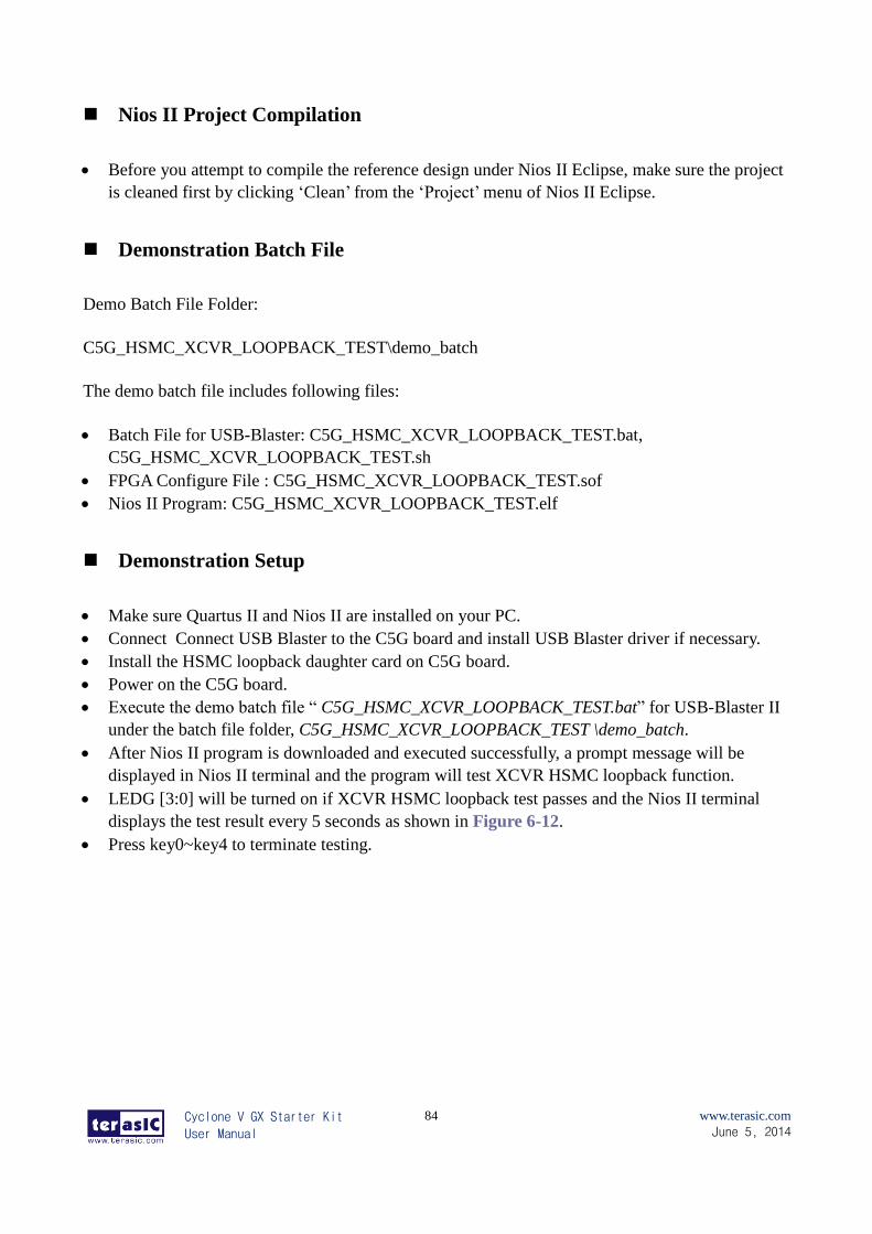
Cyclone V GX Starter Kit
User Manual
84
www.terasic.com
June 5, 2014
Nios II Project Compilation
Before you attempt to compile the reference design under Nios II Eclipse, make sure the project
is cleaned first by clicking ‘Clean’ from the ‘Project’ menu of Nios II Eclipse.
Demonstration Batch File
Demo Batch File Folder:
C5G_HSMC_XCVR_LOOPBACK_TEST\demo_batch
The demo batch file includes following files:
Batch File for USB-Blaster: C5G_HSMC_XCVR_LOOPBACK_TEST.bat,
C5G_HSMC_XCVR_LOOPBACK_TEST.sh
FPGA Configure File : C5G_HSMC_XCVR_LOOPBACK_TEST.sof
Nios II Program: C5G_HSMC_XCVR_LOOPBACK_TEST.elf
Demonstration Setup
Make sure Quartus II and Nios II are installed on your PC.
Connect Connect USB Blaster to the C5G board and install USB Blaster driver if necessary.
Install the HSMC loopback daughter card on C5G board.
Power on the C5G board.
Execute the demo batch file “ C5G_HSMC_XCVR_LOOPBACK_TEST.bat” for USB-Blaster II
under the batch file folder, C5G_HSMC_XCVR_LOOPBACK_TEST \demo_batch.
After Nios II program is downloaded and executed successfully, a prompt message will be
displayed in Nios II terminal and the program will test XCVR HSMC loopback function.
LEDG [3:0] will be turned on if XCVR HSMC loopback test passes and the Nios II terminal
displays the test result every 5 seconds as shown in Figure 6-12.
Press key0~key4 to terminate testing.
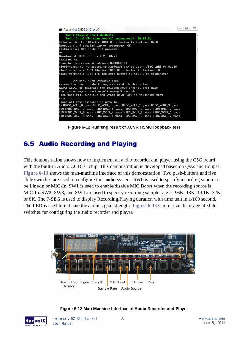
Cyclone V GX Starter Kit
User Manual
85
www.terasic.com
June 5, 2014
Figure 6-12 Running result of XCVR HSMC loopback test
66..55 AAuuddiioo RReeccoorrddiinngg aanndd PPllaayyiinngg
This demonstration shows how to implement an audio recorder and player using the C5G board
with the built-in Audio CODEC chip. This demonstration is developed based on Qsys and Eclipse.
Figure 6-13 shows the man-machine interface of this demonstration. Two push-buttons and five
slide switches are used to configure this audio system: SW0 is used to specify recording source to
be Line-in or MIC-In. SW1 is used to enable/disable MIC Boost when the recording source is
MIC-In. SW2, SW3, and SW4 are used to specify recording sample rate as 96K, 48K, 44.1K, 32K,
or 8K. The 7-SEG is used to display Recording/Playing duration with time unit in 1/100 second.
The LED is used to indicate the audio signal strength. Figure 6-13 summarize the usage of slide
switches for configuring the audio recorder and player.
Figure 6-13 Man-Machine Interface of Audio Recorder and Player
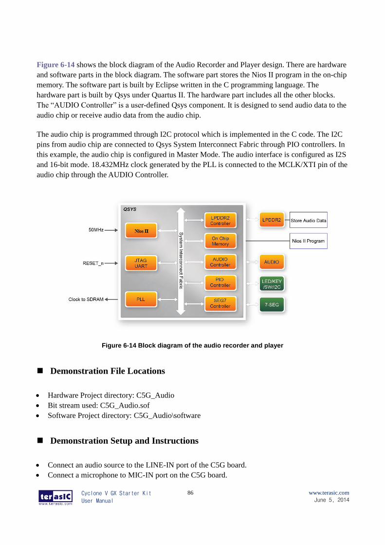
Cyclone V GX Starter Kit
User Manual
86
www.terasic.com
June 5, 2014
Figure 6-14 shows the block diagram of the Audio Recorder and Player design. There are hardware
and software parts in the block diagram. The software part stores the Nios II program in the on-chip
memory. The software part is built by Eclipse written in the C programming language. The
hardware part is built by Qsys under Quartus II. The hardware part includes all the other blocks.
The “AUDIO Controller” is a user-defined Qsys component. It is designed to send audio data to the
audio chip or receive audio data from the audio chip.
The audio chip is programmed through I2C protocol which is implemented in the C code. The I2C
pins from audio chip are connected to Qsys System Interconnect Fabric through PIO controllers. In
this example, the audio chip is configured in Master Mode. The audio interface is configured as I2S
and 16-bit mode. 18.432MHz clock generated by the PLL is connected to the MCLK/XTI pin of the
audio chip through the AUDIO Controller.
Figure 6-14 Block diagram of the audio recorder and player
Demonstration File Locations
Hardware Project directory: C5G_Audio
Bit stream used: C5G_Audio.sof
Software Project directory: C5G_Audio\software
Demonstration Setup and Instructions
Connect an audio source to the LINE-IN port of the C5G board.
Connect a microphone to MIC-IN port on the C5G board.
Cyclone V GX Starter Kit
User Manual
87
www.terasic.com
June 5, 2014
Connect a speaker or headset to LINE-OUT port on the C5G board.
Load the bit stream into FPGA. (note *1)
Load the software execution file into FPGA. (note *1)
Configure audio with the slide switches as shown in Table 6-4.
Press KEY3 on the C5G board to start/stop audio recording (note *2)
Press KEY2 on the C5G board to start/stop audio playing (note *3)
Table 6-4 Slide switches usage for audio source
Slide Switches 0 – DOWN Position 1 – UP Position
SW0 Audio is from MIC Audio is from LINE-IN
SW1 Disable MIC Boost Enable MIC Boost
Table 6-5 Slide switch setting for sample rate switching for audio recorder and player
SW4
(0 – DOWN;
1- UP)
SW3
(0 – DOWN;
1-UP)
SW2
(0 – DOWN;
1-UP)
Sample Rate
0 0 0 96K
0 0 1 48K
0 1 0 44.1K
0 1 1 32K
1 0 0 8K
Unlisted combination 96K
Note:
(1) Execute C5G_Audio \demo_batch\ C5G_Audio.bat will download .sof and .elf files.
(2) Recording process will stop if audio buffer is full.
(3) Playing process will stop if audio data is played completely.
66..66 MMiiccrroo SSDD CCaarrdd ffiillee ssyysstteemm rreeaadd
Many applications use a large external storage device, such as a SD Card or CF card to store data.
The C5G board provides the hardware and software needed for Micro SD Card access. In this
demonstration we will show how to browse files stored in the root directory of an SD Card and how
to read the file contents of a specific file. The Micro SD Card is required to be formatted as FAT
File System in advance. Long file name is supported in this demonstration. Figure 6-15 shows the
hardware system block diagram of this demonstration. The system requires a 50MHz clock
provided by the board. The PLL generates a 100MHz clock for the Nios II processor and other
controllers. Four PIO pins are connected to the Micro SD Card socket. SD 4-bit Mode is used to
access the Micro SD Card hardware. The SD 4-bit protocol and FAT File System function are all
implemented by Nios II software. The software is stored in the on-chip memory.
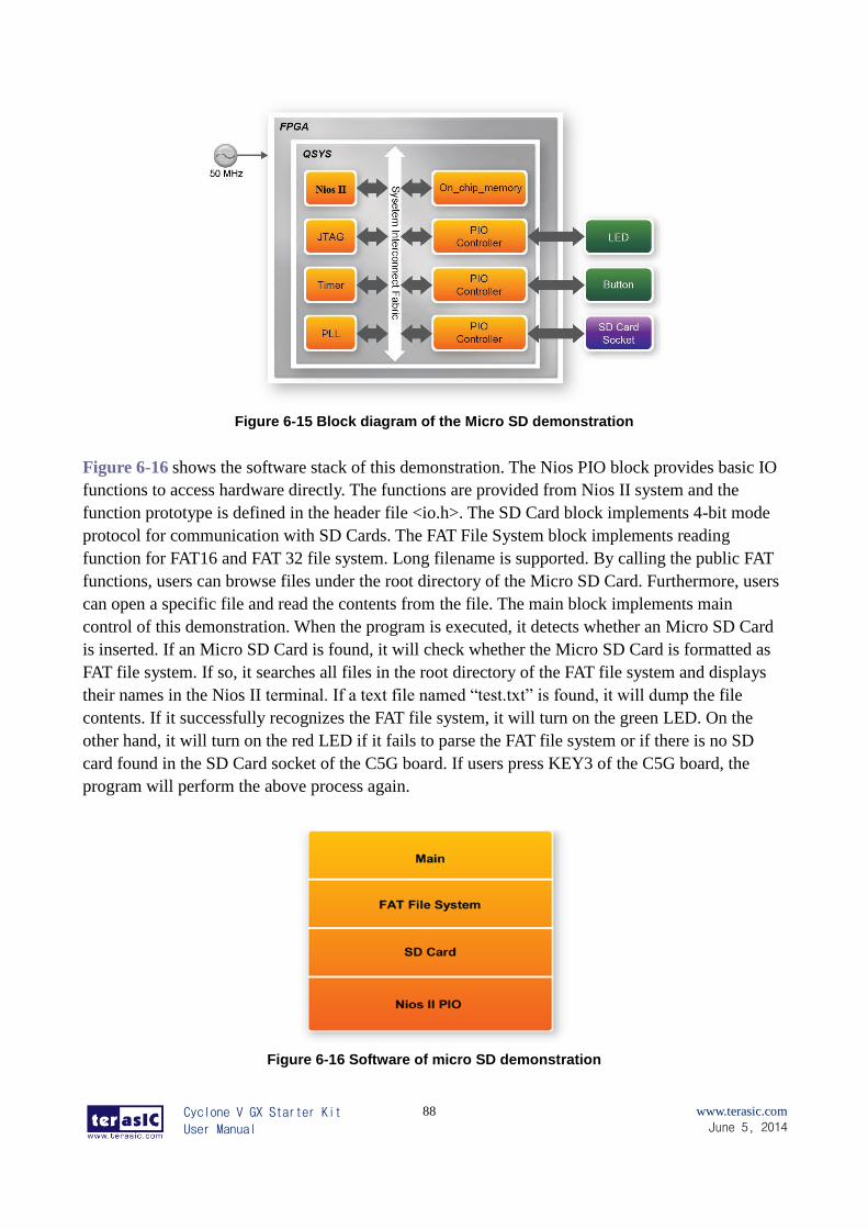
Cyclone V GX Starter Kit
User Manual
88
www.terasic.com
June 5, 2014
Figure 6-15 Block diagram of the Micro SD demonstration
Figure 6-16 shows the software stack of this demonstration. The Nios PIO block provides basic IO
functions to access hardware directly. The functions are provided from Nios II system and the
function prototype is defined in the header file <io.h>. The SD Card block implements 4-bit mode
protocol for communication with SD Cards. The FAT File System block implements reading
function for FAT16 and FAT 32 file system. Long filename is supported. By calling the public FAT
functions, users can browse files under the root directory of the Micro SD Card. Furthermore, users
can open a specific file and read the contents from the file. The main block implements main
control of this demonstration. When the program is executed, it detects whether an Micro SD Card
is inserted. If an Micro SD Card is found, it will check whether the Micro SD Card is formatted as
FAT file system. If so, it searches all files in the root directory of the FAT file system and displays
their names in the Nios II terminal. If a text file named “test.txt” is found, it will dump the file
contents. If it successfully recognizes the FAT file system, it will turn on the green LED. On the
other hand, it will turn on the red LED if it fails to parse the FAT file system or if there is no SD
card found in the SD Card socket of the C5G board. If users press KEY3 of the C5G board, the
program will perform the above process again.
Figure 6-16 Software of micro SD demonstration
Cyclone V GX Starter Kit
User Manual
89
www.terasic.com
June 5, 2014
Design Tools
Quartus II 13.1
Nios II Eclipse 13.1
Demonstration Source Code
Quartus Project directory: C5G_SD_DEMO
Nios II Eclipse: C5G_SD_DEMO\Software
Nios II Project Compilation
Before you attempt to compile the reference design under Nios II Eclipse, make sure the project
is cleaned first by clicking ‘Clean’ from the ‘Project’ menu of Nios II Eclipse.
Demonstration Batch File
Demo Batch File Folder:
C5G_SD_DEMO \demo_batch
The demo batch file includes following files:
Batch File for USB-Blaster :
C5G_SD_DEMO.bat,
C5G_SD_DEMO.sh
FPGA Configure File : C5G_SD_DEMO.sof
Nios II Program:C5G_SD_DEMO.elf
Demonstration Setup
Make sure Quartus II and Nios II are installed on your PC.
Power on the C5G board.
Connect USB Blaster to the C5G board and install USB Blaster driver if necessary.
Execute the demo batch file “C5G_SD_DEMO.bat” for USB-Blaster II under the batch file
folder, C5G_SD_DEMO\demo_batch
After Nios II program is downloaded and executed successfully, a prompt message will be
displayed in nios2-terminal.
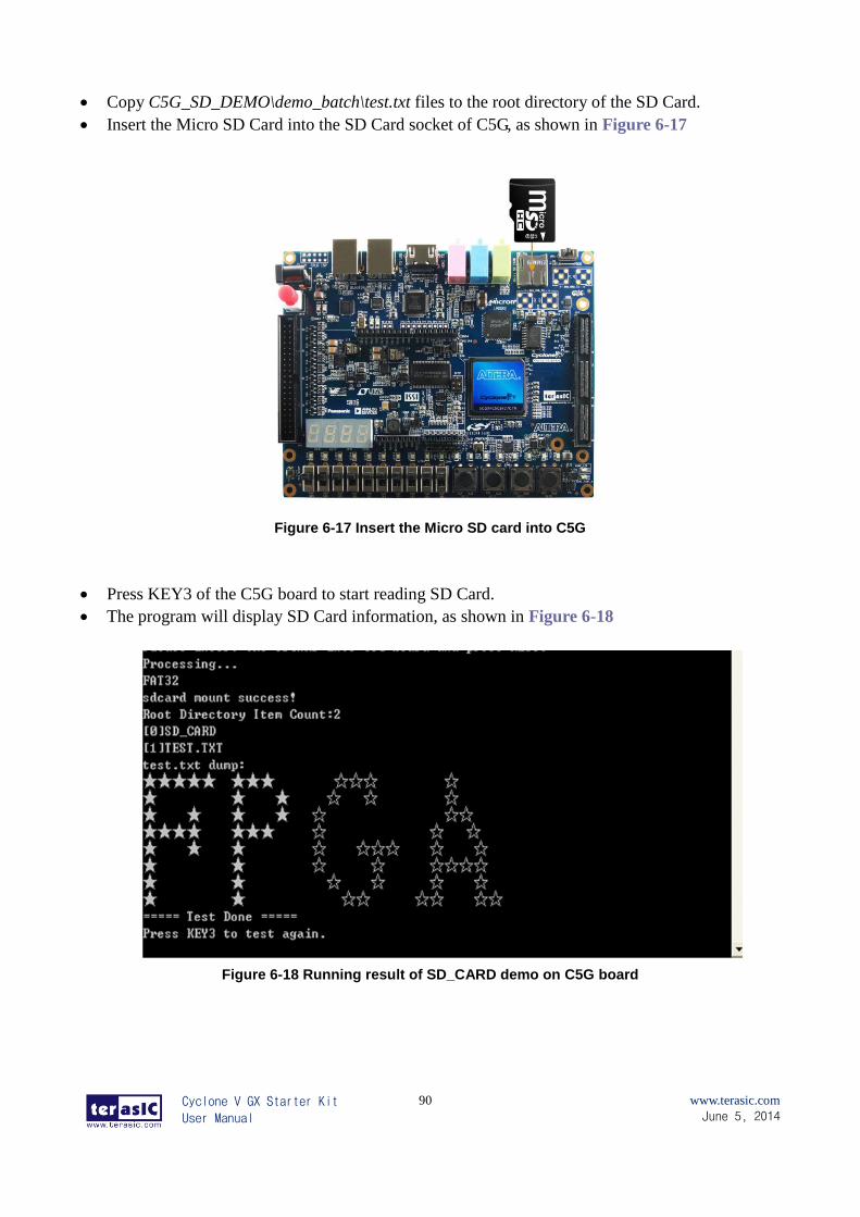
Cyclone V GX Starter Kit
User Manual
90
www.terasic.com
June 5, 2014
Copy C5G_SD_DEMO\demo_batch\test.txt files to the root directory of the SD Card.
Insert the Micro SD Card into the SD Card socket of C5G, as shown in Figure 6-17
Figure 6-17 Insert the Micro SD card into C5G
Press KEY3 of the C5G board to start reading SD Card.
The program will display SD Card information, as shown in Figure 6-18
Figure 6-18 Running result of SD_CARD demo on C5G board
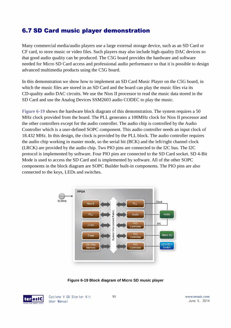
Cyclone V GX Starter Kit
User Manual
91
www.terasic.com
June 5, 2014
66..77 SSDD CCaarrdd mmuussiicc ppllaayyeerr ddeemmoonnssttrraattiioonn
Many commercial media/audio players use a large external storage device, such as an SD Card or
CF card, to store music or video files. Such players may also include high-quality DAC devices so
that good audio quality can be produced. The C5G board provides the hardware and software
needed for Micro SD Card access and professional audio performance so that it is possible to design
advanced multimedia products using the C5G board.
In this demonstration we show how to implement an SD Card Music Player on the C5G board, in
which the music files are stored in an SD Card and the board can play the music files via its
CD-quality audio DAC circuits. We use the Nios II processor to read the music data stored in the
SD Card and use the Analog Devices SSM2603 audio CODEC to play the music.
Figure 6-19 shows the hardware block diagram of this demonstration. The system requires a 50
MHz clock provided from the board. The PLL generates a 100MHz clock for Nios II processor and
the other controllers except for the audio controller. The audio chip is controlled by the Audio
Controller which is a user-defined SOPC component. This audio controller needs an input clock of
18.432 MHz. In this design, the clock is provided by the PLL block. The audio controller requires
the audio chip working in master mode, so the serial bit (BCK) and the left/right channel clock
(LRCK) are provided by the audio chip. Two PIO pins are connected to the I2C bus. The I2C
protocol is implemented by software. Four PIO pins are connected to the SD Card socket. SD 4-Bit
Mode is used to access the SD Card and is implemented by software. All of the other SOPC
components in the block diagram are SOPC Builder built-in components. The PIO pins are also
connected to the keys, LEDs and switches.
Figure 6-19 Block diagram of Micro SD music player
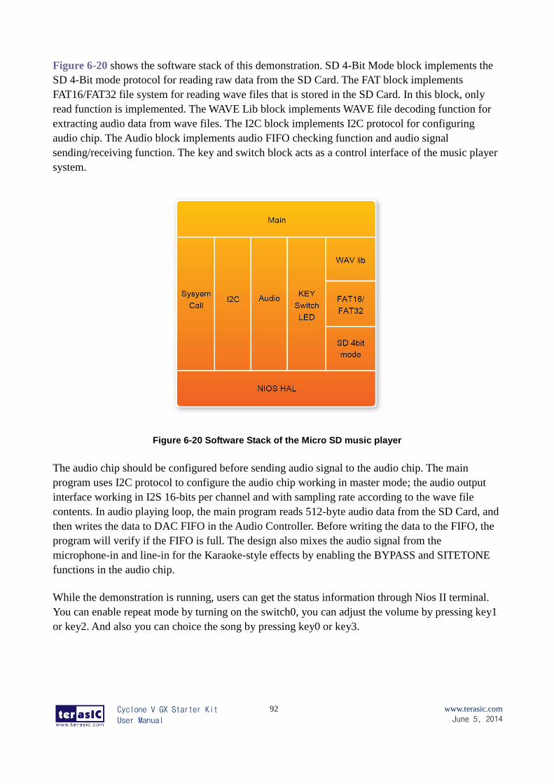
Cyclone V GX Starter Kit
User Manual
92
www.terasic.com
June 5, 2014
Figure 6-20 shows the software stack of this demonstration. SD 4-Bit Mode block implements the
SD 4-Bit mode protocol for reading raw data from the SD Card. The FAT block implements
FAT16/FAT32 file system for reading wave files that is stored in the SD Card. In this block, only
read function is implemented. The WAVE Lib block implements WAVE file decoding function for
extracting audio data from wave files. The I2C block implements I2C protocol for configuring
audio chip. The Audio block implements audio FIFO checking function and audio signal
sending/receiving function. The key and switch block acts as a control interface of the music player
system.
Figure 6-20 Software Stack of the Micro SD music player
The audio chip should be configured before sending audio signal to the audio chip. The main
program uses I2C protocol to configure the audio chip working in master mode; the audio output
interface working in I2S 16-bits per channel and with sampling rate according to the wave file
contents. In audio playing loop, the main program reads 512-byte audio data from the SD Card, and
then writes the data to DAC FIFO in the Audio Controller. Before writing the data to the FIFO, the
program will verify if the FIFO is full. The design also mixes the audio signal from the
microphone-in and line-in for the Karaoke-style effects by enabling the BYPASS and SITETONE
functions in the audio chip.
While the demonstration is running, users can get the status information through Nios II terminal.
You can enable repeat mode by turning on the switch0, you can adjust the volume by pressing key1
or key2. And also you can choice the song by pressing key0 or key3.
Cyclone V GX Starter Kit
User Manual
93
www.terasic.com
June 5, 2014
Design Tools
Quartus II 13.1
Nios II Eclipse 13.1
Demonstration Source Code
Quartus Project directory: C5G_SD_MUSIC
Nios II Eclipse: C5G_SD_MUSIC\Software
Nios II Project Compilation
Before you attempt to compile the reference design under Nios II Eclipse, make sure the project
is cleaned first by clicking ‘Clean’ from the ‘Project’ menu of Nios II Eclipse.
Demonstration Batch File
Demo Batch File Folder:
C5G_SD_MUSIC\demo_batch
The demo batch file includes following files:
Batch File for USB-Blaster : C5G_SD_MUSIC.bat, C5G_SD_MUSIC.sh
FPGA Configure File :C5G_SD_MUSIC.sof
Nios II Program: C5G_SD_MUSIC.elf
Demonstration Setup
Format your Micro SD Card into FAT16/FAT32 format
Place the wave files to the root directory of the Micro SD Card. The provided wave files must
have a sample rate of either 96K, 48K, 44.1K, 32K, or 8K. In addition, the wave files must be
stereo and 16 bits per channel.
Connect a headset or speaker to the C5G board and you should be able to hear the music played
from the Micro SD Card
Insert the Micro SD card into the SD socket on C5G board.
Make sure Quartus II and Nios II are installed on your PC.
Power on the C5G board.
Connect USB Blaster to the C5G board and install USB Blaster driver if necessary.
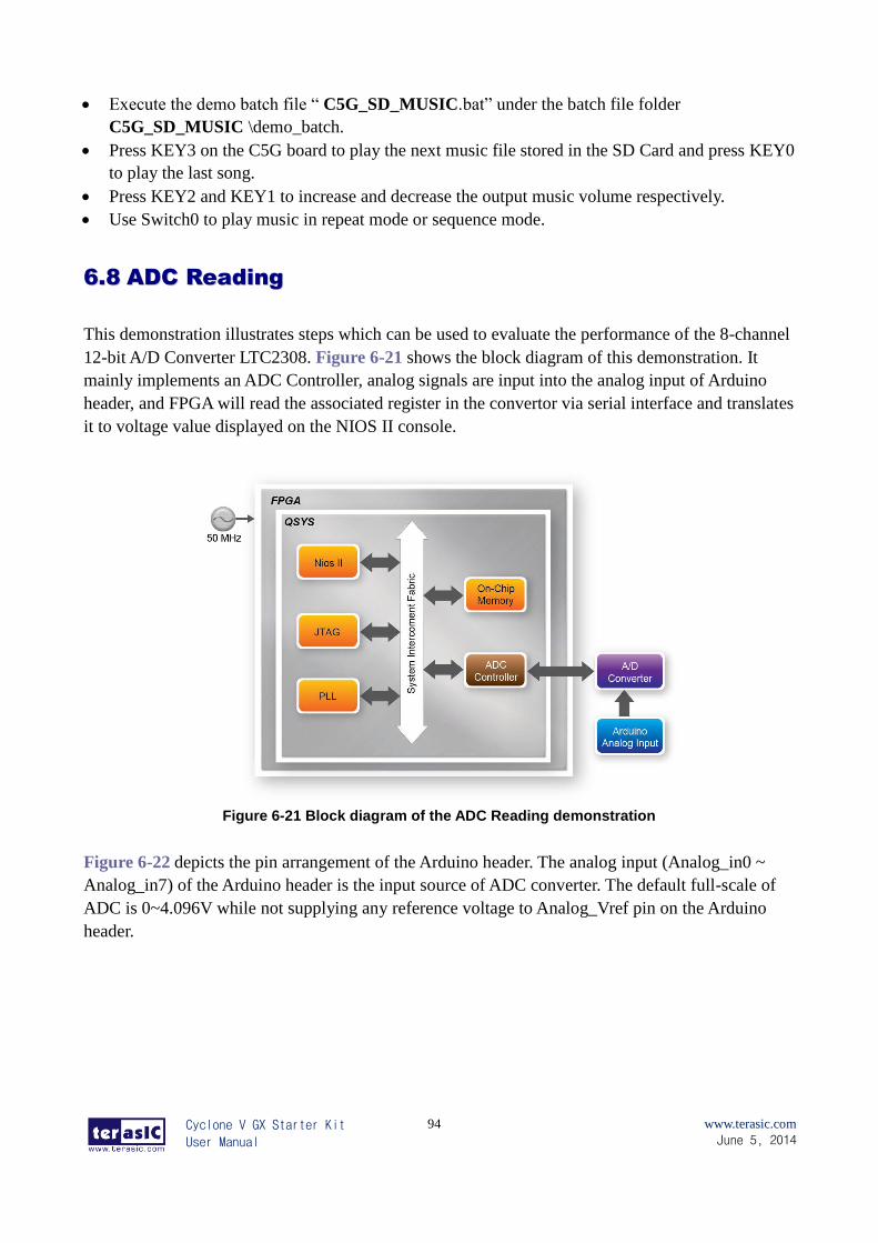
Cyclone V GX Starter Kit
User Manual
94
www.terasic.com
June 5, 2014
Execute the demo batch file “ C5G_SD_MUSIC.bat” under the batch file folder
C5G_SD_MUSIC \demo_batch.
Press KEY3 on the C5G board to play the next music file stored in the SD Card and press KEY0
to play the last song.
Press KEY2 and KEY1 to increase and decrease the output music volume respectively.
Use Switch0 to play music in repeat mode or sequence mode.
66..88 AADDCC RReeaaddiinngg
This demonstration illustrates steps which can be used to evaluate the performance of the 8-channel
12-bit A/D Converter LTC2308. Figure 6-21 shows the block diagram of this demonstration. It
mainly implements an ADC Controller, analog signals are input into the analog input of Arduino
header, and FPGA will read the associated register in the convertor via serial interface and translates
it to voltage value displayed on the NIOS II console.
Figure 6-21 Block diagram of the ADC Reading demonstration
Figure 6-22 depicts the pin arrangement of the Arduino header. The analog input (Analog_in0 ~
Analog_in7) of the Arduino header is the input source of ADC converter. The default full-scale of
ADC is 0~4.096V while not supplying any reference voltage to Analog_Vref pin on the Arduino
header.
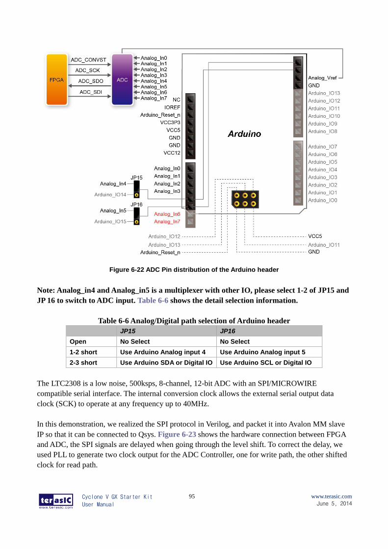
Cyclone V GX Starter Kit
User Manual
95
www.terasic.com
June 5, 2014
Figure 6-22 ADC Pin distribution of the Arduino header
Note: Analog_in4 and Analog_in5 is a multiplexer with other IO, please select 1-2 of JP15 and
JP 16 to switch to ADC input. Table 6-6 shows the detail selection information.
Table 6-6 Analog/Digital path selection of Arduino header
JP15 JP16
Open No Select No Select
1-2 short Use Arduino Analog input 4 Use Arduino Analog input 5
2-3 short Use Arduino SDA or Digital IO Use Arduino SCL or Digital IO
The LTC2308 is a low noise, 500ksps, 8-channel, 12-bit ADC with an SPI/MICROWIRE
compatible serial interface. The internal conversion clock allows the external serial output data
clock (SCK) to operate at any frequency up to 40MHz.
In this demonstration, we realized the SPI protocol in Verilog, and packet it into Avalon MM slave
IP so that it can be connected to Qsys. Figure 6-23 shows the hardware connection between FPGA
and ADC, the SPI signals are delayed when going through the level shift. To correct the delay, we
used PLL to generate two clock output for the ADC Controller, one for write path, the other shifted
clock for read path.
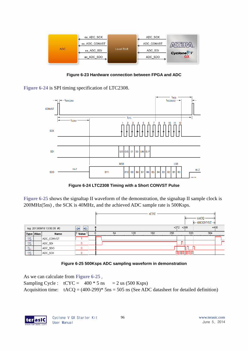
Cyclone V GX Starter Kit
User Manual
96
www.terasic.com
June 5, 2014
Figure 6-23 Hardware connection between FPGA and ADC
Figure 6-24 is SPI timing specification of LTC2308.
Figure 6-24 LTC2308 Timing with a Short CONVST Pulse
Figure 6-25 shows the signaltap II waveform of the demonstration, the signaltap II sample clock is
200MHz(5ns) , the SCK is 40MHz, and the achieved ADC sample rate is 500Ksps.
Figure 6-25 500Ksps ADC sampling waveform in demonstration
As we can calculate from Figure 6-25 ,
Sampling Cycle : tCYC = 400 * 5 ns = 2 us (500 Ksps)
Acquisition time: tACQ = (400-299)* 5ns = 505 ns (See ADC datasheet for detailed definition)
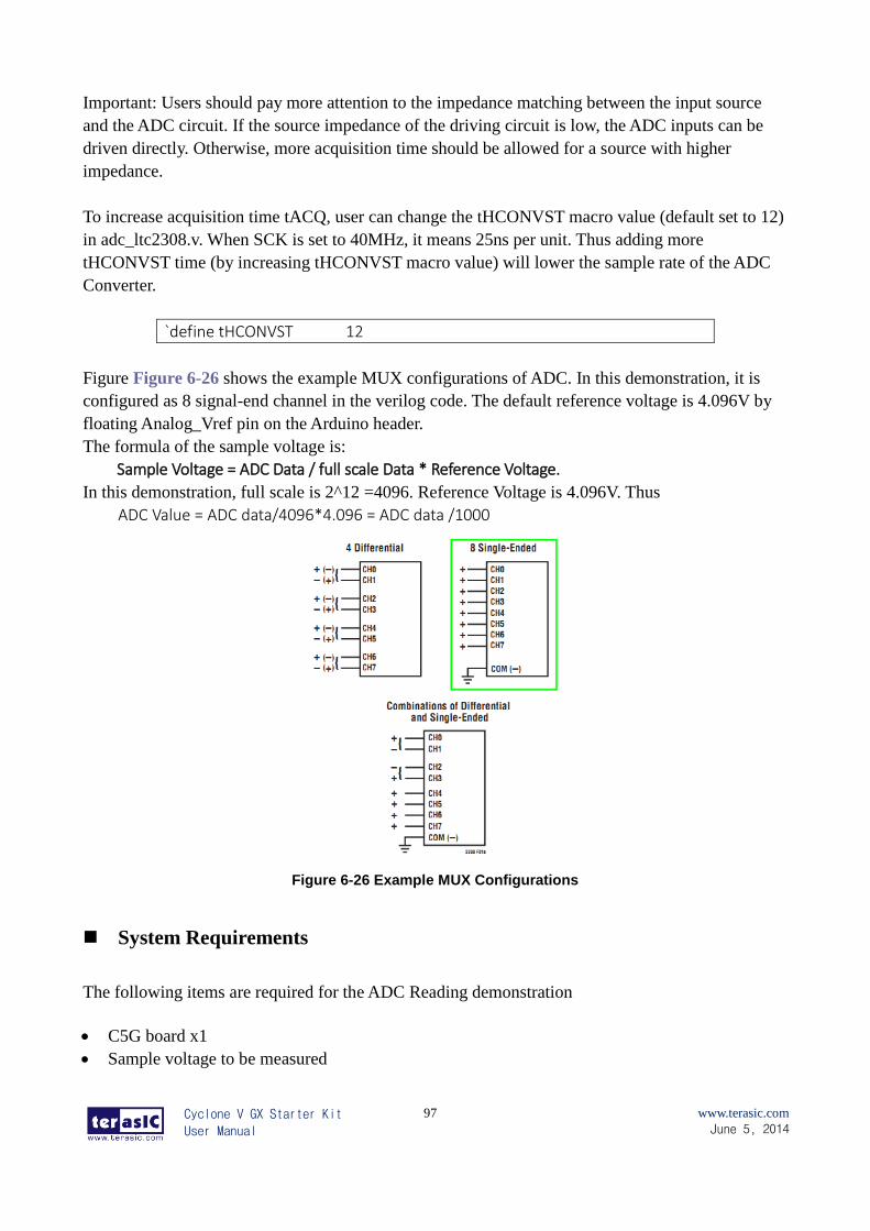
Cyclone V GX Starter Kit
User Manual
97
www.terasic.com
June 5, 2014
Important: Users should pay more attention to the impedance matching between the input source
and the ADC circuit. If the source impedance of the driving circuit is low, the ADC inputs can be
driven directly. Otherwise, more acquisition time should be allowed for a source with higher
impedance.
To increase acquisition time tACQ, user can change the tHCONVST macro value (default set to 12)
in adc_ltc2308.v. When SCK is set to 40MHz, it means 25ns per unit. Thus adding more
tHCONVST time (by increasing tHCONVST macro value) will lower the sample rate of the ADC
Converter.
`define tHCONVST 12
Figure Figure 6-26 shows the example MUX configurations of ADC. In this demonstration, it is
configured as 8 signal-end channel in the verilog code. The default reference voltage is 4.096V by
floating Analog_Vref pin on the Arduino header.
The formula of the sample voltage is:
Sample Voltage = ADC Data / full scale Data * Reference Voltage.
In this demonstration, full scale is 2^12 =4096. Reference Voltage is 4.096V. Thus
ADC Value = ADC data/4096*4.096 = ADC data /1000
Figure 6-26 Example MUX Configurations
System Requirements
The following items are required for the ADC Reading demonstration
C5G board x1
Sample voltage to be measured
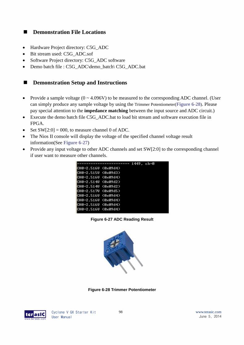
Cyclone V GX Starter Kit
User Manual
98
www.terasic.com
June 5, 2014
Demonstration File Locations
Hardware Project directory: C5G_ADC
Bit stream used: C5G_ADC.sof
Software Project directory: C5G_ADC software
Demo batch file : C5G_ADC\demo_batch\ C5G_ADC.bat
Demonstration Setup and Instructions
Provide a sample voltage (0 ~ 4.096V) to be measured to the corresponding ADC channel. (User
can simply produce any sample voltage by using the Trimmer Potentiometer(Figure 6-28). Please
pay special attention to the impedance matching between the input source and ADC circuit.)
Execute the demo batch file C5G_ADC.bat to load bit stream and software execution file in
FPGA.
Set SW[2:0] = 000, to measure channel 0 of ADC.
The Nios II console will display the voltage of the specified channel voltage result
information(See Figure 6-27)
Provide any input voltage to other ADC channels and set SW[2:0] to the corresponding channel
if user want to measure other channels.
Figure 6-27 ADC Reading Result
Figure 6-28 Trimmer Potentiometer
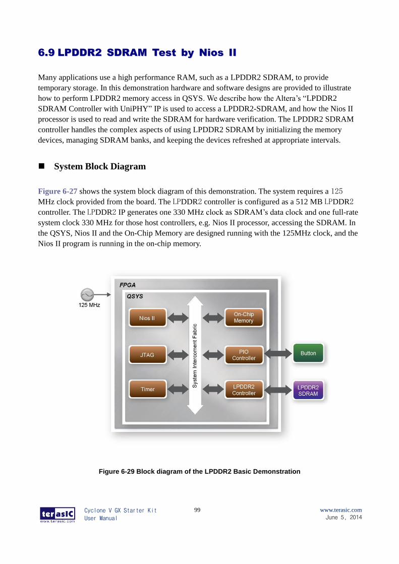
Cyclone V GX Starter Kit
User Manual
99
www.terasic.com
June 5, 2014
66..99 LLPPDDDDRR22 SSDDRRAAMM TTeesstt bbyy NNiiooss IIII
Many applications use a high performance RAM, such as a LPDDR2 SDRAM, to provide
temporary storage. In this demonstration hardware and software designs are provided to illustrate
how to perform LPDDR2 memory access in QSYS. We describe how the Altera’s “LPDDR2
SDRAM Controller with UniPHY” IP is used to access a LPDDR2-SDRAM, and how the Nios II
processor is used to read and write the SDRAM for hardware verification. The LPDDR2 SDRAM
controller handles the complex aspects of using LPDDR2 SDRAM by initializing the memory
devices, managing SDRAM banks, and keeping the devices refreshed at appropriate intervals.
System Block Diagram
Figure 6-27 shows the system block diagram of this demonstration. The system requires a 125
MHz clock provided from the board. The LPDDR2 controller is configured as a 512 MB LPDDR2
controller. The LPDDR2 IP generates one 330 MHz clock as SDRAM’s data clock and one full-rate
system clock 330 MHz for those host controllers, e.g. Nios II processor, accessing the SDRAM. In
the QSYS, Nios II and the On-Chip Memory are designed running with the 125MHz clock, and the
Nios II program is running in the on-chip memory.
Figure 6-29 Block diagram of the LPDDR2 Basic Demonstration
Cyclone V GX Starter Kit
User Manual
100
www.terasic.com
June 5, 2014
The system flow is controlled by a Nios II program. First, the Nios II program writes test patterns
into the whole 512MB of SDRAM. Then, it calls Nios II system function, alt_dcache_flush_all, to
make sure all data has been written to SDRAM. Finally, it reads data from SDRAM for data
verification. The program will show progress in JTAG-Terminal when writing/reading data to/from
the SDRAM. When verification process is completed, the result is displayed in the JTAG-Terminal.
Altera LPDDR2 SDRAM Controller with UniPHY
To use Altera LPDDR2 controller, users need to perform the four major steps:
1. Create correct pin assignments for the LPDDR2.
2. Setup correct parameters in LPDDR2 controller dialog.
3. Perform “Analysis and Synthesis” by selecting from the Quartus II menu:
ProcessStartStart Analysis & Synthesis.
4. Run the TCL files generated by LPDDR2 IP by selecting from the Quartus II menu:
ToolsTCL Scripts…
Design Tools
Quartus II 13.1
Nios II Eclipse 13.1
Demonstration Source Code
Quartus Project directory: C5G_LPDDR2_Nios_Test
Nios II Eclipse: C5G_LPDDR2_Nios_Test\Software
Nios II Project Compilation
Before you attempt to compile the reference design under Nios II Eclipse, make sure the project is
cleaned first by clicking ‘Clean’ from the ‘Project’ menu of Nios II Eclipse.
Demonstration Batch File
Demo Batch File Folder:
C5G_LPDDR2_Nios_Test\demo_batch
The demo batch file includes following files:
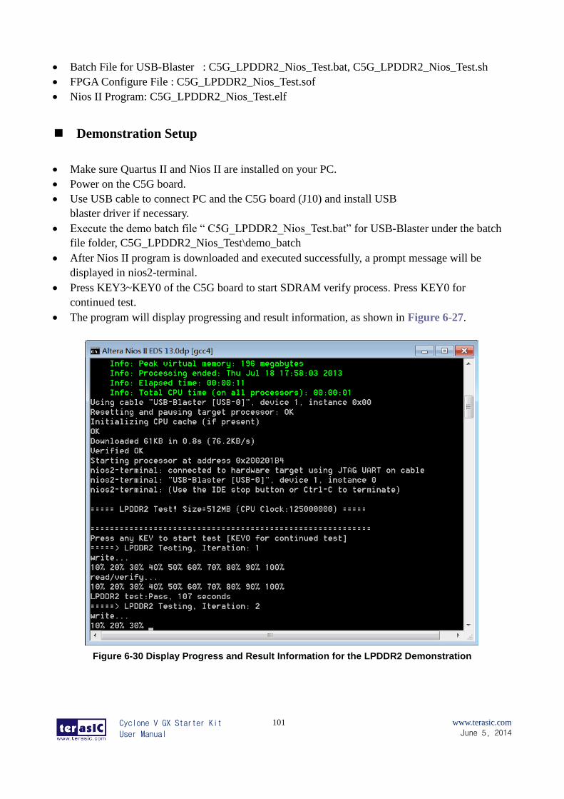
Cyclone V GX Starter Kit
User Manual
101
www.terasic.com
June 5, 2014
Batch File for USB-Blaster : C5G_LPDDR2_Nios_Test.bat, C5G_LPDDR2_Nios_Test.sh
FPGA Configure File : C5G_LPDDR2_Nios_Test.sof
Nios II Program: C5G_LPDDR2_Nios_Test.elf
Demonstration Setup
Make sure Quartus II and Nios II are installed on your PC.
Power on the C5G board.
Use USB cable to connect PC and the C5G board (J10) and install USB
blaster driver if necessary.
Execute the demo batch file “ C5G_LPDDR2_Nios_Test.bat” for USB-Blaster under the batch
file folder, C5G_LPDDR2_Nios_Test\demo_batch
After Nios II program is downloaded and executed successfully, a prompt message will be
displayed in nios2-terminal.
Press KEY3~KEY0 of the C5G board to start SDRAM verify process. Press KEY0 for
continued test.
The program will display progressing and result information, as shown in Figure 6-27.
Figure 6-30 Display Progress and Result Information for the LPDDR2 Demonstration
Cyclone V GX Starter Kit
User Manual
102
www.terasic.com
June 5, 2014
Additional Information
GGeettttiinngg HHeellpp
Here are the addresses where you can get help if you encounter problems:
Terasic Technologies
9F., No.176, Sec.2, Gongdao 5th Rd,
East Dist, HsinChu City, 30070. Taiwan, 30070
Email: [email protected]
Web: www.terasic.com
Cyclone V GX Starter Kit Web: www.C5G.terasic.com
RReevviissiioonn HHiissttoorryy
Date Version Changes
2013.08.09 First publication
2013.11.29 V1.01 Update for Revision B Hardware.
2014.04.07 V1.02 1. Fix Table 3-13 HDMI_TX_HS and
HDMI_TX_VS Description.
2. Add ADC components described
in Chapter 1.3