Cyclone V Device Overview - Mouser · PDF file• Variable-precision digital signal ......
29
Cyclone V Device Overview 2012.12.28 CV-51001 Subscribe Feedback The Cyclone ® V devices are designed to simultaneously accommodate the shrinking power consumption, cost, and time-to-market requirements; and the increasing bandwidth requirements for high-volume and cost-sensitive applications. Enhanced with integrated transceivers and hard memory controllers, the Cyclone V devices are suitable for applications in the industrial, wireless and wireline, military, and automotive markets. Key Advantages of Cyclone V Devices Table 1: Key Advantages of the Cyclone V Device Family Supporting Feature Advantage • Built on TSMC's 28 nm low-power (28LP) process technology and includes an abundance of hard intellectual property (IP) blocks • Up to 40% lower power consumption than the previous generation device Lower power consumption • 8-input adaptive logic module (ALM) • Up to 13.59 megabits (Mb) of embedded memory • Variable-precision digital signal processing (DSP) blocks Improved logic integration and differentiation capabilities • 3.125 gigabits per second (Gbps) and 5 Gbps transceivers • Hard memory controllers Increased bandwidth capacity • Tight integration of a dual-core ARM Cortex-A9 MPCore processor, hard IP, and an FPGA in a single Cyclone V system-on-a-chip (SoC) FPGA • Supports over 128 Gbps peak bandwidth with integrated data coherency between the processor and the FPGA fabric Hard processor system (HPS) with integrated ARM ® Cortex ™ -A9 MPCore processor • Requires only two core voltages to operate • Available in low-cost wirebond packaging • Includes innovative features such as Configuration via Protocol (CvP) and partial reconfiguration Lowest system cost ISO 9001:2008 Registered © 2012 Altera Corporation. All rights reserved. ALTERA, ARRIA, CYCLONE, HARDCOPY, MAX, MEGACORE, NIOS, QUARTUS and STRATIX words and logos are trademarks of Altera Corporation and registered in the U.S. Patent and Trademark Office and in other countries. All other words and logos identified as trademarks or service marks are the property of their respective holders as described at www.altera.com/common/legal.html. Altera warrants performance of its semiconductor products to current specifications in accordance with Altera's standard warranty, but reserves the right to make changes to any products and services at any time without notice. Altera assumes no responsibility or liability arising out of the application or use of any information, product, or service described herein except as expressly agreed to in writing by Altera. Altera customers are advised to obtain the latest version of device specifications before relying on any published information and before placing orders for products or services. www.altera.com 101 Innovation Drive, San Jose, CA 95134
Transcript of Cyclone V Device Overview - Mouser · PDF file• Variable-precision digital signal ......
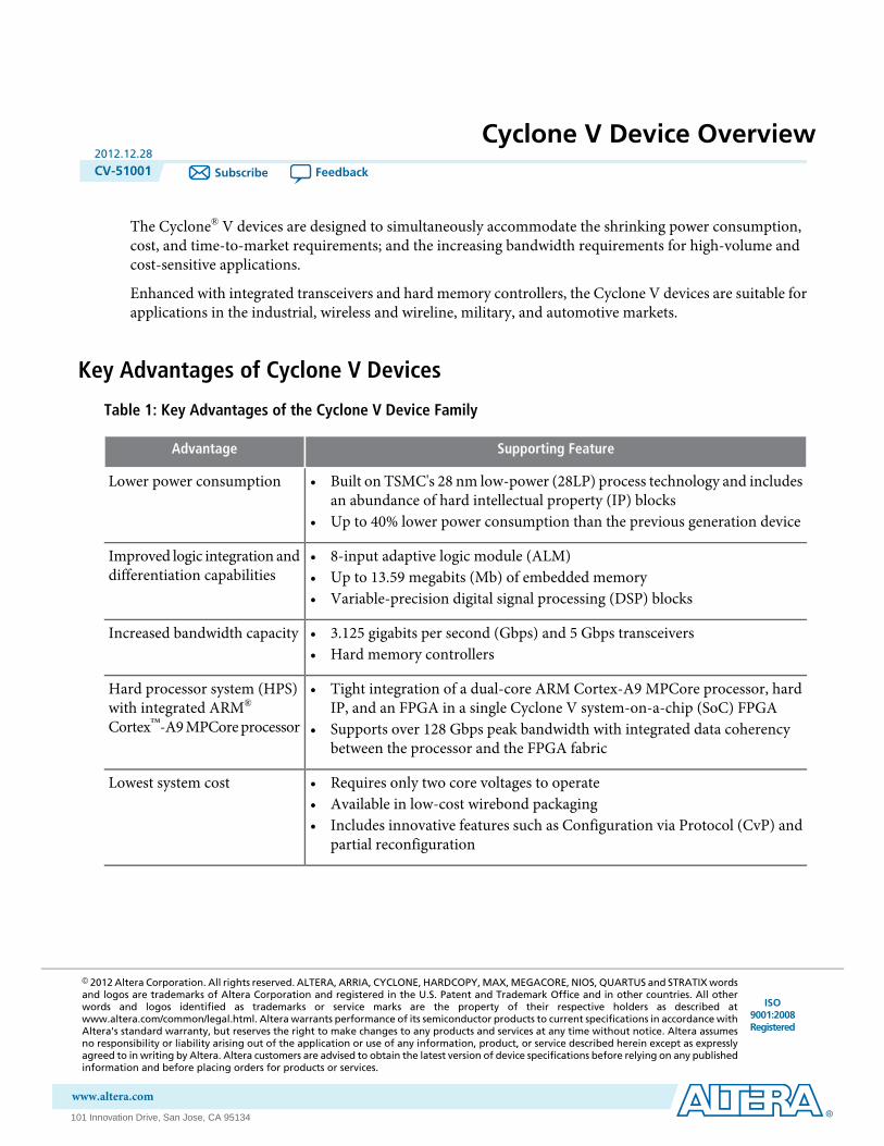
Cyclone V Device Overview2012.12.28
CV-51001 Subscribe Feedback
The Cyclone® V devices are designed to simultaneously accommodate the shrinking power consumption,cost, and time-to-market requirements; and the increasing bandwidth requirements for high-volume andcost-sensitive applications.
Enhanced with integrated transceivers and hard memory controllers, the Cyclone V devices are suitable forapplications in the industrial, wireless and wireline, military, and automotive markets.
Key Advantages of Cyclone V Devices
Table 1: Key Advantages of the Cyclone V Device Family
Supporting FeatureAdvantage
• Built on TSMC's 28 nm low-power (28LP) process technology and includesan abundance of hard intellectual property (IP) blocks
• Up to 40% lower power consumption than the previous generation device
Lower power consumption
• 8-input adaptive logic module (ALM)• Up to 13.59 megabits (Mb) of embedded memory• Variable-precision digital signal processing (DSP) blocks
Improved logic integration anddifferentiation capabilities
• 3.125 gigabits per second (Gbps) and 5 Gbps transceivers• Hard memory controllers
Increased bandwidth capacity
• Tight integration of a dual-core ARM Cortex-A9 MPCore processor, hardIP, and an FPGA in a single Cyclone V system-on-a-chip (SoC) FPGA
• Supports over 128 Gbps peak bandwidth with integrated data coherencybetween the processor and the FPGA fabric
Hard processor system (HPS)with integrated ARM®
Cortex™-A9MPCoreprocessor
• Requires only two core voltages to operate• Available in low-cost wirebond packaging• Includes innovative features such as Configuration via Protocol (CvP) and
partial reconfiguration
Lowest system cost
ISO9001:2008Registered
© 2012 Altera Corporation. All rights reserved. ALTERA, ARRIA, CYCLONE, HARDCOPY, MAX, MEGACORE, NIOS, QUARTUS and STRATIX wordsand logos are trademarks of Altera Corporation and registered in the U.S. Patent and Trademark Office and in other countries. All otherwords and logos identified as trademarks or service marks are the property of their respective holders as described atwww.altera.com/common/legal.html. Altera warrants performance of its semiconductor products to current specifications in accordance withAltera's standard warranty, but reserves the right to make changes to any products and services at any time without notice. Altera assumesno responsibility or liability arising out of the application or use of any information, product, or service described herein except as expresslyagreed to in writing by Altera. Altera customers are advised to obtain the latest version of device specifications before relying on any publishedinformation and before placing orders for products or services.
www.altera.com
101 Innovation Drive, San Jose, CA 95134
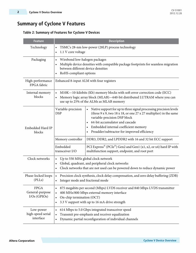
Summary of Cyclone V Features
Table 2: Summary of Features for Cyclone V Devices
DescriptionFeature
• TSMC's 28-nm low-power (28LP) process technology• 1.1 V core voltage
Technology
• Wirebond low-halogen packages• Multiple device densities with compatible package footprints for seamless migration
between different device densities• RoHS-compliant options
Packaging
Enhanced 8-input ALM with four registersHigh-performanceFPGA fabric
• M10K—10-kilobits (Kb) memory blocks with soft error correction code (ECC)• Memory logic array block (MLAB)—640-bit distributed LUTRAM where you can
use up to 25% of the ALMs as MLAB memory
Internal memoryblocks
• Native support for up to three signal processing precision levels(three 9 x 9, two 18 x 18, or one 27 x 27 multiplier) in the samevariable-precision DSP block
• 64-bit accumulator and cascade• Embedded internal coefficient memory• Preadder/subtractor for improved efficiency
Variable-precisionDSP
Embedded Hard IPblocks
DDR3, DDR2, and LPDDR2 with 16 and 32 bit ECC supportMemory controller
PCI Express® (PCIe®) Gen2 and Gen1 (x1, x2, or x4) hard IP withmultifunction support, endpoint, and root port
Embeddedtransceiver I/O
• Up to 550 MHz global clock network• Global, quadrant, and peripheral clock networks• Clock networks that are not used can be powered down to reduce dynamic power
Clock networks
• Precision clock synthesis, clock delay compensation, and zero delay buffering (ZDB)• Integer mode and fractional mode
Phase-locked loops(PLLs)
• 875 megabits per second (Mbps) LVDS receiver and 840 Mbps LVDS transmitter• 400 MHz/800 Mbps external memory interface• On-chip termination (OCT)• 3.3 V support with up to 16 mA drive strength
FPGAGeneral-purposeI/Os (GPIOs)
• 614 Mbps to 5.0 Gbps integrated transceiver speed• Transmit pre-emphasis and receiver equalization• Dynamic partial reconfiguration of individual channels
Low-powerhigh-speed serial
interface
Cyclone V Device OverviewAltera Corporation
CV-51001Cyclone V Device Overview2 2012.12.28
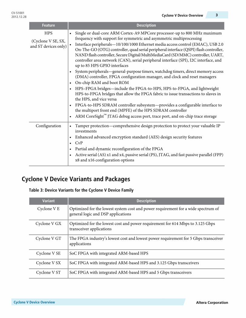
DescriptionFeature
• Single or dual-core ARM Cortex-A9 MPCore processor-up to 800 MHz maximumfrequency with support for symmetric and asymmetric multiprocessing
• Interface peripherals—10/100/1000 Ethernet media access control (EMAC), USB 2.0On-The-GO (OTG) controller, quad serial peripheral interface (QSPI) flash controller,NANDflash controller, SecureDigital/MultiMediaCard (SD/MMC) controller,UART,controller area network (CAN), serial peripheral interface (SPI), I2C interface, andup to 85 HPS GPIO interfaces
• System peripherals—general-purpose timers, watchdog timers, directmemory access(DMA) controller, FPGA configuration manager, and clock and reset managers
• On-chip RAM and boot ROM• HPS–FPGA bridges—include the FPGA-to-HPS, HPS-to-FPGA, and lightweight
HPS-to-FPGA bridges that allow the FPGA fabric to issue transactions to slaves inthe HPS, and vice versa
• FPGA-to-HPS SDRAM controller subsystem—provides a configurable interface tothe multiport front end (MPFE) of the HPS SDRAM controller
• ARM CoreSight™ JTAG debug access port, trace port, and on-chip trace storage
HPS
(Cyclone V SE, SX,and ST devices only)
• Tamper protection—comprehensive design protection to protect your valuable IPinvestments
• Enhanced advanced encryption standard (AES) design security features• CvP• Partial and dynamic reconfiguration of the FPGA• Active serial (AS) x1 and x4, passive serial (PS), JTAG, and fast passive parallel (FPP)
x8 and x16 configuration options
Configuration
Cyclone V Device Variants and Packages
Table 3: Device Variants for the Cyclone V Device Family
DescriptionVariant
Optimized for the lowest system cost and power requirement for a wide spectrum ofgeneral logic and DSP applications
Cyclone V E
Optimized for the lowest cost and power requirement for 614 Mbps to 3.125 Gbpstransceiver applications
Cyclone V GX
The FPGA industry’s lowest cost and lowest power requirement for 5 Gbps transceiverapplications
Cyclone V GT
SoC FPGA with integrated ARM-based HPSCyclone V SE
SoC FPGA with integrated ARM-based HPS and 3.125 Gbps transceiversCyclone V SX
SoC FPGA with integrated ARM-based HPS and 5 Gbps transceiversCyclone V ST
Altera CorporationCyclone V Device Overview
3Cyclone V Device OverviewCV-510012012.12.28
Cyclone V EThis section provides the available options,maximum resource counts, and package plan for the CycloneVEdevices.
Available Options
Figure 1: Sample Ordering Code and Available Options for Cyclone V E Devices—Preliminary
Family Signature
Embedded Hard IPs
Package Type
Package Code
Operating Temperature
FPGA Fabric Speed Grade
Optional SuffixIndicates specific deviceoptions or shipment method
E : Enhanced logic/memory
B : No hard PCIe or hardmemory controller
F : No hard PCIe and maximum2 hard memory controllers
5C : Cyclone V
F : FineLine BGA (FBGA)U : Ultra FineLine BGA (UBGA)M : Micro FineLine BGA (MBGA)
FBGA Package Type17 : 256 pins23 : 484 pins27 : 672 pins31 : 896 pinsUBGA Package Type15 : 324 pins19 : 484 pinsMBGA Package Type13 : 386 pins15 : 484 pins
C : Commercial (TJ = 0° C to 85° C)I : Industrial (TJ = -40° C to 100° C)A : Automotive (TJ = -40° C to 125° C)
6 (fastest)78
N : Lead-free packagingES : Engineering sample
5C E F A9 F 31 C 7 N
Member Code
Family Variant
A2 : 25K logic elementsA4 : 49K logic elementsA5 : 77K logic elementsA7 : 149.5K logic elementsA9 : 301K logic elements
Maximum Resources
Table 4: Maximum Resource Counts for Cyclone V E Devices—Preliminary
Member CodeResource
A9A7A5A4A2
301149.5774925Logic Elements (LE) (K)
113,56056,48029,08018,4809,434ALM
454,240225,920116,32073,92037,736Register
12,2006,8604,4603,0801,760M10KMemory (Kb)
1,717836424303196MLAB
3421561506625Variable-precision DSP Block
6843123001325018 x 18 Multiplier
87644PLL
480480240224224GPIO1
1 The number of GPIOs does not include transceiver I/Os. In the Quartus II software, the number of user I/Osincludes transceiver I/Os.
Cyclone V Device OverviewAltera Corporation
CV-51001Cyclone V Device Overview4 2012.12.28
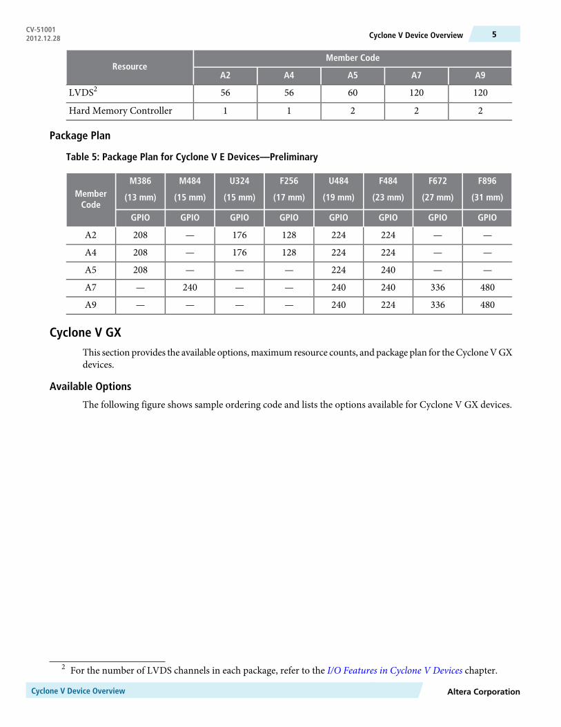
Member CodeResource
A9A7A5A4A2
120120605656LVDS2
22211Hard Memory Controller
Package Plan
Table 5: Package Plan for Cyclone V E Devices—Preliminary
F896
(31 mm)
F672
(27 mm)
F484
(23 mm)
U484
(19 mm)
F256
(17 mm)
U324
(15 mm)
M484
(15 mm)
M386
(13 mm)MemberCode
GPIOGPIOGPIOGPIOGPIOGPIOGPIOGPIO
——224224128176—208A2
——224224128176—208A4
——240224———208A5
480336240240——240—A7
480336224240————A9
Cyclone V GXThis section provides the available options,maximumresource counts, and package plan for theCycloneVGXdevices.
Available Options
The following figure shows sample ordering code and lists the options available for Cyclone V GX devices.
2 For the number of LVDS channels in each package, refer to the I/O Features in Cyclone V Devices chapter.
Altera CorporationCyclone V Device Overview
5Cyclone V Device OverviewCV-510012012.12.28
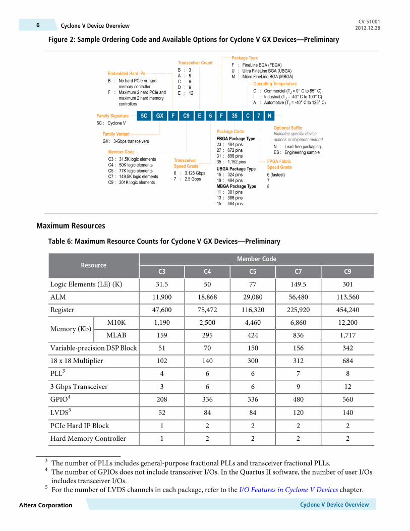
Figure 2: Sample Ordering Code and Available Options for Cyclone V GX Devices—Preliminary
Family Signature
Embedded Hard IPs
Transceiver Count
TransceiverSpeed Grade
Package Type
Package Code
Operating Temperature
FPGA FabricSpeed Grade
Optional SuffixIndicates specific deviceoptions or shipment methodGX : 3-Gbps transceivers
B : No hard PCIe or hardmemory controller
F : Maximum 2 hard PCIe andmaximum 2 hard memorycontrollers
5C : Cyclone V
C3 : 31.5K logic elementsC4 : 50K logic elementsC5 : 77K logic elementsC7 : 149.5K logic elementsC9 : 301K logic elements
B : 3A : 5C : 6D : 9E : 12
6 : 3.125 Gbps7 : 2.5 Gbps
F : FineLine BGA (FBGA)U : Ultra FineLine BGA (UBGA)M : Micro FineLine BGA (MBGA)
FBGA Package Type23 : 484 pins27 : 672 pins31 : 896 pins35 : 1,152 pinsUBGA Package Type15 : 324 pins19 : 484 pinsMBGA Package Type11 : 301 pins13 : 386 pins15 : 484 pins
C : Commercial (TJ = 0° C to 85° C)I : Industrial (TJ = -40° C to 100° C)A : Automotive (TJ = -40° C to 125° C)
6 (fastest)78
N : Lead-free packagingES : Engineering sample
5C GX F C9 E 6 F 35 C 7 N
Member Code
Family Variant
Maximum Resources
Table 6: Maximum Resource Counts for Cyclone V GX Devices—Preliminary
Member CodeResource
C9C7C5C4C3
301149.5775031.5Logic Elements (LE) (K)
113,56056,48029,08018,86811,900ALM
454,240225,920116,32075,47247,600Register
12,2006,8604,4602,5001,190M10KMemory (Kb)
1,717836424295159MLAB
3421561507051Variable-precisionDSPBlock
68431230014010218 x 18 Multiplier
87664PLL3
1296633 Gbps Transceiver
560480336336208GPIO4
140120848452LVDS5
22221PCIe Hard IP Block
22221Hard Memory Controller
3 The number of PLLs includes general-purpose fractional PLLs and transceiver fractional PLLs.4 The number of GPIOs does not include transceiver I/Os. In the Quartus II software, the number of user I/Os
includes transceiver I/Os.5 For the number of LVDS channels in each package, refer to the I/O Features in Cyclone V Devices chapter.
Cyclone V Device OverviewAltera Corporation
CV-51001Cyclone V Device Overview6 2012.12.28
Package Plan
Table 7: Package Plan for Cyclone V GX Devices—Preliminary
F1152
(35 mm)
F896
(31 mm)
F672
(27 mm)
F484
(23 mm)
U484
(19 mm)
U324
(15 mm)
M484
(15 mm)
M386
(13 mm)
M301
(11 mm)Mem-berCode
XCVRGPIOXCVRGPIOXCVRGPIOXCVRGPIOXCVRGPIOXCVRGPIOXCVRGPIOXCVRGPIOXCVRGPIO
——————320832083144——————C3
————633662406224————61754127C4
————633662406224————61754127C5
——9480933662406240——3240————C7
1256012480933662245240————————C9
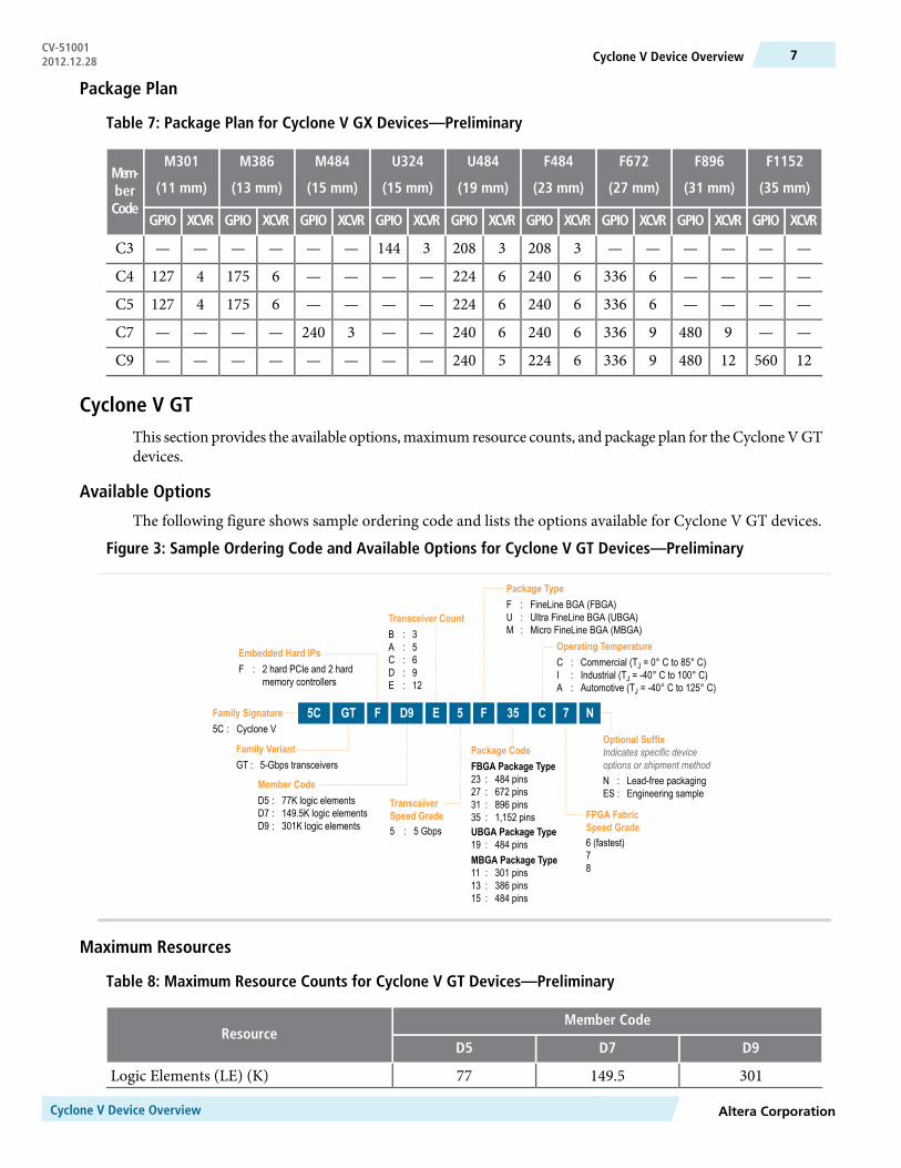
Cyclone V GTThis section provides the available options,maximumresource counts, and package plan for theCycloneVGTdevices.
Available Options
The following figure shows sample ordering code and lists the options available for Cyclone V GT devices.
Figure 3: Sample Ordering Code and Available Options for Cyclone V GT Devices—Preliminary
Family Signature
Embedded Hard IPs
Transceiver Count
TransceiverSpeed Grade
Package Type
Package Code
Operating Temperature
FPGA FabricSpeed Grade
Optional SuffixIndicates specific deviceoptions or shipment methodGT : 5-Gbps transceivers
F : 2 hard PCIe and 2 hardmemory controllers
5C : Cyclone V
D5 : 77K logic elementsD7 : 149.5K logic elementsD9 : 301K logic elements
B : 3A : 5C : 6D : 9E : 12
5 : 5 Gbps
F : FineLine BGA (FBGA)U : Ultra FineLine BGA (UBGA)M : Micro FineLine BGA (MBGA)
FBGA Package Type23 : 484 pins27 : 672 pins31 : 896 pins35 : 1,152 pinsUBGA Package Type19 : 484 pinsMBGA Package Type11 : 301 pins13 : 386 pins15 : 484 pins
C : Commercial (TJ = 0° C to 85° C)I : Industrial (TJ = -40° C to 100° C)A : Automotive (TJ = -40° C to 125° C)
6 (fastest)78
N : Lead-free packagingES : Engineering sample
5C GT F D9 E 5 F 35 C 7 N
Member Code
Family Variant
Maximum Resources
Table 8: Maximum Resource Counts for Cyclone V GT Devices—Preliminary
Member CodeResource
D9D7D5
301149.577Logic Elements (LE) (K)
Altera CorporationCyclone V Device Overview
7Cyclone V Device OverviewCV-510012012.12.28
Member CodeResource
D9D7D5
113,56056,48029,080ALM
454,240225,920116,320Register
12,2006,8604,460M10KMemory (Kb)
1,717836424MLAB
342156150Variable-precision DSP Block
68431230018 x 18 Multiplier
876PLL6
12965 Gbps Transceiver
560480336GPIO7
14012084LVDS8
222PCIe Hard IP Block
222Hard Memory Controller
Package Plan
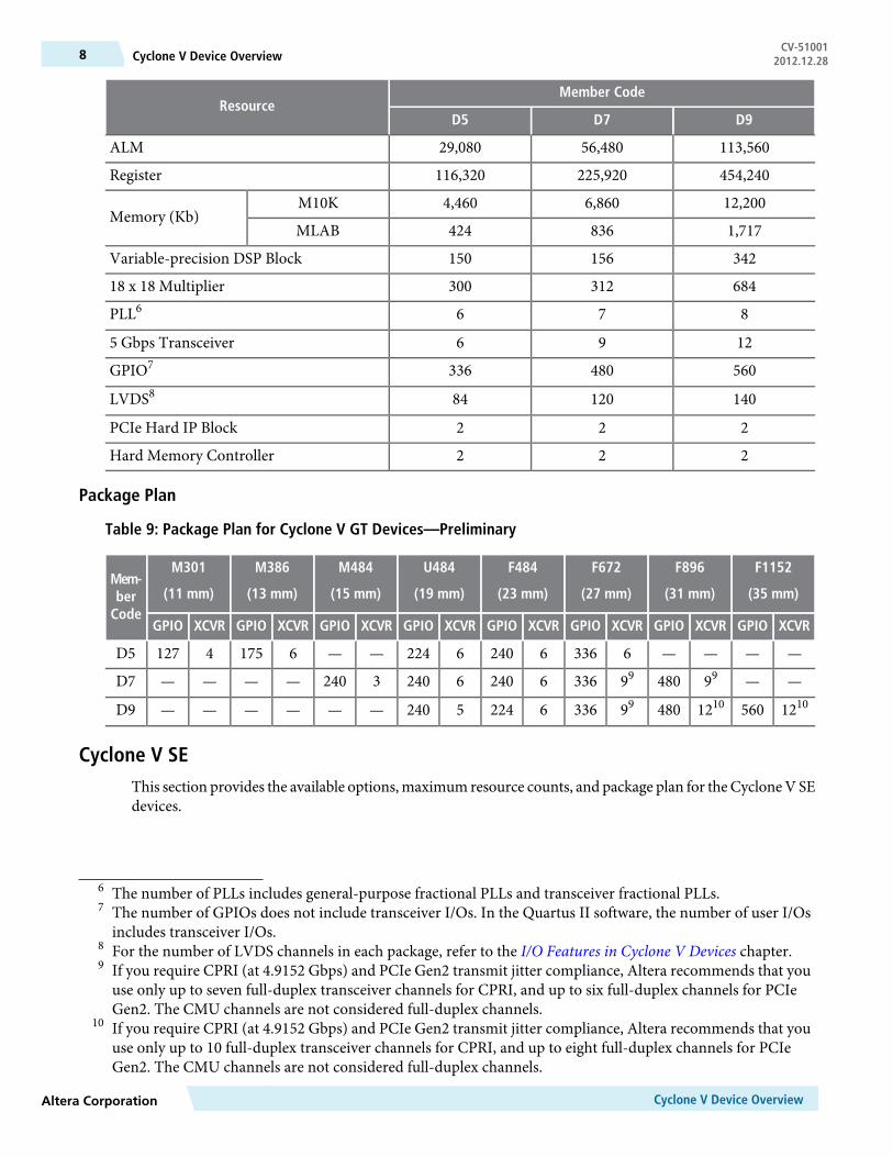
Table 9: Package Plan for Cyclone V GT Devices—Preliminary
F1152
(35 mm)
F896
(31 mm)
F672
(27 mm)
F484
(23 mm)
U484
(19 mm)
M484
(15 mm)
M386
(13 mm)
M301
(11 mm)Mem-ber
CodeXCVRGPIOXCVRGPIOXCVRGPIOXCVRGPIOXCVRGPIOXCVRGPIOXCVRGPIOXCVRGPIO
————633662406224——61754127D5
——9948099336624062403240————D7
121056012104809933662245240——————D9
Cyclone V SEThis section provides the available options,maximum resource counts, and package plan for theCycloneV SEdevices.
6 The number of PLLs includes general-purpose fractional PLLs and transceiver fractional PLLs.7 The number of GPIOs does not include transceiver I/Os. In the Quartus II software, the number of user I/Os
includes transceiver I/Os.8 For the number of LVDS channels in each package, refer to the I/O Features in Cyclone V Devices chapter.9 If you require CPRI (at 4.9152 Gbps) and PCIe Gen2 transmit jitter compliance, Altera recommends that you
use only up to seven full-duplex transceiver channels for CPRI, and up to six full-duplex channels for PCIeGen2. The CMU channels are not considered full-duplex channels.
10 If you require CPRI (at 4.9152 Gbps) and PCIe Gen2 transmit jitter compliance, Altera recommends that youuse only up to 10 full-duplex transceiver channels for CPRI, and up to eight full-duplex channels for PCIeGen2. The CMU channels are not considered full-duplex channels.
Cyclone V Device OverviewAltera Corporation
CV-51001Cyclone V Device Overview8 2012.12.28
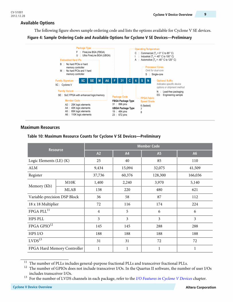
Available Options
The following figure shows sample ordering code and lists the options available for Cyclone V SE devices.
Figure 4: Sample Ordering Code and Available Options for Cyclone V SE Devices—Preliminary
Family Signature
Embedded Hard IPs
Package Type
Package Code
Operating Temperature
FPGA FabricSpeed Grade
Optional SuffixIndicates specific deviceoptions or shipment method
SE : SoC FPGA with enhanced logic/memory
5C : Cyclone V
F : FineLine BGA (FBGA)U : Ultra FineLine BGA (UBGA)
FBGA Package Type31 : 896 pinsUBGA Package Type19 : 484 pins23 : 672 pins
C : Commercial (TJ = 0° C to 85° C)I : Industrial (TJ = -40° C to 100° C)A : Automotive (TJ = -40° C to 125° C)
6 (fastest)78
Processor CoresOmit for dual-coreS : Single-core
N : Lead-free packagingES : Engineering sample
5C SE M A6 F 31 C 6 S N
Member Code
Family Variant
A2 : 25K logic elementsA4 : 40K logic elementsA5 : 85K logic elementsA6 : 110K logic elements
B : No hard PCIe or hardmemory controller
M : No hard PCIe and 1 hardmemory controller
Maximum Resources
Table 10: Maximum Resource Counts for Cyclone V SE Devices—Preliminary
Member CodeResource
A6A5A4A2
110854025Logic Elements (LE) (K)
41,50932,07515,0949,434ALM
166,036128,30060,37637,736Register
5,1403,9702,2401,400M10KMemory (Kb)
621480220138MLAB
112875836Variable-precision DSP Block
2241741167218 x 18 Multiplier
6654FPGA PLL11
3333HPS PLL
288288145145FPGA GPIO12
188188188188HPS I/O
72723131LVDS13
1111FPGA Hard Memory Controller
11 The number of PLLs includes general-purpose fractional PLLs and transceiver fractional PLLs.12 The number of GPIOs does not include transceiver I/Os. In the Quartus II software, the number of user I/Os
includes transceiver I/Os.13 For the number of LVDS channels in each package, refer to the I/O Features in Cyclone V Devices chapter.
Altera CorporationCyclone V Device Overview
9Cyclone V Device OverviewCV-510012012.12.28
Member CodeResource
A6A5A4A2
1111HPS Hard Memory Controller
Single- or dual-coreSingle- or dual-coreSingle- ordual-core
Single- ordual-core
ARM Cortex-A9 MPCoreProcessor
Package Plan
Table 11: Package Plan for Cyclone V SE Devices—Preliminary
F896
(31 mm)
U672
(23 mm)
U484
(19 mm)Member Code
HPS I/OFPGA GPIOHPS I/OFPGA GPIOHPS I/OFPGA GPIO
——18814516166A2
——18814516166A4
18828818814516166A5
18828818814516166A6
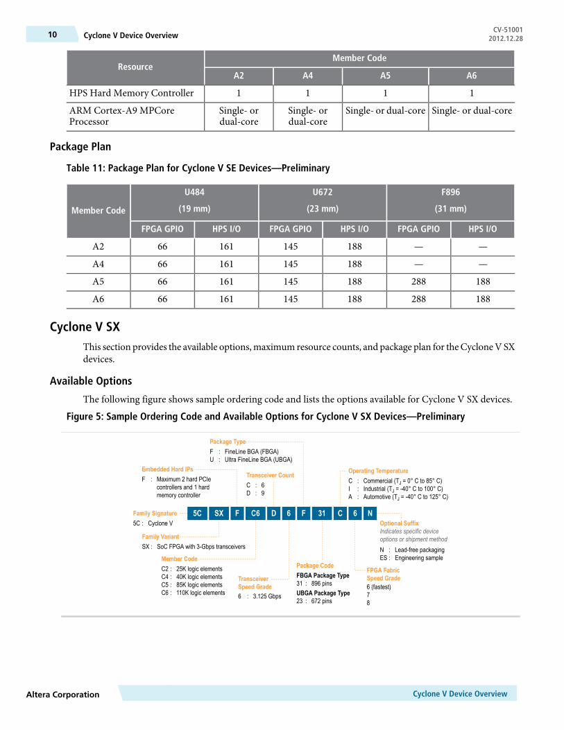
Cyclone V SXThis section provides the available options,maximum resource counts, and package plan for theCycloneV SXdevices.
Available Options
The following figure shows sample ordering code and lists the options available for Cyclone V SX devices.
Figure 5: Sample Ordering Code and Available Options for Cyclone V SX Devices—Preliminary
Family Signature
Embedded Hard IPsTransceiver Count
TransceiverSpeed Grade
Package Type
Package Code
Operating Temperature
FPGA FabricSpeed Grade
Optional SuffixIndicates specific deviceoptions or shipment method
SX : SoC FPGA with 3-Gbps transceivers
F : Maximum 2 hard PCIecontrollers and 1 hardmemory controller
5C : Cyclone V
C2 : 25K logic elementsC4 : 40K logic elementsC5 : 85K logic elementsC6 : 110K logic elements
C : 6D : 9
6 : 3.125 Gbps
F : FineLine BGA (FBGA)U : Ultra FineLine BGA (UBGA)
FBGA Package Type31 : 896 pinsUBGA Package Type23 : 672 pins
C : Commercial (TJ = 0° C to 85° C)I : Industrial (TJ = -40° C to 100° C)A : Automotive (TJ = -40° C to 125° C)
6 (fastest)78
N : Lead-free packagingES : Engineering sample
5C SX F C6 D 6 F 31 C 6 N
Member Code
Family Variant
Cyclone V Device OverviewAltera Corporation
CV-51001Cyclone V Device Overview10 2012.12.28
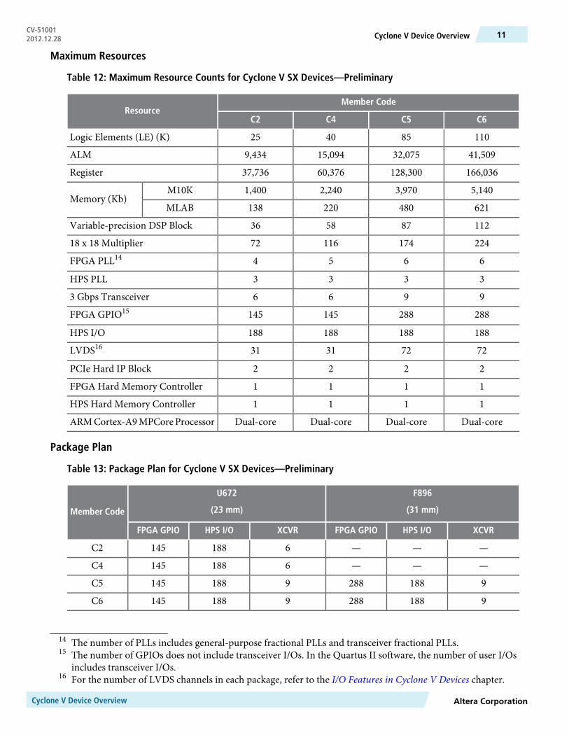
Maximum Resources
Table 12: Maximum Resource Counts for Cyclone V SX Devices—Preliminary
Member CodeResource
C6C5C4C2
110854025Logic Elements (LE) (K)
41,50932,07515,0949,434ALM
166,036128,30060,37637,736Register
5,1403,9702,2401,400M10KMemory (Kb)
621480220138MLAB
112875836Variable-precision DSP Block
2241741167218 x 18 Multiplier
6654FPGA PLL14
3333HPS PLL
99663 Gbps Transceiver
288288145145FPGA GPIO15
188188188188HPS I/O
72723131LVDS16
2222PCIe Hard IP Block
1111FPGA Hard Memory Controller
1111HPS Hard Memory Controller
Dual-coreDual-coreDual-coreDual-coreARMCortex-A9MPCore Processor
Package Plan
Table 13: Package Plan for Cyclone V SX Devices—Preliminary
F896
(31 mm)
U672
(23 mm)Member Code
XCVRHPS I/OFPGA GPIOXCVRHPS I/OFPGA GPIO
———6188145C2
———6188145C4
91882889188145C5
91882889188145C6
14 The number of PLLs includes general-purpose fractional PLLs and transceiver fractional PLLs.15 The number of GPIOs does not include transceiver I/Os. In the Quartus II software, the number of user I/Os
includes transceiver I/Os.16 For the number of LVDS channels in each package, refer to the I/O Features in Cyclone V Devices chapter.
Altera CorporationCyclone V Device Overview
11Cyclone V Device OverviewCV-510012012.12.28
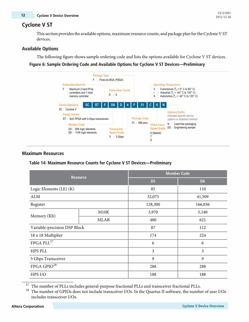
Cyclone V STThis section provides the available options,maximum resource counts, and package plan for theCycloneV STdevices.
Available Options
The following figure shows sample ordering code and lists the options available for Cyclone V ST devices.
Figure 6: Sample Ordering Code and Available Options for Cyclone V ST Devices—Preliminary
Family Signature
Embedded Hard IPs
Transceiver Count
TransceiverSpeed Grade
Package Type
Package Code
Operating Temperature
FPGA FabricSpeed Grade
Optional SuffixIndicates specific deviceoptions or shipment methodST : SoC FPGA with 5-Gbps transceivers
F : Maximum 2 hard PCIecontrollers and 1 hardmemory controller
5C : Cyclone V
D5 : 85K logic elementsD6 : 110K logic elements
D : 9
5 : 5 Gbps
F : FineLine BGA (FBGA)
31 : 896 pins
C : Commercial (TJ = 0° C to 85° C)I : Industrial (TJ = -40° C to 100° C)A : Automotive (TJ = -40° C to 125° C)
6 (fastest)78
N : Lead-free packagingES : Engineering sample
5C ST F D6 D 4 F 31 C 6 N
Member Code
Family Variant
Maximum Resources
Table 14: Maximum Resource Counts for Cyclone V ST Devices—Preliminary
Member CodeResource
D6D5
11085Logic Elements (LE) (K)
41,50932,075ALM
166,036128,300Register
5,1403,970M10KMemory (Kb)
621480MLAB
11287Variable-precision DSP Block
22417418 x 18 Multiplier
66FPGA PLL17
33HPS PLL
995 Gbps Transceiver
288288FPGA GPIO18
188188HPS I/O
17 The number of PLLs includes general-purpose fractional PLLs and transceiver fractional PLLs.18 The number of GPIOs does not include transceiver I/Os. In the Quartus II software, the number of user I/Os
includes transceiver I/Os.
Cyclone V Device OverviewAltera Corporation
CV-51001Cyclone V Device Overview12 2012.12.28
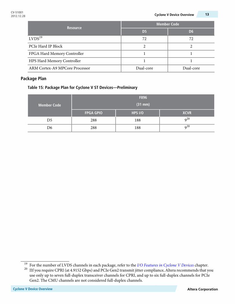
Member CodeResource
D6D5
7272LVDS19
22PCIe Hard IP Block
11FPGA Hard Memory Controller
11HPS Hard Memory Controller
Dual-coreDual-coreARM Cortex-A9 MPCore Processor
Package Plan
Table 15: Package Plan for Cyclone V ST Devices—Preliminary
F896
(31 mm)Member Code
XCVRHPS I/OFPGA GPIO
920188288D5
920188288D6
19 For the number of LVDS channels in each package, refer to the I/O Features in Cyclone V Devices chapter.20 IIf you require CPRI (at 4.9152 Gbps) and PCIe Gen2 transmit jitter compliance, Altera recommends that you
use only up to seven full-duplex transceiver channels for CPRI, and up to six full-duplex channels for PCIeGen2. The CMU channels are not considered full-duplex channels.
Altera CorporationCyclone V Device Overview
13Cyclone V Device OverviewCV-510012012.12.28
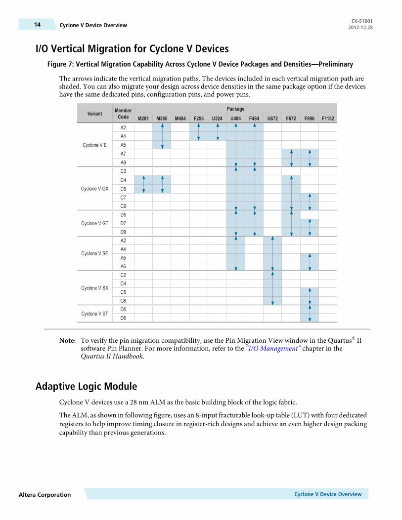
I/O Vertical Migration for Cyclone V DevicesFigure 7: Vertical Migration Capability Across Cyclone V Device Packages and Densities—Preliminary
The arrows indicate the vertical migration paths. The devices included in each vertical migration path areshaded. You can also migrate your design across device densities in the same package option if the deviceshave the same dedicated pins, configuration pins, and power pins.
Variant MemberCode
Package
M281 M385 M484 F256 U324 U484 F484 U672 F672 F896 F1152
Cyclone V E
A2A4A5A7A9
Cyclone V GX
C3C4C5C7C9
Cyclone V GTD5D7D9
Cyclone V SE
A2A4A5A6
Cyclone V SX
C2C4C5C6
Cyclone V STD5D6
To verify the pin migration compatibility, use the Pin Migration View window in the Quartus® IIsoftware Pin Planner. For more information, refer to the “I/O Management” chapter in theQuartus II Handbook.
Note:
Adaptive Logic ModuleCyclone V devices use a 28 nm ALM as the basic building block of the logic fabric.
The ALM, as shown in following figure, uses an 8-input fracturable look-up table (LUT) with four dedicatedregisters to help improve timing closure in register-rich designs and achieve an even higher design packingcapability than previous generations.
Cyclone V Device OverviewAltera Corporation
CV-51001Cyclone V Device Overview14 2012.12.28
Figure 8: ALM for Cyclone V Devices
FPGA Device
12345678
AdaptiveLUT
FullAdder
Reg
Reg
FullAdder
Reg
Reg
You can configure up to 25% of the ALMs in the Cyclone V devices as distributed memory using MLABs.For more information, refer to Embedded Memory Capacity in Cyclone V Devices on page standalone-17.
Variable-Precision DSP BlockCyclone V devices feature a variable-precision DSP block that supports these features:
• Configurable to support signal processing precisions ranging from 9 x 9, 18 x 18, 27 x 27, and 36 x 36bits natively
• A 64-bit accumulator• A hard preadder that is available in both 18- and 27-bit modes• Cascaded output adders for efficient systolic finite impulse response (FIR) filters• Internal coefficient register banks, 8 deep, for each multiplier in 18- or 27-bit mode• Fully independent multiplier operation• A second accumulator feedback register to accommodate complex multiply-accumulate functions• Efficient support for single-precision floating point arithmetic• The inferability of all modes by the Quartus II design software
Table 16: Variable-Precision DSP Block Configurations for Cyclone V Devices
DSP Block ResourceMultiplier Size (Bit)Usage Example
1Three 9 x 9Low precision fixed point for videoapplications
1Two 18 x 18Mediumprecision fixed point in FIRfilters
1Two 18 x 18 with accumulateFIR filters and general DSP usage
1One 27 x 27 with accumulateHigh precision fixed- orfloating-point implementations
Altera CorporationCyclone V Device Overview
15Cyclone V Device OverviewCV-510012012.12.28
You can configure each DSP block during compilation as independent three 9 x 9, two 18 x 18, or one 27 x 27multipliers. With a dedicated 64 bit cascade bus, you can cascade multiple variable-precision DSP blocks toimplement even higher precision DSP functions efficiently.
Table 17: Number of Multipliers in Cyclone V Devices
The table lists the variable-precision DSP resources by bit precision for each Cyclone V device.18 x 18
MultiplierAdder
Summedwith 36 bit
Input
18 x 18
MultiplierAdder Mode
Independent Input and Output
Multiplications OperatorVariable-pre-cision
DSP Block
MemberCode
Variant 27 x 27
Multiplier
18 x 18
Multiplier
9 x 9
Multiplier
252525507525A2
Cyclone V E
66666613219866A4
150150150300450150A5
156156156312468156A7
3423423426841,026342A9
51515110215351C3
Cyclone VGX
70707014021070C4
150150150300450150C5
156156156312468156C7
3423423426841,026342C9
150150150300450150D5Cyclone V
GT 156156156312468156D7
3423423426841,026342D9
3636367210836A2
Cyclone VSE
58585811617458A4
87878717426187A5
112112112224336112A6
3636367210836C2
Cyclone VSX
58585811617458C4
87878717426187C5
112112112224336112C6
87878717426187D5Cyclone VST 112112112224336112D6
Cyclone V Device OverviewAltera Corporation
CV-51001Cyclone V Device Overview16 2012.12.28
Embedded Memory BlocksThe embedded memory blocks in the devices are flexible and designed to provide an optimal amount ofsmall- and large-sized memory arrays to fit your design requirements.
Types of Embedded MemoryThe Cyclone V devices contain two types of memory blocks:
• 10 Kb M10K blocks blocks—blocks of dedicated memory resources. The M10K blocks blocks are idealfor larger memory arrays while still providing a large number of independent ports.
• 640 bit memory logic array blocks (MLABs)—enhanced memory blocks that are configured fromdual-purpose logic array blocks (LABs). The MLABs are ideal for wide and shallow memory arrays. TheMLABs are optimized for implementation of shift registers for digital signal processing (DSP) applications,wide shallow FIFO buffers, and filter delay lines. Each MLAB is made up of ten adaptive logic modules(ALMs). In the Cyclone V devices, you can configure these ALMs as ten 32 x 2 blocks, giving you one32 x 20 simple dual-port SRAM block per MLAB.
Embedded Memory Capacity in Cyclone V Devices
Table 18: Embedded Memory Capacity and Distribution in Cyclone V Devices
Total RAM Bit(Kb)
MLABM10KMember
CodeVariant RAM Bit (Kb)BlockRAM Bit (Kb)Block
1,9561963141,760176A2
Cyclone V E
3,3833034853,080308A4
4,8844246794,460446A5
7,69683613386,860686A7
13,9171,717274812,2001,220A9
1,3491592551,190119C3
Cyclone V GX
2,7952954722,500250C4
4,8844246794,460446C5
7,69683613386,860686C7
13,9171,717274812,2001,220C9
4,8844246794,460446D5
Cyclone V GT 7,69683613386,860686D7
13,9171,717274812,2001,220D9
1,5381382211,400140A2
Cyclone V SE2,4602203522,240224A4
4,4504807683,970397A5
5,7616219945,140514A6
Altera CorporationCyclone V Device Overview
17Cyclone V Device OverviewCV-510012012.12.28
Total RAM Bit(Kb)
MLABM10KMember
CodeVariant RAM Bit (Kb)BlockRAM Bit (Kb)Block
1,5381382211,400140C2
Cyclone V SX2,4602203522,240224C4
4,4504807683,970397C5
5,7616219945,140514C6
4,4504807683,970397D5Cyclone V ST
5,7616219945,140514D6
Embedded Memory Configurations
Table 19: Supported Embedded Memory Block Configurations for Cyclone V Devices
Programmable WidthDepth (bits)Memory Block
x16, x18, or x2032MLAB
x40 or x32256
M10K
x20 or x16512
x10 or x81K
x5 or x42K
x24K
x18K
Clock Networks and PLL Clock SourcesCyclone V devices have 16 global clock networks capable of up to 550 MHz operation. The clock networkarchitecture is based on Altera's global, quadrant, and peripheral clock structure. This clock structure issupported by dedicated clock input pins and fractional PLLs.
To reduce power consumption, the Quartus II software identifies all unused sections of the clocknetwork and powers them down.
Note:
PLL Features
The PLLs in the Cyclone V devices support the following features:
• Frequency synthesis• On-chip clock deskew• Jitter attenuation• Counter reconfiguration• Programmable output clock duty cycles• PLL cascading• Reference clock switchover• Programmable bandwidth• User-mode reconfiguration of PLLs
Cyclone V Device OverviewAltera Corporation
CV-51001Cyclone V Device Overview18 2012.12.28
• Low power mode for each fractional PLL• Dynamic phase shift• Direct, source synchronous, zero delay buffer, external feedback, and LVDS compensation modes
Fractional PLL
In addition to integer PLLs, the Cyclone V devices use a fractional PLL architecture. The devices have up toeight PLLs, each with nine output counters. You can use the output counters to reduce PLL usage in twoways:
• Reduce the number of oscillators that are required on your board by using fractional PLLs• Reduce the number of clock pins that are used in the device by synthesizing multiple clock frequencies
from a single reference clock source
If you use the fractional PLL mode, you can use the PLLs for precision fractional-N frequencysynthesis—removing the need for off-chip reference clock sources in your design.
The transceiver fractional PLLs that are not used by the transceiver I/Os can be used as general purposefractional PLLs by the FPGA fabric.
FPGA General Purpose I/OCyclone V devices offer highly configurable GPIOs. The following list describes the features of the GPIOs:
• Programmable bus hold and weak pull-up• LVDS output buffer with programmable differential output voltage (VOD ) and programmable
pre-emphasis• On-chip parallel termination (RT OCT) for all I/O banks with OCT calibration to limit the termination
impedance variation• On-chip dynamic termination that has the ability to swap between series and parallel termination,
depending on whether there is read or write on a common bus for signal integrity• Easy timing closure support using the hard read FIFO in the input register path, and delay-locked loop
(DLL) delay chain with fine and coarse architecture
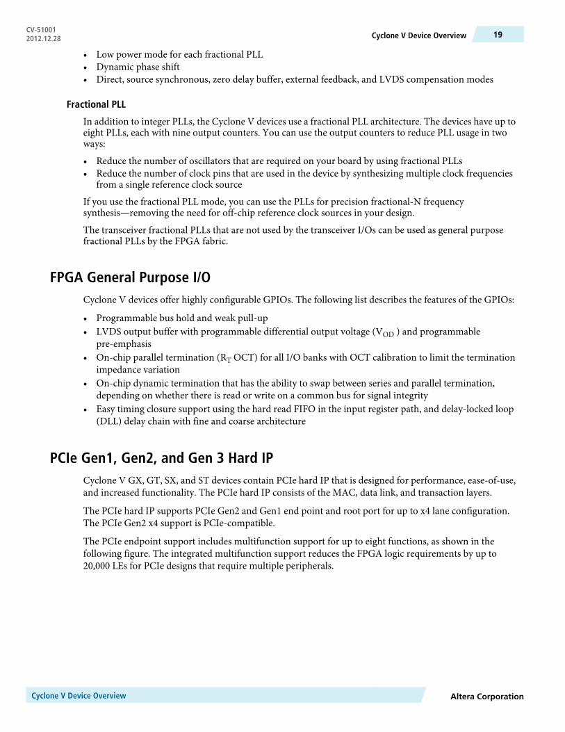
PCIe Gen1, Gen2, and Gen 3 Hard IPCyclone V GX, GT, SX, and ST devices contain PCIe hard IP that is designed for performance, ease-of-use,and increased functionality. The PCIe hard IP consists of the MAC, data link, and transaction layers.
The PCIe hard IP supports PCIe Gen2 and Gen1 end point and root port for up to x4 lane configuration.The PCIe Gen2 x4 support is PCIe-compatible.
The PCIe endpoint support includes multifunction support for up to eight functions, as shown in thefollowing figure. The integrated multifunction support reduces the FPGA logic requirements by up to20,000 LEs for PCIe designs that require multiple peripherals.
Altera CorporationCyclone V Device Overview
19Cyclone V Device OverviewCV-510012012.12.28
Figure 9: PCIe Multifunction for Cyclone V Devices
PCIe Link
External System FPGA Device
Host CPU
Memo
ryCo
ntroller
RootComplex
LocalPeripheral 1
LocalPeripheral 2
PCIeRP
PCIeEP
CAN
GbE
ATA
Bridg
etoPC
Ie
SPI
GPIO
I2 C USB
The Cyclone V PCIe hard IP operates independently from the core logic. This independent operation allowsthe PCIe link to wake up and complete link training in less than 100mswhile the CycloneV device completesloading the programming file for the rest of the device.
In addition, the PCIe hard IP in the Cyclone V device provides improved end-to-end datapath protectionusing ECC.
External Memory InterfaceThis section provides an overview of the external memory interface in Cyclone V devices.
Hard and Soft Memory ControllersCyclone V devices support up to two hard memory controllers for DDR3, DDR2, and LPDDR2 SDRAMdevices. Each controller supports 8 to 32 bit components of up to 4 gigabits (Gb) in density with two chipselects and optional ECC. For the Cyclone V SoC FPGA devices, an additional hard memory controller inthe HPS supports DDR3, DDR2, and LPDDR2 SDRAM devices.
All Cyclone V devices support soft memory controllers for DDR3, DDR2, and LPDDR2 SDRAM devicesfor maximum flexibility.
External Memory Performance
Table 20: External Memory Interface Performance in Cyclone V Devices
Soft Controller (MHz)Hard Controller (MHz)Voltage (V)Interface
3004001.5DDR3 SDRAM
3004001.35
3004001.8DDR2 SDRAM
3003331.2LPDDR2 SDRAM
Cyclone V Device OverviewAltera Corporation
CV-51001Cyclone V Device Overview20 2012.12.28
HPS External Memory Performance
Table 21: HPS External Memory Interface Performance
The hard processor system (HPS) is available in Cyclone V SoC FPGA devices only.HPS Hard Controller (MHz)Voltage (V)Interface
4001.5DDR3 SDRAM
4001.35
4001.8DDR2 SDRAM
4001.5
3331.2LPDDR2 SDRAM
Low-Power Serial TransceiversCyclone V devices deliver the industry’s lowest power 5 Gbps transceivers at an estimated 88 mW maximumpower consumption per channel. Cyclone V transceivers are designed to be compliant with a wide range ofprotocols and data rates.
Transceiver ChannelsThe transceivers are positioned on the left outer edge of the device. The transceiver channels consist of thephysical medium attachment (PMA), physical coding sublayer (PCS), and clock networks.
Altera CorporationCyclone V Device Overview
21Cyclone V Device OverviewCV-510012012.12.28
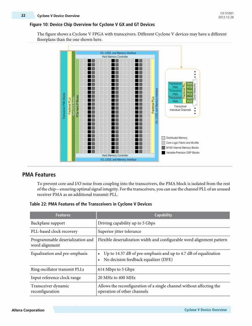
Figure 10: Device Chip Overview for Cyclone V GX and GT Devices
The figure shows a Cyclone V FPGA with transceivers. Different Cyclone V devices may have a differentfloorplans than the one shown here.
I/O, LVDS, and Memory Interface
I/O, LVDS, and Memory Interface
I/O,LVD
S,andM
emoryInte
rface
Transceiv
erPM
ABlocks
FractionalPLLs
HardPC
SBlocks FractionalPLL
FractionalPLLs
PCIeHa
rdIP
Blocks
Hard Memory Controller
Hard Memory Controller
Core Logic Fabric and MLABs
Variable-Precision DSP BlocksM10K Internal Memory Blocks
Distributed Memory
TransceiverPMA
TransceiverPMA
TransceiverPMA
HardPCS
HardPCS
HardPCS
ClockN
etworks
TransceiverIndividual Channels
PMA FeaturesTo prevent core and I/O noise from coupling into the transceivers, the PMA block is isolated from the restof the chip—ensuring optimal signal integrity. For the transceivers, you can use the channel PLL of an unusedreceiver PMA as an additional transmit PLL.
Table 22: PMA Features of the Transceivers in Cyclone V Devices
CapabilityFeatures
Driving capability up to 5 GbpsBackplane support
Superior jitter tolerancePLL-based clock recovery
Flexible deserialization width and configurable word alignment patternProgrammable deserialization andword alignment
• Up to 14.37 dB of pre-emphasis and up to 4.7 dB of equalization• No decision feedback equalizer (DFE)
Equalization and pre-emphasis
614 Mbps to 5 GbpsRing oscillator transmit PLLs
20 MHz to 400 MHzInput reference clock range
Allows the reconfiguration of a single channel without affecting theoperation of other channels
Transceiver dynamicreconfiguration
Cyclone V Device OverviewAltera Corporation
CV-51001Cyclone V Device Overview22 2012.12.28
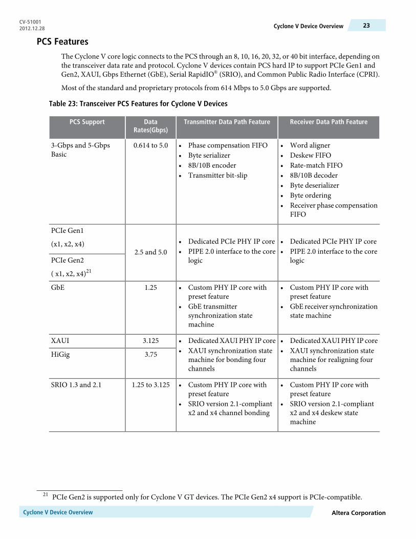
PCS FeaturesThe Cyclone V core logic connects to the PCS through an 8, 10, 16, 20, 32, or 40 bit interface, depending onthe transceiver data rate and protocol. Cyclone V devices contain PCS hard IP to support PCIe Gen1 andGen2, XAUI, Gbps Ethernet (GbE), Serial RapidIO® (SRIO), and Common Public Radio Interface (CPRI).
Most of the standard and proprietary protocols from 614 Mbps to 5.0 Gbps are supported.
Table 23: Transceiver PCS Features for Cyclone V Devices
Receiver Data Path FeatureTransmitter Data Path FeatureDataRates(Gbps)
PCS Support
• Word aligner• Deskew FIFO• Rate-match FIFO• 8B/10B decoder• Byte deserializer• Byte ordering• Receiver phase compensation
FIFO
• Phase compensation FIFO• Byte serializer• 8B/10B encoder• Transmitter bit-slip
0.614 to 5.03-Gbps and 5-GbpsBasic
• Dedicated PCIe PHY IP core• PIPE 2.0 interface to the core
logic
• Dedicated PCIe PHY IP core• PIPE 2.0 interface to the core
logic2.5 and 5.0
PCIe Gen1
(x1, x2, x4)
PCIe Gen2
( x1, x2, x4)21
• Custom PHY IP core withpreset feature
• GbE receiver synchronizationstate machine
• Custom PHY IP core withpreset feature
• GbE transmittersynchronization statemachine
1.25GbE
• DedicatedXAUIPHY IP core• XAUI synchronization state
machine for realigning fourchannels
• DedicatedXAUIPHY IP core• XAUI synchronization state
machine for bonding fourchannels
3.125XAUI
3.75HiGig
• Custom PHY IP core withpreset feature
• SRIO version 2.1-compliantx2 and x4 deskew statemachine
• Custom PHY IP core withpreset feature
• SRIO version 2.1-compliantx2 and x4 channel bonding
1.25 to 3.125SRIO 1.3 and 2.1
21 PCIe Gen2 is supported only for Cyclone V GT devices. The PCIe Gen2 x4 support is PCIe-compatible.
Altera CorporationCyclone V Device Overview
23Cyclone V Device OverviewCV-510012012.12.28
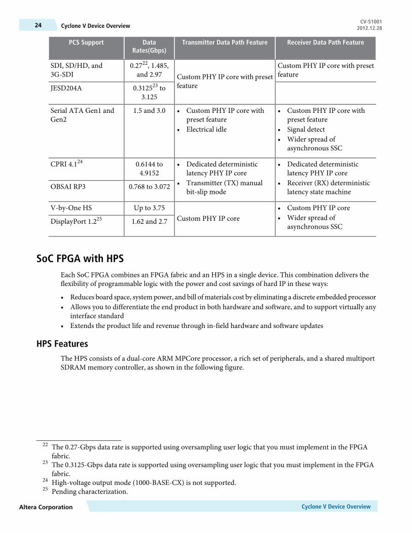
Receiver Data Path FeatureTransmitter Data Path FeatureDataRates(Gbps)
PCS Support
Custom PHY IP core with presetfeatureCustom PHY IP core with preset
feature
0.2722, 1.485,and 2.97
SDI, SD/HD, and3G-SDI
0.312523 to3.125
JESD204A
• Custom PHY IP core withpreset feature
• Signal detect• Wider spread of
asynchronous SSC
• Custom PHY IP core withpreset feature
• Electrical idle
1.5 and 3.0Serial ATA Gen1 andGen2
• Dedicated deterministiclatency PHY IP core
• Receiver (RX) deterministiclatency state machine
• Dedicated deterministiclatency PHY IP core
• Transmitter (TX) manualbit-slip mode
0.6144 to4.9152
CPRI 4.124
0.768 to 3.072OBSAI RP3
• Custom PHY IP core• Wider spread of
asynchronous SSCCustom PHY IP core
Up to 3.75V-by-One HS
1.62 and 2.7DisplayPort 1.225
SoC FPGA with HPSEach SoC FPGA combines an FPGA fabric and an HPS in a single device. This combination delivers theflexibility of programmable logic with the power and cost savings of hard IP in these ways:
• Reduces board space, systempower, and bill ofmaterials cost by eliminating a discrete embedded processor• Allows you to differentiate the end product in both hardware and software, and to support virtually any
interface standard• Extends the product life and revenue through in-field hardware and software updates
HPS FeaturesThe HPS consists of a dual-core ARM MPCore processor, a rich set of peripherals, and a shared multiportSDRAM memory controller, as shown in the following figure.
22 The 0.27-Gbps data rate is supported using oversampling user logic that you must implement in the FPGAfabric.
23 The 0.3125-Gbps data rate is supported using oversampling user logic that you must implement in the FPGAfabric.
24 High-voltage output mode (1000-BASE-CX) is not supported.25 Pending characterization.
Cyclone V Device OverviewAltera Corporation
CV-51001Cyclone V Device Overview24 2012.12.28
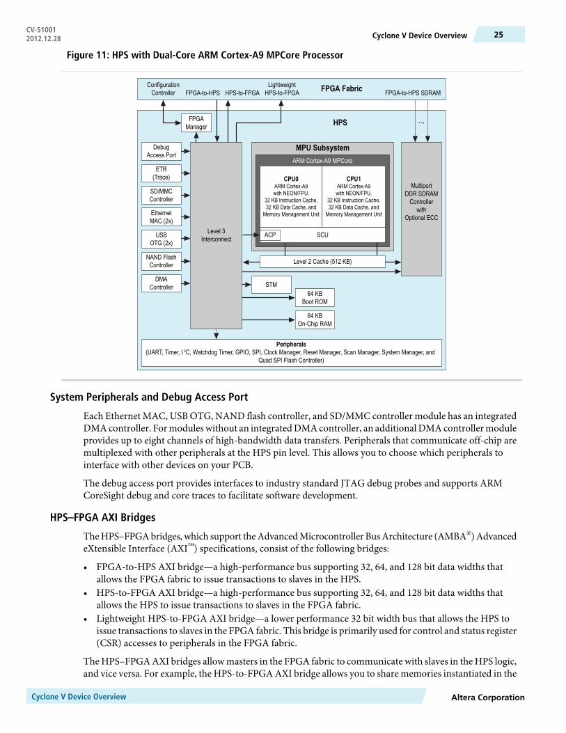
Figure 11: HPS with Dual-Core ARM Cortex-A9 MPCore Processor
FPGA Fabric
HPS
HPS-to-FPGALightweight
HPS-to-FPGAFPGA-to-HPS FPGA-to-HPS SDRAMConfigurationController
FPGAManager
64 KBOn-Chip RAM
64 KBBoot ROM
Level 3Interconnect
EthernetMAC (2x)
USBOTG (2x)
NAND FlashController
SD/MMCController
DMAController STM
ETR(Trace)
DebugAccess Port
ARM Cortex-A9 MPCore
MPU Subsystem
CPU0ARM Cortex-A9with NEON/FPU,
32 KB Instruction Cache,32 KB Data Cache, and
Memory Management Unit
CPU1ARM Cortex-A9with NEON/FPU,
32 KB Instruction Cache,32 KB Data Cache, and
Memory Management Unit
SCUACP
Level 2 Cache (512 KB)
MultiportDDR SDRAMController
withOptional ECC
Peripherals(UART, Timer, I 2C, Watchdog Timer, GPIO, SPI, Clock Manager, Reset Manager, Scan Manager, System Manager, and
Quad SPI Flash Controller)
System Peripherals and Debug Access Port
Each Ethernet MAC, USB OTG, NAND flash controller, and SD/MMC controller module has an integratedDMAcontroller. Formoduleswithout an integratedDMAcontroller, an additionalDMAcontrollermoduleprovides up to eight channels of high-bandwidth data transfers. Peripherals that communicate off-chip aremultiplexed with other peripherals at the HPS pin level. This allows you to choose which peripherals tointerface with other devices on your PCB.
The debug access port provides interfaces to industry standard JTAG debug probes and supports ARMCoreSight debug and core traces to facilitate software development.
HPS–FPGA AXI Bridges
TheHPS–FPGAbridges, which support theAdvancedMicrocontroller BusArchitecture (AMBA®)AdvancedeXtensible Interface (AXI™) specifications, consist of the following bridges:
• FPGA-to-HPS AXI bridge—a high-performance bus supporting 32, 64, and 128 bit data widths thatallows the FPGA fabric to issue transactions to slaves in the HPS.
• HPS-to-FPGA AXI bridge—a high-performance bus supporting 32, 64, and 128 bit data widths thatallows the HPS to issue transactions to slaves in the FPGA fabric.
• Lightweight HPS-to-FPGA AXI bridge—a lower performance 32 bit width bus that allows the HPS toissue transactions to slaves in the FPGA fabric. This bridge is primarily used for control and status register(CSR) accesses to peripherals in the FPGA fabric.
The HPS–FPGA AXI bridges allow masters in the FPGA fabric to communicate with slaves in the HPS logic,and vice versa. For example, the HPS-to-FPGA AXI bridge allows you to share memories instantiated in the
Altera CorporationCyclone V Device Overview
25Cyclone V Device OverviewCV-510012012.12.28
FPGA fabric with one or both microprocessors in the HPS, while the FPGA-to-HPS AXI bridge allows logicin the FPGA fabric to access the memory and peripherals in the HPS.
Each HPS–FPGA bridge also provides asynchronous clock crossing for data transferred between the FPGAfabric and the HPS.
HPS SDRAM Controller Subsystem
The HPS SDRAM controller subsystem contains a multiport SDRAM controller and DDR PHY that areshared between the FPGA fabric (through the FPGA-to-HPS SDRAM interface), the level 2 (L2) cache, andthe level 3 (L3) system interconnect. The FPGA-to-HPS SDRAM interface supports AMBAAXI andAvalon®
Memory-Mapped (Avalon-MM) interface standards, and provides up to six individual ports for access bymasters implemented in the FPGA fabric.
To maximize memory performance, the SDRAM controller subsystem supports command and datareordering, deficit round-robin arbitration with aging, and high-priority bypass features. The SDRAMcontroller subsystem supports DDR2, DDR3, or LPDDR2 devices up to 4 Gb in density operating at up to400 MHz (800 Mbps data rate).
FPGA Configuration and Processor BootingThe FPGA fabric andHPS in the SoCFPGAare powered independently. You can reduce the clock frequenciesor gate the clocks to reduce dynamic power, or shut down the entire FPGA fabric to reduce total systempower.
You can configure the FPGA fabric and boot the HPS independently, in any order, providing you with moredesign flexibility:
• You can boot theHPS independently. After theHPS is running, theHPS can fully or partially reconfigurethe FPGA fabric at any time under software control. The HPS can also configure other FPGAs on theboard through the FPGA configuration controller.
• You can power up both the HPS and the FPGA fabric together, configure the FPGA fabric first, and thenboot the HPS from memory accessible to the FPGA fabric.
Although the FPGA fabric and HPS are on separate power domains, the HPS must remain poweredup during operation while the FPGA fabric can be powered up or down as required.
Note:
Hardware and Software DevelopmentFor hardware development, you can configure the HPS and connect your soft logic in the FPGA fabric tothe HPS interfaces using the Qsys system integration tool in the Quartus II software.
For software development, the ARM-based SoC FPGA devices inherit the rich software developmentecosystem available for the ARM Cortex-A9 MPCore processor. The software development process forAltera SoC FPGAs follows the same steps as those for other SoC devices from other manufacturers. Supportfor Linux, VxWorks®, and other operating systemswill be available for the SoCFPGAs. Formore informationon the operating systems support availability, contact the Altera sales team.
You can begin device-specific firmware and software development on the Altera SoC FPGA Virtual Target.The Virtual Target is a fast PC-based functional simulation of a target development system—a model of acomplete development board that runs on a PC. TheVirtual Target enables the development of device-specificproduction software that can run unmodified on actual hardware.
Cyclone V Device OverviewAltera Corporation
CV-51001Cyclone V Device Overview26 2012.12.28
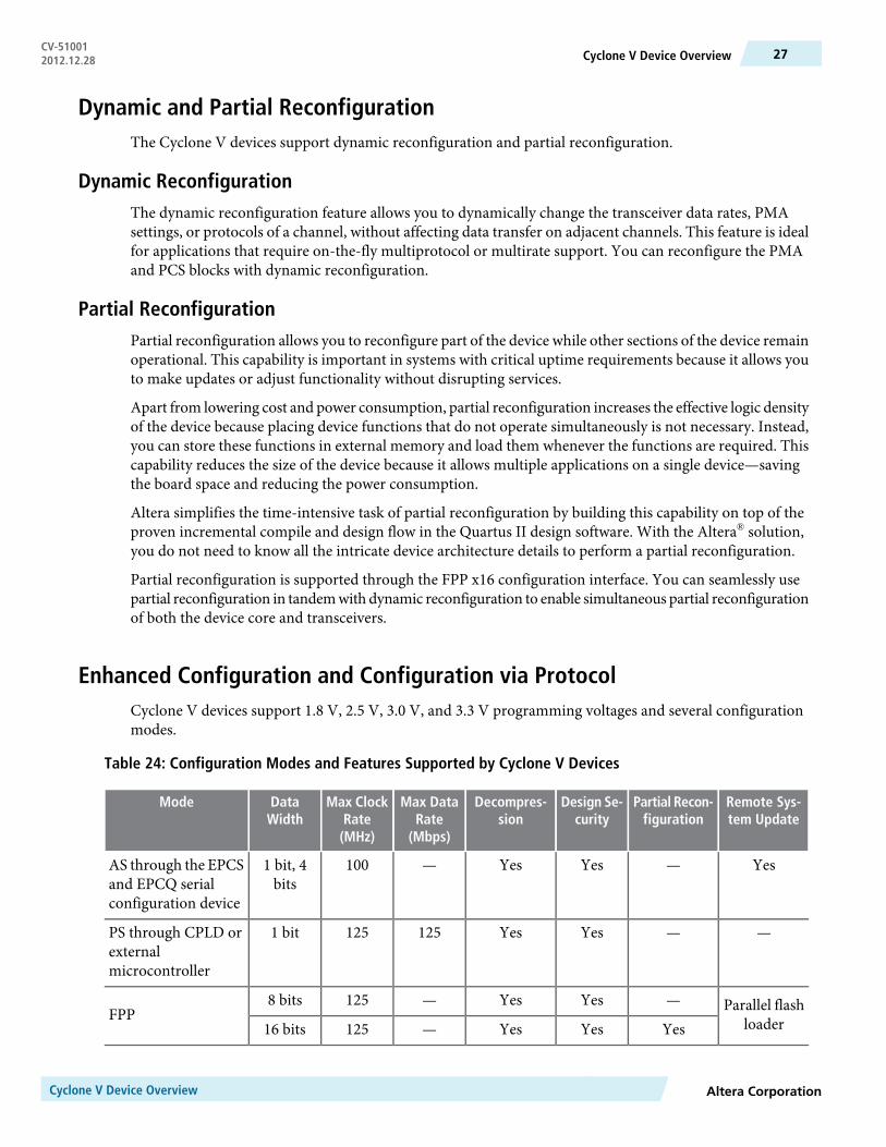
Dynamic and Partial ReconfigurationThe Cyclone V devices support dynamic reconfiguration and partial reconfiguration.
Dynamic ReconfigurationThe dynamic reconfiguration feature allows you to dynamically change the transceiver data rates, PMAsettings, or protocols of a channel, without affecting data transfer on adjacent channels. This feature is idealfor applications that require on-the-fly multiprotocol or multirate support. You can reconfigure the PMAand PCS blocks with dynamic reconfiguration.
Partial ReconfigurationPartial reconfiguration allows you to reconfigure part of the device while other sections of the device remainoperational. This capability is important in systems with critical uptime requirements because it allows youto make updates or adjust functionality without disrupting services.
Apart from lowering cost and power consumption, partial reconfiguration increases the effective logic densityof the device because placing device functions that do not operate simultaneously is not necessary. Instead,you can store these functions in external memory and load them whenever the functions are required. Thiscapability reduces the size of the device because it allows multiple applications on a single device—savingthe board space and reducing the power consumption.
Altera simplifies the time-intensive task of partial reconfiguration by building this capability on top of theproven incremental compile and design flow in the Quartus II design software. With the Altera® solution,you do not need to know all the intricate device architecture details to perform a partial reconfiguration.
Partial reconfiguration is supported through the FPP x16 configuration interface. You can seamlessly usepartial reconfiguration in tandemwith dynamic reconfiguration to enable simultaneous partial reconfigurationof both the device core and transceivers.
Enhanced Configuration and Configuration via ProtocolCyclone V devices support 1.8 V, 2.5 V, 3.0 V, and 3.3 V programming voltages and several configurationmodes.
Table 24: Configuration Modes and Features Supported by Cyclone V Devices
Remote Sys-tem Update
Partial Recon-figuration
Design Se-curity
Decompres-sion
Max DataRate
(Mbps)
Max ClockRate(MHz)
DataWidth
Mode
Yes—YesYes—1001 bit, 4bits
AS through the EPCSand EPCQ serialconfiguration device
——YesYes1251251 bitPS through CPLD orexternalmicrocontroller
Parallel flashloader
—YesYes—1258 bitsFPP
YesYesYes—12516 bits
Altera CorporationCyclone V Device Overview
27Cyclone V Device OverviewCV-510012012.12.28
Remote Sys-tem Update
Partial Recon-figuration
Design Se-curity
Decompres-sion
Max DataRate
(Mbps)
Max ClockRate(MHz)
DataWidth
Mode
——Yes———x1, x2,and x4lanes
CvP (PCIe)
————33331 bitJTAG
Instead of using an external flash or ROM, you can configure the Cyclone V devices through PCIe usingCvP. The CvP mode offers the fastest configuration rate and flexibility with the easy-to-use PCIe hard IPblock interface. The Cyclone V CvP implementation conforms to the PCIe 100 ms power-up-to-active timerequirement.
For more information about CvP, refer to the Configuration via Protocol (CvP) Implementation in AlteraFPGAs User Guide.
Power ManagementLeveraging the FPGA architectural features, process technology advancements, and transceivers that aredesigned for power efficiency, the Cyclone V devices consume less power than previous generation CycloneFPGAs:
• Total device core power consumption—less by up to 40%.• Transceiver channel power consumption—less by up to 50%.
Additionally, Cyclone V devices contain several hard IP blocks that reduce logic resources and deliversubstantial power savings of up to 25% less power than equivalent soft implementations.
Document Revision History
ChangesVersionDate
• Updated the pin counts for the MBGA packages.• Updated the GPIO and transceiver counts for the MBGA packages.• Updated the GPIO counts for the U484 package of the Cyclone V E
A9, GX C9, and GT D9 devices.• Updated the vertical migration table for vertical migration of the U484
packages.• Updated the MLAB supported programmable widths at 32 bits depth.
2012.12.28December 2012
Cyclone V Device OverviewAltera Corporation
CV-51001Cyclone V Device Overview28 2012.12.28
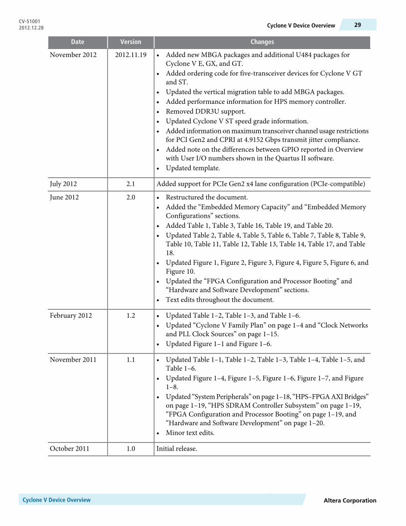
ChangesVersionDate
• Added new MBGA packages and additional U484 packages forCyclone V E, GX, and GT.
• Added ordering code for five-transceiver devices for Cyclone V GTand ST.
• Updated the vertical migration table to add MBGA packages.• Added performance information for HPS memory controller.• Removed DDR3U support.• Updated Cyclone V ST speed grade information.• Added information onmaximum transceiver channel usage restrictions
for PCI Gen2 and CPRI at 4.9152 Gbps transmit jitter compliance.• Added note on the differences between GPIO reported in Overview
with User I/O numbers shown in the Quartus II software.• Updated template.
2012.11.19November 2012
Added support for PCIe Gen2 x4 lane configuration (PCIe-compatible)2.1July 2012
• Restructured the document.• Added the “Embedded Memory Capacity” and “Embedded Memory
Configurations” sections.• Added Table 1, Table 3, Table 16, Table 19, and Table 20.• Updated Table 2, Table 4, Table 5, Table 6, Table 7, Table 8, Table 9,
Table 10, Table 11, Table 12, Table 13, Table 14, Table 17, and Table18.
• Updated Figure 1, Figure 2, Figure 3, Figure 4, Figure 5, Figure 6, andFigure 10.
• Updated the “FPGA Configuration and Processor Booting” and“Hardware and Software Development” sections.
• Text edits throughout the document.
2.0June 2012
• Updated Table 1–2, Table 1–3, and Table 1–6.• Updated “Cyclone V Family Plan” on page 1–4 and “Clock Networks
and PLL Clock Sources” on page 1–15.• Updated Figure 1–1 and Figure 1–6.
1.2February 2012
• Updated Table 1–1, Table 1–2, Table 1–3, Table 1–4, Table 1–5, andTable 1–6.
• Updated Figure 1–4, Figure 1–5, Figure 1–6, Figure 1–7, and Figure1–8.
• Updated “SystemPeripherals”onpage 1–18, “HPS–FPGAAXIBridges”on page 1–19, “HPS SDRAM Controller Subsystem” on page 1–19,“FPGA Configuration and Processor Booting” on page 1–19, and“Hardware and Software Development” on page 1–20.
• Minor text edits.
1.1November 2011
Initial release.1.0October 2011
Altera CorporationCyclone V Device Overview
29Cyclone V Device OverviewCV-510012012.12.28