Cyclone II Device Family Data Sheet, Cyclone II Device...
138
Altera Corporation Section I–1 Preliminary Section I. Cyclone II Device Family Data Sheet This section provides information for board layout designers to successfully layout their boards for Cyclone ™ II devices. It contains the required PCB layout guidelines, device pin tables, and package specifications. This section includes the following chapters: ■ Chapter 1. Introduction ■ Chapter 2. Cyclone II Architecture ■ Chapter 3. Configuration & Testing ■ Chapter 4. Hot Socketing & Power-On Reset ■ Chapter 5. DC Characteristics & Timing Specifications ■ Chapter 6. Reference & Ordering Information
Transcript of Cyclone II Device Family Data Sheet, Cyclone II Device...
Altera Corporation
Section I. Cyclone IIDevice Family Data Sheet
This section provides information for board layout designers to successfully layout their boards for Cyclone™ II devices. It contains the required PCB layout guidelines, device pin tables, and package specifications.
This section includes the following chapters:
■ Chapter 1. Introduction
■ Chapter 2. Cyclone II Architecture
■ Chapter 3. Configuration & Testing
■ Chapter 4. Hot Socketing & Power-On Reset
■ Chapter 5. DC Characteristics & Timing Specifications
■ Chapter 6. Reference & Ordering Information
Section I–1Preliminary
Cyclone II Device Family Data Sheet Cyclone II Device Handbook, Volume 1
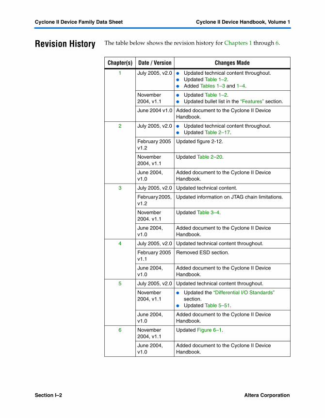
Revision History The table below shows the revision history for Chapters 1 through 6.
Chapter(s) Date / Version Changes Made
1 July 2005, v2.0 ● Updated technical content throughout.● Updated Table 1–2.● Added Tables 1–3 and 1–4.
November 2004, v1.1
● Updated Table 1–2.● Updated bullet list in the “Features” section.
June 2004 v1.0 Added document to the Cyclone II Device Handbook.
2 July 2005, v2.0 ● Updated technical content throughout.● Updated Table 2–17.
February 2005 v1.2
Updated figure 2-12.
November 2004, v1.1
Updated Table 2–20.
June 2004, v1.0
Added document to the Cyclone II Device Handbook.
3 July 2005, v2.0 Updated technical content.
February 2005, v1.2
Updated information on JTAG chain limitations.
November 2004. v1.1
Updated Table 3–4.
June 2004, v1.0
Added document to the Cyclone II Device Handbook.
4 July 2005, v2.0 Updated technical content throughout.
February 2005 v1.1
Removed ESD section.
June 2004, v1.0
Added document to the Cyclone II Device Handbook.
5 July 2005, v2.0 Updated technical content throughout.
November 2004, v1.1
● Updated the “Differential I/O Standards” section.
● Updated Table 5–51.
June 2004, v1.0
Added document to the Cyclone II Device Handbook.
6 November 2004, v1.1
Updated Figure 6–1.
June 2004, v1.0
Added document to the Cyclone II Device Handbook.
Section I–2 Altera CorporationPreliminary
Altera Corporation July 2005
CII51001-2.0
1. Introduction
Introduction Altera’s low-cost CycloneTM II FPGA family is based on a 1.2-V, 90-nm SRAM process with densities over 68K logic elements (LEs) and up to 1.1 Mbits of embedded RAM. With features like embedded 18 × 18 multipliers to support high-performance DSP applications, phase-locked loops (PLLs) for system clock management, and high-speed external memory interface support for SRAM and DRAM devices, Cyclone II devices are a cost-effective solution for high-volume applications. Cyclone II devices support differential and single-ended I/O standards, including LVDS at data rates up to 805 megabits per second (Mbps) for the receiver and 640 Mbps for the transmitter, and 64-bit, 66-MHz PCI and PCI-X for interfacing with processors and ASSP and ASIC devices. Altera also offers low-cost serial configuration devices to configure Cyclone II devices. The Cyclone II FPGA family offers commercial grade, industrial grade, and lead-free devices.
Features The Cyclone II device family offers the following features:
■ High-density architecture with 4,608 to 68,416 LEs■ M4K embedded memory blocks
● Up to 1.1 Mbits of RAM available without reducing available logic
● 4,096 memory bits per block (4,608 bits per block including 512 parity bits)
● Variable port configurations of ×1, ×2, ×4, ×8, ×9, ×16, ×18, ×32, and ×36
● True dual-port (one read and one write, two reads, or two writes) operation for ×1, ×2, ×4, ×8, ×9, ×16, and ×18 modes
● Byte enables for data input masking during writes● Up to 260-MHz operation
■ Embedded multipliers● 18- × 18-bit multipliers are each configurable as two
independent 9- × 9-bit multipliers with up to 250-MHz performance
● Optional input and output registers■ Advanced I/O support
● High-speed differential I/O standard support, including LVDS, RSDS, mini-LVDS, LVPECL, differential HSTL, and differential SSTL
● Single-ended I/O standard support, including 2.5-V and 1.8-V SSTL class I and II, 1.8-V and 1.5-V HSTL class I and II, 3.3-V PCI
1–1Preliminary
Features
and PCI-X 1.0, 3.3-, 2.5-, 1.8-, and 1.5-V LVCMOS, and 3.3-, 2.5-, and 1.8-V LVTTL
● Peripheral component interconnect Special Interest Group (PCI SIG) PCI Local Bus Specification, Revision 3.0 compliance for 3.3-V operation at 33 or 66 MHz for 32- or 64-bit interfaces
● 133-MHz PCI-X 1.0 specification compatibility● High-speed external memory support, including DDR, DDR2,
and SDR SDRAM, and QDRII SRAM● Three dedicated registers per I/O element (IOE): one input
register, one output register, and one output-enable register● Programmable bus-hold feature● Programmable output drive strength feature● Programmable delays from the pin to the IOE or logic array● I/O bank grouping for unique VCCIO and/or VREF bank settings● MultiVoltTM I/O standard support for 1.5-, 1.8-, 2.5-, and 3.3-V
interfaces● Hot-socketing operation support● Tri-state with weak pull-up on I/O pins before and during
configuration● Programmable open-drain outputs● Series on-chip termination support
■ Flexible clock management circuitry● Hierarchical clock network for up to 402.5-MHz performance● Up to four PLLs per device provide clock multiplication and
division, phase shifting, programmable duty cycle, and external clock outputs, allowing system-level clock management and skew control
● Up to 16 global clock lines in the global clock network that drive throughout the entire device
■ Device configuration● Fast serial configuration allows configuration times less than
100 ms● Decompression feature allows for smaller programming file
storage and faster configuration times● Supports multiple configuration modes: active serial, passive
serial, and JTAG-based configuration● Supports configuration through low-cost serial configuration
devices● Device configuration supports multiple voltages (either 3.3, 2.5,
or 1.8 V)■ Intellectual property
● Altera megafunction support● Altera MegaCore® function support● Altera Megafunctions Partners Program (AMPPSM)
megafunctions support
1–2 Altera CorporationCyclone II Device Handbook, Volume 1 July 2005
Introduction
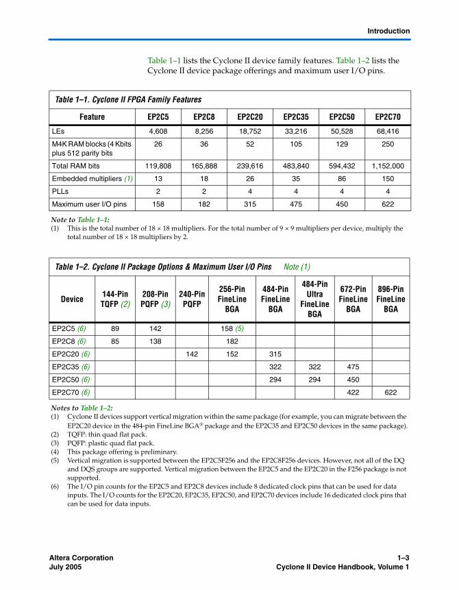
Table 1–1 lists the Cyclone II device family features. Table 1–2 lists the Cyclone II device package offerings and maximum user I/O pins.
Table 1–1. Cyclone II FPGA Family Features
Feature EP2C5 EP2C8 EP2C20 EP2C35 EP2C50 EP2C70
LEs 4,608 8,256 18,752 33,216 50,528 68,416
M4K RAM blocks (4 Kbits plus 512 parity bits
26 36 52 105 129 250
Total RAM bits 119,808 165,888 239,616 483,840 594,432 1,152,000
Embedded multipliers (1) 13 18 26 35 86 150
PLLs 2 2 4 4 4 4
Maximum user I/O pins 158 182 315 475 450 622
Note to Table 1–1:(1) This is the total number of 18 × 18 multipliers. For the total number of 9 × 9 multipliers per device, multiply the
total number of 18 × 18 multipliers by 2.
Table 1–2. Cyclone II Package Options & Maximum User I/O Pins Note (1)
Device 144-Pin TQFP (2)
208-Pin PQFP (3)
240-Pin PQFP
256-Pin FineLine
BGA
484-Pin FineLine
BGA
484-Pin Ultra
FineLine BGA
672-Pin FineLine
BGA
896-Pin FineLine
BGA
EP2C5 (6) 89 142 158 (5)
EP2C8 (6) 85 138 182
EP2C20 (6) 142 152 315
EP2C35 (6) 322 322 475
EP2C50 (6) 294 294 450
EP2C70 (6) 422 622
Notes to Table 1–2:(1) Cyclone II devices support vertical migration within the same package (for example, you can migrate between the
EP2C20 device in the 484-pin FineLine BGA® package and the EP2C35 and EP2C50 devices in the same package).(2) TQFP: thin quad flat pack.(3) PQFP: plastic quad flat pack.(4) This package offering is preliminary.(5) Vertical migration is supported between the EP2C5F256 and the EP2C8F256 devices. However, not all of the DQ
and DQS groups are supported. Vertical migration between the EP2C5 and the EP2C20 in the F256 package is not supported.
(6) The I/O pin counts for the EP2C5 and EP2C8 devices include 8 dedicated clock pins that can be used for data inputs. The I/O counts for the EP2C20, EP2C35, EP2C50, and EP2C70 devices include 16 dedicated clock pins that can be used for data inputs.
Altera Corporation 1–3July 2005 Cyclone II Device Handbook, Volume 1
Features
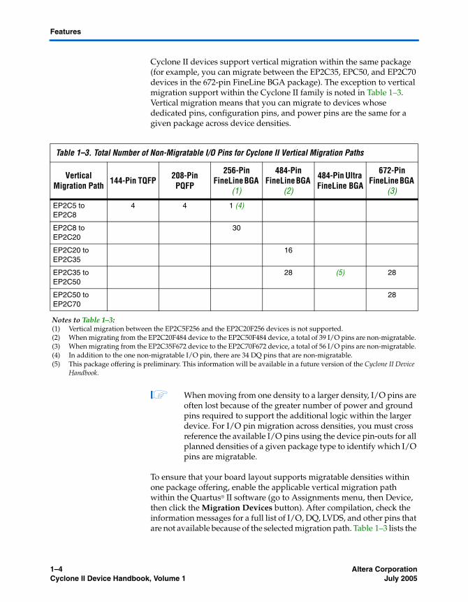
Cyclone II devices support vertical migration within the same package (for example, you can migrate between the EP2C35, EPC50, and EP2C70 devices in the 672-pin FineLine BGA package). The exception to vertical migration support within the Cyclone II family is noted in Table 1–3. Vertical migration means that you can migrate to devices whose dedicated pins, configuration pins, and power pins are the same for a given package across device densities.
1 When moving from one density to a larger density, I/O pins are often lost because of the greater number of power and ground pins required to support the additional logic within the larger device. For I/O pin migration across densities, you must cross reference the available I/O pins using the device pin-outs for all planned densities of a given package type to identify which I/O pins are migratable.
To ensure that your board layout supports migratable densities within one package offering, enable the applicable vertical migration path within the Quartus® II software (go to Assignments menu, then Device, then click the Migration Devices button). After compilation, check the information messages for a full list of I/O, DQ, LVDS, and other pins that are not available because of the selected migration path. Table 1–3 lists the
Table 1–3. Total Number of Non-Migratable I/O Pins for Cyclone II Vertical Migration Paths
Vertical Migration Path 144-Pin TQFP 208-Pin
PQFP
256-Pin FineLine BGA
(1)
484-Pin FineLine BGA
(2)
484-Pin Ultra FineLine BGA
672-Pin FineLine BGA
(3)
EP2C5 to EP2C8
4 4 1 (4)
EP2C8 to EP2C20
30
EP2C20 to EP2C35
16
EP2C35 to EP2C50
28 (5) 28
EP2C50 to EP2C70
28
Notes to Table 1–3:(1) Vertical migration between the EP2C5F256 and the EP2C20F256 devices is not supported.(2) When migrating from the EP2C20F484 device to the EP2C50F484 device, a total of 39 I/O pins are non-migratable.(3) When migrating from the EP2C35F672 device to the EP2C70F672 device, a total of 56 I/O pins are non-migratable.(4) In addition to the one non-migratable I/O pin, there are 34 DQ pins that are non-migratable.(5) This package offering is preliminary. This information will be available in a future version of the Cyclone II Device
Handbook.
1–4 Altera CorporationCyclone II Device Handbook, Volume 1 July 2005
Introduction
Cyclone II device package offerings and shows the total number of non-migratable I/O pins when migrating from one density device to a larger density device.
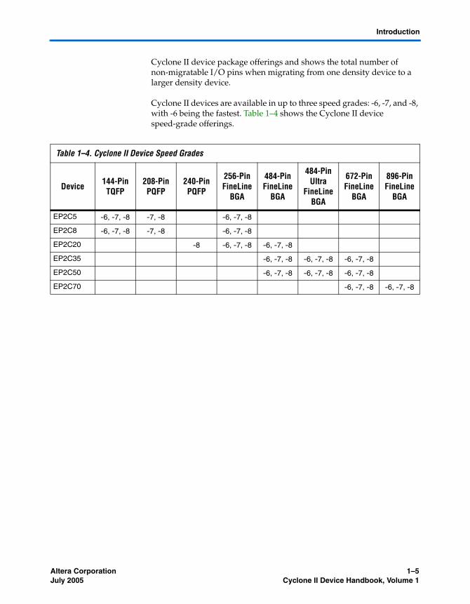
Cyclone II devices are available in up to three speed grades: -6, -7, and -8, with -6 being the fastest. Table 1–4 shows the Cyclone II device speed-grade offerings.
Table 1–4. Cyclone II Device Speed Grades
Device 144-Pin TQFP
208-Pin PQFP
240-Pin PQFP
256-Pin FineLine
BGA
484-Pin FineLine
BGA
484-Pin Ultra
FineLine BGA
672-Pin FineLine
BGA
896-Pin FineLine
BGA
EP2C5 -6, -7, -8 -7, -8 -6, -7, -8
EP2C8 -6, -7, -8 -7, -8 -6, -7, -8
EP2C20 -8 -6, -7, -8 -6, -7, -8
EP2C35 -6, -7, -8 -6, -7, -8 -6, -7, -8
EP2C50 -6, -7, -8 -6, -7, -8 -6, -7, -8
EP2C70 -6, -7, -8 -6, -7, -8
Altera Corporation 1–5July 2005 Cyclone II Device Handbook, Volume 1
Features
1–6 Altera CorporationCyclone II Device Handbook, Volume 1 July 2005
Altera Corporation July 2005
CII51002-2.0
2. Cyclone II Architecture
Functional Description
Cyclone™ II devices contain a two-dimensional row- and column-based architecture to implement custom logic. Column and row interconnects of varying speeds provide signal interconnects between logic array blocks (LABs), embedded memory blocks, and embedded multipliers.
The logic array consists of LABs, with 16 logic elements (LEs) in each LAB. An LE is a small unit of logic providing efficient implementation of user logic functions. LABs are grouped into rows and columns across the device. Cyclone II devices range in density from 4,608 to 68,416 LEs.
Cyclone II devices provide a global clock network and up to four phase-locked loops (PLLs). The global clock network consists of up to 16 global clock lines that drive throughout the entire device. The global clock network can provide clocks for all resources within the device, such as input/output elements (IOEs), LEs, embedded multipliers, and embedded memory blocks. The global clock lines can also be used for other high fan-out signals. Cyclone II PLLs provide general-purpose clocking with clock synthesis and phase shifting as well as external outputs for high-speed differential I/O support.
M4K memory blocks are true dual-port memory blocks with 4K bits of memory plus parity (4,608 bits). These blocks provide dedicated true dual-port, simple dual-port, or single-port memory up to 36-bits wide at up to 260 MHz. These blocks are arranged in columns across the device in between certain LABs. Cyclone II devices offer between 119 to 1,152 Kbits of embedded memory.
Each embedded multiplier block can implement up to either two 9 × 9-bit multipliers, or one 18 × 18-bit multiplier with up to 250-MHz performance. Embedded multipliers are arranged in columns across the device.
Each Cyclone II device I/O pin is fed by an IOE located at the ends of LAB rows and columns around the periphery of the device. I/O pins support various single-ended and differential I/O standards, such as the 66- and 33-MHz, 64- and 32-bit PCI standard, PCI-X, and the LVDS I/O standard at a maximum data rate of 805 megabits per second (Mbps) for inputs and 640 Mbps for outputs. Each IOE contains a bidirectional I/O buffer and three registers for registering input, output, and output-enable signals. Dual-purpose DQS, DQ, and DM pins along with delay chains (used to
2–1Preliminary
Functional Description
phase-align double data rate (DDR) signals) provide interface support for external memory devices such as DDR, DDR2, and single data rate (SDR) SDRAM, and QDRII SRAM devices at up to 167 MHz.
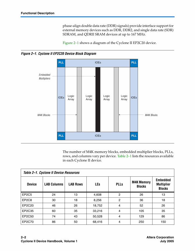
Figure 2–1 shows a diagram of the Cyclone II EP2C20 device.
Figure 2–1. Cyclone II EP2C20 Device Block Diagram
The number of M4K memory blocks, embedded multiplier blocks, PLLs, rows, and columns vary per device. Table 2–1 lists the resources available in each Cyclone II device.
PLL PLLIOEs
PLL PLLIOEs
IOEs LogicArray
LogicArray
LogicArray
LogicArray
IOEs
M4K BlocksM4K Blocks
EmbeddedMultipliers
Table 2–1. Cyclone II Device Resources
Device LAB Columns LAB Rows LEs PLLs M4K Memory Blocks
Embedded Multiplier
Blocks
EP2C5 24 13 4,608 2 26 13
EP2C8 30 18 8,256 2 36 18
EP2C20 46 26 18,752 4 52 26
EP2C35 60 35 33,216 4 105 35
EP2C50 74 43 50,528 4 129 86
EP2C70 86 50 68,416 4 250 150
2–2 Altera CorporationCyclone II Device Handbook, Volume 1 July 2005
Cyclone II Architecture
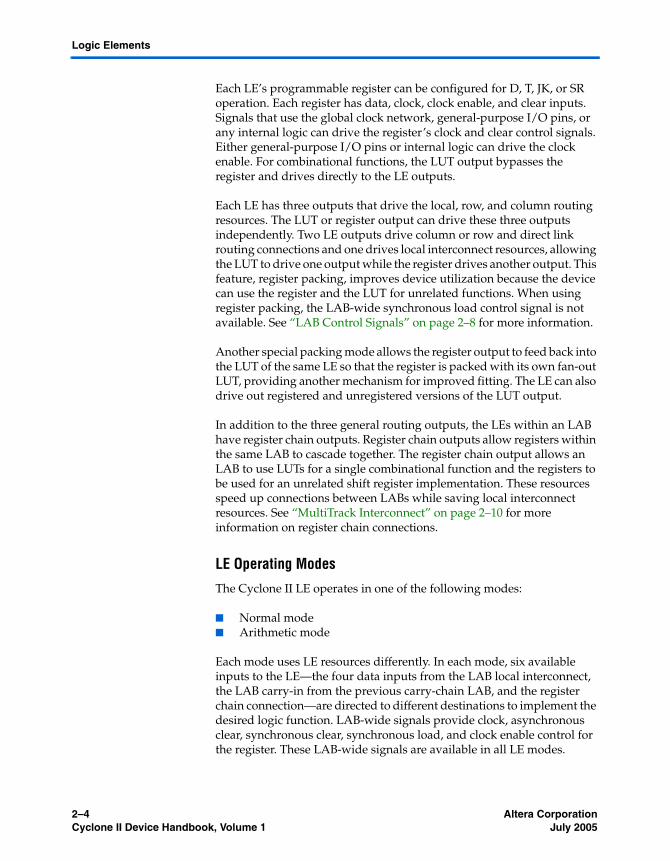
Logic Elements The smallest unit of logic in the Cyclone II architecture, the LE, is compact and provides advanced features with efficient logic utilization. Each LE features:
■ A four-input look-up table (LUT), which is a function generator that can implement any function of four variables
■ A programmable register■ A carry chain connection■ A register chain connection■ The ability to drive all types of interconnects: local, row, column,
register chain, and direct link interconnects■ Support for register packing■ Support for register feedback
Figure 2–2 shows a Cyclone II LE.
Figure 2–2. Cyclone II LE
labclk1
labclk2
labclr2
LAB Carry-In
Clock &Clock Enable
Select
LAB Carry-Out
Look-UpTable(LUT)
CarryChain
Row, Column,And Direct Link Routing
Row, Column,And Direct Link Routing
ProgrammableRegister
CLRN
D Q
ENA
Register Bypass
PackedRegister Select
Chip-WideReset
(DEV_CLRn)
labclkena1labclkena2
SynchronousLoad andClear Logic
LAB-WideSynchronous
LoadLAB-Wide
SynchronousClear
AsynchronousClear Logic
data1data2data3
data4
labclr1
Local Routing
Register ChainOutputRegister
Feedback
Register ChainRouting FromPrevious LE
Altera Corporation 2–3July 2005 Cyclone II Device Handbook, Volume 1
Logic Elements
Each LE’s programmable register can be configured for D, T, JK, or SR operation. Each register has data, clock, clock enable, and clear inputs. Signals that use the global clock network, general-purpose I/O pins, or any internal logic can drive the register’s clock and clear control signals. Either general-purpose I/O pins or internal logic can drive the clock enable. For combinational functions, the LUT output bypasses the register and drives directly to the LE outputs.
Each LE has three outputs that drive the local, row, and column routing resources. The LUT or register output can drive these three outputs independently. Two LE outputs drive column or row and direct link routing connections and one drives local interconnect resources, allowing the LUT to drive one output while the register drives another output. This feature, register packing, improves device utilization because the device can use the register and the LUT for unrelated functions. When using register packing, the LAB-wide synchronous load control signal is not available. See “LAB Control Signals” on page 2–8 for more information.
Another special packing mode allows the register output to feed back into the LUT of the same LE so that the register is packed with its own fan-out LUT, providing another mechanism for improved fitting. The LE can also drive out registered and unregistered versions of the LUT output.
In addition to the three general routing outputs, the LEs within an LAB have register chain outputs. Register chain outputs allow registers within the same LAB to cascade together. The register chain output allows an LAB to use LUTs for a single combinational function and the registers to be used for an unrelated shift register implementation. These resources speed up connections between LABs while saving local interconnect resources. See “MultiTrack Interconnect” on page 2–10 for more information on register chain connections.
LE Operating Modes
The Cyclone II LE operates in one of the following modes:
■ Normal mode■ Arithmetic mode
Each mode uses LE resources differently. In each mode, six available inputs to the LE—the four data inputs from the LAB local interconnect, the LAB carry-in from the previous carry-chain LAB, and the register chain connection—are directed to different destinations to implement the desired logic function. LAB-wide signals provide clock, asynchronous clear, synchronous clear, synchronous load, and clock enable control for the register. These LAB-wide signals are available in all LE modes.
2–4 Altera CorporationCyclone II Device Handbook, Volume 1 July 2005
Cyclone II Architecture
The Quartus® II software, in conjunction with parameterized functions such as library of parameterized modules (LPM) functions, automatically chooses the appropriate mode for common functions such as counters, adders, subtractors, and arithmetic functions. If required, you can also create special-purpose functions that specify which LE operating mode to use for optimal performance.
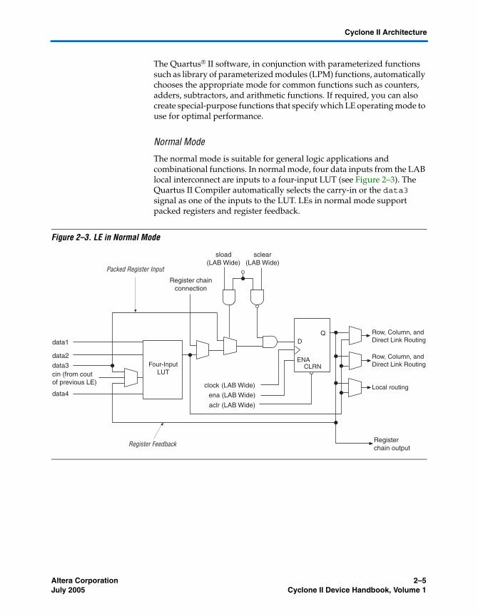
Normal Mode
The normal mode is suitable for general logic applications and combinational functions. In normal mode, four data inputs from the LAB local interconnect are inputs to a four-input LUT (see Figure 2–3). The Quartus II Compiler automatically selects the carry-in or the data3 signal as one of the inputs to the LUT. LEs in normal mode support packed registers and register feedback.
Figure 2–3. LE in Normal Mode
data1
Four-InputLUT
data2
data3cin (from cout of previous LE)
data4clock (LAB Wide)
ena (LAB Wide)
aclr (LAB Wide)
CLRN
DQ
ENA
sclear(LAB Wide)
sload(LAB Wide)
Register chainconnection
Registerchain output
Row, Column, andDirect Link Routing
Row, Column, andDirect Link Routing
Local routing
Register Feedback
Packed Register Input
Altera Corporation 2–5July 2005 Cyclone II Device Handbook, Volume 1
Logic Elements
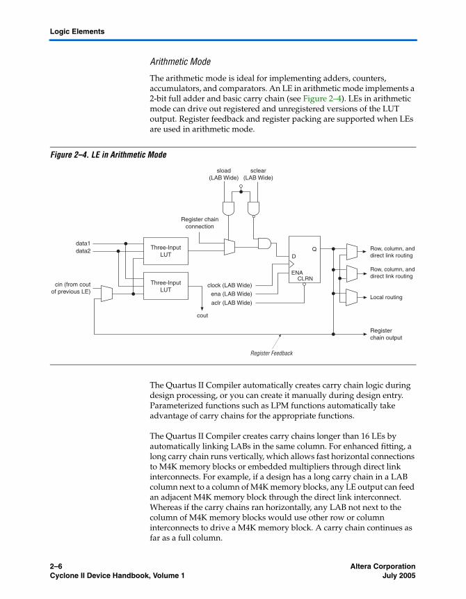
Arithmetic Mode
The arithmetic mode is ideal for implementing adders, counters, accumulators, and comparators. An LE in arithmetic mode implements a 2-bit full adder and basic carry chain (see Figure 2–4). LEs in arithmetic mode can drive out registered and unregistered versions of the LUT output. Register feedback and register packing are supported when LEs are used in arithmetic mode.
Figure 2–4. LE in Arithmetic Mode
The Quartus II Compiler automatically creates carry chain logic during design processing, or you can create it manually during design entry. Parameterized functions such as LPM functions automatically take advantage of carry chains for the appropriate functions.
The Quartus II Compiler creates carry chains longer than 16 LEs by automatically linking LABs in the same column. For enhanced fitting, a long carry chain runs vertically, which allows fast horizontal connections to M4K memory blocks or embedded multipliers through direct link interconnects. For example, if a design has a long carry chain in a LAB column next to a column of M4K memory blocks, any LE output can feed an adjacent M4K memory block through the direct link interconnect. Whereas if the carry chains ran horizontally, any LAB not next to the column of M4K memory blocks would use other row or column interconnects to drive a M4K memory block. A carry chain continues as far as a full column.
clock (LAB Wide)
ena (LAB Wide)
aclr (LAB Wide)
CLRN
DQ
ENA
Register chainconnection
sclear(LAB Wide)
sload(LAB Wide)
Registerchain output
Row, column, anddirect link routing
Row, column, anddirect link routing
Local routing
Register Feedback
Three-InputLUT
Three-InputLUT
cin (from coutof previous LE)
data2data1
cout
2–6 Altera CorporationCyclone II Device Handbook, Volume 1 July 2005
Cyclone II Architecture
Logic Array Blocks
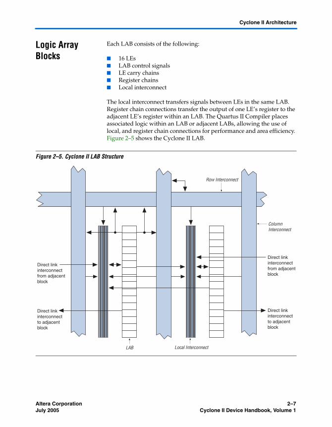
Each LAB consists of the following:
■ 16 LEs■ LAB control signals■ LE carry chains■ Register chains■ Local interconnect
The local interconnect transfers signals between LEs in the same LAB. Register chain connections transfer the output of one LE’s register to the adjacent LE’s register within an LAB. The Quartus II Compiler places associated logic within an LAB or adjacent LABs, allowing the use of local, and register chain connections for performance and area efficiency. Figure 2–5 shows the Cyclone II LAB.
Figure 2–5. Cyclone II LAB Structure
Direct linkinterconnectfrom adjacentblock
Direct linkinterconnectto adjacentblock
Row Interconnect
Column Interconnect
Local InterconnectLAB
Direct linkinterconnectfrom adjacentblock
Direct linkinterconnectto adjacentblock
Altera Corporation 2–7July 2005 Cyclone II Device Handbook, Volume 1
Logic Array Blocks
LAB Interconnects
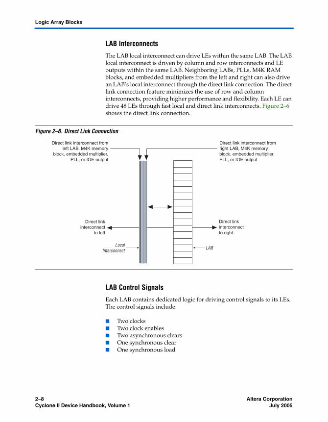
The LAB local interconnect can drive LEs within the same LAB. The LAB local interconnect is driven by column and row interconnects and LE outputs within the same LAB. Neighboring LABs, PLLs, M4K RAM blocks, and embedded multipliers from the left and right can also drive an LAB’s local interconnect through the direct link connection. The direct link connection feature minimizes the use of row and column interconnects, providing higher performance and flexibility. Each LE can drive 48 LEs through fast local and direct link interconnects. Figure 2–6 shows the direct link connection.
Figure 2–6. Direct Link Connection
LAB Control Signals
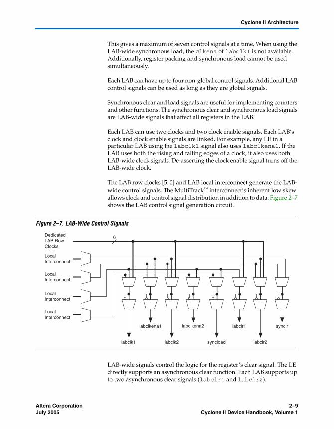
Each LAB contains dedicated logic for driving control signals to its LEs. The control signals include:
■ Two clocks■ Two clock enables■ Two asynchronous clears■ One synchronous clear■ One synchronous load
LAB
Direct linkinterconnectto right
Direct link interconnect fromright LAB, M4K memoryblock, embedded multiplier,PLL, or IOE output
Direct link interconnect fromleft LAB, M4K memory
block, embedded multiplier,PLL, or IOE output
LocalInterconnect
Direct linkinterconnect
to left
2–8 Altera CorporationCyclone II Device Handbook, Volume 1 July 2005
Cyclone II Architecture
This gives a maximum of seven control signals at a time. When using the LAB-wide synchronous load, the clkena of labclk1 is not available. Additionally, register packing and synchronous load cannot be used simultaneously.
Each LAB can have up to four non-global control signals. Additional LAB control signals can be used as long as they are global signals.
Synchronous clear and load signals are useful for implementing counters and other functions. The synchronous clear and synchronous load signals are LAB-wide signals that affect all registers in the LAB.
Each LAB can use two clocks and two clock enable signals. Each LAB’s clock and clock enable signals are linked. For example, any LE in a particular LAB using the labclk1 signal also uses labclkena1. If the LAB uses both the rising and falling edges of a clock, it also uses both LAB-wide clock signals. De-asserting the clock enable signal turns off the LAB-wide clock.
The LAB row clocks [5..0] and LAB local interconnect generate the LAB-wide control signals. The MultiTrack™ interconnect’s inherent low skew allows clock and control signal distribution in addition to data. Figure 2–7 shows the LAB control signal generation circuit.
Figure 2–7. LAB-Wide Control Signals
LAB-wide signals control the logic for the register’s clear signal. The LE directly supports an asynchronous clear function. Each LAB supports up to two asynchronous clear signals (labclr1 and labclr2).
labclkena1
labclk2labclk1
labclkena2 labclr1
DedicatedLAB RowClocks
LocalInterconnect
LocalInterconnect
LocalInterconnect
LocalInterconnect
syncload
synclr
labclr2
6
Altera Corporation 2–9July 2005 Cyclone II Device Handbook, Volume 1
MultiTrack Interconnect
A LAB-wide asynchronous load signal to control the logic for the register’s preset signal is not available. The register preset is achieved by using a NOT gate push-back technique. Cyclone II devices can only support either a preset or asynchronous clear signal.
In addition to the clear port, Cyclone II devices provide a chip-wide reset pin (DEV_CLRn) that resets all registers in the device. An option set before compilation in the Quartus II software controls this pin. This chip-wide reset overrides all other control signals.
MultiTrack Interconnect
In the Cyclone II architecture, connections between LEs, M4K memory blocks, embedded multipliers, and device I/O pins are provided by the MultiTrack interconnect structure with DirectDrive™ technology. The MultiTrack interconnect consists of continuous, performance-optimized routing lines of different speeds used for inter- and intra-design block connectivity. The Quartus II Compiler automatically places critical paths on faster interconnects to improve design performance.
DirectDrive technology is a deterministic routing technology that ensures identical routing resource usage for any function regardless of placement within the device. The MultiTrack interconnect and DirectDrive technology simplify the integration stage of block-based designing by eliminating the re-optimization cycles that typically follow design changes and additions.
The MultiTrack interconnect consists of row (direct link, R4, and R24) and column (register chain, C4, and C16) interconnects that span fixed distances. A routing structure with fixed-length resources for all devices allows predictable and repeatable performance when migrating through different device densities.
Row Interconnects
Dedicated row interconnects route signals to and from LABs, PLLs, M4K memory blocks, and embedded multipliers within the same row. These row resources include:
■ Direct link interconnects between LABs and adjacent blocks■ R4 interconnects traversing four blocks to the right or left■ R24 interconnects for high-speed access across the length of the
device
2–10 Altera CorporationCyclone II Device Handbook, Volume 1 July 2005
Cyclone II Architecture
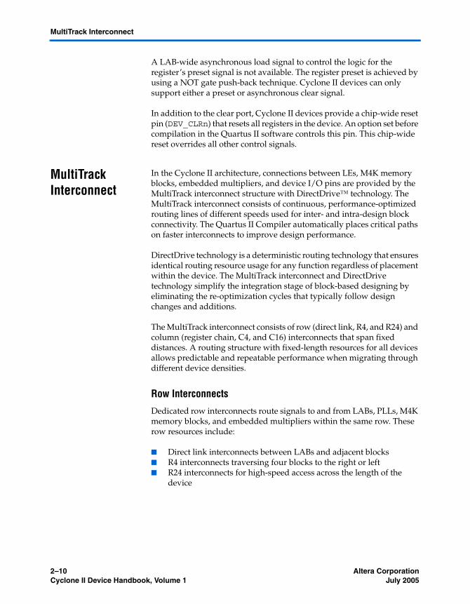
The direct link interconnect allows an LAB, M4K memory block, or embedded multiplier block to drive into the local interconnect of its left and right neighbors. Only one side of a PLL block interfaces with direct link and row interconnects. The direct link interconnect provides fast communication between adjacent LABs and/or blocks without using row interconnect resources.
The R4 interconnects span four LABs, three LABs and one M4K memory block, or three LABs and one embedded multiplier to the right or left of a source LAB. These resources are used for fast row connections in a four-LAB region. Every LAB has its own set of R4 interconnects to drive either left or right. Figure 2–8 shows R4 interconnect connections from an LAB. R4 interconnects can drive and be driven by LABs, M4K memory blocks, embedded multipliers, PLLs, and row IOEs. For LAB interfacing, a primary LAB or LAB neighbor (see Figure 2–8) can drive a given R4 interconnect. For R4 interconnects that drive to the right, the primary LAB and right neighbor can drive on to the interconnect. For R4 interconnects that drive to the left, the primary LAB and its left neighbor can drive on to the interconnect. R4 interconnects can drive other R4 interconnects to extend the range of LABs they can drive. Additionally, R4 interconnects can drive R24 interconnects, C4, and C16 interconnects for connections from one row to another.
Figure 2–8. R4 Interconnect Connections
Notes to Figure 2–8:(1) C4 interconnects can drive R4 interconnects.(2) This pattern is repeated for every LAB in the LAB row.
PrimaryLAB (2)
R4 InterconnectDriving Left
Adjacent LAB canDrive onto AnotherLAB's R4 Interconnect
C4 Column Interconnects (1)R4 InterconnectDriving Right
LABNeighbor
LABNeighbor
Altera Corporation 2–11July 2005 Cyclone II Device Handbook, Volume 1
MultiTrack Interconnect
R24 row interconnects span 24 LABs and provide the fastest resource for long row connections between non-adjacent LABs, M4K memory blocks, dedicated multipliers, and row IOEs. R24 row interconnects drive to other row or column interconnects at every fourth LAB. R24 row interconnects drive LAB local interconnects via R4 and C4 interconnects and do not drive directly to LAB local interconnects. R24 interconnects can drive R24, R4, C16, and C4 interconnects.
Column Interconnects
The column interconnect operates similar to the row interconnect. Each column of LABs is served by a dedicated column interconnect, which vertically routes signals to and from LABs, M4K memory blocks, embedded multipliers, and row and column IOEs. These column resources include:
■ Register chain interconnects within an LAB■ C4 interconnects traversing a distance of four blocks in an up and
down direction■ C16 interconnects for high-speed vertical routing through the device
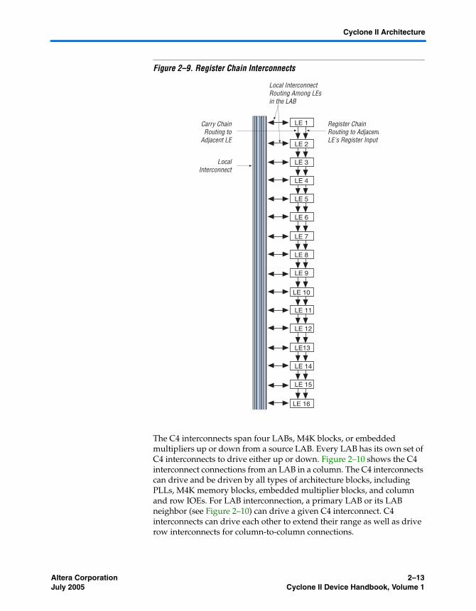
Cyclone II devices include an enhanced interconnect structure within LABs for routing LE output to LE input connections faster using register chain connections. The register chain connection allows the register output of one LE to connect directly to the register input of the next LE in the LAB for fast shift registers. The Quartus II Compiler automatically takes advantage of these resources to improve utilization and performance. Figure 2–9 shows the register chain interconnects.
2–12 Altera CorporationCyclone II Device Handbook, Volume 1 July 2005
Cyclone II Architecture
Figure 2–9. Register Chain Interconnects
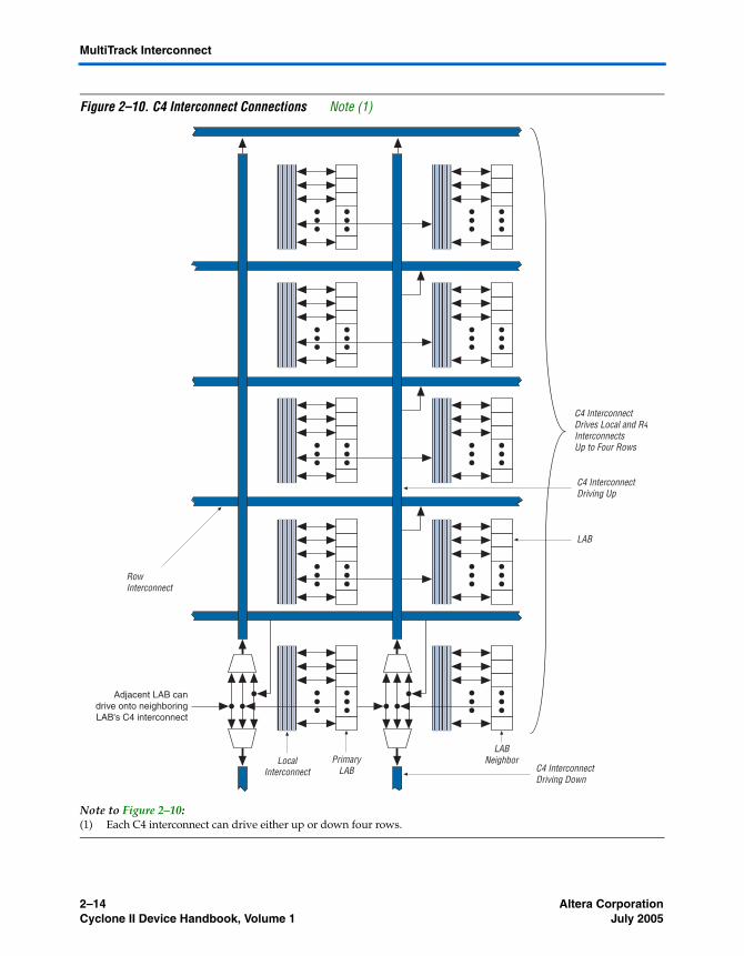
The C4 interconnects span four LABs, M4K blocks, or embedded multipliers up or down from a source LAB. Every LAB has its own set of C4 interconnects to drive either up or down. Figure 2–10 shows the C4 interconnect connections from an LAB in a column. The C4 interconnects can drive and be driven by all types of architecture blocks, including PLLs, M4K memory blocks, embedded multiplier blocks, and column and row IOEs. For LAB interconnection, a primary LAB or its LAB neighbor (see Figure 2–10) can drive a given C4 interconnect. C4 interconnects can drive each other to extend their range as well as drive row interconnects for column-to-column connections.
LE 1
LE 2
LE 3
LE 4
LE 5
LE 6
LE 7
LE 8
LE 9
LE 10
LE 11
LE 12
LE13
LE 14
LE 15
LE 16
Carry ChainRouting to
Adjacent LE
LocalInterconnect
Register ChainRouting to AdjacentLE's Register Input
Local InterconnectRouting Among LEsin the LAB
Altera Corporation 2–13July 2005 Cyclone II Device Handbook, Volume 1
MultiTrack Interconnect
Figure 2–10. C4 Interconnect Connections Note (1)
Note to Figure 2–10:(1) Each C4 interconnect can drive either up or down four rows.
C4 InterconnectDrives Local and R4InterconnectsUp to Four Rows
Adjacent LAB candrive onto neighboringLAB's C4 interconnect
C4 InterconnectDriving Up
C4 InterconnectDriving Down
LAB
RowInterconnect
LocalInterconnect
PrimaryLAB
LABNeighbor
2–14 Altera CorporationCyclone II Device Handbook, Volume 1 July 2005
Cyclone II Architecture
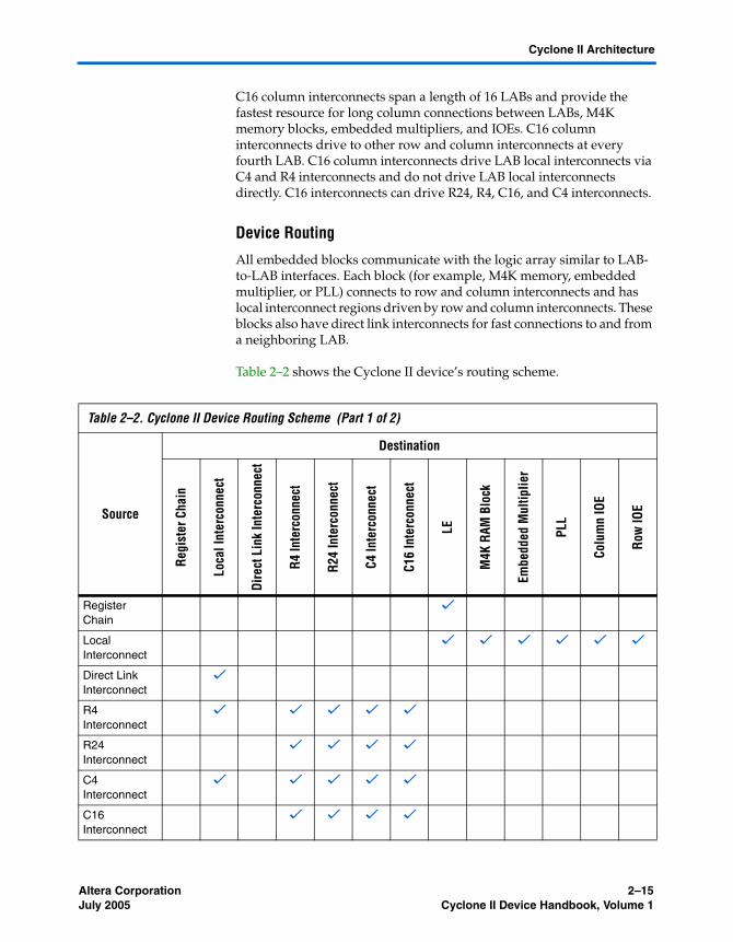
C16 column interconnects span a length of 16 LABs and provide the fastest resource for long column connections between LABs, M4K memory blocks, embedded multipliers, and IOEs. C16 column interconnects drive to other row and column interconnects at every fourth LAB. C16 column interconnects drive LAB local interconnects via C4 and R4 interconnects and do not drive LAB local interconnects directly. C16 interconnects can drive R24, R4, C16, and C4 interconnects.
Device Routing
All embedded blocks communicate with the logic array similar to LAB-to-LAB interfaces. Each block (for example, M4K memory, embedded multiplier, or PLL) connects to row and column interconnects and has local interconnect regions driven by row and column interconnects. These blocks also have direct link interconnects for fast connections to and from a neighboring LAB.
Table 2–2 shows the Cyclone II device’s routing scheme.
Table 2–2. Cyclone II Device Routing Scheme (Part 1 of 2)
Source
Destination
Regi
ster
Cha
in
Loca
l Int
erco
nnec
t
Dire
ct L
ink
Inte
rcon
nect
R4 In
terc
onne
ct
R24
Inte
rcon
nect
C4 In
terc
onne
ct
C16
Inte
rcon
nect
LE
M4K
RAM
Blo
ck
Embe
dded
Mul
tiplie
r
PLL
Colu
mn
IOE
Row
IOE
Register Chain
v
Local Interconnect
v v v v v v
Direct Link Interconnect
v
R4 Interconnect
v v v v v
R24 Interconnect
v v v v
C4 Interconnect
v v v v v
C16 Interconnect
v v v v
Altera Corporation 2–15July 2005 Cyclone II Device Handbook, Volume 1
Global Clock Network & Phase-Locked Loops
Global Clock Network & Phase-Locked Loops
Cyclone II devices provide global clock networks and up to four PLLs for a complete clock management solution. Cyclone II clock network features include:
■ Up to 16 global clock networks■ Up to four PLLs■ Global clock network dynamic clock source selection■ Global clock network dynamic enable and disable
LE v v v v v
M4K memory Block
v v v v
Embedded Multipliers
v v v v
PLL v v v
Column IOE v v
Row IOE v v v v
Table 2–2. Cyclone II Device Routing Scheme (Part 2 of 2)
Source
Destination
Regi
ster
Cha
in
Loca
l Int
erco
nnec
t
Dire
ct L
ink
Inte
rcon
nect
R4 In
terc
onne
ct
R24
Inte
rcon
nect
C4 In
terc
onne
ct
C16
Inte
rcon
nect
LE
M4K
RAM
Blo
ck
Embe
dded
Mul
tiplie
r
PLL
Colu
mn
IOE
Row
IOE
2–16 Altera CorporationCyclone II Device Handbook, Volume 1 July 2005
Cyclone II Architecture
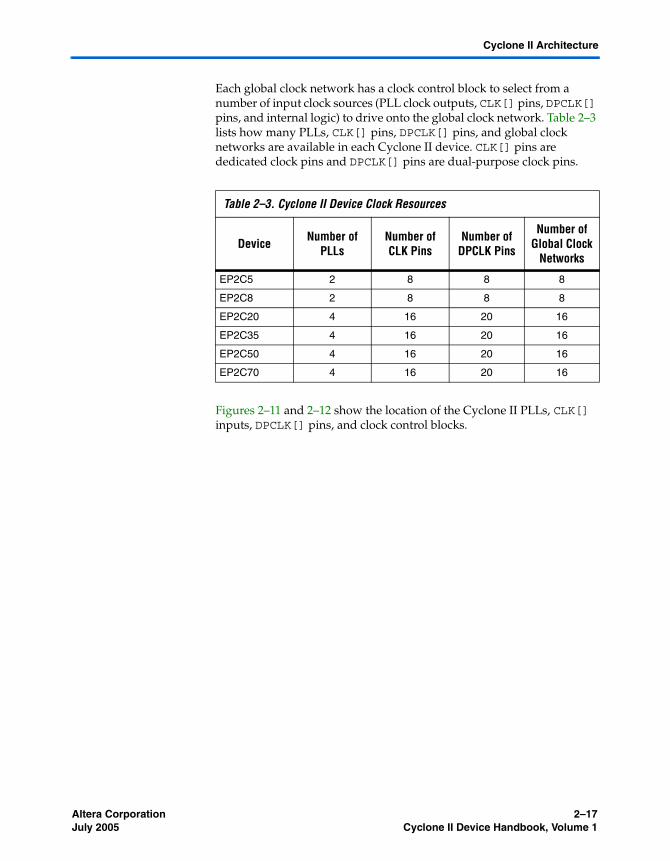
Each global clock network has a clock control block to select from a number of input clock sources (PLL clock outputs, CLK[] pins, DPCLK[] pins, and internal logic) to drive onto the global clock network. Table 2–3 lists how many PLLs, CLK[] pins, DPCLK[] pins, and global clock networks are available in each Cyclone II device. CLK[] pins are dedicated clock pins and DPCLK[] pins are dual-purpose clock pins.
Figures 2–11 and 2–12 show the location of the Cyclone II PLLs, CLK[] inputs, DPCLK[] pins, and clock control blocks.
Table 2–3. Cyclone II Device Clock Resources
Device Number of PLLs
Number of CLK Pins
Number of DPCLK Pins
Number of Global Clock
Networks
EP2C5 2 8 8 8
EP2C8 2 8 8 8
EP2C20 4 16 20 16
EP2C35 4 16 20 16
EP2C50 4 16 20 16
EP2C70 4 16 20 16
Altera Corporation 2–17July 2005 Cyclone II Device Handbook, Volume 1
Global Clock Network & Phase-Locked Loops
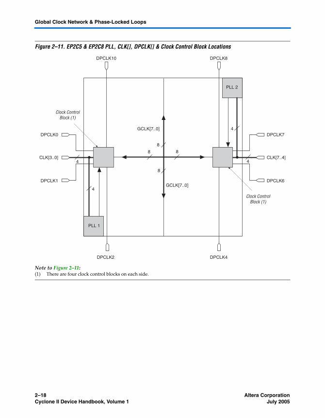
Figure 2–11. EP2C5 & EP2C8 PLL, CLK[], DPCLK[] & Clock Control Block Locations
Note to Figure 2–11:(1) There are four clock control blocks on each side.
PLL 2
CLK[7..4]
DPCLK7
DPCLK6
CLK[3..0]
DPCLK0
DPCLK1
DPCLK10 DPCLK8
DPCLK2
GCLK[7..0]
GCLK[7..0]
DPCLK4
PLL 1
8
8
8
8
Clock ControlBlock (1)
Clock ControlBlock (1)
4
4
4
4
2–18 Altera CorporationCyclone II Device Handbook, Volume 1 July 2005
Cyclone II Architecture
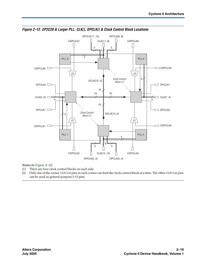
Figure 2–12. EP2C20 & Larger PLL, CLK[], DPCLK[] & Clock Control Block Locations
Notes to Figure 2–12:(1) There are four clock control blocks on each side.(2) Only one of the corner CDPCLK pins in each corner can feed the clock control block at a time. The other CDPCLK pins
can be used as general-purpose I/O pins.
PLL 4
PLL 3 PLL 2
CLK[7..4]
DPCLK7
CDPCLK5
CDPCLK4
DPCLK6
CLK[3..0]
DPCLK0
CDPCLK0
CDPCLK1
DPCLK1
CDPCLK7
DPCLK[9..8]DPCLK[11..10]
CLK[11..8]
GCLK[15..0]
GCLK[15..0]
PLL 1
CDPCLK6
CDPCLK2
DPCLK[5..4]DPCLK[3..2]
CLK[15..12] CDPCLK3
Clock ControlBlock (1)
Clock ControlBlock (1)
16 16
16
16
2 24
4
4
4
4
224
(2) (2)
(2) (2)
4
4
Altera Corporation 2–19July 2005 Cyclone II Device Handbook, Volume 1
Global Clock Network & Phase-Locked Loops
Dedicated Clock Pins
Larger Cyclone II devices (EP2C20 and larger devices) have 16 dedicated clock pins (CLK[15..0], four pins on each side of the device). Smaller Cyclone II devices (EP2C5 and EP2C8 devices) have eight dedicated clock pins (CLK[7..0], four pins on left and right sides of the device). These CLK pins drive the global clock network (GCLK), as shown in Figures 2–11 and 2–12.
If the dedicated clock pins are not used to feed the global clock networks, they can be used as general-purpose input pins to feed the logic array using the MultiTrack interconnect. However, if they are used as general-purpose input pins, they do not have support for an I/O register and must use LE-based registers in place of an I/O register.
Dual-Purpose Clock Pins
Cyclone II devices have either 20 dual-purpose clock pins, DPCLK[19..0] or 8 dual-purpose clock pins, DPCLK[7..0]. In the larger Cyclone II devices (EP2C20 devices and higher), there are 20 DPCLK pins; four on the left and right sides and six on the top and bottom of the device. The corner CDPCLK pins are first multiplexed before they drive into the clock control block. Since the signals pass through a multiplexer before feeding the clock control block, these signals incur more delay to the clock control block than other DPCLK pins that directly feed the clock control block. In the smaller Cyclone II devices (EP2C5 and EP2C8 devices), there are eight DPCLK pins; two on each side of the device (see Figures 2–11 and 2–12).
A programmable delay chain is available from the DPCLK pin to its fan-out destinations. To set the propagation delay from the DPCLK pin to its fan-out destinations, use the Input Delay from Dual-Purpose Clock Pin to Fan-Out Destinations assignment in the Quartus II software.
These dual-purpose pins can connect to the global clock network for high-fanout control signals such as clocks, asynchronous clears, presets, and clock enables, or protocol control signals such as TRDY and IRDY for PCI, or DQS signals for external memory interfaces.
2–20 Altera CorporationCyclone II Device Handbook, Volume 1 July 2005
Cyclone II Architecture
Global Clock Network
The 16 or 8 global clock networks drive throughout the entire device. Dedicated clock pins (CLK[]), PLL outputs, the logic array, and dual-purpose clock (DPCLK[]) pins can also drive the global clock network.
The global clock network can provide clocks for all resources within the device, such as IOEs, LEs, memory blocks, and embedded multipliers. The global clock lines can also be used for control signals, such as clock enables and synchronous or asynchronous clears fed from the external pin, or DQS signals for DDR SDRAM or QDRII SRAM interfaces. Internal logic can also drive the global clock network for internally generated global clocks and asynchronous clears, clock enables, or other control signals with large fan-out.
Clock Control Block
There is a clock control block for each global clock network available in Cyclone II devices. The clock control blocks are arranged on the device periphery and there are a maximum of 16 clock control blocks available per Cyclone II device. The larger Cyclone II devices (EP2C20 devices and larger) have 16 clock control blocks, four on each side of the device. The smaller Cyclone II devices (EP2C5 and EP2C8 devices) have eight clock control blocks, four on the left and right sides of the device.
The control block has these functions:
■ Dynamic global clock network clock source selection ■ Dynamic enable/disable of the global clock network
In Cyclone II devices, the dedicated CLK[] pins, PLL counter outputs, DPCLK[] pins, and internal logic can all feed the clock control block. The output from the clock control block in turn feeds the corresponding global clock network.
The following sources can be inputs to a given clock control block:
■ Four clock pins on the same side as the clock control block■ Three PLL clock outputs from a PLL■ Four DPCLK pins (including CDPCLK pins) on the same side as the
clock control block■ Four internally-generated signals
Altera Corporation 2–21July 2005 Cyclone II Device Handbook, Volume 1
Global Clock Network & Phase-Locked Loops
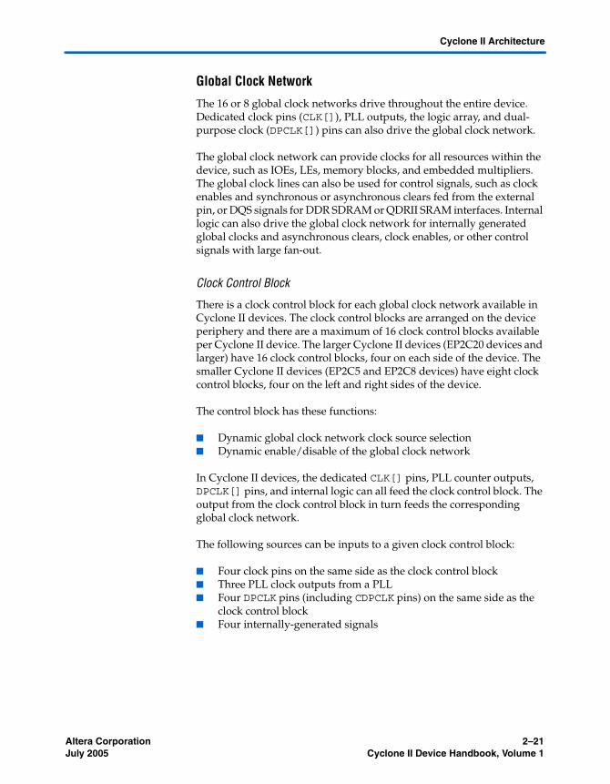
Of the sources listed, only two clock pins, two PLL clock outputs, one DPCLK pin, and one internally-generated signal are chosen to drive into a clock control block. Figure 2–13 shows a more detailed diagram of the clock control block. Out of these six inputs, the two clock input pins and two PLL outputs can be dynamic selected to feed a global clock network. The clock control block supports static selection of DPCLK and the signal from internal logic.
Figure 2–13. Clock Control Block
Notes to Figure 2–13:(1) The CLKSWITCH signal can either be set through the configuration file or it can be dynamically set when using the
manual PLL switchover feature. The output of the multiplexer is the input reference clock (fIN) for the PLL. (2) The CLKSELECT[1..0] signals are fed by internal logic and can be used to dynamically select the clock source for
the global clock network when the device is in user mode.(3) The static clock select signals are set in the configuration file and cannot be dynamically controlled when the device
is in user mode.(4) Internal logic can be used to enabled or disabled the global clock network in user mode.
CLKSWITCH (1)
Static Clock Select (3)
Static ClockSelect (3)
Internal Logic
Clock Control Block
DPCLK orCDPCLK
CLKSELECT[1..0] (2) CLKENA (4)
inclk1inclk0
CLK[n + 3]CLK[n + 2]CLK[n + 1]
CLK[n]
fINC0C1C2
PLL
GlobalClock
Enable/Disable
(3)
2–22 Altera CorporationCyclone II Device Handbook, Volume 1 July 2005
Cyclone II Architecture
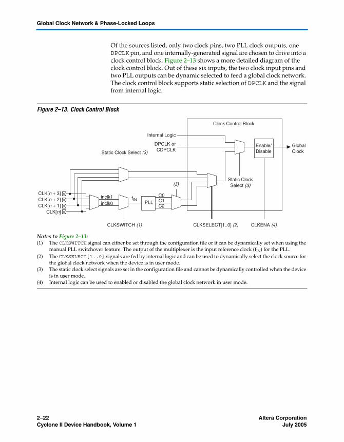
Global Clock Network Distribution
Cyclone II devices contains 16 global clock networks. The device uses multiplexers with these clocks to form six-bit buses to drive column IOE clocks, LAB row clocks, or row IOE clocks (see Figure 2–14). Another multiplexer at the LAB level selects two of the six LAB row clocks to feed the LE registers within the LAB.
Figure 2–14. Global Clock Network Multiplexers
LAB row clocks can feed LEs, M4K memory blocks, and embedded multipliers. The LAB row clocks also extend to the row I/O clock regions.
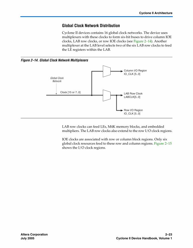
IOE clocks are associated with row or column block regions. Only six global clock resources feed to these row and column regions. Figure 2–15 shows the I/O clock regions.
Clock [15 or 7..0]
Row I/O RegionIO_CLK [5..0]
Column I/O RegionIO_CLK [5..0]
LAB Row Clock LABCLK[5..0]
Global ClockNetwork
Altera Corporation 2–23July 2005 Cyclone II Device Handbook, Volume 1
Global Clock Network & Phase-Locked Loops
Figure 2–15. LAB & I/O Clock Regions
f For more information on the global clock network and the clock control block, see the PLLs in Cyclone II Devices chapter in Volume 1 of the Cyclone II Device Handbook.
Column I/O Clock RegionIO_CLK[5..0]
Column I/O Clock RegionIO_CLK[5..0]
6
6
I/O Clock Regions
I/O Clock Regions
8 or 16
Global ClockNetwork
Row I/O ClockRegionIO_CLK[5..0]
Cyclone Logic Array
6
6
LAB Row Clockslabclk[5..0]
LAB Row Clockslabclk[5..0]
LAB Row Clockslabclk[5..0]
LAB Row Clockslabclk[5..0]
LAB Row Clockslabclk[5..0]
LAB Row Clockslabclk[5..0]
6
6
6
6
6
6
6
6 6
6
2–24 Altera CorporationCyclone II Device Handbook, Volume 1 July 2005
Cyclone II Architecture
PLLs
Cyclone II PLLs provide general-purpose clocking as well as support for the following features:
■ Clock multiplication and division■ Phase shifting■ Programmable duty cycle■ Up to three internal clock outputs■ One dedicated external clock output■ Clock outputs for differential I/O support■ Manual clock switchover■ Gated lock signal■ Three different clock feedback modes■ Control signals
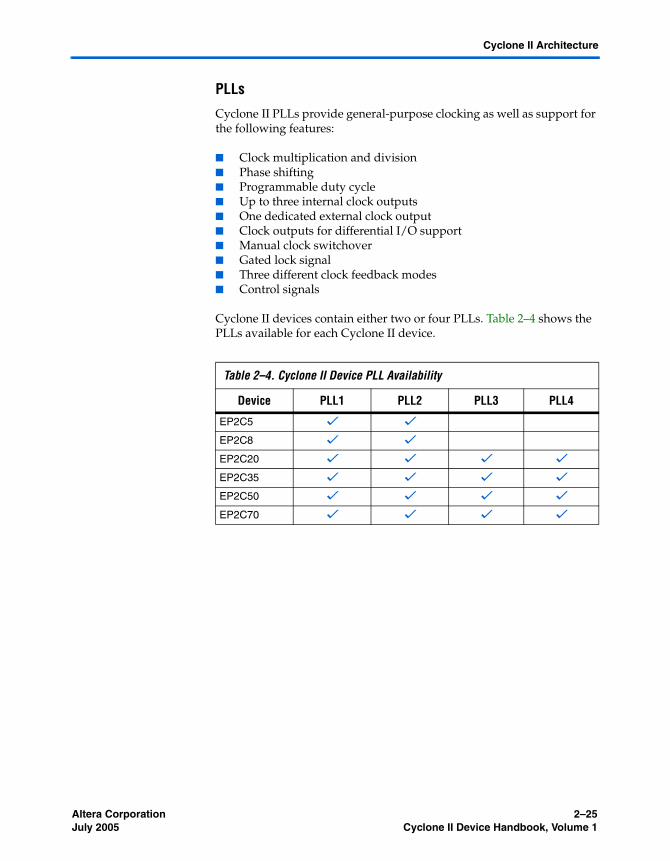
Cyclone II devices contain either two or four PLLs. Table 2–4 shows the PLLs available for each Cyclone II device.
Table 2–4. Cyclone II Device PLL Availability
Device PLL1 PLL2 PLL3 PLL4
EP2C5 v v
EP2C8 v v
EP2C20 v v v v
EP2C35 v v v v
EP2C50 v v v v
EP2C70 v v v v
Altera Corporation 2–25July 2005 Cyclone II Device Handbook, Volume 1
Global Clock Network & Phase-Locked Loops
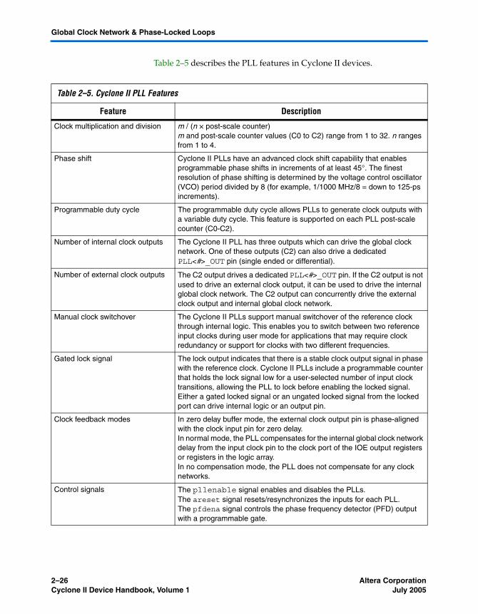
Table 2–5 describes the PLL features in Cyclone II devices.
Table 2–5. Cyclone II PLL Features
Feature Description
Clock multiplication and division m / (n × post-scale counter) m and post-scale counter values (C0 to C2) range from 1 to 32. n ranges from 1 to 4.
Phase shift Cyclone II PLLs have an advanced clock shift capability that enables programmable phase shifts in increments of at least 45°. The finest resolution of phase shifting is determined by the voltage control oscillator (VCO) period divided by 8 (for example, 1/1000 MHz/8 = down to 125-ps increments).
Programmable duty cycle The programmable duty cycle allows PLLs to generate clock outputs with a variable duty cycle. This feature is supported on each PLL post-scale counter (C0-C2).
Number of internal clock outputs The Cyclone II PLL has three outputs which can drive the global clock network. One of these outputs (C2) can also drive a dedicated PLL<#>_OUT pin (single ended or differential).
Number of external clock outputs The C2 output drives a dedicated PLL<#>_OUT pin. If the C2 output is not used to drive an external clock output, it can be used to drive the internal global clock network. The C2 output can concurrently drive the external clock output and internal global clock network.
Manual clock switchover The Cyclone II PLLs support manual switchover of the reference clock through internal logic. This enables you to switch between two reference input clocks during user mode for applications that may require clock redundancy or support for clocks with two different frequencies.
Gated lock signal The lock output indicates that there is a stable clock output signal in phase with the reference clock. Cyclone II PLLs include a programmable counter that holds the lock signal low for a user-selected number of input clock transitions, allowing the PLL to lock before enabling the locked signal. Either a gated locked signal or an ungated locked signal from the locked port can drive internal logic or an output pin.
Clock feedback modes In zero delay buffer mode, the external clock output pin is phase-aligned with the clock input pin for zero delay. In normal mode, the PLL compensates for the internal global clock network delay from the input clock pin to the clock port of the IOE output registers or registers in the logic array.In no compensation mode, the PLL does not compensate for any clock networks.
Control signals The pllenable signal enables and disables the PLLs. The areset signal resets/resynchronizes the inputs for each PLL. The pfdena signal controls the phase frequency detector (PFD) output with a programmable gate.
2–26 Altera CorporationCyclone II Device Handbook, Volume 1 July 2005
Cyclone II Architecture
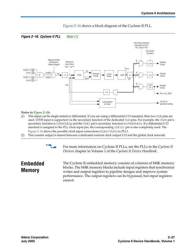
Figure 2–16 shows a block diagram of the Cyclone II PLL.
Figure 2–16. Cyclone II PLL Note (1)
Notes to Figure 2–16:(1) This input can be single-ended or differential. If you are using a differential I/O standard, then two CLK pins are
used. LVDS input is supported via the secondary function of the dedicated CLK pins. For example, the CLK0 pin’s secondary function is LVDSCLK1p and the CLK1 pin’s secondary function is LVDSCLK1n. If a differential I/O standard is assigned to the PLL clock input pin, the corresponding CLK(n) pin is also completely used. The Figure 2–16 shows the possible clock input connections (CLK0/CLK1) to PLL1.
(2) This counter output is shared between a dedicated external clock output I/O and the global clock network.
f For more information on Cyclone II PLLs, see the PLLs in the Cyclone II Devices chapter in Volume 1 of the Cyclone II Device Handbook.
Embedded Memory
The Cyclone II embedded memory consists of columns of M4K memory blocks. The M4K memory blocks include input registers that synchronize writes and output registers to pipeline designs and improve system performance. The output registers can be bypassed, but input registers cannot.
PFD LoopFilter
Lock Detect& Filter
VCOChargePump
÷c0
÷c1
÷c2
÷m
÷n
GlobalClock
GlobalClock
GlobalClock
To I/O orgeneral routing
PLL<#>_OUT
Post-ScaleCounters
VCO Phase SelectionSelectable at Each PLL Output Port
CLK1
CLK3
CLK2 (1)
CLK0 (1)inclk0
inclk1
up
down
8
8
8
fVCO
fFB
fIN
ReferenceInput ClockfREF = fIN /n
(2)
Manual ClockSwitchover
Select Signal
÷k
(3)
Altera Corporation 2–27July 2005 Cyclone II Device Handbook, Volume 1
Embedded Memory
Each M4K block can implement various types of memory with or without parity, including true dual-port, simple dual-port, and single-port RAM, ROM, and first-in first-out (FIFO) buffers. The M4K blocks support the following features:
■ 4,608 RAM bits■ 250-MHz performance■ True dual-port memory■ Simple dual-port memory■ Single-port memory■ Byte enable■ Parity bits■ Shift register■ FIFO buffer■ ROM■ Various clock modes■ Address clock enable
1 Violating the setup or hold time on the memory block address registers could corrupt memory contents. This applies to both read and write operations.
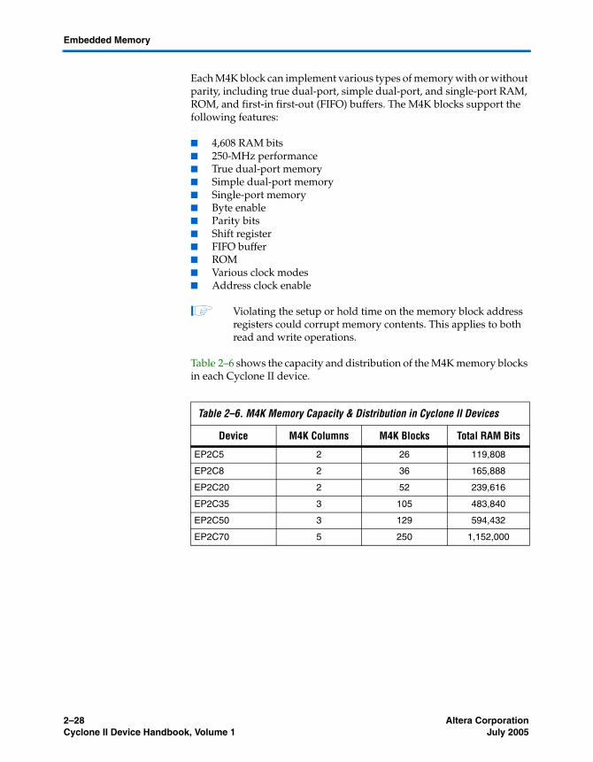
Table 2–6 shows the capacity and distribution of the M4K memory blocks in each Cyclone II device.
Table 2–6. M4K Memory Capacity & Distribution in Cyclone II Devices
Device M4K Columns M4K Blocks Total RAM Bits
EP2C5 2 26 119,808
EP2C8 2 36 165,888
EP2C20 2 52 239,616
EP2C35 3 105 483,840
EP2C50 3 129 594,432
EP2C70 5 250 1,152,000
2–28 Altera CorporationCyclone II Device Handbook, Volume 1 July 2005
Cyclone II Architecture
Table 2–7 summarizes the features supported by the M4K memory.
Table 2–7. M4K Memory Features
Feature Description
Maximum performance (1) 250 MHz
Total RAM bits per M4K block (including parity bits) 4,608
Configurations supported 4K × 12K × 21K × 4512 × 8512 × 9256 × 16256 × 18128 × 32 (not available in true dual-port mode)128 × 36 (not available in true dual-port mode)
Parity bits One parity bit for each byte. The parity bit, along with internal user logic, can implement parity checking for error detection to ensure data integrity.
Byte enable M4K blocks support byte writes when the write port has a data width of 1, 2, 4, 8, 9, 16, 18, 32, or 36 bits. The byte enables allow the input data to be masked so the device can write to specific bytes. The unwritten bytes retain the previous written value.
Packed mode Two single-port memory blocks can be packed into a single M4K block if each of the two independent block sizes are equal to or less than half of the M4K block size, and each of the single-port memory blocks is configured in single-clock mode.
Address clock enable M4K blocks support address clock enable, which is used to hold the previous address value for as long as the signal is enabled. This feature is useful in handling misses in cache applications.
Memory initialization file (.mif) When configured as RAM or ROM, you can use an initialization file to pre-load the memory contents.
Power-up condition Outputs cleared
Register clears Output registers only
Same-port read-during-write New data available at positive clock edge
Mixed-port read-during-write Old data available at positive clock edge
Note to Table 2–7:(1) Maximum performance information is preliminary until device characterization.
Altera Corporation 2–29July 2005 Cyclone II Device Handbook, Volume 1
Embedded Memory
Clear Signals
When applied to input registers, the asynchronous clear signal for the TriMatrix™ embedded memory immediately clears the input registers. However, the output of the memory block does not show the effects until the next clock edge. When applied to output registers, the asynchronous clear signal clears the output registers and the effects are seen immediately.
Memory Modes
Table 2–8 summarizes the different memory modes supported by the M4K memory blocks.
Table 2–8. M4K Memory Modes
Memory Mode Description
Single-port memory M4K blocks support single-port mode, used when simultaneous reads and writes are not required. Single-port memory supports non-simultaneous reads and writes.
Simple dual-port memory Simple dual-port memory supports a simultaneous read and write.
Simple dual-port with mixed width
Simple dual-port memory mode with different read and write port widths.
True dual-port memory True dual-port mode supports any combination of two-port operations: two reads, two writes, or one read and one write at two different clock frequencies.
True dual-port with mixed width
True dual-port mode with different read and write port widths.
Embedded shift register M4K memory blocks are used to implement shift registers. Data is written into each address location at the falling edge of the clock and read from the address at the rising edge of the clock.
ROM The M4K memory blocks support ROM mode. A MIF initializes the ROM contents of these blocks.
FIFO buffers A single clock or dual clock FIFO may be implemented in the M4K blocks. Simultaneous read and write from an empty FIFO buffer is not supported.
2–30 Altera CorporationCyclone II Device Handbook, Volume 1 July 2005
Cyclone II Architecture
Clock Modes
Table 2–9 summarizes the different clock modes supported by the M4K memory.
Table 2–10 shows which clock modes are supported by all M4K blocks when configured in the different memory modes.
M4K Routing Interface
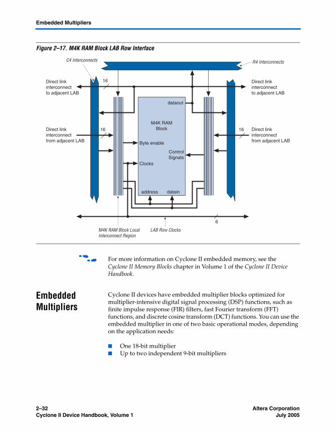
The R4, C4, and direct link interconnects from adjacent LABs drive the M4K block local interconnect. The M4K blocks can communicate with LABs on either the left or right side through these row resources or with LAB columns on either the right or left with the column resources. Up to 16 direct link input connections to the M4K block are possible from the left adjacent LAB and another 16 possible from the right adjacent LAB. M4K block outputs can also connect to left and right LABs through each 16 direct link interconnects. Figure 2–17 shows the M4K block to logic array interface.
Table 2–9. M4K Clock Modes
Clock Mode Description
Independent In this mode, a separate clock is available for each port (ports A and B). Clock A controls all registers on the port A side, while clock B controls all registers on the port B side.
Input/output On each of the two ports, A or B, one clock controls all registers for inputs into the memory block: data input, wren, and address. The other clock controls the block’s data output registers.
Read/write Up to two clocks are available in this mode. The write clock controls the block’s data inputs, wraddress, and wren. The read clock controls the data output, rdaddress, and rden.
Single In this mode, a single clock, together with clock enable, is used to control all registers of the memory block. Asynchronous clear signals for the registers are not supported.
Table 2–10. Cyclone II M4K Memory Clock Modes
Clocking Modes True Dual-Port Mode
Simple Dual-Port Mode Single-Port Mode
Independent v
Input/output v v v
Read/write v
Single clock v v v
Altera Corporation 2–31July 2005 Cyclone II Device Handbook, Volume 1
Embedded Multipliers
Figure 2–17. M4K RAM Block LAB Row Interface
f For more information on Cyclone II embedded memory, see the Cyclone II Memory Blocks chapter in Volume 1 of the Cyclone II Device Handbook.
Embedded Multipliers
Cyclone II devices have embedded multiplier blocks optimized for multiplier-intensive digital signal processing (DSP) functions, such as finite impulse response (FIR) filters, fast Fourier transform (FFT) functions, and discrete cosine transform (DCT) functions. You can use the embedded multiplier in one of two basic operational modes, depending on the application needs:
■ One 18-bit multiplier■ Up to two independent 9-bit multipliers
dataout
M4K RAMBlock
datainaddress
16
16 16Direct link interconnectfrom adjacent LAB
Direct link interconnectto adjacent LAB
Direct link interconnectfrom adjacent LAB
Direct link interconnectto adjacent LAB
M4K RAM Block LocalInterconnect Region
C4 Interconnects R4 Interconnects
LAB Row Clocks
Clocks
Byte enable
ControlSignals
6
2–32 Altera CorporationCyclone II Device Handbook, Volume 1 July 2005
Cyclone II Architecture
Embedded multipliers can operate at up to 250 MHz (for the fastest speed grade) for 18 × 18 and 9 × 9 multiplications when using both input and output registers.
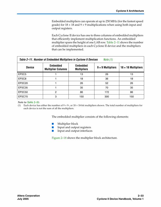
Each Cyclone II device has one to three columns of embedded multipliers that efficiently implement multiplication functions. An embedded multiplier spans the height of one LAB row. Table 2–11 shows the number of embedded multipliers in each Cyclone II device and the multipliers that can be implemented.
The embedded multiplier consists of the following elements:
■ Multiplier block■ Input and output registers■ Input and output interfaces
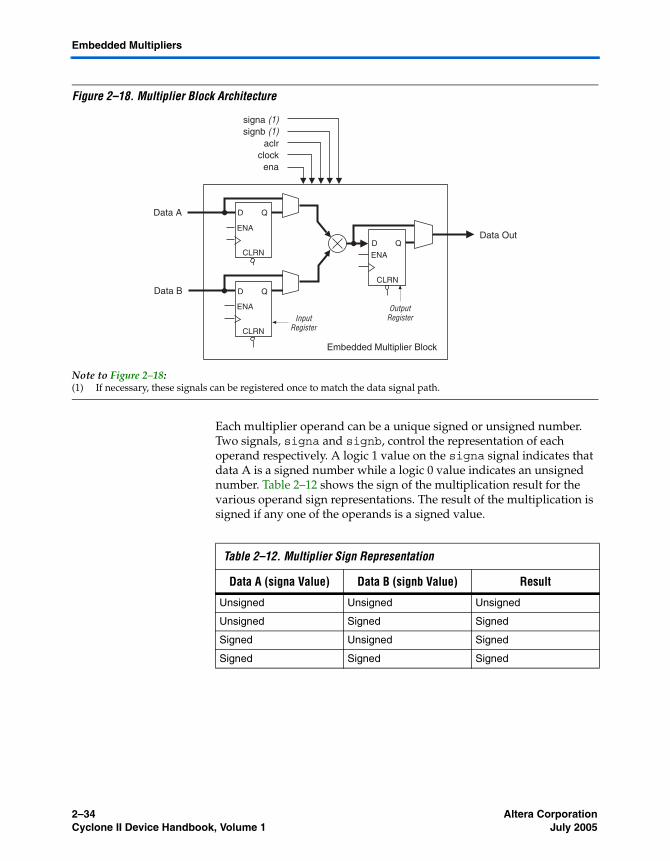
Figure 2–18 shows the multiplier block architecture.
Table 2–11. Number of Embedded Multipliers in Cyclone II Devices Note (1)
Device Embedded Multiplier Columns
Embedded Multipliers 9 × 9 Multipliers 18 × 18 Multipliers
EP2C5 1 13 26 13
EP2C8 1 18 36 18
EP2C20 1 26 52 26
EP2C35 1 35 70 35
EP2C50 2 86 172 86
EP2C70 3 150 300 150
Note to Table 2–11:(1) Each device has either the number of 9 × 9-, or 18 × 18-bit multipliers shown. The total number of multipliers for
each device is not the sum of all the multipliers.
Altera Corporation 2–33July 2005 Cyclone II Device Handbook, Volume 1
Embedded Multipliers
Figure 2–18. Multiplier Block Architecture
Note to Figure 2–18:(1) If necessary, these signals can be registered once to match the data signal path.
Each multiplier operand can be a unique signed or unsigned number. Two signals, signa and signb, control the representation of each operand respectively. A logic 1 value on the signa signal indicates that data A is a signed number while a logic 0 value indicates an unsigned number. Table 2–12 shows the sign of the multiplication result for the various operand sign representations. The result of the multiplication is signed if any one of the operands is a signed value.
CLRN
D Q
ENA
Data A
Data B
aclrclock
ena
signa (1)signb (1)
CLRN
D Q
ENA
CLRN
D Q
ENAData Out
Embedded Multiplier Block
OutputRegisterInput
Register
Table 2–12. Multiplier Sign Representation
Data A (signa Value) Data B (signb Value) Result
Unsigned Unsigned Unsigned
Unsigned Signed Signed
Signed Unsigned Signed
Signed Signed Signed
2–34 Altera CorporationCyclone II Device Handbook, Volume 1 July 2005
Cyclone II Architecture
There is only one signa and one signb signal for each dedicated multiplier. Therefore, all of the data A inputs feeding the same dedicated multiplier must have the same sign representation. Similarly, all of the data B inputs feeding the same dedicated multiplier must have the same sign representation. The signa and signb signals can be changed dynamically to modify the sign representation of the input operands at run time. The multiplier offers full precision regardless of the sign representation and can be registered using dedicated registers located at the input register stage.
Multiplier Modes
Table 2–13 summarizes the different modes that the embedded multipliers can operate in.
Table 2–13. Embedded Multiplier Modes
Multiplier Mode Description
18-bit Multiplier An embedded multiplier can be configured to support a single 18 × 18 multiplier for operand widths up to 18 bits. All 18-bit multiplier inputs and results can be registered independently. The multiplier operands can accept signed integers, unsigned integers, or a combination of both.
9-bit Multiplier An embedded multiplier can be configured to support two 9 × 9 independent multipliers for operand widths up to 9-bits. Both 9-bit multiplier inputs and results can be registered independently. The multiplier operands can accept signed integers, unsigned integers or a combination of both. There is only one signa signal to control the sign representation of both data A inputs and one signb signal to control the sign representation of both data B inputs of the 9-bit multipliers within the same dedicated multiplier.
Altera Corporation 2–35July 2005 Cyclone II Device Handbook, Volume 1
Embedded Multipliers
Embedded Multiplier Routing Interface
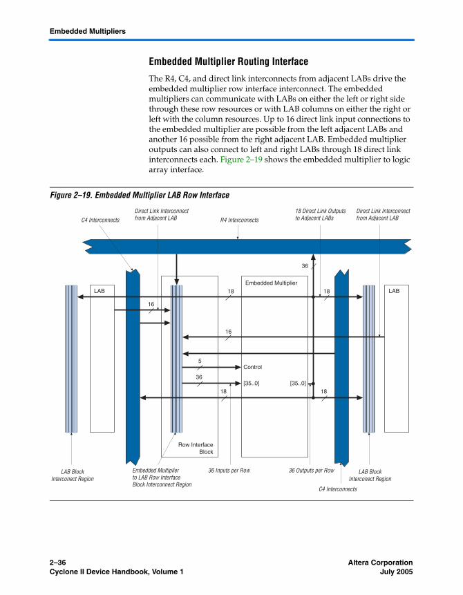
The R4, C4, and direct link interconnects from adjacent LABs drive the embedded multiplier row interface interconnect. The embedded multipliers can communicate with LABs on either the left or right side through these row resources or with LAB columns on either the right or left with the column resources. Up to 16 direct link input connections to the embedded multiplier are possible from the left adjacent LABs and another 16 possible from the right adjacent LAB. Embedded multiplier outputs can also connect to left and right LABs through 18 direct link interconnects each. Figure 2–19 shows the embedded multiplier to logic array interface.
Figure 2–19. Embedded Multiplier LAB Row Interface
LAB LAB
Row InterfaceBlock
Embedded Multiplier
16
[35..0][35..0]
Embedded Multiplierto LAB Row InterfaceBlock Interconnect Region
36 Inputs per Row 36 Outputs per Row
R4 InterconnectsC4 Interconnects
C4 Interconnects
Direct Link Interconnectfrom Adjacent LAB
18 Direct Link Outputsto Adjacent LABs
Direct Link Interconnectfrom Adjacent LAB
18 18
36
36
Control5
18 18
16
LAB BlockInterconect Region
LAB BlockInterconect Region
2–36 Altera CorporationCyclone II Device Handbook, Volume 1 July 2005
Cyclone II Architecture
There are five dynamic control input signals that feed the embedded multiplier: signa, signb, clk, clkena, and aclr. signa and signb can be registered to match the data signal input path. The same clk, clkena, and aclr signals feed all registers within a single embedded multiplier.
f For more information on Cyclone II embedded multipliers, see the Embedded Multipliers in Cyclone II Devices chapter.
I/O Structure & Features
IOEs support many features, including:
■ Differential and single-ended I/O standards■ 3.3-V, 64- and 32-bit, 66- and 33-MHz PCI compliance■ Joint Test Action Group (JTAG) boundary-scan test (BST) support■ Output drive strength control■ Weak pull-up resistors during configuration■ Tri-state buffers■ Bus-hold circuitry■ Programmable pull-up resistors in user mode■ Programmable input and output delays■ Open-drain outputs■ DQ and DQS I/O pins ■ VREF pins
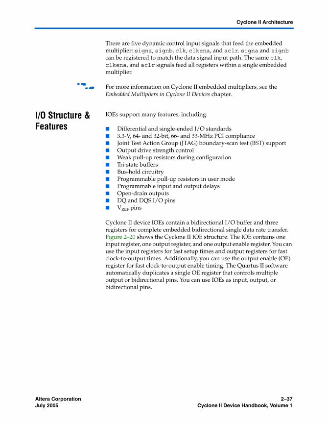
Cyclone II device IOEs contain a bidirectional I/O buffer and three registers for complete embedded bidirectional single data rate transfer. Figure 2–20 shows the Cyclone II IOE structure. The IOE contains one input register, one output register, and one output enable register. You can use the input registers for fast setup times and output registers for fast clock-to-output times. Additionally, you can use the output enable (OE) register for fast clock-to-output enable timing. The Quartus II software automatically duplicates a single OE register that controls multiple output or bidirectional pins. You can use IOEs as input, output, or bidirectional pins.
Altera Corporation 2–37July 2005 Cyclone II Device Handbook, Volume 1
I/O Structure & Features
Figure 2–20. Cyclone II IOE Structure
Note to Figure 2–20:(1) There are two paths available for combinational or registered inputs to the logic
array. Each path contains a unique programmable delay chain.
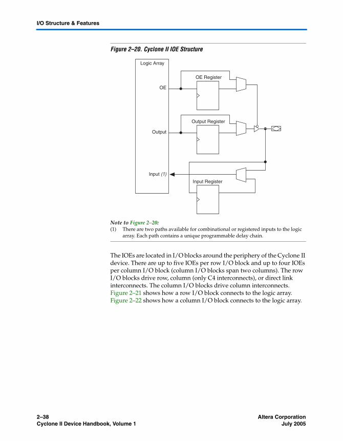
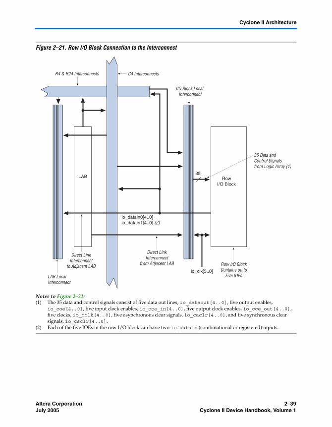
The IOEs are located in I/O blocks around the periphery of the Cyclone II device. There are up to five IOEs per row I/O block and up to four IOEs per column I/O block (column I/O blocks span two columns). The row I/O blocks drive row, column (only C4 interconnects), or direct link interconnects. The column I/O blocks drive column interconnects. Figure 2–21 shows how a row I/O block connects to the logic array. Figure 2–22 shows how a column I/O block connects to the logic array.
Output Register
Output
Input (1)
OE Register
OE
Input Register
Logic Array
2–38 Altera CorporationCyclone II Device Handbook, Volume 1 July 2005
Cyclone II Architecture
Figure 2–21. Row I/O Block Connection to the Interconnect
Notes to Figure 2–21:(1) The 35 data and control signals consist of five data out lines, io_dataout[4..0], five output enables,
io_coe[4..0], five input clock enables, io_cce_in[4..0], five output clock enables, io_cce_out[4..0], five clocks, io_cclk[4..0], five asynchronous clear signals, io_caclr[4..0], and five synchronous clear signals, io_csclr[4..0].
(2) Each of the five IOEs in the row I/O block can have two io_datain (combinational or registered) inputs.
35
R4 & R24 Interconnects C4 Interconnects
I/O Block Local Interconnect
35 Data andControl Signalsfrom Logic Array (1)
io_datain0[4..0] io_datain1[4..0] (2)
io_clk[5..0]
Row I/O BlockContains up to
Five IOEs
Direct LinkInterconnect
to Adjacent LAB
Direct LinkInterconnect
from Adjacent LAB
LAB LocalInterconnect
LAB RowI/O Block
Altera Corporation 2–39July 2005 Cyclone II Device Handbook, Volume 1
I/O Structure & Features
Figure 2–22. Column I/O Block Connection to the Interconnect
Notes to Figure 2–22:(1) The 28 data and control signals consist of four data out lines, io_dataout[3..0], four output enables,
io_coe[3..0], four input clock enables, io_cce_in[3..0], four output clock enables, io_cce_out[3..0], four clocks, io_cclk[3..0], four asynchronous clear signals, io_caclr[3..0], and four synchronous clear signals, io_csclr[3..0].
(2) Each of the four IOEs in the column I/O block can have two io_datain (combinational or registered) inputs.
28 Data &Control Signals
from Logic Array (1)
Column I/O Block Containsup to Four IOEs
I/O BlockLocal Interconnect
io_datain0[3..0]io_datain1[3..0] (2)
R4 & R24 Interconnects
LAB LocalInterconnect
C4 & C24 Interconnects
28
LAB LAB LAB
io_clk[5..0]
Column I/O Block
2–40 Altera CorporationCyclone II Device Handbook, Volume 1 July 2005
Cyclone II Architecture
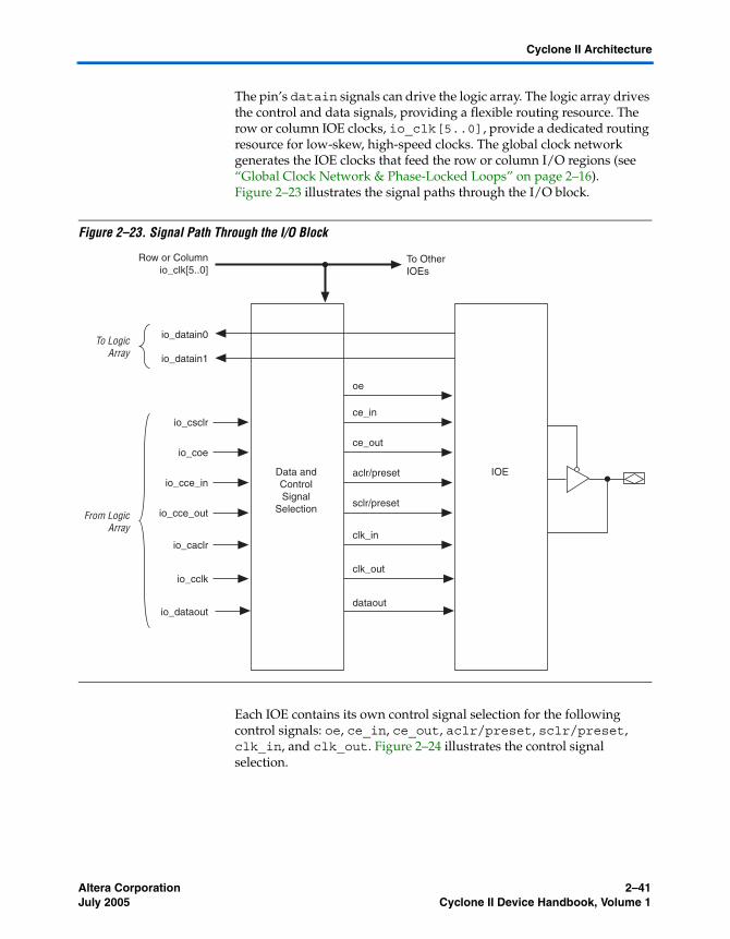
The pin’s datain signals can drive the logic array. The logic array drives the control and data signals, providing a flexible routing resource. The row or column IOE clocks, io_clk[5..0], provide a dedicated routing resource for low-skew, high-speed clocks. The global clock network generates the IOE clocks that feed the row or column I/O regions (see “Global Clock Network & Phase-Locked Loops” on page 2–16). Figure 2–23 illustrates the signal paths through the I/O block.
Figure 2–23. Signal Path Through the I/O Block
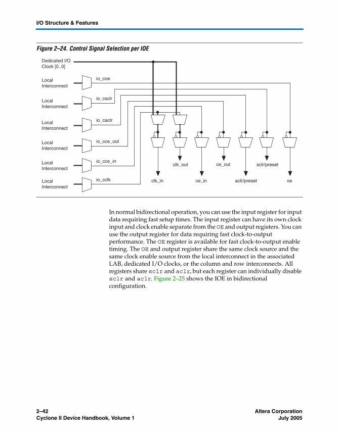
Each IOE contains its own control signal selection for the following control signals: oe, ce_in, ce_out, aclr/preset, sclr/preset, clk_in, and clk_out. Figure 2–24 illustrates the control signal selection.
Row or Columnio_clk[5..0]
io_datain0
io_datain1
io_dataout
io_coe
oe
ce_in
ce_out
io_cce_inaclr/preset
io_cce_outsclr/preset
io_caclrclk_in
io_cclkclk_out
dataout
Data andControlSignal
Selection
IOE
To LogicArray
From LogicArray
To OtherIOEs
io_csclr
Altera Corporation 2–41July 2005 Cyclone II Device Handbook, Volume 1
I/O Structure & Features
Figure 2–24. Control Signal Selection per IOE
In normal bidirectional operation, you can use the input register for input data requiring fast setup times. The input register can have its own clock input and clock enable separate from the OE and output registers. You can use the output register for data requiring fast clock-to-output performance. The OE register is available for fast clock-to-output enable timing. The OE and output register share the same clock source and the same clock enable source from the local interconnect in the associated LAB, dedicated I/O clocks, or the column and row interconnects. All registers share sclr and aclr, but each register can individually disable sclr and aclr. Figure 2–25 shows the IOE in bidirectional configuration.
clk_out
ce_inclk_in
ce_out
aclr/preset
sclr/preset
Dedicated I/OClock [5..0]
LocalInterconnect
LocalInterconnect
LocalInterconnect
LocalInterconnect
LocalInterconnect
oe
io_coe
io_caclr
LocalInterconnect
io_csclr
io_cce_out
io_cce_in
io_cclk
2–42 Altera CorporationCyclone II Device Handbook, Volume 1 July 2005
Cyclone II Architecture
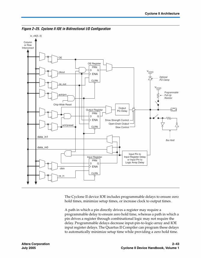
Figure 2–25. Cyclone II IOE in Bidirectional I/O Configuration
The Cyclone II device IOE includes programmable delays to ensure zero hold times, minimize setup times, or increase clock to output times.
A path in which a pin directly drives a register may require a programmable delay to ensure zero hold time, whereas a path in which a pin drives a register through combinational logic may not require the delay. Programmable delays decrease input-pin-to-logic-array and IOE input register delays. The Quartus II Compiler can program these delays to automatically minimize setup time while providing a zero hold time.
Chip-Wide Reset
OE Register
VCCIO
OptionalPCI Clamp
Columnor Row
Interconect
io_clk[5..0]
Input RegisterInput Pin to
Input Register Delayor Input Pin to
Logic Array Delay
Drive Strength Control
Open-Drain Output
Slew Controlsclr/preset
OE
clkout
ce_out
aclr/prn
clkin
ce_in
OutputPin Delay
ProgrammablePull-UpResistor
Bus Hold
PRN
CLRN
D Q
Output Register
PRN
CLRN
D Q
PRN
CLRN
D Q
VCCIO
data_in0
data_in1
ENA
ENA
ENA
Altera Corporation 2–43July 2005 Cyclone II Device Handbook, Volume 1
I/O Structure & Features
Programmable delays can increase the register-to-pin delays for output registers. Table 2–14 shows the programmable delays for Cyclone II devices.
There are two paths in the IOE for an input to reach the logic array. Each of the two paths can have a different delay. This allows you to adjust delays from the pin to internal LE registers that reside in two different areas of the device. You set the two combinational input delays by selecting different delays for two different paths under the Input delay from pin to internal cells logic option in the Quartus II software. However, if the pin uses the input register, one of delays is disregarded because the IOE only has two paths to internal logic. If the input register is used, the IOE uses one input path. The other input path is then available for the combinational path, and only one input delay assignment is applied.
The IOE registers in each I/O block share the same source for clear or preset. You can program preset or clear for each individual IOE, but both features cannot be used simultaneously. You can also program the registers to power up high or low after configuration is complete. If programmed to power up low, an asynchronous clear can control the registers. If programmed to power up high, an asynchronous preset can control the registers. This feature prevents the inadvertent activation of another device’s active-low input upon power up. If one register in an IOE uses a preset or clear signal then all registers in the IOE must use that same signal if they require preset or clear. Additionally a synchronous reset signal is available for the IOE registers.
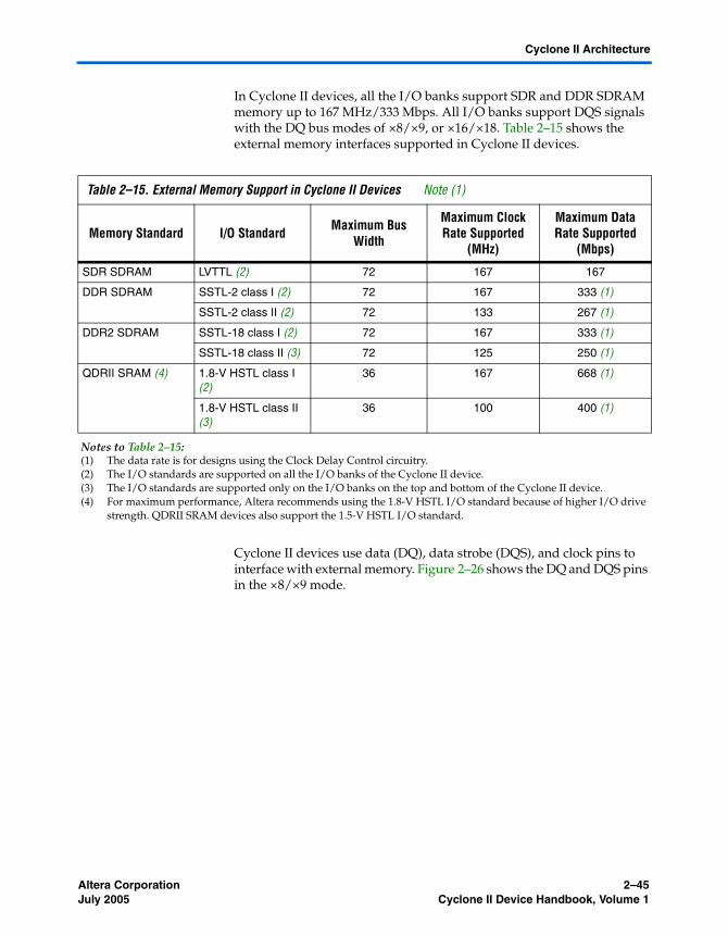
External Memory Interfacing
Cyclone II devices support a broad range of external memory interfaces such as SDR SDRAM, DDR SDRAM, DDR2 SDRAM, and QDRII SRAM external memories. Cyclone II devices feature dedicated high-speed interfaces that transfer data between external memory devices at up to 167 MHz/333 Mbps for DDR and DDR2 SDRAM devices and 167 MHz/667 Mbps for QDRII SRAM devices. The programmable DQS delay chain allows you to fine tune the phase shift for the input clocks or strobes to properly align clock edges as needed to capture data.
Table 2–14. Cyclone II Programmable Delay Chain
Programmable Delays Quartus II Logic Option
Input pin to logic array delay Input delay from pin to internal cells
Input pin to input register delay Input delay from pin to input register
Output pin delay Delay from output register to output pin
2–44 Altera CorporationCyclone II Device Handbook, Volume 1 July 2005
Cyclone II Architecture
In Cyclone II devices, all the I/O banks support SDR and DDR SDRAM memory up to 167 MHz/333 Mbps. All I/O banks support DQS signals with the DQ bus modes of ×8/×9, or ×16/×18. Table 2–15 shows the external memory interfaces supported in Cyclone II devices.
Cyclone II devices use data (DQ), data strobe (DQS), and clock pins to interface with external memory. Figure 2–26 shows the DQ and DQS pins in the ×8/×9 mode.
Table 2–15. External Memory Support in Cyclone II Devices Note (1)
Memory Standard I/O Standard Maximum Bus Width
Maximum Clock Rate Supported
(MHz)
Maximum Data Rate Supported
(Mbps)
SDR SDRAM LVTTL (2) 72 167 167
DDR SDRAM SSTL-2 class I (2) 72 167 333 (1)
SSTL-2 class II (2) 72 133 267 (1)
DDR2 SDRAM SSTL-18 class I (2) 72 167 333 (1)
SSTL-18 class II (3) 72 125 250 (1)
QDRII SRAM (4) 1.8-V HSTL class I (2)
36 167 668 (1)
1.8-V HSTL class II (3)
36 100 400 (1)
Notes to Table 2–15:(1) The data rate is for designs using the Clock Delay Control circuitry.(2) The I/O standards are supported on all the I/O banks of the Cyclone II device.(3) The I/O standards are supported only on the I/O banks on the top and bottom of the Cyclone II device.(4) For maximum performance, Altera recommends using the 1.8-V HSTL I/O standard because of higher I/O drive
strength. QDRII SRAM devices also support the 1.5-V HSTL I/O standard.
Altera Corporation 2–45July 2005 Cyclone II Device Handbook, Volume 1
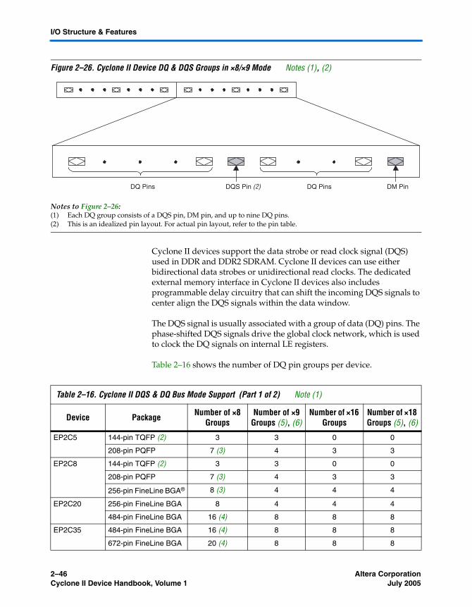
I/O Structure & Features
Figure 2–26. Cyclone II Device DQ & DQS Groups in ×8/×9 Mode Notes (1), (2)
Notes to Figure 2–26:(1) Each DQ group consists of a DQS pin, DM pin, and up to nine DQ pins.(2) This is an idealized pin layout. For actual pin layout, refer to the pin table.
Cyclone II devices support the data strobe or read clock signal (DQS) used in DDR and DDR2 SDRAM. Cyclone II devices can use either bidirectional data strobes or unidirectional read clocks. The dedicated external memory interface in Cyclone II devices also includes programmable delay circuitry that can shift the incoming DQS signals to center align the DQS signals within the data window.
The DQS signal is usually associated with a group of data (DQ) pins. The phase-shifted DQS signals drive the global clock network, which is used to clock the DQ signals on internal LE registers.
Table 2–16 shows the number of DQ pin groups per device.
DQ Pins DQS Pin DM PinDQ Pins(2)
Table 2–16. Cyclone II DQS & DQ Bus Mode Support (Part 1 of 2) Note (1)
Device Package Number of ×8 Groups
Number of ×9 Groups (5), (6)
Number of ×16 Groups
Number of ×18 Groups (5), (6)
EP2C5 144-pin TQFP (2) 3 3 0 0
208-pin PQFP 7 (3) 4 3 3
EP2C8 144-pin TQFP (2) 3 3 0 0
208-pin PQFP 7 (3) 4 3 3
256-pin FineLine BGA® 8 (3) 4 4 4
EP2C20 256-pin FineLine BGA 8 4 4 4
484-pin FineLine BGA 16 (4) 8 8 8
EP2C35 484-pin FineLine BGA 16 (4) 8 8 8
672-pin FineLine BGA 20 (4) 8 8 8
2–46 Altera CorporationCyclone II Device Handbook, Volume 1 July 2005
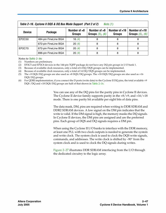
Cyclone II Architecture
You can use any of the DQ pins for the parity pins in Cyclone II devices. The Cyclone II device family supports parity in the ×8/×9, and ×16/×18 mode. There is one parity bit available per eight bits of data pins.
The data mask, DM, pins are required when writing to DDR SDRAM and DDR2 SDRAM devices. A low signal on the DM pin indicates that the write is valid. If the DM signal is high, the memory masks the DQ signals. In Cyclone II devices, the DM pins are assigned and are the preferred pins. Each group of DQS and DQ signals requires a DM pin.
When using the Cyclone II I/O banks to interface with the DDR memory, at least one PLL with two clock outputs is needed to generate the system and write clock. The system clock is used to clock the DQS write signals, commands, and addresses. The write clock is shifted by –90° from the system clock and is used to clock the DQ signals during writes.
Figure 2–27 illustrates DDR SDRAM interfacing from the I/O through the dedicated circuitry to the logic array.
EP2C50 484-pin FineLine BGA 16 (4) 8 8 8
672-pin FineLine BGA 20 (4) 8 8 8
EP2C70 672-pin FineLine BGA 20 (4) 8 8 8
896-pin FineLine BGA 20 (4) 8 8 8
Notes to Table 2–16:(1) Numbers are preliminary.(2) EP2C5 and EP2C8 devices in the 144-pin TQFP package do not have any DQ pin groups in I/O bank 1.(3) Because of available clock resources, only a total of 6 DQ/DQS groups can be implemented.(4) Because of available clock resources, only a total of 14 DQ/DQS groups can be implemented.(5) The ×9 DQS/DQ groups are also used as ×8 DQS/DQ groups. The ×18 DQS/DQ groups are also used as ×16
DQS/DQ groups.(6) For QDRI implementation, if you connect the D ports (write data) to the Cyclone II DQ pins, the total available ×9
DQS /DQ and ×18 DQS/DQ groups are half of that shown in Table 2–16.
Table 2–16. Cyclone II DQS & DQ Bus Mode Support (Part 2 of 2) Note (1)
Device Package Number of ×8 Groups
Number of ×9 Groups (5), (6)
Number of ×16 Groups
Number of ×18 Groups (5), (6)
Altera Corporation 2–47July 2005 Cyclone II Device Handbook, Volume 1
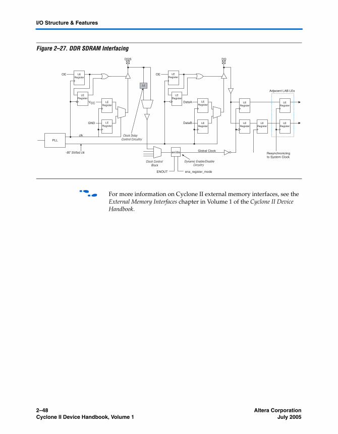
I/O Structure & Features
Figure 2–27. DDR SDRAM Interfacing
f For more information on Cyclone II external memory interfaces, see the External Memory Interfaces chapter in Volume 1 of the Cyclone II Device Handbook.
DQS
OE
VCC
PLL
GND
clk
DQ
OE
DataA
DataB
Resynchronizingto System Clock
Global Clock
Clock DelayControl Circuitry
-90˚ Shifted clk
Adjacent LAB LEs
Clock ControlBlock
LERegister
LERegister
LERegister
LERegister
t
en/dis
Dynamic Enable/DisableCircuitry
ENOUT ena_register_mode
LERegister
LERegister
LERegister
LERegister
LERegister
LERegister
LERegister
LERegister
LERegister
2–48 Altera CorporationCyclone II Device Handbook, Volume 1 July 2005
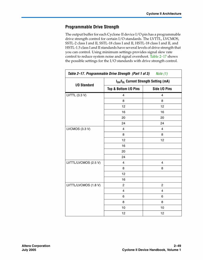
Cyclone II Architecture
Programmable Drive Strength
The output buffer for each Cyclone II device I/O pin has a programmable drive strength control for certain I/O standards. The LVTTL, LVCMOS, SSTL-2 class I and II, SSTL-18 class I and II, HSTL-18 class I and II, and HSTL-1.5 class I and II standards have several levels of drive strength that you can control. Using minimum settings provides signal slew rate control to reduce system noise and signal overshoot. Table 2–17 shows the possible settings for the I/O standards with drive strength control.
Table 2–17. Programmable Drive Strength (Part 1 of 3) Note (1)
I/O StandardIOH/IOL Current Strength Setting (mA)
Top & Bottom I/O Pins Side I/O Pins
LVTTL (3.3 V) 4 4
8 8
12 12
16 16
20 20
24 24
LVCMOS (3.3 V) 4 4
8 8
12 12
16
20
24
LVTTL/LVCMOS (2.5 V) 4 4
8 8
12
16
LVTTL/LVCMOS (1.8 V) 2 2
4 4
6 6
8 8
10 10
12 12
Altera Corporation 2–49July 2005 Cyclone II Device Handbook, Volume 1
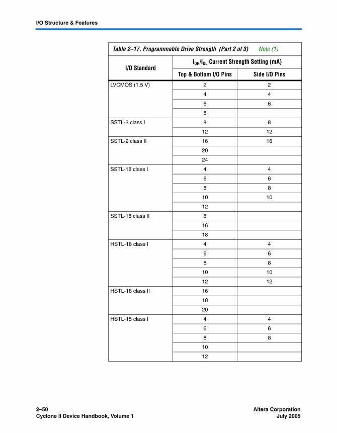
I/O Structure & Features
LVCMOS (1.5 V) 2 2
4 4
6 6
8
SSTL-2 class I 8 8
12 12
SSTL-2 class II 16 16
20
24
SSTL-18 class I 4 4
6 6
8 8
10 10
12
SSTL-18 class II 8
16
18
HSTL-18 class I 4 4
6 6
8 8
10 10
12 12
HSTL-18 class II 16
18
20
HSTL-15 class I 4 4
6 6
8 8
10
12
Table 2–17. Programmable Drive Strength (Part 2 of 3) Note (1)
I/O StandardIOH/IOL Current Strength Setting (mA)
Top & Bottom I/O Pins Side I/O Pins
2–50 Altera CorporationCyclone II Device Handbook, Volume 1 July 2005

Cyclone II Architecture
Open-Drain Output
Cyclone II devices provide an optional open-drain (equivalent to an open-collector) output for each I/O pin. This open-drain output enables the device to provide system-level control signals (that is, interrupt and write-enable signals) that can be asserted by any of several devices.
Slew Rate Control
Slew rate control is performed by using programmable output drive strength.
Bus Hold
Each Cyclone II device user I/O pin provides an optional bus-hold feature. The bus-hold circuitry can hold the signal on an I/O pin at its last-driven state. Since the bus-hold feature holds the last-driven state of the pin until the next input signal is present, an external pull-up or pull-down resistor is not necessary to hold a signal level when the bus is tri-stated.
The bus-hold circuitry also pulls undriven pins away from the input threshold voltage where noise can cause unintended high-frequency switching. You can select this feature individually for each I/O pin. The bus-hold output drives no higher than VCCIO to prevent overdriving signals.
1 If the bus-hold feature is enabled, the device cannot use the programmable pull-up option. Disable the bus-hold feature when the I/O pin is configured for differential signals. Bus hold circuitry is not available on the dedicated clock pins.
The bus-hold circuitry is only active after configuration. When going into user mode, the bus-hold circuit captures the value on the pin present at the end of configuration.
HSTL-15 class II 16
Note to Table 2–17:(1) The default current in the Quartus II software is the maximum setting for each
I/O standard.
Table 2–17. Programmable Drive Strength (Part 3 of 3) Note (1)
I/O StandardIOH/IOL Current Strength Setting (mA)
Top & Bottom I/O Pins Side I/O Pins
Altera Corporation 2–51July 2005 Cyclone II Device Handbook, Volume 1
I/O Structure & Features
The bus-hold circuitry uses a resistor with a nominal resistance (RBH) of approximately 7 kΩ to pull the signal level to the last-driven state. Refer to the DC Characteristics & Timing Specifications chapter in Volume 1 of the Cyclone II Device Handbook for the specific sustaining current for each VCCIO voltage level driven through the resistor and overdrive current used to identify the next driven input level.
Programmable Pull-Up Resistor
Each Cyclone II device I/O pin provides an optional programmable pull-up resistor during user mode. If you enable this feature for an I/O pin, the pull-up resistor (typically 25 kΩ) holds the output to the VCCIO level of the output pin’s bank.
1 If the programmable pull-up is enabled, the device cannot use the bus-hold feature. The programmable pull-up resistors are not supported on the dedicated configuration, JTAG, and dedicated clock pins.
2–52 Altera CorporationCyclone II Device Handbook, Volume 1 July 2005
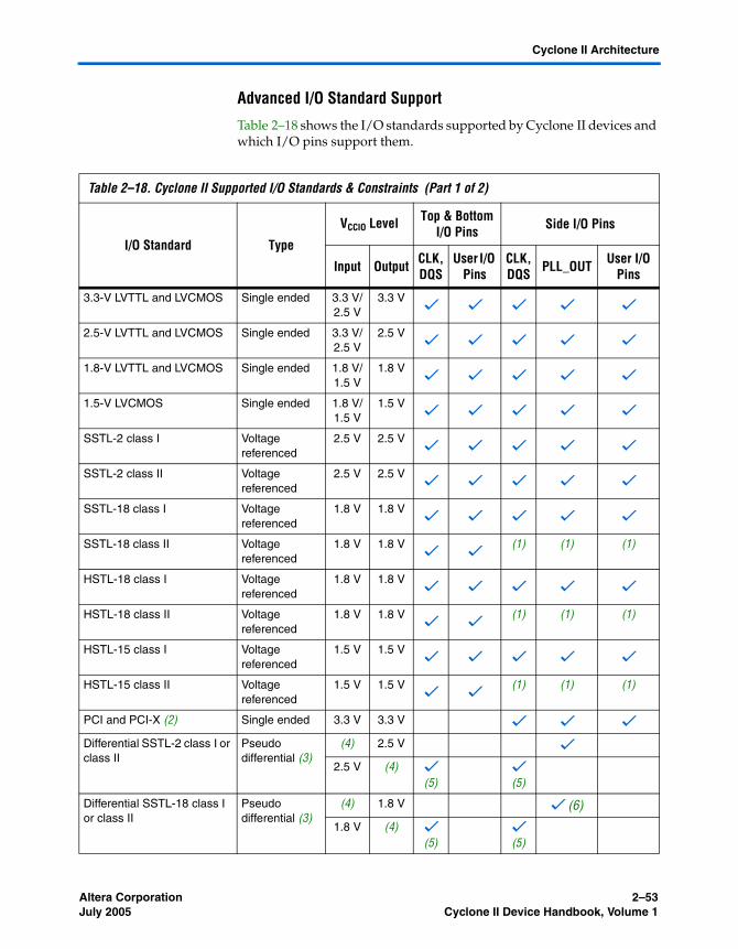
Cyclone II Architecture
Advanced I/O Standard Support
Table 2–18 shows the I/O standards supported by Cyclone II devices and which I/O pins support them.
Table 2–18. Cyclone II Supported I/O Standards & Constraints (Part 1 of 2)
I/O Standard Type
VCCIO Level Top & Bottom I/O Pins Side I/O Pins
Input Output CLK, DQS
User I/O Pins
CLK, DQS PLL_OUT User I/O
Pins
3.3-V LVTTL and LVCMOS Single ended 3.3 V/2.5 V
3.3 Vv v v v v
2.5-V LVTTL and LVCMOS Single ended 3.3 V/2.5 V
2.5 Vv v v v v
1.8-V LVTTL and LVCMOS Single ended 1.8 V/1.5 V
1.8 Vv v v v v
1.5-V LVCMOS Single ended 1.8 V/1.5 V
1.5 Vv v v v v
SSTL-2 class I Voltage referenced
2.5 V 2.5 Vv v v v v
SSTL-2 class II Voltage referenced
2.5 V 2.5 Vv v v v v
SSTL-18 class I Voltage referenced
1.8 V 1.8 Vv v v v v
SSTL-18 class II Voltage referenced
1.8 V 1.8 Vv v
(1) (1) (1)
HSTL-18 class I Voltage referenced
1.8 V 1.8 Vv v v v v
HSTL-18 class II Voltage referenced
1.8 V 1.8 Vv v
(1) (1) (1)
HSTL-15 class I Voltage referenced
1.5 V 1.5 Vv v v v v
HSTL-15 class II Voltage referenced
1.5 V 1.5 Vv v
(1) (1) (1)
PCI and PCI-X (2) Single ended 3.3 V 3.3 V v v v
Differential SSTL-2 class I or class II
Pseudo differential (3)
(4) 2.5 V v
2.5 V (4) v (5)
v (5)
Differential SSTL-18 class I or class II
Pseudo differential (3)
(4) 1.8 V v (6)
1.8 V (4) v (5)
v (5)
Altera Corporation 2–53July 2005 Cyclone II Device Handbook, Volume 1
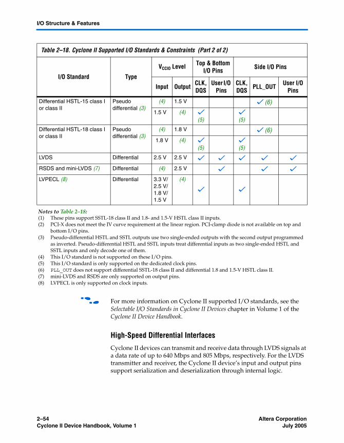
I/O Structure & Features
f For more information on Cyclone II supported I/O standards, see the Selectable I/O Standards in Cyclone II Devices chapter in Volume 1 of the Cyclone II Device Handbook.
High-Speed Differential Interfaces
Cyclone II devices can transmit and receive data through LVDS signals at a data rate of up to 640 Mbps and 805 Mbps, respectively. For the LVDS transmitter and receiver, the Cyclone II device’s input and output pins support serialization and deserialization through internal logic.
Differential HSTL-15 class I or class II
Pseudo differential (3)
(4) 1.5 V v (6)
1.5 V (4) v (5)
v (5)
Differential HSTL-18 class I or class II
Pseudo differential (3)
(4) 1.8 V v (6)
1.8 V (4) v (5)
v (5)
LVDS Differential 2.5 V 2.5 V v v v v v
RSDS and mini-LVDS (7) Differential (4) 2.5 V v v v
LVPECL (8) Differential 3.3 V/2.5 V/1.8 V/1.5 V
(4)
v v
Notes to Table 2–18:(1) These pins support SSTL-18 class II and 1.8- and 1.5-V HSTL class II inputs.(2) PCI-X does not meet the IV curve requirement at the linear region. PCI-clamp diode is not available on top and
bottom I/O pins.(3) Pseudo-differential HSTL and SSTL outputs use two single-ended outputs with the second output programmed
as inverted. Pseudo-differential HSTL and SSTL inputs treat differential inputs as two single-ended HSTL and SSTL inputs and only decode one of them.
(4) This I/O standard is not supported on these I/O pins.(5) This I/O standard is only supported on the dedicated clock pins.(6) PLL_OUT does not support differential SSTL-18 class II and differential 1.8 and 1.5-V HSTL class II.(7) mini-LVDS and RSDS are only supported on output pins.(8) LVPECL is only supported on clock inputs.
Table 2–18. Cyclone II Supported I/O Standards & Constraints (Part 2 of 2)
I/O Standard Type
VCCIO Level Top & Bottom I/O Pins Side I/O Pins
Input Output CLK, DQS
User I/O Pins
CLK, DQS PLL_OUT User I/O
Pins
2–54 Altera CorporationCyclone II Device Handbook, Volume 1 July 2005
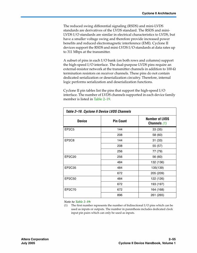
Cyclone II Architecture
The reduced swing differential signaling (RSDS) and mini-LVDS standards are derivatives of the LVDS standard. The RSDS and mini-LVDS I/O standards are similar in electrical characteristics to LVDS, but have a smaller voltage swing and therefore provide increased power benefits and reduced electromagnetic interference (EMI). Cyclone II devices support the RSDS and mini-LVDS I/O standards at data rates up to 311 Mbps at the transmitter.
A subset of pins in each I/O bank (on both rows and columns) support the high-speed I/O interface. The dual-purpose LVDS pins require an external-resistor network at the transmitter channels in addition to 100-Ω termination resistors on receiver channels. These pins do not contain dedicated serialization or deserialization circuitry. Therefore, internal logic performs serialization and deserialization functions.
Cyclone II pin tables list the pins that support the high-speed I/O interface. The number of LVDS channels supported in each device family member is listed in Table 2–19.
Table 2–19. Cyclone II Device LVDS Channels
Device Pin Count Number of LVDS Channels (1)
EP2C5 144 33 (35)
208 58 (60)
EP2C8 144 31 (33)
208 55 (57)
256 77 (79)
EP2C20 256 56 (60)
484 132 (136)
EP2C35 484 135(139)
672 205 (209)
EP2C50 484 122 (126)
672 193 (197)
EP2C70 672 164 (168)
896 261 (265)
Note to Table 2–19:(1) The first number represents the number of bidirectional I/O pins which can be
used as inputs or outputs. The number in parenthesis includes dedicated clock input pin pairs which can only be used as inputs.
Altera Corporation 2–55July 2005 Cyclone II Device Handbook, Volume 1
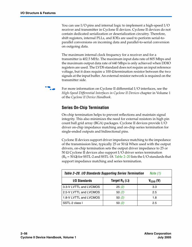
I/O Structure & Features
You can use I/O pins and internal logic to implement a high-speed I/O receiver and transmitter in Cyclone II devices. Cyclone II devices do not contain dedicated serialization or deserialization circuitry. Therefore, shift registers, internal PLLs, and IOEs are used to perform serial-to-parallel conversions on incoming data and parallel-to-serial conversion on outgoing data.
The maximum internal clock frequency for a receiver and for a transmitter is 402.5 MHz. The maximum input data rate of 805 Mbps and the maximum output data rate of 640 Mbps is only achieved when DDIO registers are used. The LVDS standard does not require an input reference voltage, but it does require a 100-Ω termination resistor between the two signals at the input buffer. An external resistor network is required on the transmitter side.
f For more information on Cyclone II differential I/O interfaces, see the High-Speed Differential Interfaces in Cyclone II Devices chapter in Volume 1 of the Cyclone II Device Handbook.
Series On-Chip Termination
On-chip termination helps to prevent reflections and maintain signal integrity. This also minimizes the need for external resistors in high pin count ball grid array (BGA) packages. Cyclone II devices provide I/O driver on-chip impedance matching and on-chip series termination for single-ended outputs and bidirectional pins.
Cyclone II devices support driver impedance matching to the impedance of the transmission line, typically 25 or 50 Ω. When used with the output drivers, on-chip termination sets the output driver impedance to 25 or 50 Ω. Cyclone II devices also support I/O driver series termination (RS = 50 Ω) for SSTL-2 and SSTL-18. Table 2–20 lists the I/O standards that support impedance matching and series termination.
Table 2–20. I/O Standards Supporting Series Termination Note (1)
I/O Standards Target RS (Ω) VCCIO (V)
3.3-V LVTTL and LVCMOS 25 (2) 3.3
2.5-V LVTTL and LVCMOS 50 (2) 2.5
1.8-V LVTTL and LVCMOS 50 (2) 1.8
SSTL-2 class I 50 (2) 2.5
2–56 Altera CorporationCyclone II Device Handbook, Volume 1 July 2005
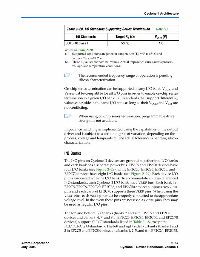
Cyclone II Architecture
1 The recommended frequency range of operation is pending silicon characterization.
On-chip series termination can be supported on any I/O bank. VCCIO and VREF must be compatible for all I/O pins in order to enable on-chip series termination in a given I/O bank. I/O standards that support different RS values can reside in the same I/O bank as long as their VCCIO and VREF are not conflicting.
1 When using on-chip series termination, programmable drive strength is not available.
Impedance matching is implemented using the capabilities of the output driver and is subject to a certain degree of variation, depending on the process, voltage and temperature. The actual tolerance is pending silicon characterization.
I/O Banks
The I/O pins on Cyclone II devices are grouped together into I/O banks and each bank has a separate power bus. EP2C5 and EP2C8 devices have four I/O banks (see Figure 2–28), while EP2C20, EP2C35, EP2C50, and EP2C70 devices have eight I/O banks (see Figure 2–29). Each device I/O pin is associated with one I/O bank. To accommodate voltage-referenced I/O standards, each Cyclone II I/O bank has a VREF bus. Each bank in EP2C5, EP2C8, EP2C20, EP2C35, and EP2C50 devices supports two VREF pins and each bank of EP2C70 supports three VREF pins. When using the VREF pins, each VREF pin must be properly connected to the appropriate voltage level. In the event these pins are not used as VREF pins, they may be used as regular I/O pins.
The top and bottom I/O banks (banks 2 and 4 in EP2C5 and EP2C8 devices and banks 3, 4, 7, and 8 in EP2C20, EP2C35, EP2C50, and EP2C70 devices) support all I/O standards listed in Table 2–18, except the PCI/PCI-X I/O standards. The left and right side I/O banks (banks 1 and 3 in EP2C5 and EP2C8 devices and banks 1, 2, 5, and 6 in EP2C20, EP2C35,
SSTL-18 class I 50 (2) 1.8
Notes to Table 2–20:(1) Supported conditions are junction temperature (TJ) = 0° to 85° C and
VCCIO = VCCIO ±50 mV.(2) These RS values are nominal values. Actual impedance varies across process,
voltage, and temperature conditions.
Table 2–20. I/O Standards Supporting Series Termination Note (1)
I/O Standards Target RS (Ω) VCCIO (V)
Altera Corporation 2–57July 2005 Cyclone II Device Handbook, Volume 1
I/O Structure & Features
EP2C50, and EP2C70 devices) support I/O standards listed in Table 2–18, except SSTL-18 class II, HSTL-18 class II, and HSTL-15 class II I/O standards. See Table 2–18 for a complete list of supported I/O standards.
The top and bottom I/O banks (banks 2 and 4 in EP2C5 and EP2C8 devices and banks 3, 4, 7, and 8 in EP2C20, EP2C35, EP2C50, and EP2C70 devices) support DDR2 memory up to 167 MHz/333 Mbps and QDR memory up to 167 MHz/668 Mbps. The left and right side I/O banks (1 and 3 of EP2C5 and EP2C8 devices and 1, 2, 5, and 6 of EP2C20, EP2C35, EP2C50, and EP2C70 devices) only support SDR and DDR SDRAM interfaces. All the I/O banks of the Cyclone II devices support SDR memory up to 167 MHz/167 Mbps and DDR memory up to 167 MHz/333 Mbps.
2–58 Altera CorporationCyclone II Device Handbook, Volume 1 July 2005
Cyclone II Architecture
Figure 2–28. EP2C5 & EP2C8 I/O Banks Notes (1), (2)
Notes to Figure 2–28:(1) This is a top view of the silicon die.(2) This is a graphic representation only. Refer to the pin list and the Quartus II software for exact pin locations.(3) The LVPECL I/O standard is only supported on clock input pins. This I/O standard is not supported on output
pins.(4) The differential SSTL-18 and SSTL-2 I/O standards are only supported on clock input pins and PLL output clock
pins.(5) The differential 1.8-V and 1.5-V HSTL I/O standards are only supported on clock input pins and PLL output clock
pins.
I/O Bank 2
I/O Bank 3
I/O Bank 4
I/O Bank 1
All I/O Banks Support■ 3.3-V LVTTL/LVCMOS ■ 2.5-V LVTTL/LVCMOS■ 1.8-V LVTTL/LVCMOS■ 1.5-V LVCMOS■ LVDS■ RSDS■ mini-LVDS■ LVPECL (3)■ SSTL-2 Class I and II■ SSTL-18 Class I■ HSTL-18 Class I■ HSTL-15 Class I■ Differential SSTL-2 (4)■ Differential SSTL-18 (4)■ Differential HSTL-18 (5)■ Differential HSTL-15 (5)
I/O Bank 3Also Supports the 3.3-V PCI & PCI-XI/O Standards
I/O Bank 1Also Supports the3.3-V PCI & PCI-X
I/O Standards
IndividualPower Bus
I/O Bank 2 Also Supportsthe SSTL-18 Class II,
HSTL-18 Class II, & HSTL-15Class II I/O Standards
I/O Bank 4 Also Supportsthe SSTL-18 Class II,
HSTL-18 Class II, & HSTL-15Class II I/O Standards
Altera Corporation 2–59July 2005 Cyclone II Device Handbook, Volume 1
I/O Structure & Features
Figure 2–29. EP2C20, EP2C35, EP2C50 & EP2C70 I/O Banks Notes (1), (2)
Notes to Figure 2–29:(1) This is a top view of the silicon die.(2) This is a graphic representation only. Refer to the pin list and the Quartus II software for exact pin locations.(3) The LVPECL I/O standard is only supported on clock input pins. This I/O standard is not supported on output
pins.(4) The differential SSTL-18 and SSTL-2 I/O standards are only supported on clock input pins and PLL output clock
pins.(5) The differential 1.8-V and 1.5-V HSTL I/O standards are only supported on clock input pins and PLL output clock
pins.
Each I/O bank has its own VCCIO pins. A single device can support 1.5-V, 1.8-V, 2.5-V, and 3.3-V interfaces; each individual bank can support a different standard with different I/O voltages. Each bank also has dual-purpose VREF pins to support any one of the voltage-referenced
I/O Bank 2
Regular I/O BlockBank 8
Regular I/O BlockBank 7
I/O Bank 3 I/O Bank 4
I/O Bank 1
I/O Bank 5
I/O Bank 6
IndividualPower Bus
All I/O Banks Support■ 3.3-V LVTTL/LVCMOS ■ 2.5-V LVTTL/LVCMOS■ 1.8-V LVTTL/LVCMOS■ 1.5-V LVCMOS■ LVDS■ RSDS■ mini-LVDS■ LVPECL (3)■ SSTL-2 Class I and II■ SSTL-18 Class I■ HSTL-18 Class I■ HSTL-15 Class I■ Differential SSTL-2 (4)■ Differential SSTL-18 (4)■ Differential HSTL-18 (5)■ Differential HSTL-15 (5)
I/O Banks 3 & 4 Also Supportthe SSTL-18 Class II,
HSTL-18 Class II, & HSTL-15Class II I/O Standards
I/O Banks 7 & 8 Also Supportthe SSTL-18 Class II,
HSTL-18 Class II, & HSTL-15Class II I/O Standards
I/O Banks 5 & 6 AlsoSupport the 3.3-V PCI& PCI-X I/O Standards
I/O Banks 1 & 2 AlsoSupport the 3.3-V PCI& PCI-X I/O Standards
2–60 Altera CorporationCyclone II Device Handbook, Volume 1 July 2005
Cyclone II Architecture
standards (e.g., SSTL-2) independently. If an I/O bank does not use voltage-referenced standards, the VREF pins are available as user I/O pins.
Each I/O bank can support multiple standards with the same VCCIO for input and output pins. For example, when VCCIO is 3.3-V, a bank can support LVTTL, LVCMOS, and 3.3-V PCI for inputs and outputs. Voltage-referenced standards can be supported in an I/O bank using any number of single-ended or differential standards as long as they use the same VREF and a compatible VCCIO value.
MultiVolt I/O Interface
The Cyclone II architecture supports the MultiVolt I/O interface feature, which allows Cyclone II devices in all packages to interface with systems of different supply voltages. Cyclone II devices have one set of VCC pins (VCCINT) that power the internal device logic array and input buffers that use the LVPECL, LVDS, HSTL, or SSTL I/O standards. Cyclone II devices also have four or eight sets of VCC pins (VCCIO) that power the I/O output drivers and input buffers that use the LVTTL, LVCMOS, or PCI I/O standards.
The Cyclone II VCCINT pins must always be connected to a 1.2-V power supply. If the VCCINT level is 1.2 V, then input pins are 1.5-V, 1.8-V, 2.5-V, and 3.3-V tolerant. The VCCIO pins can be connected to either a 1.5-V, 1.8-V, 2.5-V, or 3.3-V power supply, depending on the output requirements. The output levels are compatible with systems of the same voltage as the power supply (i.e., when VCCIO pins are connected to a 1.5-V power supply, the output levels are compatible with 1.5-V systems). When VCCIO pins are connected to a 3.3-V power supply, the output high is 3.3-V and is compatible with 3.3-V systems. Table 2–21 summarizes Cyclone II MultiVolt I/O support.
Table 2–21. Cyclone II MultiVolt I/O Support (Part 1 of 2) Note (1)
VCCIO (V)Input Signal Output Signal
1.5 V 1.8 V 2.5 V 3.3 V 1.5 V 1.8 V 2.5 V 3.3 V
1.5 v v v (2) v (2) v
1.8 v (4) v v (2) v (2) v (3) v
2.5 v v v (5) v (5) v
Altera Corporation 2–61July 2005 Cyclone II Device Handbook, Volume 1
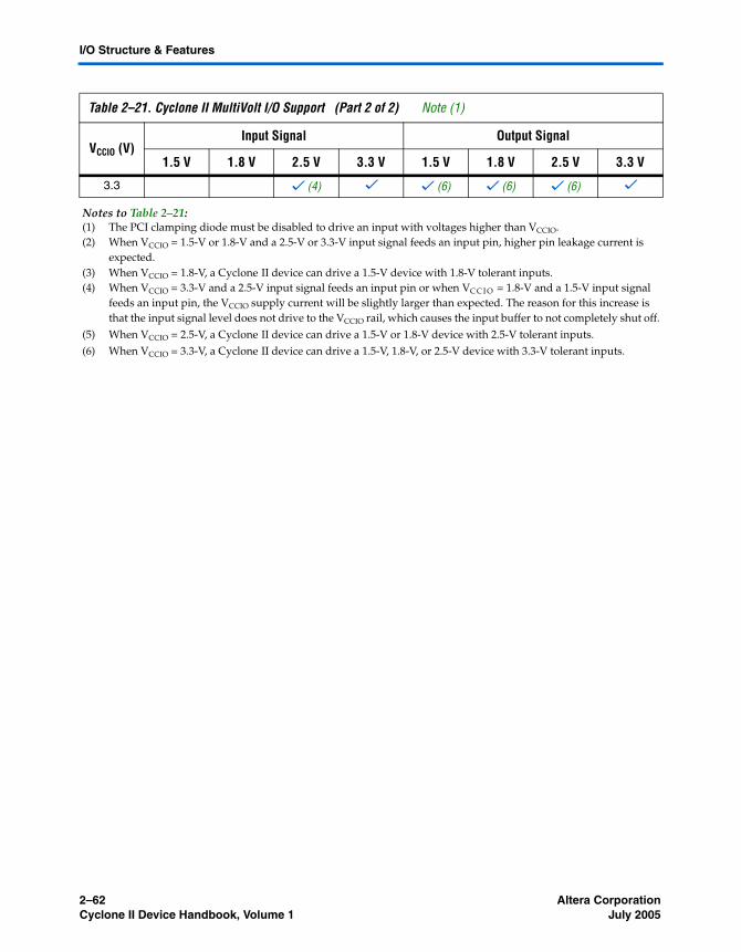
I/O Structure & Features
3.3 v (4) v v (6) v (6) v (6) v
Notes to Table 2–21:(1) The PCI clamping diode must be disabled to drive an input with voltages higher than VCCIO.(2) When VCCIO = 1.5-V or 1.8-V and a 2.5-V or 3.3-V input signal feeds an input pin, higher pin leakage current is
expected.(3) When VCCIO = 1.8-V, a Cyclone II device can drive a 1.5-V device with 1.8-V tolerant inputs.(4) When VCCIO = 3.3-V and a 2.5-V input signal feeds an input pin or when VC C I O = 1.8-V and a 1.5-V input signal
feeds an input pin, the VCCIO supply current will be slightly larger than expected. The reason for this increase is that the input signal level does not drive to the VCCIO rail, which causes the input buffer to not completely shut off.
(5) When VCCIO = 2.5-V, a Cyclone II device can drive a 1.5-V or 1.8-V device with 2.5-V tolerant inputs.(6) When VCCIO = 3.3-V, a Cyclone II device can drive a 1.5-V, 1.8-V, or 2.5-V device with 3.3-V tolerant inputs.
Table 2–21. Cyclone II MultiVolt I/O Support (Part 2 of 2) Note (1)
VCCIO (V)Input Signal Output Signal
1.5 V 1.8 V 2.5 V 3.3 V 1.5 V 1.8 V 2.5 V 3.3 V
2–62 Altera CorporationCyclone II Device Handbook, Volume 1 July 2005
Altera Corporation July 2005
CII51003-2.0
3. Configuration & Testing
IEEE Std. 1149.1 (JTAG) Boundary Scan Support
All Cyclone™ II devices provide JTAG BST circuitry that complies with the IEEE Std. 1149.1. JTAG boundary-scan testing can be performed either before or after, but not during configuration. Cyclone II devices can also use the JTAG port for configuration with the Quartus® II software or hardware using either Jam Files (.jam) or Jam Byte-Code Files (.jbc).
Cyclone II devices support IOE I/O standard reconfiguration through the JTAG BST chain. The JTAG chain can update the I/O standard for all input and output pins any time before or during user mode through the CONFIG_IO instruction. You can use this capability for JTAG testing before configuration when some of the Cyclone II pins drive or receive from other devices on the board using voltage-referenced standards. Since the Cyclone II device might not be configured before JTAG testing, the I/O pins may not be configured for appropriate electrical standards for chip-to-chip communication. Programming the I/O standards via JTAG allows you to fully test I/O connections to other devices.
f For information on I/O reconfiguration, see MorphIO: An I/O Reconfiguration Solution for Altera Devices White Paper.
A device operating in JTAG mode uses four required pins: TDI, TDO, TMS, and TCK. The TCK pin has an internal weak pull-down resister, while the TDI and TMS pins have weak internal pull-up resistors. The TDO output pin and all JTAG input pin voltage is determined by the VCCIO of the bank where it resides. The bank VCCIO selects whether the JTAG inputs are 1.5-, 1.8-, 2.5-, or 3.3-V compatible.
3–1Preliminary
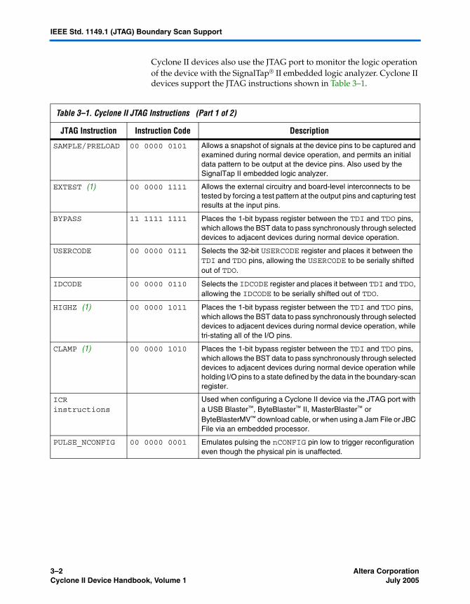
IEEE Std. 1149.1 (JTAG) Boundary Scan Support
Cyclone II devices also use the JTAG port to monitor the logic operation of the device with the SignalTap® II embedded logic analyzer. Cyclone II devices support the JTAG instructions shown in Table 3–1.
Table 3–1. Cyclone II JTAG Instructions (Part 1 of 2)
JTAG Instruction Instruction Code Description
SAMPLE/PRELOAD 00 0000 0101 Allows a snapshot of signals at the device pins to be captured and examined during normal device operation, and permits an initial data pattern to be output at the device pins. Also used by the SignalTap II embedded logic analyzer.
EXTEST (1) 00 0000 1111 Allows the external circuitry and board-level interconnects to be tested by forcing a test pattern at the output pins and capturing test results at the input pins.
BYPASS 11 1111 1111 Places the 1-bit bypass register between the TDI and TDO pins, which allows the BST data to pass synchronously through selected devices to adjacent devices during normal device operation.
USERCODE 00 0000 0111 Selects the 32-bit USERCODE register and places it between the TDI and TDO pins, allowing the USERCODE to be serially shifted out of TDO.
IDCODE 00 0000 0110 Selects the IDCODE register and places it between TDI and TDO, allowing the IDCODE to be serially shifted out of TDO.
HIGHZ (1) 00 0000 1011 Places the 1-bit bypass register between the TDI and TDO pins, which allows the BST data to pass synchronously through selected devices to adjacent devices during normal device operation, while tri-stating all of the I/O pins.
CLAMP (1) 00 0000 1010 Places the 1-bit bypass register between the TDI and TDO pins, which allows the BST data to pass synchronously through selected devices to adjacent devices during normal device operation while holding I/O pins to a state defined by the data in the boundary-scan register.
ICR instructions
Used when configuring a Cyclone II device via the JTAG port with a USB Blaster™, ByteBlaster™ II, MasterBlaster™ or ByteBlasterMV™ download cable, or when using a Jam File or JBC File via an embedded processor.
PULSE_NCONFIG 00 0000 0001 Emulates pulsing the nCONFIG pin low to trigger reconfiguration even though the physical pin is unaffected.
3–2 Altera CorporationCyclone II Device Handbook, Volume 1 July 2005
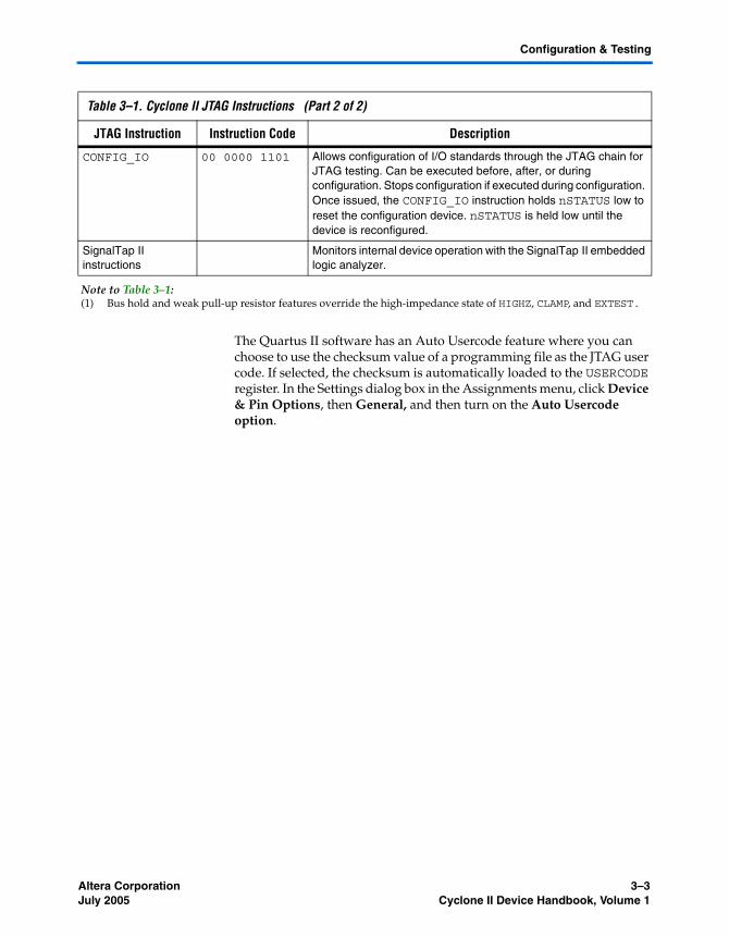
Configuration & Testing
The Quartus II software has an Auto Usercode feature where you can choose to use the checksum value of a programming file as the JTAG user code. If selected, the checksum is automatically loaded to the USERCODE register. In the Settings dialog box in the Assignments menu, click Device & Pin Options, then General, and then turn on the Auto Usercode option.
CONFIG_IO 00 0000 1101 Allows configuration of I/O standards through the JTAG chain for JTAG testing. Can be executed before, after, or during configuration. Stops configuration if executed during configuration. Once issued, the CONFIG_IO instruction holds nSTATUS low to reset the configuration device. nSTATUS is held low until the device is reconfigured.
SignalTap II instructions
Monitors internal device operation with the SignalTap II embedded logic analyzer.
Note to Table 3–1:(1) Bus hold and weak pull-up resistor features override the high-impedance state of HIGHZ, CLAMP, and EXTEST.
Table 3–1. Cyclone II JTAG Instructions (Part 2 of 2)
JTAG Instruction Instruction Code Description
Altera Corporation 3–3July 2005 Cyclone II Device Handbook, Volume 1
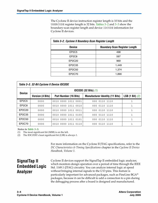
SignalTap II Embedded Logic Analyzer
The Cyclone II device instruction register length is 10 bits and the USERCODE register length is 32 bits. Tables 3–2 and 3–3 show the boundary-scan register length and device IDCODE information for Cyclone II devices.
For more information on the Cyclone II JTAG specifications, refer to the DC Characteristics & Timing Specifications chapter in the Cyclone II Device Handbook, Volume 1.
SignalTap II Embedded Logic Analyzer
Cyclone II devices support the SignalTap II embedded logic analyzer, which monitors design operation over a period of time through the IEEE Std. 1149.1 (JTAG) circuitry. You can analyze internal logic at speed without bringing internal signals to the I/O pins. This feature is particularly important for advanced packages, such as FineLine BGA® packages, because it can be difficult to add a connection to a pin during the debugging process after a board is designed and manufactured.
Table 3–2. Cyclone II Boundary-Scan Register Length
Device Boundary-Scan Register Length
EP2C5 498
EP2C8 597
EP2C20 969
EP2C35 1,449
EP2C50 1,374
EP2C70 1,890
Table 3–3. 32-Bit Cyclone II Device IDCODE
DeviceIDCODE (32 Bits) (1)
Version (4 Bits) Part Number (16 Bits) Manufacturer Identity (11 Bits) LSB (1 Bit) (2)
EP2C5 0000 0010 0000 1011 0001 000 0110 1110 1
EP2C8 0000 0010 0000 1011 0010 000 0110 1110 1
EP2C20 0000 0010 0000 1011 0011 000 0110 1110 1
EP2C35 0000 0010 0000 1011 0100 000 0110 1110 1
EP2C50 0000 0010 0000 1011 0101 000 0110 1110 1
EP2C70 0000 0010 0000 1011 0110 000 0110 1110 1
Notes to Table 3–3:(1) The most significant bit (MSB) is on the left.(2) The IDCODE’s least significant bit (LSB) is always 1.
3–4 Altera CorporationCyclone II Device Handbook, Volume 1 July 2005
Configuration & Testing
f For more information on the SignalTap II, see the Signal Tap chapter of the Quartus II Handbook, Volume 3.
Configuration The logic, circuitry, and interconnects in the Cyclone II architecture are configured with CMOS SRAM elements. Altera FPGA devices are reconfigurable and every device is tested with a high coverage production test program so you do not have to perform fault testing and can instead focus on simulation and design verification.
Cyclone II devices are configured at system power-up with data stored in an Altera configuration device or provided by a system controller. The Cyclone II device’s optimized interface allows the device to act as controller in an active serial configuration scheme with EPCS serial configuration devices. The serial configuration device can be programmed via SRunner, the ByteBlaster II or USB Blaster download cable, the Altera Programming Unit (APU), or third-party programmers.
In addition to EPCS serial configuration devices, Altera offers in-system programmability (ISP)-capable configuration devices that can configure Cyclone II devices via a serial data stream using the Passive serial (PS) configuration mode. The PS interface also enables microprocessors to treat Cyclone II devices as memory and configure them by writing to a virtual memory location, simplifying reconfiguration. After a Cyclone II device has been configured, it can be reconfigured in-circuit by resetting the device and loading new configuration data. Real-time changes can be made during system operation, enabling innovative reconfigurable applications.
Operating Modes
The Cyclone II architecture uses SRAM configuration elements that require configuration data to be loaded each time the circuit powers up. The process of physically loading the SRAM data into the device is called configuration. During initialization, which occurs immediately after configuration, the device resets registers, enables I/O pins, and begins to operate as a logic device. Together, the configuration and initialization processes are called command mode. Normal device operation is called user mode.
SRAM configuration elements allow Cyclone II devices to be reconfigured in-circuit by loading new configuration data into the device. With real-time reconfiguration, the device is forced into command mode with the nCONFIG pin. The configuration process loads different configuration data, reinitializes the device, and resumes user-mode operation. You can perform in-field upgrades by distributing new configuration files within the system or remotely.
Altera Corporation 3–5July 2005 Cyclone II Device Handbook, Volume 1
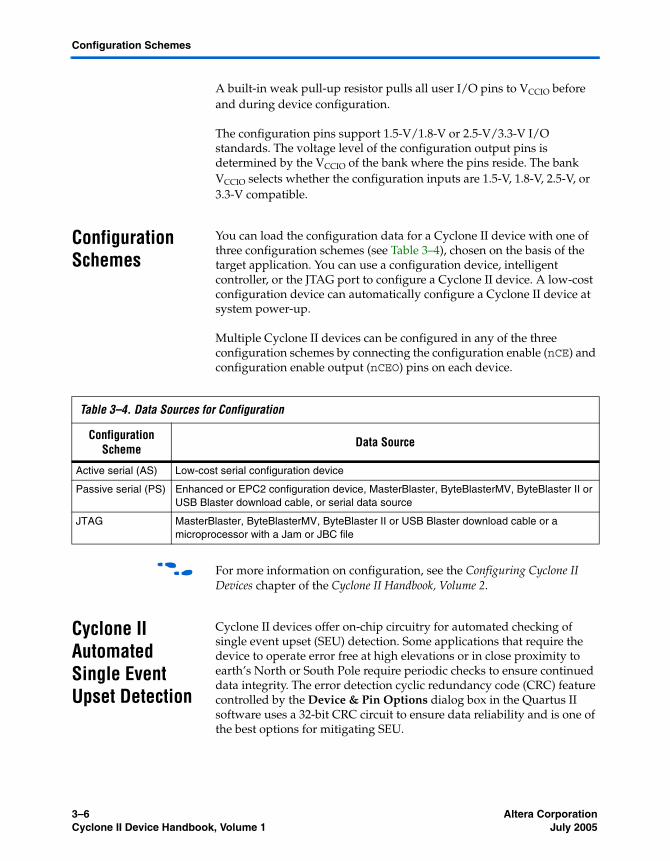
Configuration Schemes
A built-in weak pull-up resistor pulls all user I/O pins to VCCIO before and during device configuration.
The configuration pins support 1.5-V/1.8-V or 2.5-V/3.3-V I/O standards. The voltage level of the configuration output pins is determined by the VCCIO of the bank where the pins reside. The bank VCCIO selects whether the configuration inputs are 1.5-V, 1.8-V, 2.5-V, or 3.3-V compatible.
Configuration Schemes
You can load the configuration data for a Cyclone II device with one of three configuration schemes (see Table 3–4), chosen on the basis of the target application. You can use a configuration device, intelligent controller, or the JTAG port to configure a Cyclone II device. A low-cost configuration device can automatically configure a Cyclone II device at system power-up.
Multiple Cyclone II devices can be configured in any of the three configuration schemes by connecting the configuration enable (nCE) and configuration enable output (nCEO) pins on each device.
f For more information on configuration, see the Configuring Cyclone II Devices chapter of the Cyclone II Handbook, Volume 2.
Cyclone II Automated Single Event Upset Detection
Cyclone II devices offer on-chip circuitry for automated checking of single event upset (SEU) detection. Some applications that require the device to operate error free at high elevations or in close proximity to earth’s North or South Pole require periodic checks to ensure continued data integrity. The error detection cyclic redundancy code (CRC) feature controlled by the Device & Pin Options dialog box in the Quartus II software uses a 32-bit CRC circuit to ensure data reliability and is one of the best options for mitigating SEU.
Table 3–4. Data Sources for Configuration
Configuration Scheme Data Source
Active serial (AS) Low-cost serial configuration device
Passive serial (PS) Enhanced or EPC2 configuration device, MasterBlaster, ByteBlasterMV, ByteBlaster II or USB Blaster download cable, or serial data source
JTAG MasterBlaster, ByteBlasterMV, ByteBlaster II or USB Blaster download cable or a microprocessor with a Jam or JBC file
3–6 Altera CorporationCyclone II Device Handbook, Volume 1 July 2005
Configuration & Testing
You can implement the error detection CRC feature with existing circuitry in Cyclone II devices, eliminating the need for external logic. For Cyclone II devices, the CRC is computed by the device during configuration and checked against an automatically computed CRC during normal operation. The CRC_ERROR pin reports a soft error when configuration SRAM data is corrupted, triggering device reconfiguration.
Custom-Built Circuitry
Dedicated circuitry in the Cyclone II devices performs error detection automatically. This error detection circuitry in Cyclone II devices constantly checks for errors in the configuration SRAM cells while the device is in user mode. You can monitor one external pin for the error and use it to trigger a re-configuration cycle. You can select the desired time between checks by adjusting a built-in clock divider.
Software Interface
In the Quartus II software version 4.1 and later, you can turn on the automated error detection CRC feature in the Device & Pin Options dialog box. This dialog box allows you to enable the feature and set the internal frequency of the CRC checker between 400 kHz to 80 MHz. This controls the rate that the CRC circuitry verifies the internal configuration SRAM bits in the FPGA device.
f For more information on CRC, refer to the Error Detection Using CRC in Altera FPGAs Application Note.
Altera Corporation 3–7July 2005 Cyclone II Device Handbook, Volume 1
Cyclone II Automated Single Event Upset Detection
3–8 Altera CorporationCyclone II Device Handbook, Volume 1 July 2005
Altera Corporation July 2005
CII51004-2.0
4. Hot Socketing & Power-OnReset
Introduction Cyclone™ II devices offer hot socketing (also known as hot plug-in, hot insertion, or hot swap) and power sequencing support without the use of any external devices. You can insert or remove a Cyclone II board in a system during system operation without causing undesirable effects to the board or to the running system bus.
The hot-socketing feature lessens the board design difficulty when using Cyclone II devices on printed circuit boards (PCBs) that also contain a mixture of 3.3-, 2.5-, 1.8-, and 1.5-V devices. With the Cyclone II hot-socketing feature, you no longer need to ensure a proper power-up sequence for each device on the board.
The Cyclone II hot-socketing feature provides:
■ Board or device insertion and removal without external components or board manipulation
■ Support for any power-up sequence■ Non-intrusive I/O buffers to system buses during hot insertion
This chapter also discusses the power-on reset (POR) circuitry in Cyclone II devices. The POR circuitry keeps the devices in the reset state until the VCC is within operating range.
Cyclone II Hot-Socketing Specifications
Cyclone II devices offer hot-socketing capability with all three features listed above without any external components or special design requirements. The hot-socketing feature in Cyclone II devices offers the following:
■ The device can be driven before power-up without any damage to the device itself.
■ I/O pins remain tri-stated during power-up. The device does not drive out before or during power-up, thereby affecting other buses in operation.
■ There are no internal current paths from I/O pins to VCCIO or VCCINT power supplies. Signals driven in on I/O pins do not power the VCCIO or VCCINT power buses.
4–1Preliminary
Cyclone II Hot-Socketing Specifications
Devices Can Be Driven before Power-Up
You can drive signals into the I/O pins, dedicated input pins, and dedicated clock pins of Cyclone II devices before or during power-up or power-down without damaging the device. Cyclone II devices support any power-up or power-down sequence (VCCIO and VCCINT) to simplify system level design.
I/O Pins Remain Tri-Stated during Power-Up
A device that does not support hot socketing may interrupt system operation or cause contention by driving out before or during power-up. In a hot-socketing situation, the Cyclone II device’s output buffers are turned off during system power-up or power-down. The Cyclone II device also does not drive out until the device is configured and has attained proper operating conditions.
Signal Pins Do Not Have Internal Current Paths to VCCIO or VCCINT Power Supplies
Devices that do not support hot socketing can short power supplies together when powered-up through the device signal pins. This irregular power-up can damage both the driving and driven devices and can disrupt card power-up.
Cyclone II devices do not have a current path from I/O pins, dedicated input pins, or dedicated clock pins to the VCCIO or VCCINT pins before or during power-up. A Cyclone II device may be inserted into (or removed from) a powered-up system board without damaging or interfering with system-board operation. When hot socketing, Cyclone II devices may have a minimal effect on the signal integrity of the backplane.
1 You can power up or power down the VCCIO and VCCINT pins in any sequence. The power supply ramp rates can range from 100 µs to 100 ms. Both VCC supplies must power down within 100 ms of each other to prevent I/O pins from driving out. During hot socketing, the I/O pin capacitance is less than 15 pF and the clock pin capacitance is less than 20 pF. Cyclone II devices meet the following hot-socketing specification.
The hot-socketing DC specification is: | IIOPIN | < 300 µA
The hot-socketing AC specification is: | IIOPIN | < 8 mA or | IIOPIN | > 8 mA for 10 ns or less
4–2 Altera CorporationCyclone II Device Handbook, Volume 1 July 2005
Hot Socketing & Power-On Reset
IIOPIN is the current at any user I/O pin on the device. The AC specification has two requirements. The peak current during power-up or power-down is < 8 mA. The peak current can exceed 8 mA for 10 ns or less.
A possible concern for semiconductor devices in general regarding hot socketing is the potential for latch-up. Latch-up can occur when electrical subsystems are hot socketed into an active system. During hot socketing, the signal pins may be connected and driven by the active system before the power supply can provide current to the device’s VCC and ground planes. This condition can lead to latch-up and cause a low-impedance path from VCC to ground within the device. As a result, the device extends a large amount of current, possibly causing electrical damage.
Altera has ensured by design of the I/O buffers and hot-socketing circuitry, that Cyclone II devices are immune to latch-up during hot socketing.
Hot-Socketing Feature Implementation in Cyclone II Devices
The hot-socketing feature turns off the output buffer during power up (either VCCINT or VCCIO supplies) or power down. The hot-socket circuit generates an internal HOTSCKT signal when either VCCINT or VCCIO is below the threshold voltage. Designs cannot use the HOTSCKT signal for other purposes. The HOTSCKT signal cuts off the output buffer to ensure that no DC current (except for weak pull-up leakage current) leaks through the pin. When VCC ramps up slowly, VCC is still relatively low even after the internal POR signal (not available to the FPGA fabric used by customer designs) is released and the configuration is finished. The CONF_DONE, nCEO, and nSTATUS pins fail to respond, as the output buffer cannot drive out because the hot-socketing circuitry keeps the I/O pins tristated at this low VCC voltage. Therefore, the hot-socketing circuit has been removed on these configuration output or bidirectional pins to ensure that they are able to operate during configuration. These pins are expected to drive out during power-up and power-down sequences.
Each I/O pin has the circuitry shown in Figure 4–1.
Altera Corporation 4–3July 2005 Cyclone II Device Handbook, Volume 1
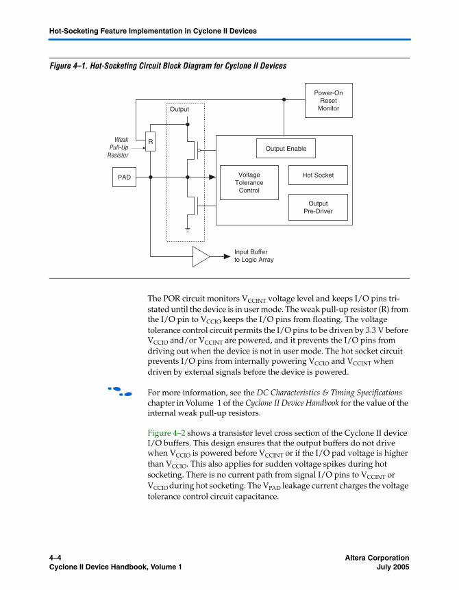
Hot-Socketing Feature Implementation in Cyclone II Devices
Figure 4–1. Hot-Socketing Circuit Block Diagram for Cyclone II Devices
The POR circuit monitors VCCINT voltage level and keeps I/O pins tri-stated until the device is in user mode. The weak pull-up resistor (R) from the I/O pin to VCCIO keeps the I/O pins from floating. The voltage tolerance control circuit permits the I/O pins to be driven by 3.3 V before VCCIO and/or VCCINT are powered, and it prevents the I/O pins from driving out when the device is not in user mode. The hot socket circuit prevents I/O pins from internally powering VCCIO and VCCINT when driven by external signals before the device is powered.
f For more information, see the DC Characteristics & Timing Specifications chapter in Volume 1 of the Cyclone II Device Handbook for the value of the internal weak pull-up resistors.
Figure 4–2 shows a transistor level cross section of the Cyclone II device I/O buffers. This design ensures that the output buffers do not drive when VCCIO is powered before VCCINT or if the I/O pad voltage is higher than VCCIO. This also applies for sudden voltage spikes during hot socketing. There is no current path from signal I/O pins to VCCINT or VCCIO during hot socketing. The VPAD leakage current charges the voltage tolerance control circuit capacitance.
Output Enable
Output
Hot Socket
OutputPre-Driver
VoltageTolerance
Control
Power-OnReset
Monitor
WeakPull-Up
Resistor
PAD
Input Bufferto Logic Array
R
4–4 Altera CorporationCyclone II Device Handbook, Volume 1 July 2005
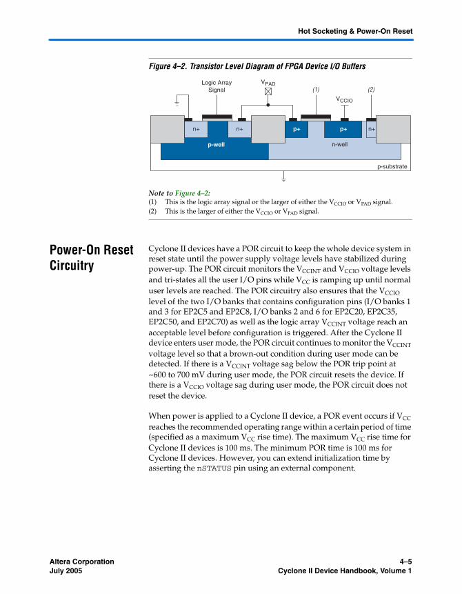
Hot Socketing & Power-On Reset
Figure 4–2. Transistor Level Diagram of FPGA Device I/O Buffers
Note to Figure 4–2:(1) This is the logic array signal or the larger of either the VCCIO or VPAD signal.(2) This is the larger of either the VCCIO or VPAD signal.
Power-On Reset Circuitry
Cyclone II devices have a POR circuit to keep the whole device system in reset state until the power supply voltage levels have stabilized during power-up. The POR circuit monitors the VCCINT and VCCIO voltage levels and tri-states all the user I/O pins while VCC is ramping up until normal user levels are reached. The POR circuitry also ensures that the VCCIO level of the two I/O banks that contains configuration pins (I/O banks 1 and 3 for EP2C5 and EP2C8, I/O banks 2 and 6 for EP2C20, EP2C35, EP2C50, and EP2C70) as well as the logic array VCCINT voltage reach an acceptable level before configuration is triggered. After the Cyclone II device enters user mode, the POR circuit continues to monitor the VCCINT voltage level so that a brown-out condition during user mode can be detected. If there is a VCCINT voltage sag below the POR trip point at ~600 to 700 mV during user mode, the POR circuit resets the device. If there is a VCCIO voltage sag during user mode, the POR circuit does not reset the device.
When power is applied to a Cyclone II device, a POR event occurs if VCC reaches the recommended operating range within a certain period of time (specified as a maximum VCC rise time). The maximum VCC rise time for Cyclone II devices is 100 ms. The minimum POR time is 100 ms for Cyclone II devices. However, you can extend initialization time by asserting the nSTATUS pin using an external component.
Logic ArraySignal (1) (2)
VCCIO
VPAD
n+ n+
n-well
n+p+p+
p-well
p-substrate
Altera Corporation 4–5July 2005 Cyclone II Device Handbook, Volume 1
Conclusion
Conclusion Cyclone II devices are hot socketable and support all power-up and power-down sequences with the one requirement that VCCIO and VCCINT be powered up and down within 100 ms of each other to keep the I/O pins from driving out. Cyclone II devices do not require any external devices for hot socketing and power sequencing.
4–6 Altera CorporationCyclone II Device Handbook, Volume 1 July 2005
Altera Corporation July 2005
CII51005-2.0
5. DC Characteristics &Timing Specifications
Operating Conditions
Cyclone™ II devices are offered in both commercial and industrial grades. Commercial devices are offered in -6 (fastest), -7, -8 speed grades.
All parameter limits are representative of worst-case supply voltage and junction temperature conditions. Unless otherwise noted, the parameter values in this chapter apply to all Cyclone II devices. AC and DC characteristics are specified using the same numbers for both commercial and industrial grades. All parameters representing voltages are measured with respect to ground.
Tables 5–1 through 5–4 provide information on absolute maximum ratings.
Table 5–1. Cyclone II Device Absolute Maximum Ratings Notes (1), (2)
Symbol Parameter Conditions Minimum Maximum Unit
VCCINT Supply voltage With respect to ground –0.5 1.8 V
VCCIO Output supply voltage –0.5 4.6 V
VIN DC input voltage (3) –0.5 4.6 V
IOUT DC output current, per pin –25 40 mA
TSTG Storage temperature No bias –65 150 °C
TJ Junction temperature BGA packages under bias 125 °C
Notes to Table 5–1:(1) Conditions beyond those listed in this table cause permanent damage to a device. These are stress ratings only.
Functional operation at these levels or any other conditions beyond those specified in this chapter is not implied. Additionally, device operation at the absolute maximum ratings for extended periods of time may have adverse affects on the device reliability.
(2) See the Operating Requirements for Altera Devices Data Sheet for more information.(3) During transitions, the inputs may over shoot to the voltage shown in Table 5–4 based upon the input duty cycle.
The DC case is equivalent to 100% duty cycle. During transition, the inputs may undershoot to –2.0 V for input currents less than 100 mA and periods shorter than 20 ns.
5–1Preliminary
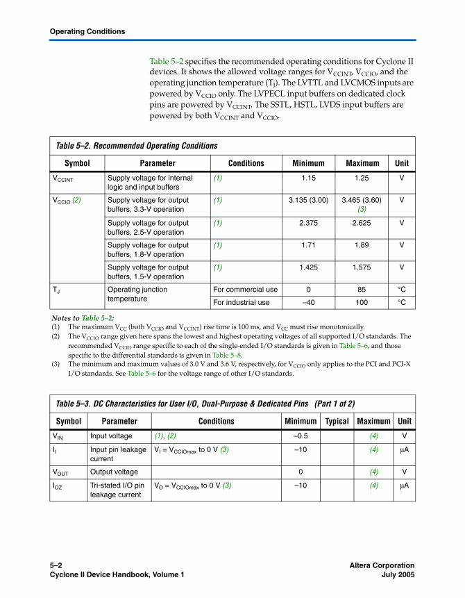
Operating Conditions
Table 5–2 specifies the recommended operating conditions for Cyclone II devices. It shows the allowed voltage ranges for VCCINT, VCCIO, and the operating junction temperature (TJ). The LVTTL and LVCMOS inputs are powered by VCCIO only. The LVPECL input buffers on dedicated clock pins are powered by VCCINT. The SSTL, HSTL, LVDS input buffers are powered by both VCCINT and VCCIO.
Table 5–2. Recommended Operating Conditions
Symbol Parameter Conditions Minimum Maximum Unit
VCCINT Supply voltage for internal logic and input buffers
(1) 1.15 1.25 V
VCCIO (2) Supply voltage for output buffers, 3.3-V operation
(1) 3.135 (3.00) 3.465 (3.60) (3)
V
Supply voltage for output buffers, 2.5-V operation
(1) 2.375 2.625 V
Supply voltage for output buffers, 1.8-V operation
(1) 1.71 1.89 V
Supply voltage for output buffers, 1.5-V operation
(1) 1.425 1.575 V
TJ Operating junction temperature
For commercial use 0 85 °C
For industrial use –40 100 °C
Notes to Table 5–2:(1) The maximum VCC (both VCCIO and VCCINT) rise time is 100 ms, and VCC must rise monotonically.(2) The VCCIO range given here spans the lowest and highest operating voltages of all supported I/O standards. The
recommended VCCIO range specific to each of the single-ended I/O standards is given in Table 5–6, and those specific to the differential standards is given in Table 5–8.
(3) The minimum and maximum values of 3.0 V and 3.6 V, respectively, for VCCIO only applies to the PCI and PCI-X I/O standards. See Table 5–6 for the voltage range of other I/O standards.
Table 5–3. DC Characteristics for User I/O, Dual-Purpose & Dedicated Pins (Part 1 of 2)
Symbol Parameter Conditions Minimum Typical Maximum Unit
VIN Input voltage (1), (2) –0.5 (4) V
II Input pin leakage current
VI = VCCIOmax to 0 V (3) –10 (4) μA
VOUT Output voltage 0 (4) V
IOZ Tri-stated I/O pin leakage current
VO = VCCIOmax to 0 V (3) –10 (4) μA
5–2 Altera CorporationCyclone II Device Handbook, Volume 1 July 2005
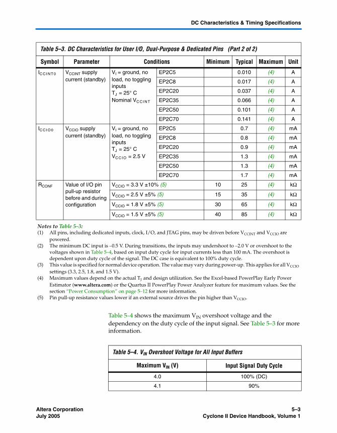
DC Characteristics & Timing Specifications
Table 5–4 shows the maximum VIN overshoot voltage and the dependency on the duty cycle of the input signal. See Table 5–3 for more information.
IC C I NT 0 VCCINT supply current (standby)
VI = ground, no load, no toggling inputsTJ = 25° C Nominal VC CI NT
EP2C5 0.010 (4) A
EP2C8 0.017 (4) A
EP2C20 0.037 (4) A
EP2C35 0.066 (4) A
EP2C50 0.101 (4) A
EP2C70 0.141 (4) A
IC CI O 0 VCCIO supply current (standby)
VI = ground, no load, no toggling inputsTJ = 25° CVC C I O = 2.5 V
EP2C5 0.7 (4) mA
EP2C8 0.8 (4) mA
EP2C20 0.9 (4) mA
EP2C35 1.3 (4) mA
EP2C50 1.3 (4) mA
EP2C70 1.7 (4) mA
RCONF Value of I/O pin pull-up resistor before and during configuration
VCCIO = 3.3 V ±10% (5) 10 25 (4) kΩ
VCCIO = 2.5 V ±5% (5) 15 35 (4) kΩ
VCCIO = 1.8 V ±5% (5) 30 65 (4) kΩ
VCCIO = 1.5 V ±5% (5) 40 85 (4) kΩ
Notes to Table 5–3:(1) All pins, including dedicated inputs, clock, I/O, and JTAG pins, may be driven before VCCINT and VCCIO are
powered.(2) The minimum DC input is –0.5 V. During transitions, the inputs may undershoot to –2.0 V or overshoot to the
voltages shown in Table 5–4, based on input duty cycle for input currents less than 100 mA. The overshoot is dependent upon duty cycle of the signal. The DC case is equivalent to 100% duty cycle.
(3) This value is specified for normal device operation. The value may vary during power-up. This applies for all VCCIO settings (3.3, 2.5, 1.8, and 1.5 V).
(4) Maximum values depend on the actual TJ and design utilization. See the Excel-based PowerPlay Early Power Estimator (www.altera.com) or the Quartus II PowerPlay Power Analyzer feature for maximum values. See the section “Power Consumption” on page 5–12 for more information.
(5) Pin pull-up resistance values lower if an external source drives the pin higher than VCCIO.
Table 5–3. DC Characteristics for User I/O, Dual-Purpose & Dedicated Pins (Part 2 of 2)
Symbol Parameter Conditions Minimum Typical Maximum Unit
Table 5–4. VIN Overshoot Voltage for All Input Buffers
Maximum VIN (V) Input Signal Duty Cycle
4.0 100% (DC)
4.1 90%
Altera Corporation 5–3July 2005 Cyclone II Device Handbook, Volume 1
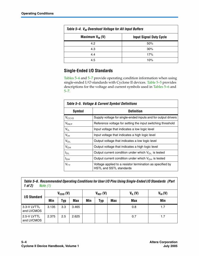
Operating Conditions
Single-Ended I/O Standards
Tables 5–6 and 5–7 provide operating condition information when using single-ended I/O standards with Cyclone II devices. Table 5–5 provides descriptions for the voltage and current symbols used in Tables 5–6 and 5–7.
4.2 50%
4.3 30%
4.4 17%
4.5 10%
Table 5–5. Voltage & Current Symbol Definitions
Symbol Definition
VCC I O Supply voltage for single-ended inputs and for output drivers
VRE F Reference voltage for setting the input switching threshold
VI L Input voltage that indicates a low logic level
VI H Input voltage that indicates a high logic level
VO L Output voltage that indicates a low logic level
VO H Output voltage that indicates a high logic level
IO L Output current condition under which VO L is tested
IO H Output current condition under which VO H is tested
VT T Voltage applied to a resistor termination as specified by HSTL and SSTL standards
Table 5–4. VIN Overshoot Voltage for All Input Buffers
Maximum VIN (V) Input Signal Duty Cycle
Table 5–6. Recommended Operating Conditions for User I/O Pins Using Single-Ended I/O Standards (Part 1 of 2) Note (1)
I/O StandardVCCIO (V) VREF (V) VIL (V) VIH (V)
Min Typ Max Min Typ Max Max Min
3.3-V LVTTL and LVCMOS
3.135 3.3 3.465 0.8 1.7
2.5-V LVTTL and LVCMOS
2.375 2.5 2.625 0.7 1.7
5–4 Altera CorporationCyclone II Device Handbook, Volume 1 July 2005
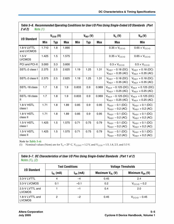
DC Characteristics & Timing Specifications
1.8-V LVTTL and LVCMOS
1.710 1.8 1.890 0.35 × VC C I O 0.65 × VC C I O
1.5-V LVCMOS
1.425 1.5 1.575 0.35 × VC C I O 0.65 × VC C I O
PCI and PCI-X 3.000 3.3 3.600 0.3 × VC C I O 0.5 × VC C I O
SSTL-2 class I 2.375 2.5 2.625 1.19 1.25 1.31 VR E F – 0.18 (DC)VRE F – 0.35 (AC)
VR E F + 0.18 (DC)VR E F + 0.35 (AC)
SSTL-2 class II 2.375 2.5 2.625 1.19 1.25 1.31 VR E F – 0.18 (DC)VRE F – 0.35 (AC)
VR E F + 0.18 (DC)VR E F + 0.35 (AC)
SSTL-18 class I
1.7 1.8 1.9 0.833 0.9 0.969 VR E F – 0.125 (DC)VRE F – 0.25 (AC)
VRE F + 0.125 (DC)VR E F + 0.25 (AC)
SSTL-18 class II
1.7 1.8 1.9 0.833 0.9 0.969 VR E F – 0.125 (DC)VRE F – 0.25 (AC)
VRE F + 0.125 (DC)VR E F + 0.25 (AC)
1.8-V HSTL class I
1.71 1.8 1.89 0.85 0.9 0.95 VR E F – 0.1 (DC)VR E F – 0.2 (AC)
VR E F + 0.1 (DC)VR E F + 0.2 (AC)
1.8-V HSTL class II
1.71 1.8 1.89 0.85 0.9 0.95 VR E F – 0.1 (DC)VR E F – 0.2 (AC)
VR E F + 0.1 (DC)VR E F + 0.2 (AC)
1.5-V HSTL class I
1.425 1.5 1.575 0.71 0.75 0.79 VR E F – 0.1 (DC)VR E F – 0.2 (AC)
VR E F + 0.1 (DC)VR E F + 0.2 (AC)
1.5-V HSTL class II
1.425 1.5 1.575 0.71 0.75 0.79 VR E F – 0.1 (DC)VR E F – 0.2 (AC)
VR E F + 0.1 (DC)VR E F + 0.2 (AC)
Note to Table 5–6:(1) Nominal values (Nom) are for TA = 25° C, VCCINT = 1.2 V, and VCCIO = 1.5, 1.8, 2.5, and 3.3 V.
Table 5–7. DC Characteristics of User I/O Pins Using Single-Ended Standards (Part 1 of 2)Notes (1), (2)
I/O Standard Test Conditions Voltage Thresholds
IOL (mA) IOH (mA) Maximum VOL (V) Minimum VOH (V)
3.3-V LVTTL 4 –4 0.45 2.4
3.3-V LVCMOS 0.1 –0.1 0.2 VC C I O – 0.2
2.5-V LVTTL and LVCMOS
1 –1 0.4 2.0
1.8-V LVTTL and LVCMOS
2 –2 0.45 VC C I O – 0.45
Table 5–6. Recommended Operating Conditions for User I/O Pins Using Single-Ended I/O Standards (Part 2 of 2) Note (1)
I/O StandardVCCIO (V) VREF (V) VIL (V) VIH (V)
Min Typ Max Min Typ Max Max Min
Altera Corporation 5–5July 2005 Cyclone II Device Handbook, Volume 1
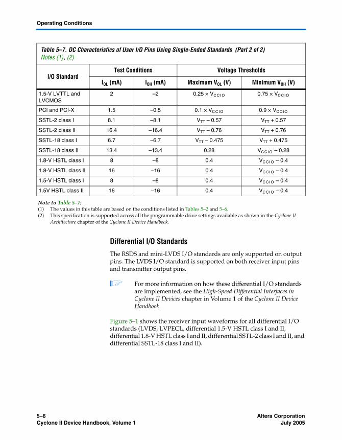
Operating Conditions
Differential I/O Standards
The RSDS and mini-LVDS I/O standards are only supported on output pins. The LVDS I/O standard is supported on both receiver input pins and transmitter output pins.
1 For more information on how these differential I/O standards are implemented, see the High-Speed Differential Interfaces in Cyclone II Devices chapter in Volume 1 of the Cyclone II Device Handbook.
Figure 5–1 shows the receiver input waveforms for all differential I/O standards (LVDS, LVPECL, differential 1.5-V HSTL class I and II, differential 1.8-V HSTL class I and II, differential SSTL-2 class I and II, and differential SSTL-18 class I and II).
1.5-V LVTTL and LVCMOS
2 –2 0.25 × VC C I O 0.75 × VC C I O
PCI and PCI-X 1.5 –0.5 0.1 × VC C I O 0.9 × VC C I O
SSTL-2 class I 8.1 –8.1 VTT – 0.57 VTT + 0.57
SSTL-2 class II 16.4 –16.4 VTT – 0.76 VTT + 0.76
SSTL-18 class I 6.7 –6.7 VTT – 0.475 VTT + 0.475
SSTL-18 class II 13.4 –13.4 0.28 VC C I O – 0.28
1.8-V HSTL class I 8 –8 0.4 VC C I O – 0.4
1.8-V HSTL class II 16 –16 0.4 VC C I O – 0.4
1.5-V HSTL class I 8 –8 0.4 VC C I O – 0.4
1.5V HSTL class II 16 –16 0.4 VC C I O – 0.4
Note to Table 5–7:(1) The values in this table are based on the conditions listed in Tables 5–2 and 5–6.(2) This specification is supported across all the programmable drive settings available as shown in the Cyclone II
Architecture chapter of the Cyclone II Device Handbook.
Table 5–7. DC Characteristics of User I/O Pins Using Single-Ended Standards (Part 2 of 2)Notes (1), (2)
I/O Standard Test Conditions Voltage Thresholds
IOL (mA) IOH (mA) Maximum VOL (V) Minimum VOH (V)
5–6 Altera CorporationCyclone II Device Handbook, Volume 1 July 2005
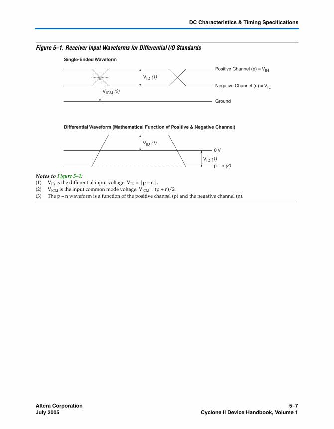
DC Characteristics & Timing Specifications
Figure 5–1. Receiver Input Waveforms for Differential I/O Standards
Notes to Figure 5–1:(1) VID is the differential input voltage. VID = |p – n|.(2) VICM is the input common mode voltage. VICM = (p + n)/2.(3) The p – n waveform is a function of the positive channel (p) and the negative channel (n).
Single-Ended Waveform
Differential Waveform (Mathematical Function of Positive & Negative Channel)
Positive Channel (p) = VIH
Negative Channel (n) = VIL
Ground
VID (1)
VID (1)
VID (1)
VICM (2)
0 V
p − n (3)
Altera Corporation 5–7July 2005 Cyclone II Device Handbook, Volume 1
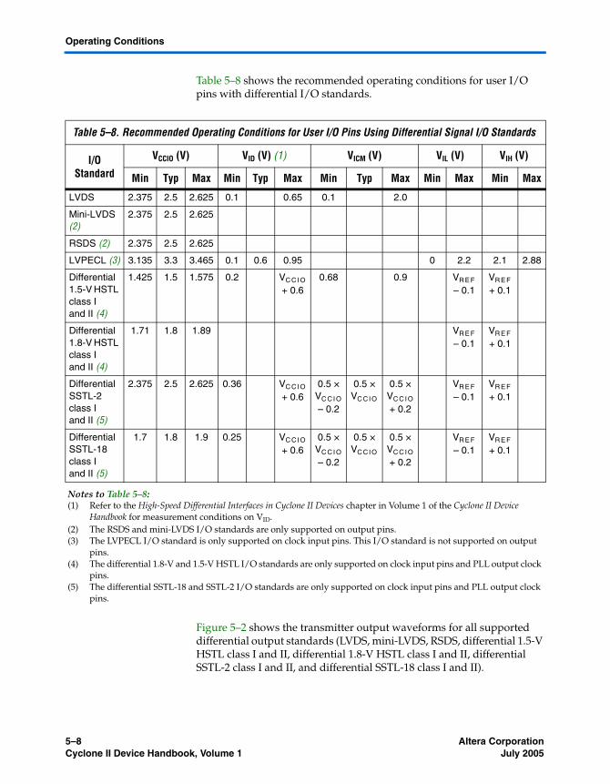
Operating Conditions
Table 5–8 shows the recommended operating conditions for user I/O pins with differential I/O standards.
Figure 5–2 shows the transmitter output waveforms for all supported differential output standards (LVDS, mini-LVDS, RSDS, differential 1.5-V HSTL class I and II, differential 1.8-V HSTL class I and II, differential SSTL-2 class I and II, and differential SSTL-18 class I and II).
Table 5–8. Recommended Operating Conditions for User I/O Pins Using Differential Signal I/O Standards
I/O Standard
VCCIO (V) VID (V) (1) VICM (V) VIL (V) VIH (V)
Min Typ Max Min Typ Max Min Typ Max Min Max Min Max
LVDS 2.375 2.5 2.625 0.1 0.65 0.1 2.0
Mini-LVDS (2)
2.375 2.5 2.625
RSDS (2) 2.375 2.5 2.625
LVPECL (3) 3.135 3.3 3.465 0.1 0.6 0.95 0 2.2 2.1 2.88
Differential 1.5-V HSTL class I and II (4)
1.425 1.5 1.575 0.2 VC C I O + 0.6
0.68 0.9 VR E F – 0.1
VR E F + 0.1
Differential 1.8-V HSTL class I and II (4)
1.71 1.8 1.89 VR E F – 0.1
VR E F + 0.1
Differential SSTL-2 class I and II (5)
2.375 2.5 2.625 0.36 VC C I O + 0.6
0.5 × VC C I O – 0.2
0.5 × VCCIO
0.5 × VC C I O + 0.2
VR E F – 0.1
VR E F + 0.1
Differential SSTL-18 class I and II (5)
1.7 1.8 1.9 0.25 VC C I O + 0.6
0.5 × VC C I O – 0.2
0.5 × VCCIO
0.5 × VC C I O + 0.2
VR E F – 0.1
VR E F + 0.1
Notes to Table 5–8:(1) Refer to the High-Speed Differential Interfaces in Cyclone II Devices chapter in Volume 1 of the Cyclone II Device
Handbook for measurement conditions on VID.(2) The RSDS and mini-LVDS I/O standards are only supported on output pins.(3) The LVPECL I/O standard is only supported on clock input pins. This I/O standard is not supported on output
pins.(4) The differential 1.8-V and 1.5-V HSTL I/O standards are only supported on clock input pins and PLL output clock
pins.(5) The differential SSTL-18 and SSTL-2 I/O standards are only supported on clock input pins and PLL output clock
pins.
5–8 Altera CorporationCyclone II Device Handbook, Volume 1 July 2005
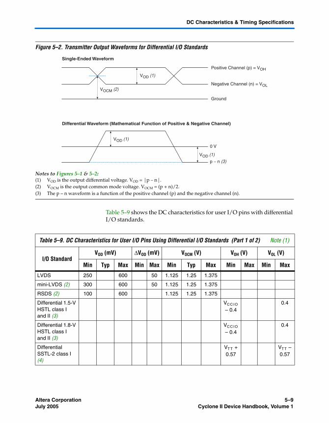
DC Characteristics & Timing Specifications
Figure 5–2. Transmitter Output Waveforms for Differential I/O Standards
Notes to Figures 5–1 & 5–2:(1) VOD is the output differential voltage. VOD = |p – n|.(2) VOCM is the output common mode voltage. VOCM = (p + n)/2.(3) The p – n waveform is a function of the positive channel (p) and the negative channel (n).
Table 5–9 shows the DC characteristics for user I/O pins with differential I/O standards.
Single-Ended Waveform
Differential Waveform (Mathematical Function of Positive & Negative Channel)
Positive Channel (p) = VOH
Negative Channel (n) = VOL
Ground
VOD (1)
VOD (1)
VOD (1)
0 V
VOCM (2)
p − n (3)
Table 5–9. DC Characteristics for User I/O Pins Using Differential I/O Standards (Part 1 of 2) Note (1)
I/O StandardVOD (mV) ΔVOD (mV) VOCM (V) VOH (V) VOL (V)
Min Typ Max Min Max Min Typ Max Min Max Min Max
LVDS 250 600 50 1.125 1.25 1.375
mini-LVDS (2) 300 600 50 1.125 1.25 1.375
RSDS (2) 100 600 1.125 1.25 1.375
Differential 1.5-V HSTL class I and II (3)
VCC I O – 0.4
0.4
Differential 1.8-V HSTL class I and II (3)
VCC I O – 0.4
0.4
Differential SSTL-2 class I (4)
VT T + 0.57
VT T – 0.57
Altera Corporation 5–9July 2005 Cyclone II Device Handbook, Volume 1
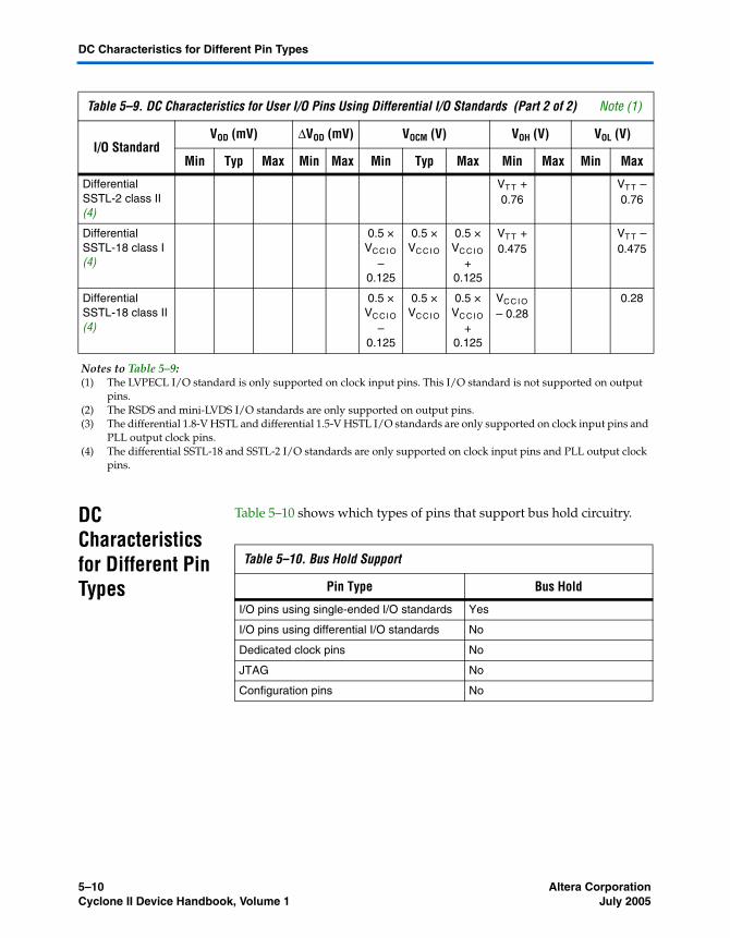
DC Characteristics for Different Pin Types
DC Characteristics for Different Pin Types
Table 5–10 shows which types of pins that support bus hold circuitry.
Differential SSTL-2 class II (4)
VT T + 0.76
VT T – 0.76
Differential SSTL-18 class I (4)
0.5 × VC C I O
– 0.125
0.5 × VC C I O
0.5 × VC C I O
+ 0.125
VT T + 0.475
VT T – 0.475
Differential SSTL-18 class II (4)
0.5 × VC C I O
– 0.125
0.5 × VC C I O
0.5 × VC C I O
+ 0.125
VCC I O – 0.28
0.28
Notes to Table 5–9:(1) The LVPECL I/O standard is only supported on clock input pins. This I/O standard is not supported on output
pins.(2) The RSDS and mini-LVDS I/O standards are only supported on output pins.(3) The differential 1.8-V HSTL and differential 1.5-V HSTL I/O standards are only supported on clock input pins and
PLL output clock pins.(4) The differential SSTL-18 and SSTL-2 I/O standards are only supported on clock input pins and PLL output clock
pins.
Table 5–9. DC Characteristics for User I/O Pins Using Differential I/O Standards (Part 2 of 2) Note (1)
I/O StandardVOD (mV) ΔVOD (mV) VOCM (V) VOH (V) VOL (V)
Min Typ Max Min Max Min Typ Max Min Max Min Max
Table 5–10. Bus Hold Support
Pin Type Bus Hold
I/O pins using single-ended I/O standards Yes
I/O pins using differential I/O standards No
Dedicated clock pins No
JTAG No
Configuration pins No
5–10 Altera CorporationCyclone II Device Handbook, Volume 1 July 2005
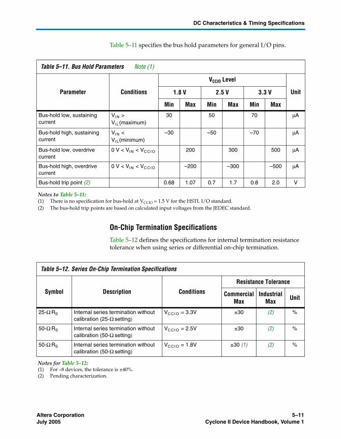
DC Characteristics & Timing Specifications
Table 5–11 specifies the bus hold parameters for general I/O pins.
On-Chip Termination Specifications
Table 5–12 defines the specifications for internal termination resistance tolerance when using series or differential on-chip termination.
Table 5–11. Bus Hold Parameters Note (1)
Parameter Conditions
VCCIO Level
Unit1.8 V 2.5 V 3.3 V
Min Max Min Max Min Max
Bus-hold low, sustaining current
VI N > VI L(maximum)
30 50 70 μA
Bus-hold high, sustaining current
VI N < VI L(minimum)
–30 –50 –70 μA
Bus-hold low, overdrive current
0 V < VI N < VC C I O 200 300 500 μA
Bus-hold high, overdrive current
0 V < VI N < VC C I O –200 –300 –500 μA
Bus-hold trip point (2) 0.68 1.07 0.7 1.7 0.8 2.0 V
Notes to Table 5–11:(1) There is no specification for bus-hold at VCCIO = 1.5 V for the HSTL I/O standard.(2) The bus-hold trip points are based on calculated input voltages from the JEDEC standard.
Table 5–12. Series On-Chip Termination Specifications
Symbol Description Conditions
Resistance Tolerance
Commercial Max
Industrial Max Unit
25-Ω RS Internal series termination without calibration (25-Ω setting)
VC CI O = 3.3V ±30 (2) %
50-Ω RS Internal series termination without calibration (50-Ω setting)
VC CI O = 2.5V ±30 (2) %
50-Ω RS Internal series termination without calibration (50-Ω setting)
VC CI O = 1.8V ±30 (1) (2) %
Notes for Table 5–12:(1) For –8 devices, the tolerance is ±40%.(2) Pending characterization.
Altera Corporation 5–11July 2005 Cyclone II Device Handbook, Volume 1
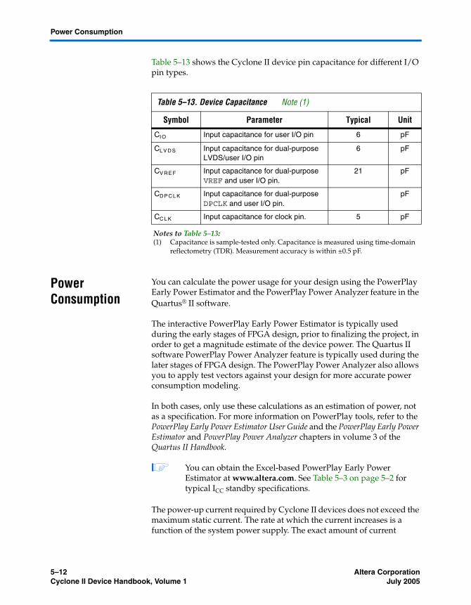
Power Consumption
Table 5–13 shows the Cyclone II device pin capacitance for different I/O pin types.
Power Consumption
You can calculate the power usage for your design using the PowerPlay Early Power Estimator and the PowerPlay Power Analyzer feature in the Quartus® II software.
The interactive PowerPlay Early Power Estimator is typically used during the early stages of FPGA design, prior to finalizing the project, in order to get a magnitude estimate of the device power. The Quartus II software PowerPlay Power Analyzer feature is typically used during the later stages of FPGA design. The PowerPlay Power Analyzer also allows you to apply test vectors against your design for more accurate power consumption modeling.
In both cases, only use these calculations as an estimation of power, not as a specification. For more information on PowerPlay tools, refer to the PowerPlay Early Power Estimator User Guide and the PowerPlay Early Power Estimator and PowerPlay Power Analyzer chapters in volume 3 of the Quartus II Handbook.
1 You can obtain the Excel-based PowerPlay Early Power Estimator at www.altera.com. See Table 5–3 on page 5–2 for typical ICC standby specifications.
The power-up current required by Cyclone II devices does not exceed the maximum static current. The rate at which the current increases is a function of the system power supply. The exact amount of current
Table 5–13. Device Capacitance Note (1)
Symbol Parameter Typical Unit
CI O Input capacitance for user I/O pin 6 pF
CL V D S Input capacitance for dual-purpose LVDS/user I/O pin
6 pF
CV RE F Input capacitance for dual-purpose VREF and user I/O pin.
21 pF
CD P C L K Input capacitance for dual-purpose DPCLK and user I/O pin.
pF
CC L K Input capacitance for clock pin. 5 pF
Notes to Table 5–13:(1) Capacitance is sample-tested only. Capacitance is measured using time-domain
reflectometry (TDR). Measurement accuracy is within ±0.5 pF.
5–12 Altera CorporationCyclone II Device Handbook, Volume 1 July 2005
DC Characteristics & Timing Specifications
consumed varies according to the process, temperature, and power ramp rate. The duration of the ICCINT power-up requirement depends on the VCCINT voltage supply rise time.
You should select power supplies and regulators that can supply the amount of current required when designing with Cyclone II devices.
Altera recommends using the Cyclone II PowerPlay Early Power Estimator to estimate the user-mode ICCINT consumption and then select power supplies or regulators based on the values obtained.
Timing Specifications
The DirectDrive™ technology and MultiTrack™ interconnect ensure predictable performance, accurate simulation, and accurate timing analysis across all Cyclone II device densities and speed grades. This section describes and specifies the performance, internal, external, high-speed I/O, JTAG, and PLL timing specifications.
This section shows the timing models for Cyclone II devices. Commercial devices meet this timing over the commercial temperature range. Industrial devices meet this timing over the industrial temperature range. All specifications are representative of worst-case supply voltage and junction temperature conditions.
1 The timing numbers listed in the tables of this section are extracted from the Quartus® II software version 5.0 SP1.
Preliminary & Final Timing Specifications
Timing models can have either preliminary or final status. The Quartus II software issues an informational message during the design compilation if the timing models are preliminary. Table 5–14 shows the status of the Cyclone II device timing models.
Preliminary status means the timing model is subject to change. Initially, timing numbers are created using simulation results, process data, and other known parameters. These tests are used to make the preliminary numbers as close to the actual timing parameters as possible.
Altera Corporation 5–13July 2005 Cyclone II Device Handbook, Volume 1
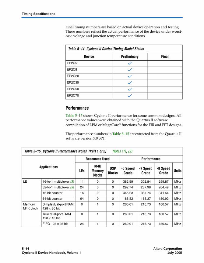
Timing Specifications
Final timing numbers are based on actual device operation and testing. These numbers reflect the actual performance of the device under worst-case voltage and junction temperature conditions.
Performance
Table 5–15 shows Cyclone II performance for some common designs. All performance values were obtained with the Quartus II software compilation of LPM or MegaCore® functions for the FIR and FFT designs.
The performance numbers in Table 5–15 are extracted from the Quartus II software version 5.0 SP1.
Table 5–14. Cyclone II Device Timing Model Status
Device Preliminary Final
EP2C5 v
EP2C8 v
EP2C20 v
EP2C35 v
EP2C50 v
EP2C70 v
Table 5–15. Cyclone II Performance Notes (Part 1 of 2) Notes (1), (2)
Applications
Resources Used Performance
LEsM4K
Memory Blocks
DSP Blocks
-6 Speed Grade
-7 Speed Grade
-8 Speed Grade Units
LE 16-to-1 multiplexer (3) 11 0 0 382.99 302.84 259.87 MHz
32-to-1 multiplexer (3) 24 0 0 292.74 237.98 204.49 MHz
16-bit counter 16 0 0 445.23 387.74 341.64 MHz
64-bit counter 64 0 0 188.82 168.37 150.92 MHz
Memory M4K block
Simple dual-port RAM 128 × 36 bit
0 1 0 260.01 216.73 180.57 MHz
True dual-port RAM 128 × 18 bit
0 1 0 260.01 216.73 180.57 MHz
FIFO 128 x 36 bit 24 1 0 260.01 216.73 180.57 MHz
5–14 Altera CorporationCyclone II Device Handbook, Volume 1 July 2005
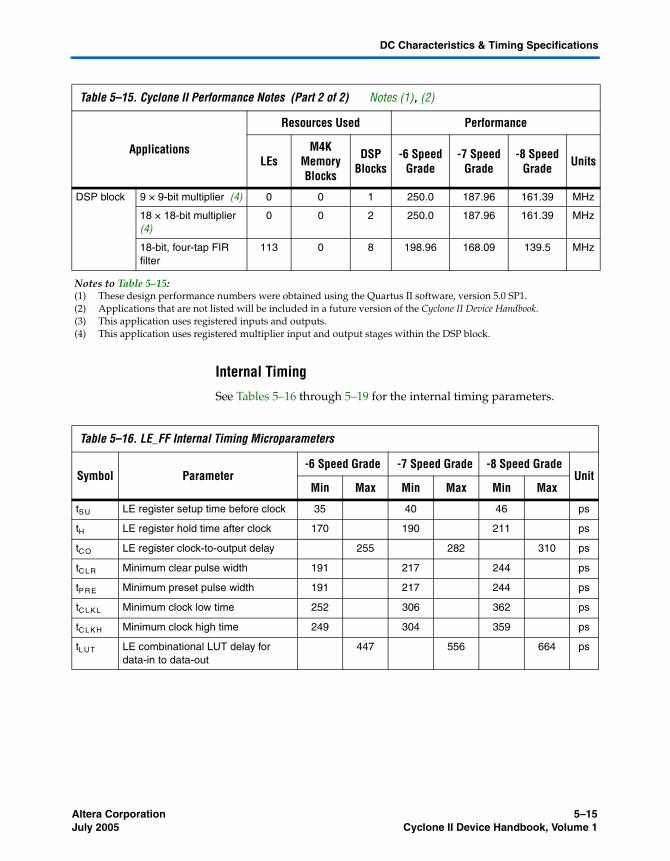
DC Characteristics & Timing Specifications
Internal Timing
See Tables 5–16 through 5–19 for the internal timing parameters.
DSP block 9 × 9-bit multiplier (4) 0 0 1 250.0 187.96 161.39 MHz
18 × 18-bit multiplier (4)
0 0 2 250.0 187.96 161.39 MHz
18-bit, four-tap FIR filter
113 0 8 198.96 168.09 139.5 MHz
Notes to Table 5–15:(1) These design performance numbers were obtained using the Quartus II software, version 5.0 SP1.(2) Applications that are not listed will be included in a future version of the Cyclone II Device Handbook.(3) This application uses registered inputs and outputs.(4) This application uses registered multiplier input and output stages within the DSP block.
Table 5–15. Cyclone II Performance Notes (Part 2 of 2) Notes (1), (2)
Applications
Resources Used Performance
LEsM4K
Memory Blocks
DSP Blocks
-6 Speed Grade
-7 Speed Grade
-8 Speed Grade Units
Table 5–16. LE_FF Internal Timing Microparameters
Symbol Parameter-6 Speed Grade -7 Speed Grade -8 Speed Grade
UnitMin Max Min Max Min Max
tS U LE register setup time before clock 35 40 46 ps
tH LE register hold time after clock 170 190 211 ps
tC O LE register clock-to-output delay 255 282 310 ps
tC L R Minimum clear pulse width 191 217 244 ps
tP R E Minimum preset pulse width 191 217 244 ps
tC L K L Minimum clock low time 252 306 362 ps
tC L K H Minimum clock high time 249 304 359 ps
tL U T LE combinational LUT delay for data-in to data-out
447 556 664 ps
Altera Corporation 5–15July 2005 Cyclone II Device Handbook, Volume 1
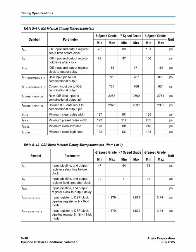
Timing Specifications
Table 5–17. IOE Internal Timing Microparameters
Symbol Parameter-6 Speed Grade -7 Speed Grade -8 Speed Grade
UnitMin Max Min Max Min Max
tS U IOE input and output register setup time before clock
76 89 101 ps
tH IOE input and output register hold time after clock
88 97 106 ps
tC O IOE input and output register clock-to-output delay
155 171 187 ps
tP I N 2 C O M B O U T _ R Row input pin to IOE combinational output
725 767 855 ps
tP I N 2 C O M B O U T _ C Column input pin to IOE combinational output
724 766 854 ps
tC O M B I N2 P I N _ R Row IOE data input to combinational output pin
2253 2502 2751 ps
tC O M B I N2 P I N _ C Column IOE data input to combinational output pin
2372 2637 2902 ps
tC L R Minimum clear pulse width 137 151 165 ps
tP R E Minimum preset pulse width 192 212 233 ps
tC L K L Minimum clock low time 178 191 216 ps
tC L K H Minimum clock high time 122 131 143 ps
Table 5–18. DSP Block Internal Timing Microparameters (Part 1 of 2)
Symbol Parameter-6 Speed Grade -7 Speed Grade -8 Speed Grade
UnitMin Max Min Max Min Max
tS U Input, pipeline, and output register setup time before clock
47 54 62 ps
tH Input, pipeline, and output register hold time after clock
10 11 13 ps
tC O Input, pipeline, and output register clock-to-output delay
ps
tI N R E G 2 P I P E 9 Input register to DSP block pipeline register in 9 × 9-bit mode
1,379 1,872 2,441 ps
tI N R E G 2 P I P E 1 8 Input register to DSP block pipeline register in 18 × 18-bit mode
1,379 1,872 2,441 ps
5–16 Altera CorporationCyclone II Device Handbook, Volume 1 July 2005

DC Characteristics & Timing Specifications
tP I P E 2 O U T R E G DSP block pipeline register to output register delay
104 142 185 ps
tP D 9 Combinational input to output delay for 9 × 9
2,963 4,022 5,242 ps
tP D 1 8 Combinational input to output delay for 18 × 18
3,492 4,739 6,177 ps
tC L R Minimum clear pulse width 2,686 3,129 3,572 ps
tC L K L Minimum clock low time 2,000 2,660 3,098 ps
tC L K H Minimum clock high time 2,000 2,660 3,098 ps
Table 5–19. M4K Block Internal Timing Microparameters (Part 1 of 2)
Symbol Parameter-6 Speed Grade -7 Speed Grade -8 Speed Grade
UnitMin Max Min Max Min Max
tM 4 K R C Synchronous read cycle time 3,764 4,248 4,736 ps
tM 4 K W E R E S U Write or read enable setup time before clock
35 40 46 ps
tM 4 K W E R E H Write or read enable hold time after clock
134 150 167 ps
tM 4 K B E S U Byte enable setup time before clock
35 40 46 ps
tM 4 K B E H Byte enable hold time after clock 134 150 167 ps
tM 4 K DATA A S U A port data setup time before clock
35 40 46 ps
tM 4 K DATA A H A port data hold time after clock 134 150 167 ps
tM 4 K A D D R A S U A port address setup time before clock
35 40 46 ps
tM 4 K A D D R A H A port address hold time after clock
134 150 167 ps
tM 4 K DATA B S U B port data setup time before clock
35 40 46 ps
tM 4 K DATA B H B port data hold time after clock 134 150 167 ps
tM 4 K R A D D RB S U B port address setup time before clock
35 40 46 ps
tM 4 K R A D D RB H B port address hold time after clock
134 150 167 ps
Table 5–18. DSP Block Internal Timing Microparameters (Part 2 of 2)
Symbol Parameter-6 Speed Grade -7 Speed Grade -8 Speed Grade
UnitMin Max Min Max Min Max
Altera Corporation 5–17July 2005 Cyclone II Device Handbook, Volume 1
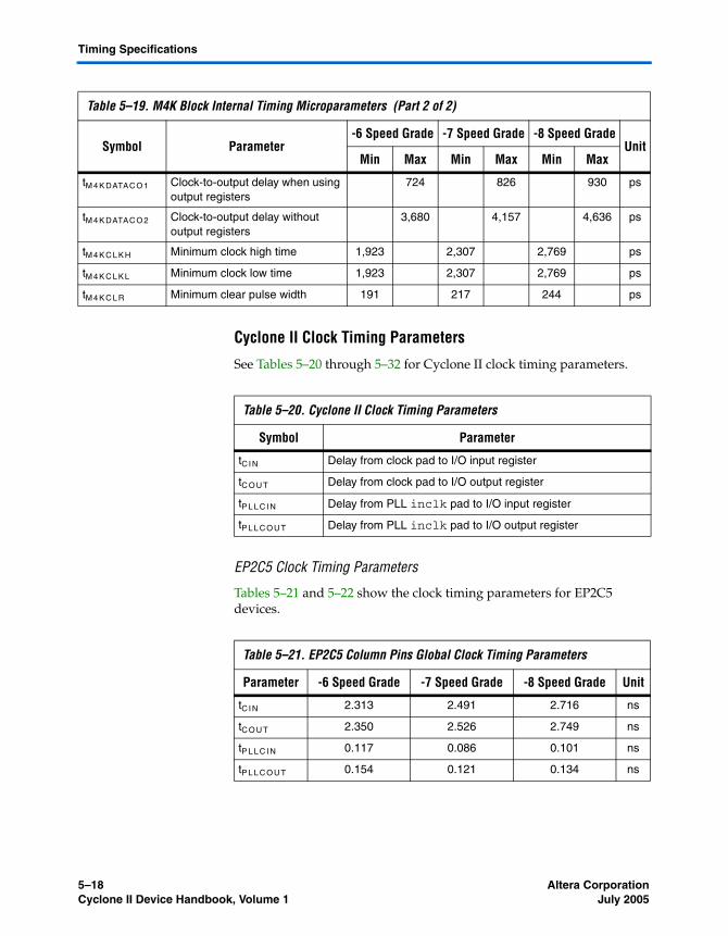
Timing Specifications
Cyclone II Clock Timing Parameters
See Tables 5–20 through 5–32 for Cyclone II clock timing parameters.
EP2C5 Clock Timing Parameters
Tables 5–21 and 5–22 show the clock timing parameters for EP2C5 devices.
tM 4 K DATAC O 1 Clock-to-output delay when using output registers
724 826 930 ps
tM 4 K DATAC O 2 Clock-to-output delay without output registers
3,680 4,157 4,636 ps
tM 4 K C L K H Minimum clock high time 1,923 2,307 2,769 ps
tM 4 K C L K L Minimum clock low time 1,923 2,307 2,769 ps
tM 4 K C L R Minimum clear pulse width 191 217 244 ps
Table 5–19. M4K Block Internal Timing Microparameters (Part 2 of 2)
Symbol Parameter-6 Speed Grade -7 Speed Grade -8 Speed Grade
UnitMin Max Min Max Min Max
Table 5–20. Cyclone II Clock Timing Parameters
Symbol Parameter
tC I N Delay from clock pad to I/O input register
tC O UT Delay from clock pad to I/O output register
tP L L C I N Delay from PLL inclk pad to I/O input register
tP L L C O U T Delay from PLL inclk pad to I/O output register
Table 5–21. EP2C5 Column Pins Global Clock Timing Parameters
Parameter -6 Speed Grade -7 Speed Grade -8 Speed Grade Unit
tC I N 2.313 2.491 2.716 ns
tC O UT 2.350 2.526 2.749 ns
tP L L C I N 0.117 0.086 0.101 ns
tP L L C O U T 0.154 0.121 0.134 ns
5–18 Altera CorporationCyclone II Device Handbook, Volume 1 July 2005
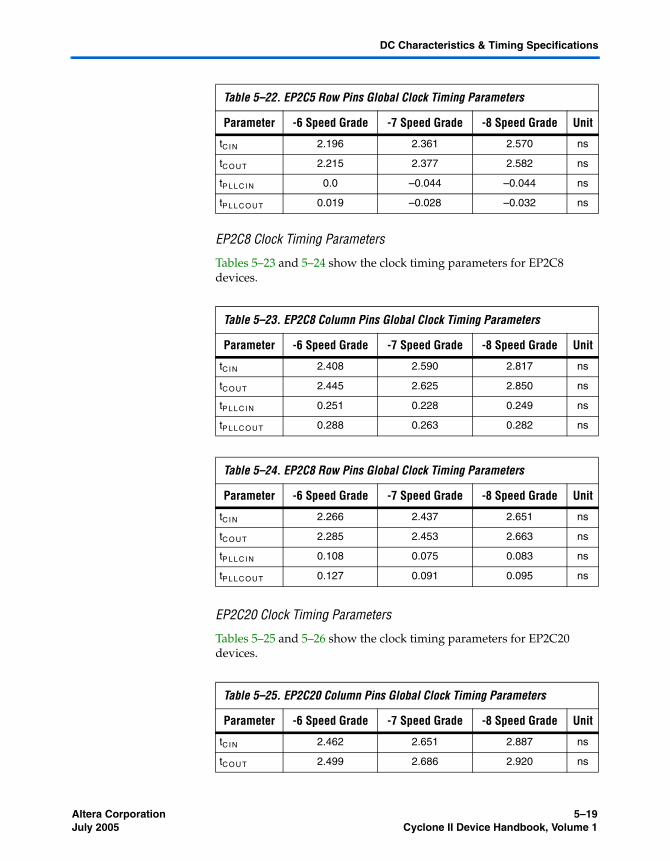
DC Characteristics & Timing Specifications
EP2C8 Clock Timing Parameters
Tables 5–23 and 5–24 show the clock timing parameters for EP2C8 devices.
EP2C20 Clock Timing Parameters
Tables 5–25 and 5–26 show the clock timing parameters for EP2C20 devices.
Table 5–22. EP2C5 Row Pins Global Clock Timing Parameters
Parameter -6 Speed Grade -7 Speed Grade -8 Speed Grade Unit
tC I N 2.196 2.361 2.570 ns
tC O UT 2.215 2.377 2.582 ns
tP L L C I N 0.0 –0.044 –0.044 ns
tP L L C O U T 0.019 –0.028 –0.032 ns
Table 5–23. EP2C8 Column Pins Global Clock Timing Parameters
Parameter -6 Speed Grade -7 Speed Grade -8 Speed Grade Unit
tC I N 2.408 2.590 2.817 ns
tC O UT 2.445 2.625 2.850 ns
tP L L C I N 0.251 0.228 0.249 ns
tP L L C O U T 0.288 0.263 0.282 ns
Table 5–24. EP2C8 Row Pins Global Clock Timing Parameters
Parameter -6 Speed Grade -7 Speed Grade -8 Speed Grade Unit
tC I N 2.266 2.437 2.651 ns
tC O UT 2.285 2.453 2.663 ns
tP L L C I N 0.108 0.075 0.083 ns
tP L L C O U T 0.127 0.091 0.095 ns
Table 5–25. EP2C20 Column Pins Global Clock Timing Parameters
Parameter -6 Speed Grade -7 Speed Grade -8 Speed Grade Unit
tC I N 2.462 2.651 2.887 ns
tC O UT 2.499 2.686 2.920 ns
Altera Corporation 5–19July 2005 Cyclone II Device Handbook, Volume 1

Timing Specifications
EP2C35 Clock Timing Parameters
Tables 5–27 and 5–28 show the clock timing parameters for EP2C35 devices.
tP L L C I N 0.15 0.116 0.128 ns
tP L L C O U T 0.187 0.151 0.161 ns
Table 5–26. EP2C20 Row Pins Global Clock Timing Parameters
Parameter -6 Speed Grade -7 Speed Grade -8 Speed Grade Unit
tC I N 2.351 2.527 2.750 ns
tC O UT 2.370 2.543 2.762 ns
tP L L C I N 0.039 –0.008 –0.009 ns
tP L L C O U T 0.058 0.008 0.003 ns
Table 5–27. EP2C35 Column Pins Global Clock Timing Parameters
Parameter -6 Speed Grade -7 Speed Grade -8 Speed Grade Unit
tC I N 2.602 2.800 3.048 ns
tC O UT 2.639 2.835 3.081 ns
tP L L C I N 0.294 0.27 0.296 ns
tP L L C O U T 0.331 0.305 0.329 ns
Table 5–28. EP2C35 Row Pins Global Clock Timing Parameters
Parameter -6 Speed Grade -7 Speed Grade -8 Speed Grade Unit
tC I N 2.469 2.655 2.888 ns
tC O UT 2.488 2.671 2.900 ns
tP L L C I N 0.161 0.125 0.137 ns
tP L L C O U T 0.18 0.141 0.149 ns
Table 5–25. EP2C20 Column Pins Global Clock Timing Parameters
Parameter -6 Speed Grade -7 Speed Grade -8 Speed Grade Unit
5–20 Altera CorporationCyclone II Device Handbook, Volume 1 July 2005
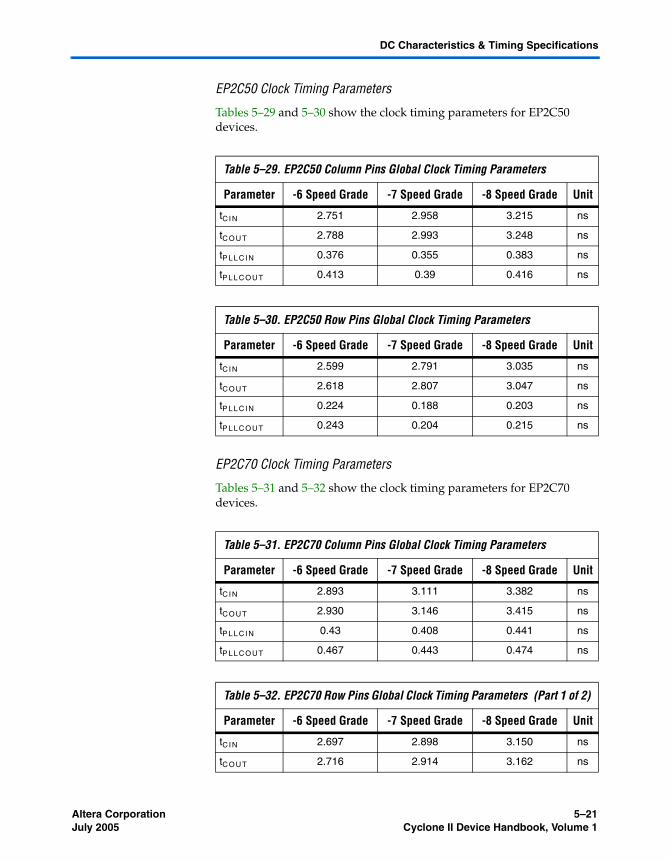
DC Characteristics & Timing Specifications
EP2C50 Clock Timing Parameters
Tables 5–29 and 5–30 show the clock timing parameters for EP2C50 devices.
EP2C70 Clock Timing Parameters
Tables 5–31 and 5–32 show the clock timing parameters for EP2C70 devices.
Table 5–29. EP2C50 Column Pins Global Clock Timing Parameters
Parameter -6 Speed Grade -7 Speed Grade -8 Speed Grade Unit
tC I N 2.751 2.958 3.215 ns
tC O UT 2.788 2.993 3.248 ns
tP L L C I N 0.376 0.355 0.383 ns
tP L L C O U T 0.413 0.39 0.416 ns
Table 5–30. EP2C50 Row Pins Global Clock Timing Parameters
Parameter -6 Speed Grade -7 Speed Grade -8 Speed Grade Unit
tC I N 2.599 2.791 3.035 ns
tC O UT 2.618 2.807 3.047 ns
tP L L C I N 0.224 0.188 0.203 ns
tP L L C O U T 0.243 0.204 0.215 ns
Table 5–31. EP2C70 Column Pins Global Clock Timing Parameters
Parameter -6 Speed Grade -7 Speed Grade -8 Speed Grade Unit
tC I N 2.893 3.111 3.382 ns
tC O UT 2.930 3.146 3.415 ns
tP L L C I N 0.43 0.408 0.441 ns
tP L L C O U T 0.467 0.443 0.474 ns
Table 5–32. EP2C70 Row Pins Global Clock Timing Parameters (Part 1 of 2)
Parameter -6 Speed Grade -7 Speed Grade -8 Speed Grade Unit
tC I N 2.697 2.898 3.150 ns
tC O UT 2.716 2.914 3.162 ns
Altera Corporation 5–21July 2005 Cyclone II Device Handbook, Volume 1

Timing Specifications
IOE Programmable Delay
See Tables 5–33 and 5–34 for IOE programmable delay.
tP L L C I N 0.232 0.195 0.207 ns
tP L L C O U T 0.251 0.211 0.219 ns
Table 5–32. EP2C70 Row Pins Global Clock Timing Parameters (Part 2 of 2)
Parameter -6 Speed Grade -7 Speed Grade -8 Speed Grade Unit
Table 5–33. Cyclone II IOE Programmable Delay on Column Pins Note (1)
Parameter Paths Affected Available Settings
-6 Speed Grade -7 Speed Grade -8 Speed Grade
UnitMin Offset
Max Offset
Min Offset
Max Offset
Min Offset
Max Offset
Input delay from pin to internal cells
Pad to I/O dataout to logic array
7 0 3,826 0 4,087 0 4,349 ps
Input delay from pin to input register
Pad to I/O input register
56 0 8,110 0 8,650 0 9,190 ps
Delay from output register to output pin
I/O output register to pad
2 0 563 0 617 0 670 ps
Note to Table 5–33:(1) The incremental values for the settings are generally linear. For the exact delay associated with each setting, use
the latest version of the Quartus II software.
Table 5–34. Cyclone II IOE Programmable Delay on Row Pins Note (1) (Part 1 of 2)
Parameter Paths Affected Available Settings
-6 Speed Grade -7 Speed Grade -8 Speed Grade
UnitMin Offset
Max Offset
Min Offset
Max Offset
Min Offset
Max Offset
Input delay from pin to internal cells
Pad to I/O dataout to logic array
7 0 3,775 0 4,033 0 4,290 ps
Input delay from pin to input register
Pad to I/O input register
56 0 7,990 0 8,522 0 9,052 ps
5–22 Altera CorporationCyclone II Device Handbook, Volume 1 July 2005
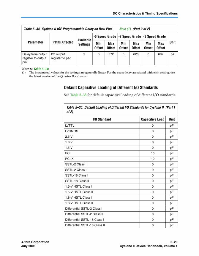
DC Characteristics & Timing Specifications
Default Capacitive Loading of Different I/O Standards
See Table 5–35 for default capacitive loading of different I/O standards.
Delay from output register to output pin
I/O output register to pad
2 0 572 0 626 0 682 ps
Note to Table 5–34:(1) The incremental values for the settings are generally linear. For the exact delay associated with each setting, use
the latest version of the Quartus II software.
Table 5–34. Cyclone II IOE Programmable Delay on Row Pins Note (1) (Part 2 of 2)
Parameter Paths Affected Available Settings
-6 Speed Grade -7 Speed Grade -8 Speed Grade
UnitMin Offset
Max Offset
Min Offset
Max Offset
Min Offset
Max Offset
Table 5–35. Default Loading of Different I/O Standards for Cyclone II (Part 1 of 2)
I/O Standard Capacitive Load Unit
LVTTL 0 pF
LVCMOS 0 pF
2.5 V 0 pF
1.8 V 0 pF
1.5 V 0 pF
PCI 10 pF
PCI-X 10 pF
SSTL-2 Class I 0 pF
SSTL-2 Class II 0 pF
SSTL-18 Class I 0 pF
SSTL-18 Class II 0 pF
1.5-V HSTL Class I 0 pF
1.5-V HSTL Class II 0 pF
1.8-V HSTL Class I 0 pF
1.8-V HSTL Class II 0 pF
Differential SSTL-2 Class I 0 pF
Differential SSTL-2 Class II 0 pF
Differential SSTL-18 Class I 0 pF
Differential SSTL-18 Class II 0 pF
Altera Corporation 5–23July 2005 Cyclone II Device Handbook, Volume 1

Timing Specifications
I/O Delays
See Tables 5–36 through 5–40 for I/O delays.
1.5-V differential HSTL Class I 0 pF
1.5-V differential HSTL Class II 0 pF
1.8-V differential HSTL Class I 0 pF
1.8-V differential HSTL Class II 0 pF
LVDS 0 pF
Table 5–36. I/O Delay Parameters
Symbol Parameter
tD I P Delay from I/O datain to output pad
tO P Delay from I/O output register to output pad
tP CO U T Delay from input pad to I/O dataout to core
tP I Delay from input pad to I/O input register
Table 5–35. Default Loading of Different I/O Standards for Cyclone II (Part 2 of 2)
I/O Standard Capacitive Load Unit
Table 5–37. Cyclone II I/O Input Delay for Column Pins (Part 1 of 2)
I/O Standard Parameter -6 Speed Grade
-7 Speed Grade
-8 Speed Grade Unit
LVTTL tP I 1,079 1,157 1,282 ps
tP C O UT 724 766 854 ps
2.5 V tP I 1,050 1,166 1,283 ps
tP C O UT 695 775 855 ps
1.8 V tP I 1,221 1,352 1,484 ps
tP C O UT 866 961 1,056 ps
1.5 V tP I 1,285 1,420 1,556 ps
tP C O UT 930 1,029 1,128 ps
LVCMOS tP I 1,079 1,157 1,282 ps
tP C O UT 724 766 854 ps
SSTL-2 Class I tP I 858 949 1,040 ps
tP C O UT 503 558 612 ps
5–24 Altera CorporationCyclone II Device Handbook, Volume 1 July 2005
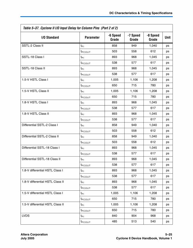
DC Characteristics & Timing Specifications
SSTL-2 Class II tP I 858 949 1,040 ps
tP C O UT 503 558 612 ps
SSTL-18 Class I tP I 893 968 1,045 ps
tP C O UT 538 577 617 ps
SSTL-18 Class II tP I 893 968 1,045 ps
tP C O UT 538 577 617 ps
1.5-V HSTL Class I tP I 1,005 1,106 1,208 ps
tP C O UT 650 715 780 ps
1.5-V HSTL Class II tP I 1,005 1,106 1,208 ps
tP C O UT 650 715 780 ps
1.8-V HSTL Class I tP I 893 968 1,045 ps
tP C O UT 538 577 617 ps
1.8-V HSTL Class II tP I 893 968 1,045 ps
tP C O UT 538 577 617 ps
Differential SSTL-2 Class I tP I 858 949 1,040 ps
tP C O UT 503 558 612 ps
Differential SSTL-2 Class II tP I 858 949 1,040 ps
tP C O UT 503 558 612 ps
Differential SSTL-18 Class I tP I 893 968 1,045 ps
tP C O UT 538 577 617 ps
Differential SSTL-18 Class II tP I 893 968 1,045 ps
tP C O UT 538 577 617 ps
1.8-V differential HSTL Class I tP I 893 968 1,045 ps
tP C O UT 538 577 617 ps
1.8-V differential HSTL Class II tP I 893 968 1,045 ps
tP C O UT 538 577 617 ps
1.5-V differential HSTL Class I tP I 1,005 1,106 1,208 ps
tP C O UT 650 715 780 ps
1.5-V differential HSTL Class II tP I 1,005 1,106 1,208 ps
tP C O UT 650 715 780 ps
LVDS tP I 840 904 968 ps
tP C O UT 485 513 540 ps
Table 5–37. Cyclone II I/O Input Delay for Column Pins (Part 2 of 2)
I/O Standard Parameter -6 Speed Grade
-7 Speed Grade
-8 Speed Grade Unit
Altera Corporation 5–25July 2005 Cyclone II Device Handbook, Volume 1
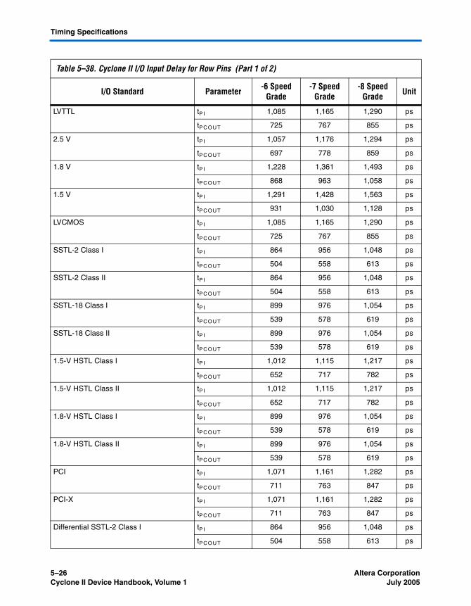
Timing Specifications
Table 5–38. Cyclone II I/O Input Delay for Row Pins (Part 1 of 2)
I/O Standard Parameter -6 Speed Grade
-7 Speed Grade
-8 Speed Grade Unit
LVTTL tP I 1,085 1,165 1,290 ps
tP C O UT 725 767 855 ps
2.5 V tP I 1,057 1,176 1,294 ps
tP C O UT 697 778 859 ps
1.8 V tP I 1,228 1,361 1,493 ps
tP C O UT 868 963 1,058 ps
1.5 V tP I 1,291 1,428 1,563 ps
tP C O UT 931 1,030 1,128 ps
LVCMOS tP I 1,085 1,165 1,290 ps
tP C O UT 725 767 855 ps
SSTL-2 Class I tP I 864 956 1,048 ps
tP C O UT 504 558 613 ps
SSTL-2 Class II tP I 864 956 1,048 ps
tP C O UT 504 558 613 ps
SSTL-18 Class I tP I 899 976 1,054 ps
tP C O UT 539 578 619 ps
SSTL-18 Class II tP I 899 976 1,054 ps
tP C O UT 539 578 619 ps
1.5-V HSTL Class I tP I 1,012 1,115 1,217 ps
tP C O UT 652 717 782 ps
1.5-V HSTL Class II tP I 1,012 1,115 1,217 ps
tP C O UT 652 717 782 ps
1.8-V HSTL Class I tP I 899 976 1,054 ps
tP C O UT 539 578 619 ps
1.8-V HSTL Class II tP I 899 976 1,054 ps
tP C O UT 539 578 619 ps
PCI tP I 1,071 1,161 1,282 ps
tP C O UT 711 763 847 ps
PCI-X tP I 1,071 1,161 1,282 ps
tP C O UT 711 763 847 ps
Differential SSTL-2 Class I tP I 864 956 1,048 ps
tP C O UT 504 558 613 ps
5–26 Altera CorporationCyclone II Device Handbook, Volume 1 July 2005
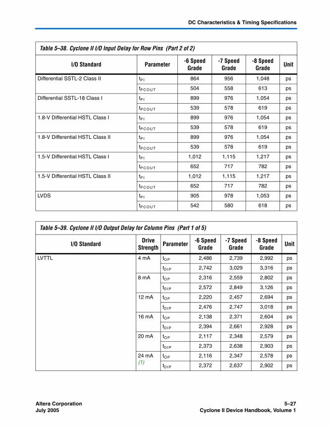
DC Characteristics & Timing Specifications
Differential SSTL-2 Class II tP I 864 956 1,048 ps
tP C O UT 504 558 613 ps
Differential SSTL-18 Class I tP I 899 976 1,054 ps
tP C O UT 539 578 619 ps
1.8-V Differential HSTL Class I tP I 899 976 1,054 ps
tP C O UT 539 578 619 ps
1.8-V Differential HSTL Class II tP I 899 976 1,054 ps
tP C O UT 539 578 619 ps
1.5-V Differential HSTL Class I tP I 1,012 1,115 1,217 ps
tP C O UT 652 717 782 ps
1.5-V Differential HSTL Class II tP I 1,012 1,115 1,217 ps
tP C O UT 652 717 782 ps
LVDS tP I 905 978 1,053 ps
tP C O UT 542 580 618 ps
Table 5–39. Cyclone II I/O Output Delay for Column Pins (Part 1 of 5)
I/O Standard Drive Strength Parameter -6 Speed
Grade -7 Speed
Grade -8 Speed
Grade Unit
LVTTL 4 mA tO P 2,486 2,739 2,992 ps
tD I P 2,742 3,029 3,316 ps
8 mA tO P 2,316 2,559 2,802 ps
tD I P 2,572 2,849 3,126 ps
12 mA tO P 2,220 2,457 2,694 ps
tD I P 2,476 2,747 3,018 ps
16 mA tO P 2,138 2,371 2,604 ps
tD I P 2,394 2,661 2,928 ps
20 mA tO P 2,117 2,348 2,579 ps
tD I P 2,373 2,638 2,903 ps
24 mA (1)
tO P 2,116 2,347 2,578 ps
tD I P 2,372 2,637 2,902 ps
Table 5–38. Cyclone II I/O Input Delay for Row Pins (Part 2 of 2)
I/O Standard Parameter -6 Speed Grade
-7 Speed Grade
-8 Speed Grade Unit
Altera Corporation 5–27July 2005 Cyclone II Device Handbook, Volume 1
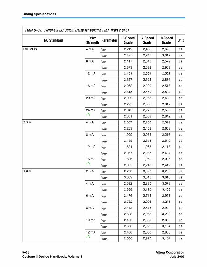
Timing Specifications
LVCMOS 4 mA tO P 2,219 2,456 2,693 ps
tD I P 2,475 2,746 3,017 ps
8 mA tO P 2,117 2,348 2,579 ps
tD I P 2,373 2,638 2,903 ps
12 mA tO P 2,101 2,331 2,562 ps
tD I P 2,357 2,624 2,886 ps
16 mA tO P 2,062 2,290 2,518 ps
tD I P 2,318 2,580 2,842 ps
20 mA tO P 2,039 2,266 2,493 ps
tD I P 2,295 2,556 2,817 ps
24 mA (1)
tO P 2,045 2,272 2,500 ps
tD I P 2,301 2,562 2,842 ps
2.5 V 4 mA tO P 2,007 2,168 2,329 ps
tD I P 2,263 2,458 2,653 ps
8 mA tO P 1,909 2,062 2,216 ps
tD I P 2,165 2,352 2,540 ps
12 mA tO P 1,821 1,967 2,113 ps
tD I P 2,077 2,257 2,437 ps
16 mA (1)
tO P 1,806 1,950 2,095 ps
tD I P 2,065 2,240 2,419 ps
1.8 V 2 mA tO P 2,753 3,023 3,292 ps
tD I P 3,009 3,313 3,616 ps
4 mA tO P 2,582 2,830 3,079 ps
tD I P 2,838 3,120 3,403 ps
6 mA tO P 2,476 2,714 2,951 ps
tD I P 2,732 3,004 3,275 ps
8 mA tO P 2,442 2,675 2,909 ps
tD I P 2,698 2,965 3,233 ps
10 mA tO P 2,400 2,630 2,860 ps
tD I P 2,656 2,920 3,184 ps
12 mA (1)
tO P 2,400 2,630 2,860 ps
tD I P 2,656 2,920 3,184 ps
Table 5–39. Cyclone II I/O Output Delay for Column Pins (Part 2 of 5)
I/O Standard Drive Strength Parameter -6 Speed
Grade -7 Speed
Grade -8 Speed
Grade Unit
5–28 Altera CorporationCyclone II Device Handbook, Volume 1 July 2005
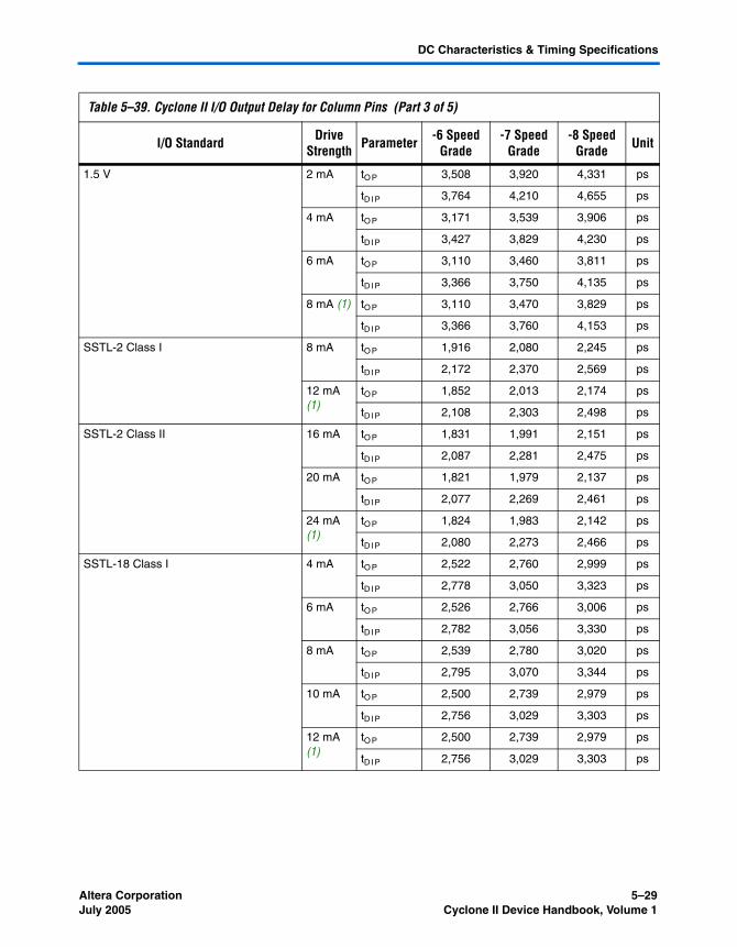
DC Characteristics & Timing Specifications
1.5 V 2 mA tO P 3,508 3,920 4,331 ps
tD I P 3,764 4,210 4,655 ps
4 mA tO P 3,171 3,539 3,906 ps
tD I P 3,427 3,829 4,230 ps
6 mA tO P 3,110 3,460 3,811 ps
tD I P 3,366 3,750 4,135 ps
8 mA (1) tO P 3,110 3,470 3,829 ps
tD I P 3,366 3,760 4,153 ps
SSTL-2 Class I 8 mA tO P 1,916 2,080 2,245 ps
tD I P 2,172 2,370 2,569 ps
12 mA (1)
tO P 1,852 2,013 2,174 ps
tD I P 2,108 2,303 2,498 ps
SSTL-2 Class II 16 mA tO P 1,831 1,991 2,151 ps
tD I P 2,087 2,281 2,475 ps
20 mA tO P 1,821 1,979 2,137 ps
tD I P 2,077 2,269 2,461 ps
24 mA (1)
tO P 1,824 1,983 2,142 ps
tD I P 2,080 2,273 2,466 ps
SSTL-18 Class I 4 mA tO P 2,522 2,760 2,999 ps
tD I P 2,778 3,050 3,323 ps
6 mA tO P 2,526 2,766 3,006 ps
tD I P 2,782 3,056 3,330 ps
8 mA tO P 2,539 2,780 3,020 ps
tD I P 2,795 3,070 3,344 ps
10 mA tO P 2,500 2,739 2,979 ps
tD I P 2,756 3,029 3,303 ps
12 mA (1)
tO P 2,500 2,739 2,979 ps
tD I P 2,756 3,029 3,303 ps
Table 5–39. Cyclone II I/O Output Delay for Column Pins (Part 3 of 5)
I/O Standard Drive Strength Parameter -6 Speed
Grade -7 Speed
Grade -8 Speed
Grade Unit
Altera Corporation 5–29July 2005 Cyclone II Device Handbook, Volume 1
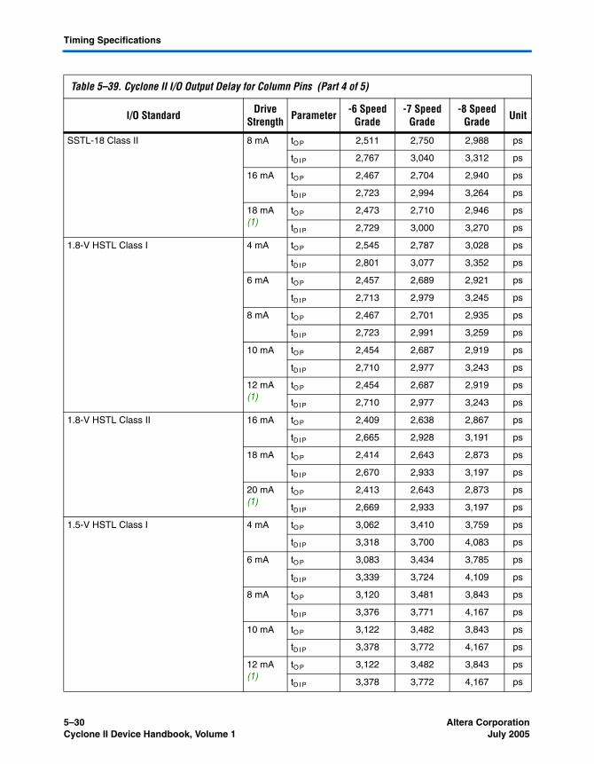
Timing Specifications
SSTL-18 Class II 8 mA tO P 2,511 2,750 2,988 ps
tD I P 2,767 3,040 3,312 ps
16 mA tO P 2,467 2,704 2,940 ps
tD I P 2,723 2,994 3,264 ps
18 mA (1)
tO P 2,473 2,710 2,946 ps
tD I P 2,729 3,000 3,270 ps
1.8-V HSTL Class I 4 mA tO P 2,545 2,787 3,028 ps
tD I P 2,801 3,077 3,352 ps
6 mA tO P 2,457 2,689 2,921 ps
tD I P 2,713 2,979 3,245 ps
8 mA tO P 2,467 2,701 2,935 ps
tD I P 2,723 2,991 3,259 ps
10 mA tO P 2,454 2,687 2,919 ps
tD I P 2,710 2,977 3,243 ps
12 mA (1)
tO P 2,454 2,687 2,919 ps
tD I P 2,710 2,977 3,243 ps
1.8-V HSTL Class II 16 mA tO P 2,409 2,638 2,867 ps
tD I P 2,665 2,928 3,191 ps
18 mA tO P 2,414 2,643 2,873 ps
tD I P 2,670 2,933 3,197 ps
20 mA (1)
tO P 2,413 2,643 2,873 ps
tD I P 2,669 2,933 3,197 ps
1.5-V HSTL Class I 4 mA tO P 3,062 3,410 3,759 ps
tD I P 3,318 3,700 4,083 ps
6 mA tO P 3,083 3,434 3,785 ps
tD I P 3,339 3,724 4,109 ps
8 mA tO P 3,120 3,481 3,843 ps
tD I P 3,376 3,771 4,167 ps
10 mA tO P 3,122 3,482 3,843 ps
tD I P 3,378 3,772 4,167 ps
12 mA (1)
tO P 3,122 3,482 3,843 ps
tD I P 3,378 3,772 4,167 ps
Table 5–39. Cyclone II I/O Output Delay for Column Pins (Part 4 of 5)
I/O Standard Drive Strength Parameter -6 Speed
Grade -7 Speed
Grade -8 Speed
Grade Unit
5–30 Altera CorporationCyclone II Device Handbook, Volume 1 July 2005
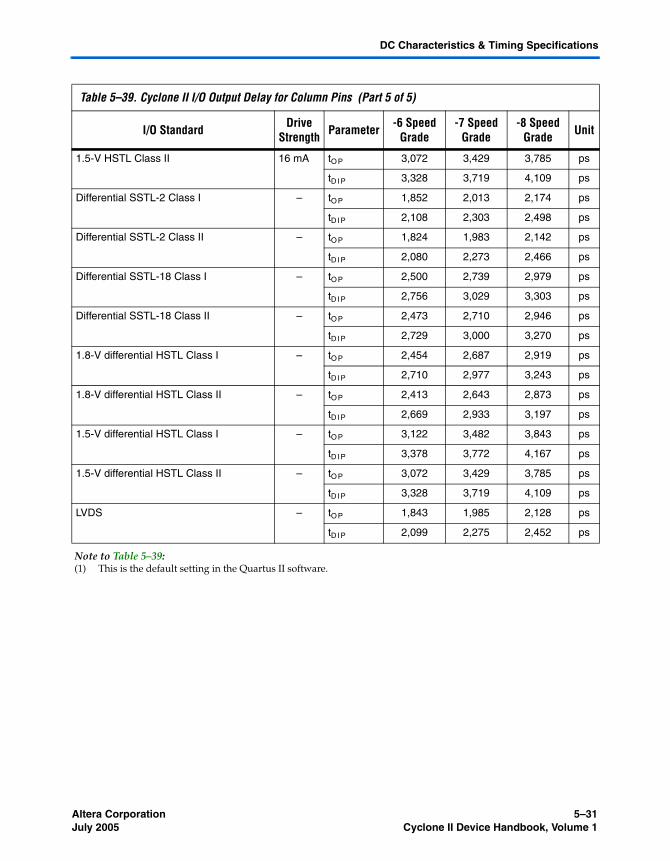
DC Characteristics & Timing Specifications
1.5-V HSTL Class II 16 mA tO P 3,072 3,429 3,785 ps
tD I P 3,328 3,719 4,109 ps
Differential SSTL-2 Class I – tO P 1,852 2,013 2,174 ps
tD I P 2,108 2,303 2,498 ps
Differential SSTL-2 Class II – tO P 1,824 1,983 2,142 ps
tD I P 2,080 2,273 2,466 ps
Differential SSTL-18 Class I – tO P 2,500 2,739 2,979 ps
tD I P 2,756 3,029 3,303 ps
Differential SSTL-18 Class II – tO P 2,473 2,710 2,946 ps
tD I P 2,729 3,000 3,270 ps
1.8-V differential HSTL Class I – tO P 2,454 2,687 2,919 ps
tD I P 2,710 2,977 3,243 ps
1.8-V differential HSTL Class II – tO P 2,413 2,643 2,873 ps
tD I P 2,669 2,933 3,197 ps
1.5-V differential HSTL Class I – tO P 3,122 3,482 3,843 ps
tD I P 3,378 3,772 4,167 ps
1.5-V differential HSTL Class II – tO P 3,072 3,429 3,785 ps
tD I P 3,328 3,719 4,109 ps
LVDS – tO P 1,843 1,985 2,128 ps
tD I P 2,099 2,275 2,452 ps
Note to Table 5–39:(1) This is the default setting in the Quartus II software.
Table 5–39. Cyclone II I/O Output Delay for Column Pins (Part 5 of 5)
I/O Standard Drive Strength Parameter -6 Speed
Grade -7 Speed
Grade -8 Speed
Grade Unit
Altera Corporation 5–31July 2005 Cyclone II Device Handbook, Volume 1
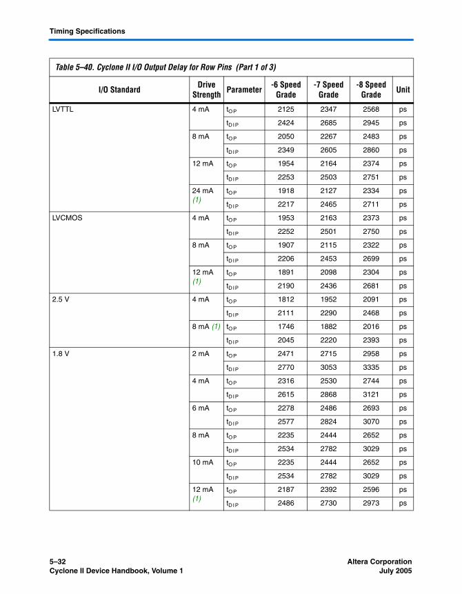
Timing Specifications
Table 5–40. Cyclone II I/O Output Delay for Row Pins (Part 1 of 3)
I/O Standard Drive Strength Parameter -6 Speed
Grade -7 Speed
Grade -8 Speed
Grade Unit
LVTTL 4 mA tO P 2125 2347 2568 ps
tD I P 2424 2685 2945 ps
8 mA tO P 2050 2267 2483 ps
tD I P 2349 2605 2860 ps
12 mA tO P 1954 2164 2374 ps
tD I P 2253 2503 2751 ps
24 mA (1)
tO P 1918 2127 2334 ps
tD I P 2217 2465 2711 ps
LVCMOS 4 mA tO P 1953 2163 2373 ps
tD I P 2252 2501 2750 ps
8 mA tO P 1907 2115 2322 ps
tD I P 2206 2453 2699 ps
12 mA (1)
tO P 1891 2098 2304 ps
tD I P 2190 2436 2681 ps
2.5 V 4 mA tO P 1812 1952 2091 ps
tD I P 2111 2290 2468 ps
8 mA (1) tO P 1746 1882 2016 ps
tD I P 2045 2220 2393 ps
1.8 V 2 mA tO P 2471 2715 2958 ps
tD I P 2770 3053 3335 ps
4 mA tO P 2316 2530 2744 ps
tD I P 2615 2868 3121 ps
6 mA tO P 2278 2486 2693 ps
tD I P 2577 2824 3070 ps
8 mA tO P 2235 2444 2652 ps
tD I P 2534 2782 3029 ps
10 mA tO P 2235 2444 2652 ps
tD I P 2534 2782 3029 ps
12 mA (1)
tO P 2187 2392 2596 ps
tD I P 2486 2730 2973 ps
5–32 Altera CorporationCyclone II Device Handbook, Volume 1 July 2005
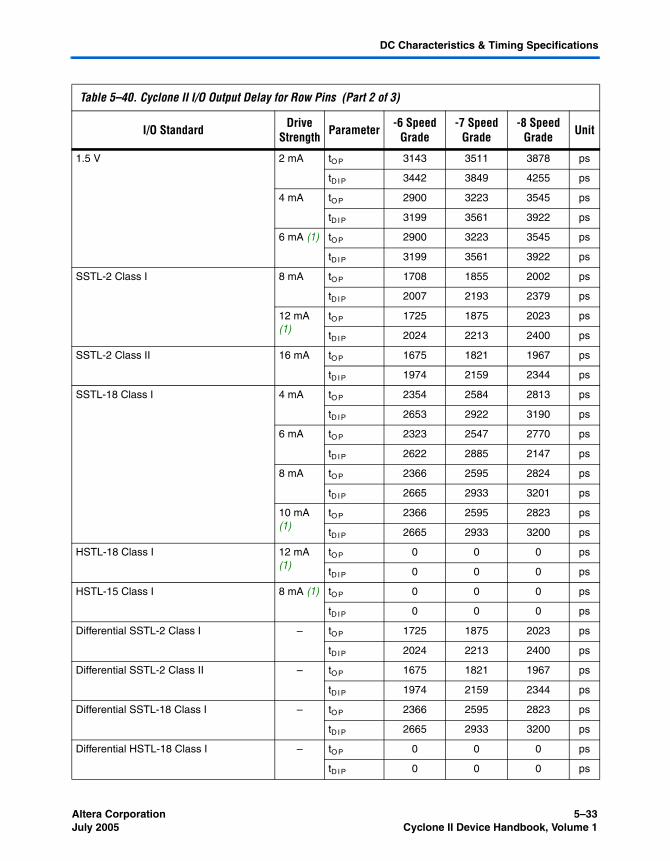
DC Characteristics & Timing Specifications
1.5 V 2 mA tO P 3143 3511 3878 ps
tD I P 3442 3849 4255 ps
4 mA tO P 2900 3223 3545 ps
tD I P 3199 3561 3922 ps
6 mA (1) tO P 2900 3223 3545 ps
tD I P 3199 3561 3922 ps
SSTL-2 Class I 8 mA tO P 1708 1855 2002 ps
tD I P 2007 2193 2379 ps
12 mA (1)
tO P 1725 1875 2023 ps
tD I P 2024 2213 2400 ps
SSTL-2 Class II 16 mA tO P 1675 1821 1967 ps
tD I P 1974 2159 2344 ps
SSTL-18 Class I 4 mA tO P 2354 2584 2813 ps
tD I P 2653 2922 3190 ps
6 mA tO P 2323 2547 2770 ps
tD I P 2622 2885 2147 ps
8 mA tO P 2366 2595 2824 ps
tD I P 2665 2933 3201 ps
10 mA (1)
tO P 2366 2595 2823 ps
tD I P 2665 2933 3200 ps
HSTL-18 Class I 12 mA (1)
tO P 0 0 0 ps
tD I P 0 0 0 ps
HSTL-15 Class I 8 mA (1) tO P 0 0 0 ps
tD I P 0 0 0 ps
Differential SSTL-2 Class I – tO P 1725 1875 2023 ps
tD I P 2024 2213 2400 ps
Differential SSTL-2 Class II – tO P 1675 1821 1967 ps
tD I P 1974 2159 2344 ps
Differential SSTL-18 Class I – tO P 2366 2595 2823 ps
tD I P 2665 2933 3200 ps
Differential HSTL-18 Class I – tO P 0 0 0 ps
tD I P 0 0 0 ps
Table 5–40. Cyclone II I/O Output Delay for Row Pins (Part 2 of 3)
I/O Standard Drive Strength Parameter -6 Speed
Grade -7 Speed
Grade -8 Speed
Grade Unit
Altera Corporation 5–33July 2005 Cyclone II Device Handbook, Volume 1
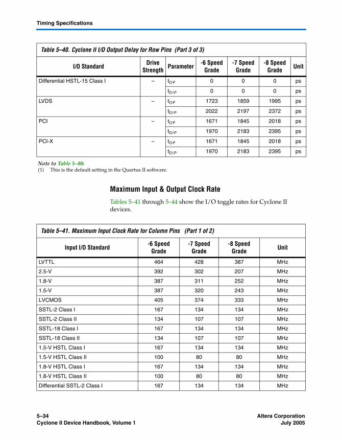
Timing Specifications
Maximum Input & Output Clock Rate
Tables 5–41 through 5–44 show the I/O toggle rates for Cyclone II devices.
Differential HSTL-15 Class I – tO P 0 0 0 ps
tD I P 0 0 0 ps
LVDS – tO P 1723 1859 1995 ps
tD I P 2022 2197 2372 ps
PCI – tO P 1671 1845 2018 ps
tD I P 1970 2183 2395 ps
PCI-X – tO P 1671 1845 2018 ps
tD I P 1970 2183 2395 ps
Note to Table 5–40:(1) This is the default setting in the Quartus II software.
Table 5–40. Cyclone II I/O Output Delay for Row Pins (Part 3 of 3)
I/O Standard Drive Strength Parameter -6 Speed
Grade -7 Speed
Grade -8 Speed
Grade Unit
Table 5–41. Maximum Input Clock Rate for Column Pins (Part 1 of 2)
Input I/O Standard -6 Speed Grade
-7 Speed Grade
-8 Speed Grade Unit
LVTTL 464 428 387 MHz
2.5-V 392 302 207 MHz
1.8-V 387 311 252 MHz
1.5-V 387 320 243 MHz
LVCMOS 405 374 333 MHz
SSTL-2 Class I 167 134 134 MHz
SSTL-2 Class II 134 107 107 MHz
SSTL-18 Class I 167 134 134 MHz
SSTL-18 Class II 134 107 107 MHz
1.5-V HSTL Class I 167 134 134 MHz
1.5-V HSTL Class II 100 80 80 MHz
1.8-V HSTL Class I 167 134 134 MHz
1.8-V HSTL Class II 100 80 80 MHz
Differential SSTL-2 Class I 167 134 134 MHz
5–34 Altera CorporationCyclone II Device Handbook, Volume 1 July 2005
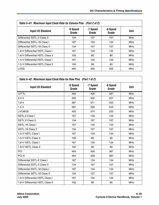
DC Characteristics & Timing Specifications
Differential SSTL-2 Class II 134 107 107 MHz
Differential SSTL-18 Class I 167 134 134 MHz
Differential SSTL-18 Class II 134 107 107 MHz
1.8-V Differential HSTL Class I 167 134 134 MHz
1.8-V Differential HSTL Class II 100 80 80 MHz
1.5-V Differential HSTL Class I 167 134 134 MHz
1.5-V Differential HSTL Class II 100 80 80 MHz
LVDS 402 402 402 MHz
Table 5–42. Maximum Input Clock Rate for Row Pins (Part 1 of 2)
Input I/O Standard -6 Speed Grade
-7 Speed Grade
-8 Speed Grade Unit
LVTTL 464 428 387 MHz
2.5-V 392 302 207 MHz
1.8-V 387 311 252 MHz
1.5-V 387 320 243 MHz
LVCMOS 405 374 333 MHz
SSTL-2 Class I 167 134 134 MHz
SSTL-2 Class II 134 107 107 MHz
SSTL-18 Class I 167 134 134 MHz
SSTL-18 Class II 134 107 107 MHz
1.5-V HSTL Class I 167 134 134 MHz
1.5-V HSTL Class II 100 80 80 MHz
1.8-V HSTL Class I 167 134 134 MHz
1.8-V HSTL Class II 100 80 80 MHz
PCI 464 428 387 MHz
PCI-X 464 428 387 MHz
Differential SSTL-2 Class I 167 134 134 MHz
Differential SSTL-2 Class II 134 107 107 MHz
Differential SSTL-18 Class I 167 134 134 MHz
Differential SSTL-18 Class II 134 107 107 MHz
1.8-V Differential HSTL Class I 167 134 134 MHz
1.8-V Differential HSTL Class II 100 80 80 MHz
Table 5–41. Maximum Input Clock Rate for Column Pins (Part 2 of 2)
Input I/O Standard -6 Speed Grade
-7 Speed Grade
-8 Speed Grade Unit
Altera Corporation 5–35July 2005 Cyclone II Device Handbook, Volume 1
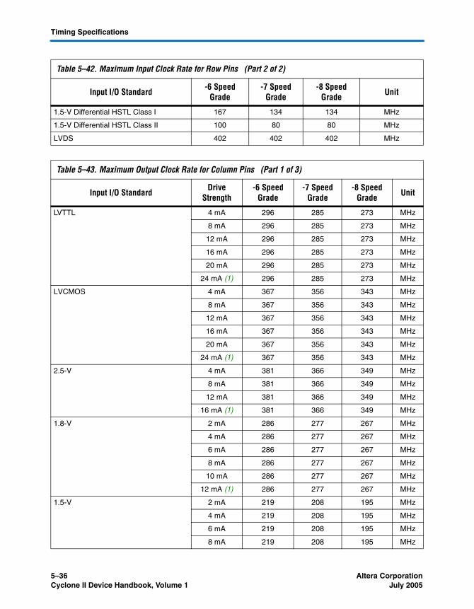
Timing Specifications
1.5-V Differential HSTL Class I 167 134 134 MHz
1.5-V Differential HSTL Class II 100 80 80 MHz
LVDS 402 402 402 MHz
Table 5–43. Maximum Output Clock Rate for Column Pins (Part 1 of 3)
Input I/O Standard Drive Strength
-6 Speed Grade
-7 Speed Grade
-8 Speed Grade Unit
LVTTL 4 mA 296 285 273 MHz
8 mA 296 285 273 MHz
12 mA 296 285 273 MHz
16 mA 296 285 273 MHz
20 mA 296 285 273 MHz
24 mA (1) 296 285 273 MHz
LVCMOS 4 mA 367 356 343 MHz
8 mA 367 356 343 MHz
12 mA 367 356 343 MHz
16 mA 367 356 343 MHz
20 mA 367 356 343 MHz
24 mA (1) 367 356 343 MHz
2.5-V 4 mA 381 366 349 MHz
8 mA 381 366 349 MHz
12 mA 381 366 349 MHz
16 mA (1) 381 366 349 MHz
1.8-V 2 mA 286 277 267 MHz
4 mA 286 277 267 MHz
6 mA 286 277 267 MHz
8 mA 286 277 267 MHz
10 mA 286 277 267 MHz
12 mA (1) 286 277 267 MHz
1.5-V 2 mA 219 208 195 MHz
4 mA 219 208 195 MHz
6 mA 219 208 195 MHz
8 mA 219 208 195 MHz
Table 5–42. Maximum Input Clock Rate for Row Pins (Part 2 of 2)
Input I/O Standard -6 Speed Grade
-7 Speed Grade
-8 Speed Grade Unit
5–36 Altera CorporationCyclone II Device Handbook, Volume 1 July 2005
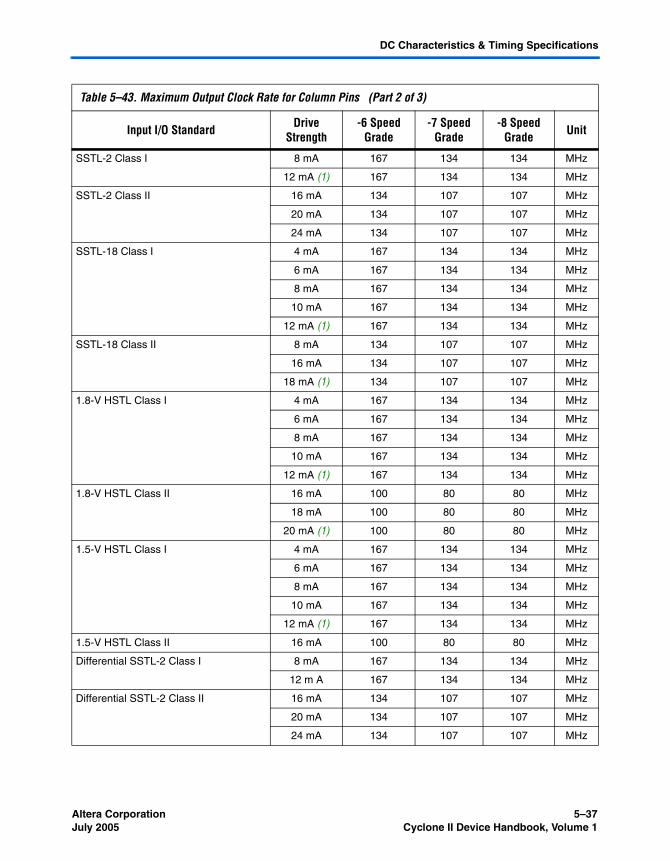
DC Characteristics & Timing Specifications
SSTL-2 Class I 8 mA 167 134 134 MHz
12 mA (1) 167 134 134 MHz
SSTL-2 Class II 16 mA 134 107 107 MHz
20 mA 134 107 107 MHz
24 mA 134 107 107 MHz
SSTL-18 Class I 4 mA 167 134 134 MHz
6 mA 167 134 134 MHz
8 mA 167 134 134 MHz
10 mA 167 134 134 MHz
12 mA (1) 167 134 134 MHz
SSTL-18 Class II 8 mA 134 107 107 MHz
16 mA 134 107 107 MHz
18 mA (1) 134 107 107 MHz
1.8-V HSTL Class I 4 mA 167 134 134 MHz
6 mA 167 134 134 MHz
8 mA 167 134 134 MHz
10 mA 167 134 134 MHz
12 mA (1) 167 134 134 MHz
1.8-V HSTL Class II 16 mA 100 80 80 MHz
18 mA 100 80 80 MHz
20 mA (1) 100 80 80 MHz
1.5-V HSTL Class I 4 mA 167 134 134 MHz
6 mA 167 134 134 MHz
8 mA 167 134 134 MHz
10 mA 167 134 134 MHz
12 mA (1) 167 134 134 MHz
1.5-V HSTL Class II 16 mA 100 80 80 MHz
Differential SSTL-2 Class I 8 mA 167 134 134 MHz
12 m A 167 134 134 MHz
Differential SSTL-2 Class II 16 mA 134 107 107 MHz
20 mA 134 107 107 MHz
24 mA 134 107 107 MHz
Table 5–43. Maximum Output Clock Rate for Column Pins (Part 2 of 3)
Input I/O Standard Drive Strength
-6 Speed Grade
-7 Speed Grade
-8 Speed Grade Unit
Altera Corporation 5–37July 2005 Cyclone II Device Handbook, Volume 1
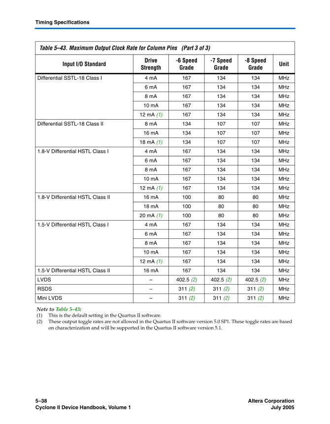
Timing Specifications
Differential SSTL-18 Class I 4 mA 167 134 134 MHz
6 mA 167 134 134 MHz
8 mA 167 134 134 MHz
10 mA 167 134 134 MHz
12 mA (1) 167 134 134 MHz
Differential SSTL-18 Class II 8 mA 134 107 107 MHz
16 mA 134 107 107 MHz
18 mA (1) 134 107 107 MHz
1.8-V Differential HSTL Class I 4 mA 167 134 134 MHz
6 mA 167 134 134 MHz
8 mA 167 134 134 MHz
10 mA 167 134 134 MHz
12 mA (1) 167 134 134 MHz
1.8-V Differential HSTL Class II 16 mA 100 80 80 MHz
18 mA 100 80 80 MHz
20 mA (1) 100 80 80 MHz
1.5-V Differential HSTL Class I 4 mA 167 134 134 MHz
6 mA 167 134 134 MHz
8 mA 167 134 134 MHz
10 mA 167 134 134 MHz
12 mA (1) 167 134 134 MHz
1.5-V Differential HSTL Class II 16 mA 167 134 134 MHz
LVDS – 402.5 (2) 402.5 (2) 402.5 (2) MHz
RSDS – 311 (2) 311 (2) 311 (2) MHz
Mini LVDS – 311 (2) 311 (2) 311 (2) MHz
Note to Table 5–43:(1) This is the default setting in the Quartus II software.(2) These output toggle rates are not allowed in the Quartus II software version 5.0 SP1. These toggle rates are based
on characterization and will be supported in the Quartus II software version 5.1.
Table 5–43. Maximum Output Clock Rate for Column Pins (Part 3 of 3)
Input I/O Standard Drive Strength
-6 Speed Grade
-7 Speed Grade
-8 Speed Grade Unit
5–38 Altera CorporationCyclone II Device Handbook, Volume 1 July 2005
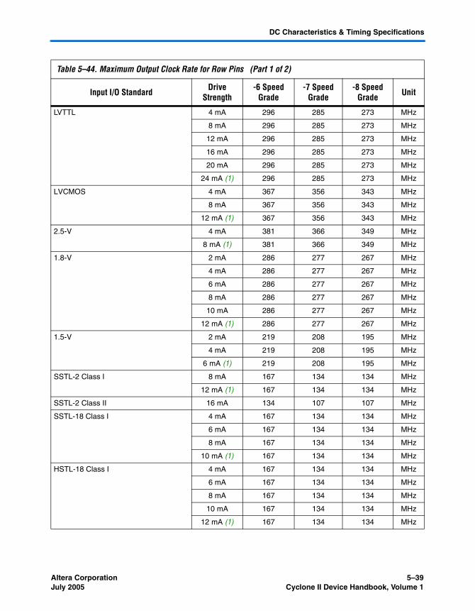
DC Characteristics & Timing Specifications
Table 5–44. Maximum Output Clock Rate for Row Pins (Part 1 of 2)
Input I/O Standard Drive Strength
-6 Speed Grade
-7 Speed Grade
-8 Speed Grade Unit
LVTTL 4 mA 296 285 273 MHz
8 mA 296 285 273 MHz
12 mA 296 285 273 MHz
16 mA 296 285 273 MHz
20 mA 296 285 273 MHz
24 mA (1) 296 285 273 MHz
LVCMOS 4 mA 367 356 343 MHz
8 mA 367 356 343 MHz
12 mA (1) 367 356 343 MHz
2.5-V 4 mA 381 366 349 MHz
8 mA (1) 381 366 349 MHz
1.8-V 2 mA 286 277 267 MHz
4 mA 286 277 267 MHz
6 mA 286 277 267 MHz
8 mA 286 277 267 MHz
10 mA 286 277 267 MHz
12 mA (1) 286 277 267 MHz
1.5-V 2 mA 219 208 195 MHz
4 mA 219 208 195 MHz
6 mA (1) 219 208 195 MHz
SSTL-2 Class I 8 mA 167 134 134 MHz
12 mA (1) 167 134 134 MHz
SSTL-2 Class II 16 mA 134 107 107 MHz
SSTL-18 Class I 4 mA 167 134 134 MHz
6 mA 167 134 134 MHz
8 mA 167 134 134 MHz
10 mA (1) 167 134 134 MHz
HSTL-18 Class I 4 mA 167 134 134 MHz
6 mA 167 134 134 MHz
8 mA 167 134 134 MHz
10 mA 167 134 134 MHz
12 mA (1) 167 134 134 MHz
Altera Corporation 5–39July 2005 Cyclone II Device Handbook, Volume 1
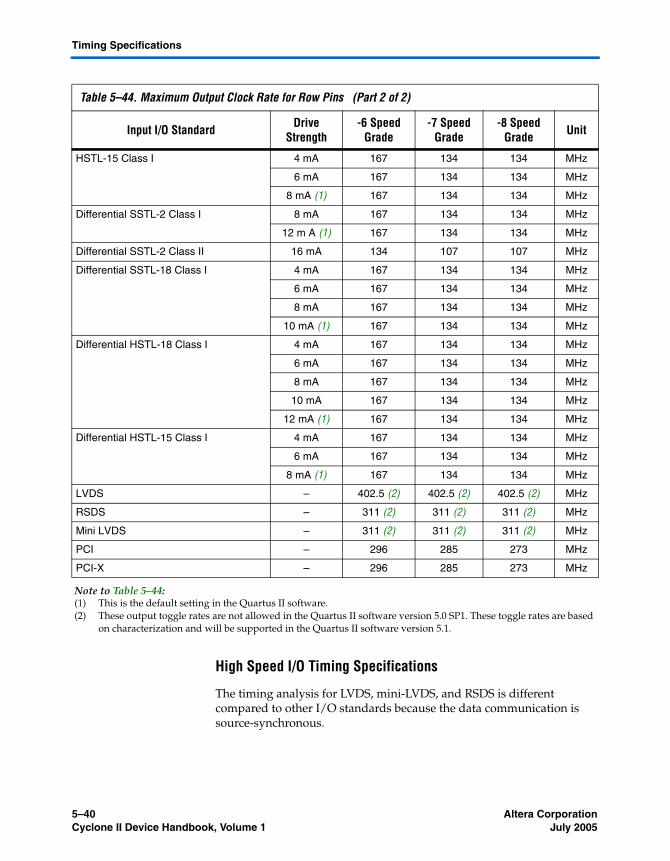
Timing Specifications
High Speed I/O Timing Specifications
The timing analysis for LVDS, mini-LVDS, and RSDS is different compared to other I/O standards because the data communication is source-synchronous.
HSTL-15 Class I 4 mA 167 134 134 MHz
6 mA 167 134 134 MHz
8 mA (1) 167 134 134 MHz
Differential SSTL-2 Class I 8 mA 167 134 134 MHz
12 m A (1) 167 134 134 MHz
Differential SSTL-2 Class II 16 mA 134 107 107 MHz
Differential SSTL-18 Class I 4 mA 167 134 134 MHz
6 mA 167 134 134 MHz
8 mA 167 134 134 MHz
10 mA (1) 167 134 134 MHz
Differential HSTL-18 Class I 4 mA 167 134 134 MHz
6 mA 167 134 134 MHz
8 mA 167 134 134 MHz
10 mA 167 134 134 MHz
12 mA (1) 167 134 134 MHz
Differential HSTL-15 Class I 4 mA 167 134 134 MHz
6 mA 167 134 134 MHz
8 mA (1) 167 134 134 MHz
LVDS – 402.5 (2) 402.5 (2) 402.5 (2) MHz
RSDS – 311 (2) 311 (2) 311 (2) MHz
Mini LVDS – 311 (2) 311 (2) 311 (2) MHz
PCI – 296 285 273 MHz
PCI-X – 296 285 273 MHz
Note to Table 5–44:(1) This is the default setting in the Quartus II software.(2) These output toggle rates are not allowed in the Quartus II software version 5.0 SP1. These toggle rates are based
on characterization and will be supported in the Quartus II software version 5.1.
Table 5–44. Maximum Output Clock Rate for Row Pins (Part 2 of 2)
Input I/O Standard Drive Strength
-6 Speed Grade
-7 Speed Grade
-8 Speed Grade Unit
5–40 Altera CorporationCyclone II Device Handbook, Volume 1 July 2005
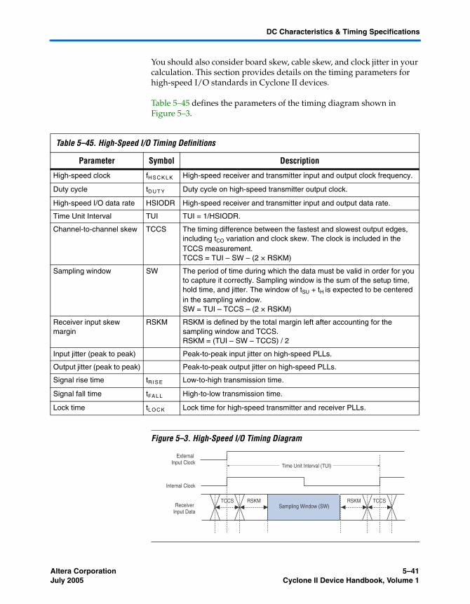
DC Characteristics & Timing Specifications
You should also consider board skew, cable skew, and clock jitter in your calculation. This section provides details on the timing parameters for high-speed I/O standards in Cyclone II devices.
Table 5–45 defines the parameters of the timing diagram shown in Figure 5–3.
Figure 5–3. High-Speed I/O Timing Diagram
Table 5–45. High-Speed I/O Timing Definitions
Parameter Symbol Description
High-speed clock fH S C K L K High-speed receiver and transmitter input and output clock frequency.
Duty cycle tD UT Y Duty cycle on high-speed transmitter output clock.
High-speed I/O data rate HSIODR High-speed receiver and transmitter input and output data rate.
Time Unit Interval TUI TUI = 1/HSIODR.
Channel-to-channel skew TCCS The timing difference between the fastest and slowest output edges, including tCO variation and clock skew. The clock is included in the TCCS measurement.TCCS = TUI – SW – (2 × RSKM)
Sampling window SW The period of time during which the data must be valid in order for you to capture it correctly. Sampling window is the sum of the setup time, hold time, and jitter. The window of tSU + tH is expected to be centered in the sampling window.SW = TUI – TCCS – (2 × RSKM)
Receiver input skew margin
RSKM RSKM is defined by the total margin left after accounting for the sampling window and TCCS. RSKM = (TUI – SW – TCCS) / 2
Input jitter (peak to peak) Peak-to-peak input jitter on high-speed PLLs.
Output jitter (peak to peak) Peak-to-peak output jitter on high-speed PLLs.
Signal rise time tR I S E Low-to-high transmission time.
Signal fall time tFA L L High-to-low transmission time.
Lock time tL O C K Lock time for high-speed transmitter and receiver PLLs.
Sampling Window (SW)
Time Unit Interval (TUI)
RSKM TCCSRSKMTCCS
Internal Clock
External Input Clock
Receiver Input Data
Altera Corporation 5–41July 2005 Cyclone II Device Handbook, Volume 1
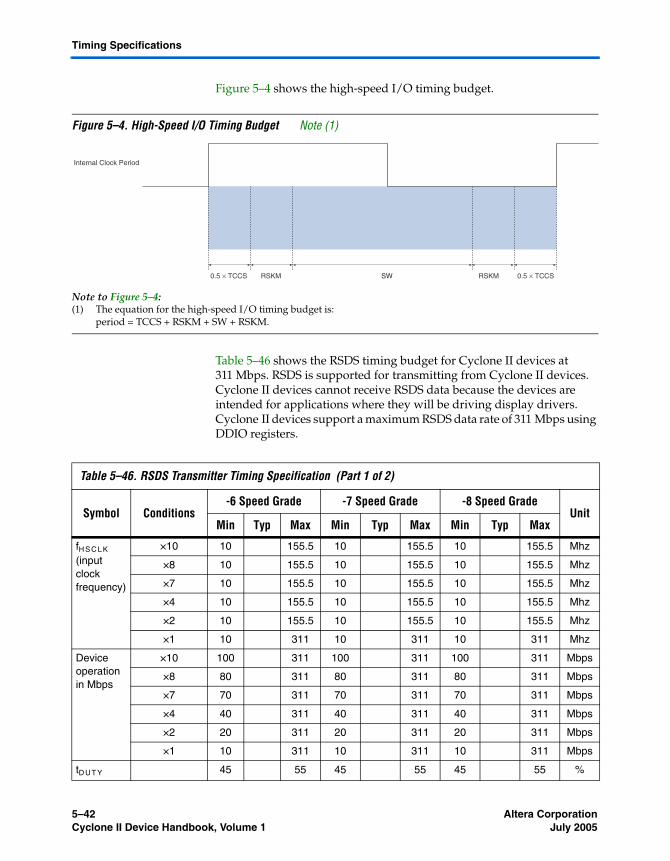
Timing Specifications
Figure 5–4 shows the high-speed I/O timing budget.
Figure 5–4. High-Speed I/O Timing Budget Note (1)
Note to Figure 5–4:(1) The equation for the high-speed I/O timing budget is:
period = TCCS + RSKM + SW + RSKM.
Table 5–46 shows the RSDS timing budget for Cyclone II devices at 311 Mbps. RSDS is supported for transmitting from Cyclone II devices. Cyclone II devices cannot receive RSDS data because the devices are intended for applications where they will be driving display drivers. Cyclone II devices support a maximum RSDS data rate of 311 Mbps using DDIO registers.
Internal Clock Period
RSKM 0.5 × TCCS RSKM 0.5 × TCCSSW
Table 5–46. RSDS Transmitter Timing Specification (Part 1 of 2)
Symbol Conditions-6 Speed Grade -7 Speed Grade -8 Speed Grade
UnitMin Typ Max Min Typ Max Min Typ Max
fH S C L K (input clock frequency)
×10 10 155.5 10 155.5 10 155.5 Mhz
×8 10 155.5 10 155.5 10 155.5 Mhz
×7 10 155.5 10 155.5 10 155.5 Mhz
×4 10 155.5 10 155.5 10 155.5 Mhz
×2 10 155.5 10 155.5 10 155.5 Mhz
×1 10 311 10 311 10 311 Mhz
Device operation in Mbps
×10 100 311 100 311 100 311 Mbps
×8 80 311 80 311 80 311 Mbps
×7 70 311 70 311 70 311 Mbps
×4 40 311 40 311 40 311 Mbps
×2 20 311 20 311 20 311 Mbps
×1 10 311 10 311 10 311 Mbps
tD UT Y 45 55 45 55 45 55 %
5–42 Altera CorporationCyclone II Device Handbook, Volume 1 July 2005
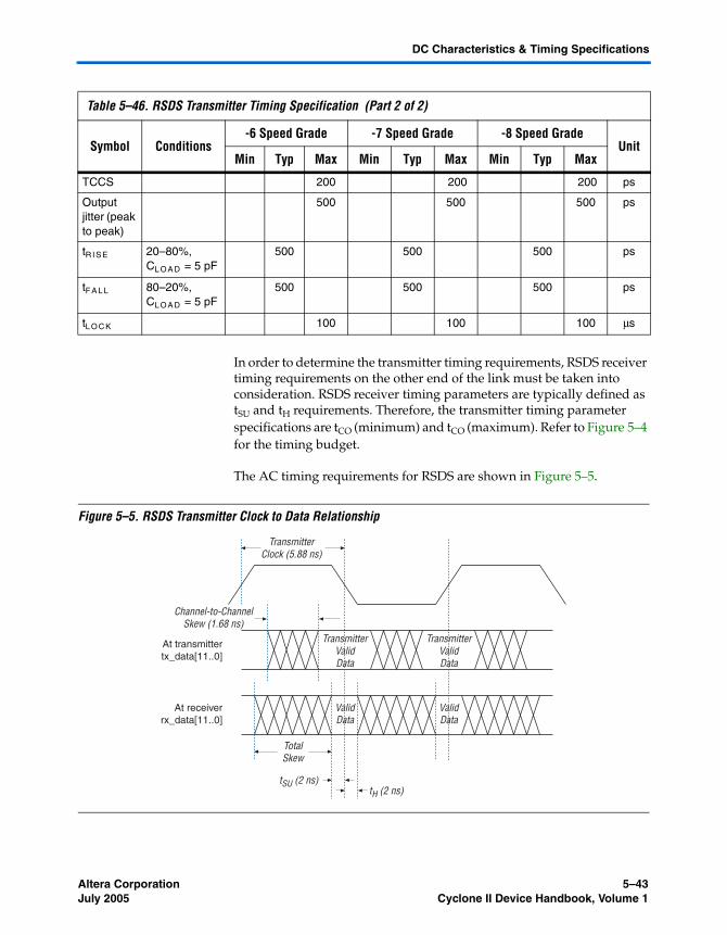
DC Characteristics & Timing Specifications
In order to determine the transmitter timing requirements, RSDS receiver timing requirements on the other end of the link must be taken into consideration. RSDS receiver timing parameters are typically defined as tSU and tH requirements. Therefore, the transmitter timing parameter specifications are tCO (minimum) and tCO (maximum). Refer to Figure 5–4 for the timing budget.
The AC timing requirements for RSDS are shown in Figure 5–5.
Figure 5–5. RSDS Transmitter Clock to Data Relationship
TCCS 200 200 200 ps
Output jitter (peak to peak)
500 500 500 ps
tR I S E 20–80%, CL O A D = 5 pF
500 500 500 ps
tF A L L 80–20%, CL O A D = 5 pF
500 500 500 ps
tL O C K 100 100 100 μs
Table 5–46. RSDS Transmitter Timing Specification (Part 2 of 2)
Symbol Conditions-6 Speed Grade -7 Speed Grade -8 Speed Grade
UnitMin Typ Max Min Typ Max Min Typ Max
TransmitterValidData
TransmitterValidData
ValidData
TotalSkew
ValidData
tSU (2 ns)tH (2 ns)
Channel-to-ChannelSkew (1.68 ns)
TransmitterClock (5.88 ns)
At transmittertx_data[11..0]
At receiverrx_data[11..0]
Altera Corporation 5–43July 2005 Cyclone II Device Handbook, Volume 1
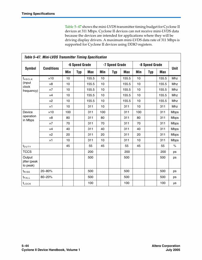
Timing Specifications
Table 5–47 shows the mini-LVDS transmitter timing budget for Cyclone II devices at 311 Mbps. Cyclone II devices can not receive mini-LVDS data because the devices are intended for applications where they will be driving display drivers. A maximum mini-LVDS data rate of 311 Mbps is supported for Cyclone II devices using DDIO registers.
Table 5–47. Mini-LVDS Transmitter Timing Specification
Symbol Conditions-6 Speed Grade -7 Speed Grade -8 Speed Grade
UnitMin Typ Max Min Typ Max Min Typ Max
fH S C L K (input clock frequency)
×10 10 155.5 10 155.5 10 155.5 Mhz
×8 10 155.5 10 155.5 10 155.5 Mhz
×7 10 155.5 10 155.5 10 155.5 Mhz
×4 10 155.5 10 155.5 10 155.5 Mhz
×2 10 155.5 10 155.5 10 155.5 Mhz
×1 10 311 10 311 10 311 Mhz
Device operation in Mbps
×10 100 311 100 311 100 311 Mbps
×8 80 311 80 311 80 311 Mbps
×7 70 311 70 311 70 311 Mbps
×4 40 311 40 311 40 311 Mbps
×2 20 311 20 311 20 311 Mbps
×1 10 311 10 311 10 311 Mbps
tD UT Y 45 55 45 55 45 55 %
TCCS 200 200 200 ps
Output jitter (peak to peak)
500 500 500 ps
tR I S E 20–80% 500 500 500 ps
tF A L L 80–20% 500 500 500 ps
tL O C K 100 100 100 μs
5–44 Altera CorporationCyclone II Device Handbook, Volume 1 July 2005
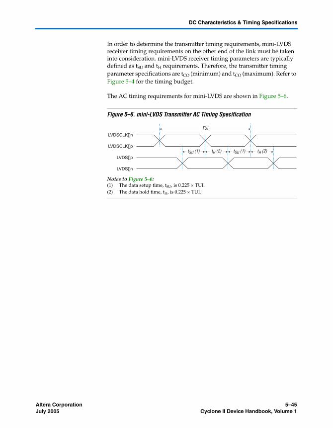
DC Characteristics & Timing Specifications
In order to determine the transmitter timing requirements, mini-LVDS receiver timing requirements on the other end of the link must be taken into consideration. mini-LVDS receiver timing parameters are typically defined as tSU and tH requirements. Therefore, the transmitter timing parameter specifications are tCO (minimum) and tCO (maximum). Refer to Figure 5–4 for the timing budget.
The AC timing requirements for mini-LVDS are shown in Figure 5–6.
Figure 5–6. mini-LVDS Transmitter AC Timing Specification
Notes to Figure 5–6:(1) The data setup time, tSU, is 0.225 × TUI.(2) The data hold time, tH, is 0.225 × TUI.
tSU (1) tH (2)
TUI
tSU (1) tH (2)
LVDSCLK[]n
LVDSCLK[]p
LVDS[]p
LVDS[]n
Altera Corporation 5–45July 2005 Cyclone II Device Handbook, Volume 1
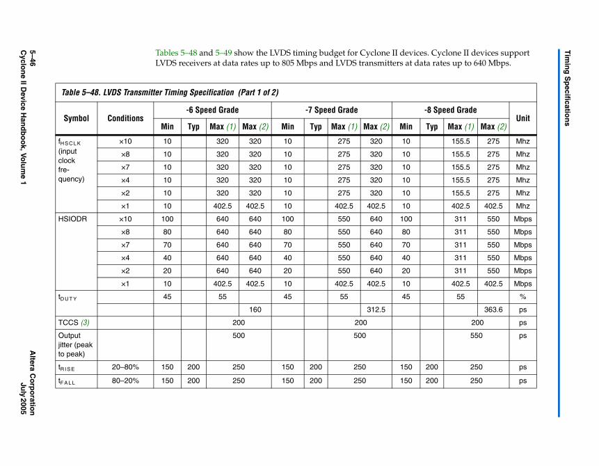
5–46
Altera C
orp
oratio
nC
yclon
e II Device H
and
bo
ok, Vo
lum
e 1
July 2005
Tim
ing
Sp
ecification
s
. Cyclone II devices support a rates up to 640 Mbps.
8 Speed GradeUnit
Typ Max (1) Max (2)
155.5 275 Mhz
155.5 275 Mhz
155.5 275 Mhz
155.5 275 Mhz
155.5 275 Mhz
402.5 402.5 Mhz
311 550 Mbps
311 550 Mbps
311 550 Mbps
311 550 Mbps
311 550 Mbps
402.5 402.5 Mbps
55 %
363.6 ps
200 ps
550 ps
200 250 ps
200 250 ps
Tables 5–48 and 5–49 show the LVDS timing budget for Cyclone II devicesLVDS receivers at data rates up to 805 Mbps and LVDS transmitters at dat
Table 5–48. LVDS Transmitter Timing Specification (Part 1 of 2)
Symbol Conditions-6 Speed Grade -7 Speed Grade -
Min Typ Max (1) Max (2) Min Typ Max (1) Max (2) Min
fH S C L K (input clockfre-quency)
×10 10 320 320 10 275 320 10
×8 10 320 320 10 275 320 10
×7 10 320 320 10 275 320 10
×4 10 320 320 10 275 320 10
×2 10 320 320 10 275 320 10
×1 10 402.5 402.5 10 402.5 402.5 10
HSIODR ×10 100 640 640 100 550 640 100
×8 80 640 640 80 550 640 80
×7 70 640 640 70 550 640 70
×4 40 640 640 40 550 640 40
×2 20 640 640 20 550 640 20
×1 10 402.5 402.5 10 402.5 402.5 10
tD UT Y 45 55 45 55 45
160 312.5
TCCS (3) 200 200
Output jitter (peak to peak)
500 500
tR I S E 20–80% 150 200 250 150 200 250 150
tF A L L 80–20% 150 200 250 150 200 250 150
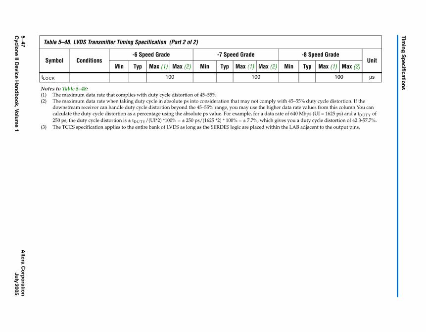
5–47
Altera C
orp
oratio
nC
yclon
e II Device H
and
bo
ok, Vo
lum
e 1
July 2005
Tim
ing
Sp
ecification
s
100 μs
duty cycle distortion. If the values from this column.You can bps (UI = 1625 ps) and a tD U T Y of uty cycle distortion of 42.3-57.7%.djacent to the output pins.
8 Speed GradeUnit
Typ Max (1) Max (2)
tL O C K 100 100
Notes to Table 5–48:(1) The maximum data rate that complies with duty cycle distortion of 45–55%.(2) The maximum data rate when taking duty cycle in absolute ps into consideration that may not comply with 45–55%
downstream receiver can handle duty cycle distortion beyond the 45–55% range, you may use the higher data rate calculate the duty cycle distortion as a percentage using the absolute ps value. For example, for a data rate of 640 M250 ps, the duty cycle distortion is ± tD U T Y/(UI*2) *100% = ± 250 ps/(1625 *2) * 100% = ± 7.7%, which gives you a d
(3) The TCCS specification applies to the entire bank of LVDS as long as the SERDES logic are placed within the LAB a
Table 5–48. LVDS Transmitter Timing Specification (Part 2 of 2)
Symbol Conditions-6 Speed Grade -7 Speed Grade -
Min Typ Max (1) Max (2) Min Typ Max (1) Max (2) Min
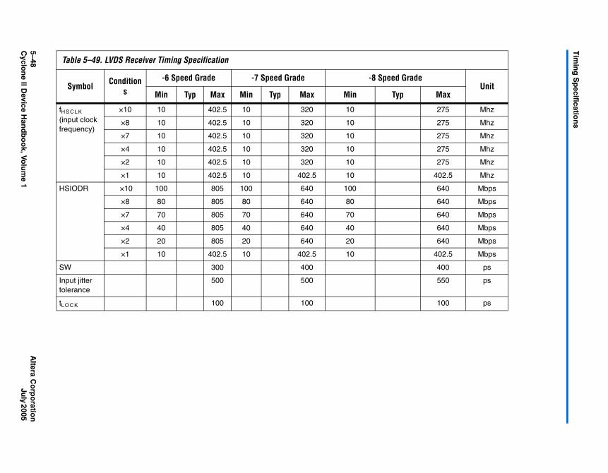
5–48
Altera C
orp
oratio
nC
yclon
e II Device H
and
bo
ok, Vo
lum
e 1
July 2005
Tim
ing
Sp
ecification
s
UnitMax
275 Mhz
275 Mhz
275 Mhz
275 Mhz
275 Mhz
402.5 Mhz
640 Mbps
640 Mbps
640 Mbps
640 Mbps
640 Mbps
402.5 Mbps
400 ps
550 ps
100 ps
Table 5–49. LVDS Receiver Timing Specification
Symbol Conditions
-6 Speed Grade -7 Speed Grade -8 Speed Grade
Min Typ Max Min Typ Max Min Typ
fH S C L K (input clock frequency)
×10 10 402.5 10 320 10
×8 10 402.5 10 320 10
×7 10 402.5 10 320 10
×4 10 402.5 10 320 10
×2 10 402.5 10 320 10
×1 10 402.5 10 402.5 10
HSIODR ×10 100 805 100 640 100
×8 80 805 80 640 80
×7 70 805 70 640 70
×4 40 805 40 640 40
×2 20 805 20 640 20
×1 10 402.5 10 402.5 10
SW 300 400
Input jitter tolerance
500 500
tL O C K 100 100
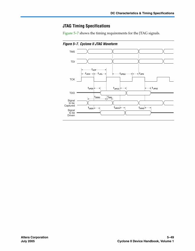
DC Characteristics & Timing Specifications
JTAG Timing Specifications
Figure 5–7 shows the timing requirements for the JTAG signals.
Figure 5–7. Cyclone II JTAG Waveform
TDO
TCK
tJPZX tJPCO
tJPH
t JPXZ
tJCP
tJPSU t JCL tJCH
TDI
TMS
Signalto be
Captured
Signalto be
Driven
tJSZX
tJSSU tJSH
tJSCO tJSXZ
Altera Corporation 5–49July 2005 Cyclone II Device Handbook, Volume 1
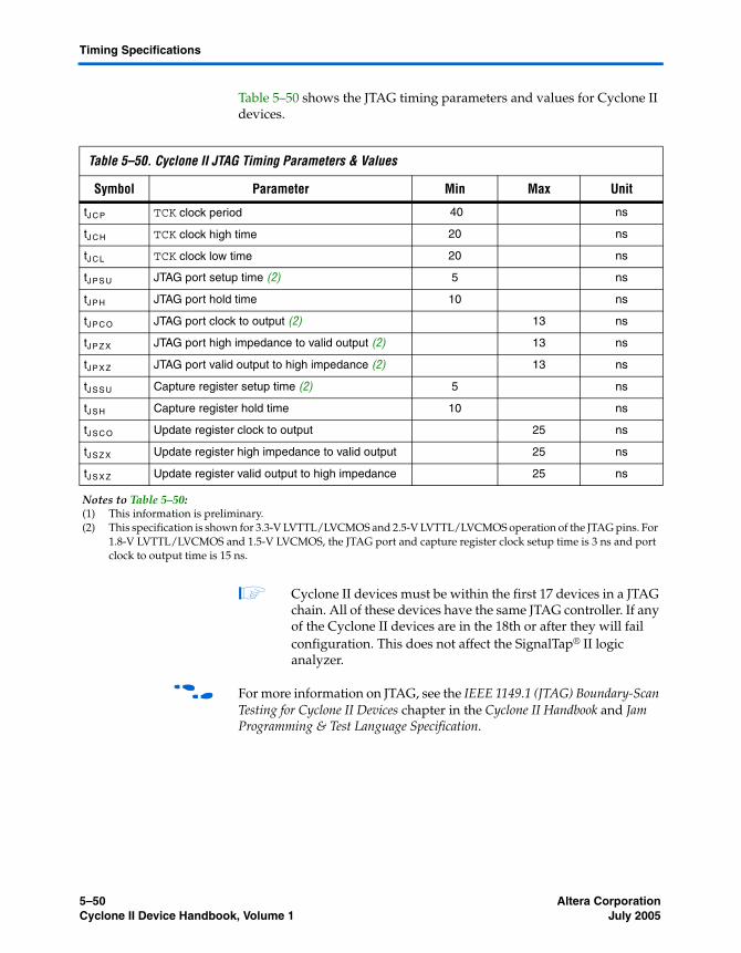
Timing Specifications
Table 5–50 shows the JTAG timing parameters and values for Cyclone II devices.
1 Cyclone II devices must be within the first 17 devices in a JTAG chain. All of these devices have the same JTAG controller. If any of the Cyclone II devices are in the 18th or after they will fail configuration. This does not affect the SignalTap® II logic analyzer.
f For more information on JTAG, see the IEEE 1149.1 (JTAG) Boundary-Scan Testing for Cyclone II Devices chapter in the Cyclone II Handbook and Jam Programming & Test Language Specification.
Table 5–50. Cyclone II JTAG Timing Parameters & Values
Symbol Parameter Min Max Unit
tJ C P TCK clock period 40 ns
tJ C H TCK clock high time 20 ns
tJ C L TCK clock low time 20 ns
tJ P S U JTAG port setup time (2) 5 ns
tJ P H JTAG port hold time 10 ns
tJ P C O JTAG port clock to output (2) 13 ns
tJ P Z X JTAG port high impedance to valid output (2) 13 ns
tJ P X Z JTAG port valid output to high impedance (2) 13 ns
tJ S S U Capture register setup time (2) 5 ns
tJ S H Capture register hold time 10 ns
tJ S C O Update register clock to output 25 ns
tJ S Z X Update register high impedance to valid output 25 ns
tJ S X Z Update register valid output to high impedance 25 ns
Notes to Table 5–50:(1) This information is preliminary.(2) This specification is shown for 3.3-V LVTTL/LVCMOS and 2.5-V LVTTL/LVCMOS operation of the JTAG pins. For
1.8-V LVTTL/LVCMOS and 1.5-V LVCMOS, the JTAG port and capture register clock setup time is 3 ns and port clock to output time is 15 ns.
5–50 Altera CorporationCyclone II Device Handbook, Volume 1 July 2005
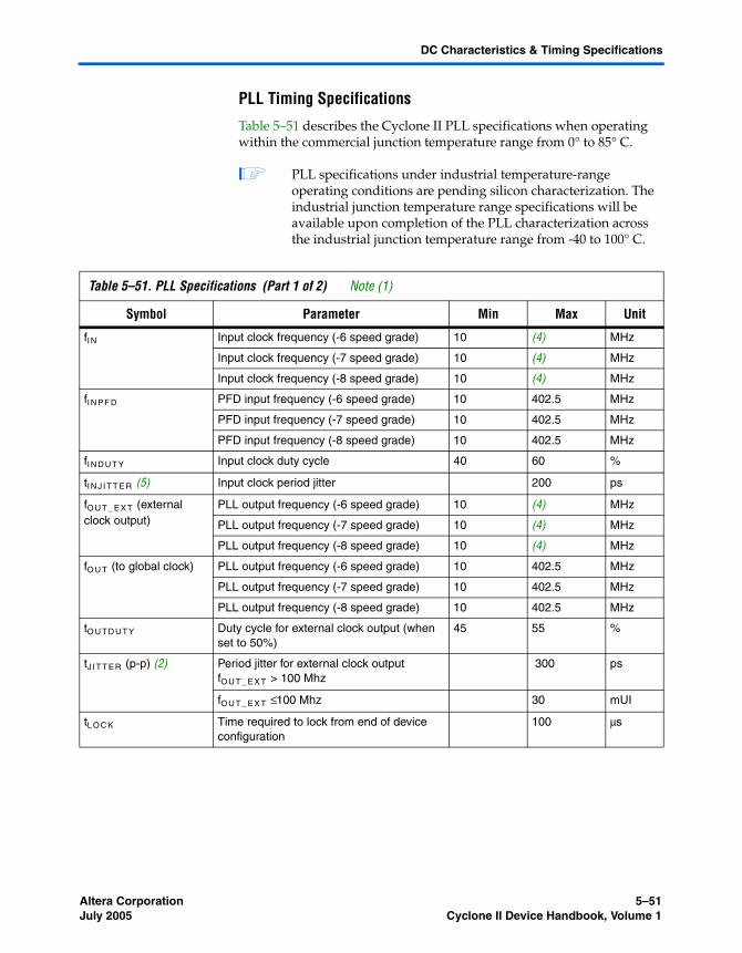
DC Characteristics & Timing Specifications
PLL Timing Specifications
Table 5–51 describes the Cyclone II PLL specifications when operating within the commercial junction temperature range from 0° to 85° C.
1 PLL specifications under industrial temperature-range operating conditions are pending silicon characterization. The industrial junction temperature range specifications will be available upon completion of the PLL characterization across the industrial junction temperature range from -40 to 100° C.
Table 5–51. PLL Specifications (Part 1 of 2) Note (1)
Symbol Parameter Min Max Unit
fI N Input clock frequency (-6 speed grade) 10 (4) MHz
Input clock frequency (-7 speed grade) 10 (4) MHz
Input clock frequency (-8 speed grade) 10 (4) MHz
fI N P F D PFD input frequency (-6 speed grade) 10 402.5 MHz
PFD input frequency (-7 speed grade) 10 402.5 MHz
PFD input frequency (-8 speed grade) 10 402.5 MHz
fI N D UT Y Input clock duty cycle 40 60 %
tI N J I T T E R (5) Input clock period jitter 200 ps
fO U T _ E X T (external clock output)
PLL output frequency (-6 speed grade) 10 (4) MHz
PLL output frequency (-7 speed grade) 10 (4) MHz
PLL output frequency (-8 speed grade) 10 (4) MHz
fO U T (to global clock) PLL output frequency (-6 speed grade) 10 402.5 MHz
PLL output frequency (-7 speed grade) 10 402.5 MHz
PLL output frequency (-8 speed grade) 10 402.5 MHz
tO U T D UT Y Duty cycle for external clock output (when set to 50%)
45 55 %
tJ I T T E R (p-p) (2) Period jitter for external clock output fO UT _ E X T > 100 Mhz
300 ps
fO UT _ E X T ≤ 100 Mhz 30 mUI
tL O C K Time required to lock from end of device configuration
100 μs
Altera Corporation 5–51July 2005 Cyclone II Device Handbook, Volume 1
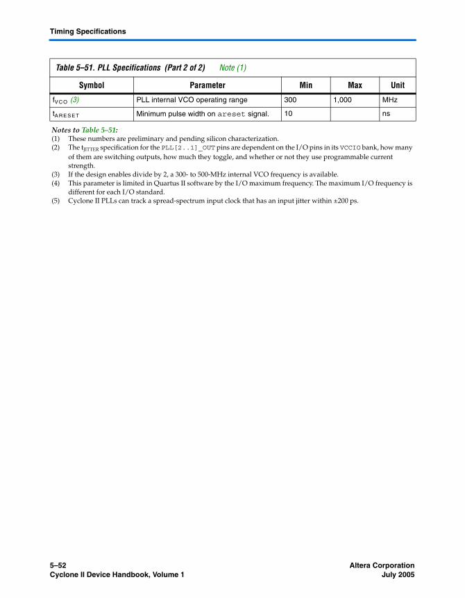
Timing Specifications
fV C O (3) PLL internal VCO operating range 300 1,000 MHz
tA R E S E T Minimum pulse width on areset signal. 10 ns
Notes to Table 5–51:(1) These numbers are preliminary and pending silicon characterization.(2) The tJITTER specification for the PLL[2..1]_OUT pins are dependent on the I/O pins in its VCCIO bank, how many
of them are switching outputs, how much they toggle, and whether or not they use programmable current strength.
(3) If the design enables divide by 2, a 300- to 500-MHz internal VCO frequency is available.(4) This parameter is limited in Quartus II software by the I/O maximum frequency. The maximum I/O frequency is
different for each I/O standard.(5) Cyclone II PLLs can track a spread-spectrum input clock that has an input jitter within ±200 ps.
Table 5–51. PLL Specifications (Part 2 of 2) Note (1)
Symbol Parameter Min Max Unit
5–52 Altera CorporationCyclone II Device Handbook, Volume 1 July 2005
Altera Corporation November 2004
CII51006-1.1
6. Reference & OrderingInformation
Software CycloneTM II devices are supported by the Altera® Quartus® II design software, which provides a comprehensive environment for system-on-a-programmable-chip (SOPC) design. The Quartus II software includes HDL and schematic design entry, compilation and logic synthesis, full simulation and advanced timing analysis, SignalTap® II logic analyzer, and device configuration. See the Quartus II Handbook for more information on the Quartus II software features.
The Quartus II software supports the Windows XP/2000/NT/98, Sun Solaris, Linux Red Hat v7.1 and HP-UX operating systems. It also supports seamless integration with industry-leading EDA tools through the NativeLink® interface.
Device Pin-Outs Device pin-outs for Cyclone II devices are available on the Altera web site (www.altera.com). For more information contact Altera Applications.
Ordering Information
Figure 6–1 describes the ordering codes for Cyclone II devices. For more information on a specific package, contact Altera Applications.
6–1Preliminary
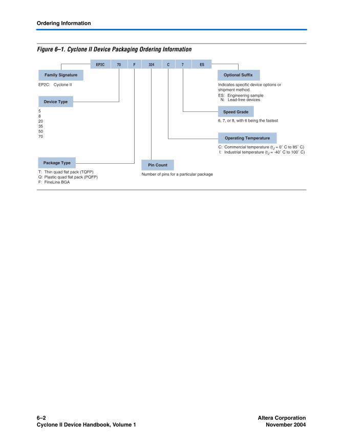
Ordering Information
Figure 6–1. Cyclone II Device Packaging Ordering Information
Device Type
Package Type
6, 7, or 8, with 6 being the fastest
Number of pins for a particular package
ES:
T:Q:F:
Thin quad flat pack (TQFP)Plastic quad flat pack (PQFP)FineLine BGA
EP2C: Cyclone II
5820355070
C: Commercial temperature (tJ = 0˚ C to 85˚ C)Industrial temperature (tJ = -40˚ C to 100˚ C)
Optional SuffixFamily Signature
Operating Temperature
Speed Grade
Pin Count
Engineering sample
7EP2C 70 C324F ES
Indicates specific device options or shipment method.
N: Lead-free devices
I:
6–2 Altera CorporationCyclone II Device Handbook, Volume 1 November 2004