Cyclone Handbook Volume 1, Chapter 8. Using Selectable … · Altera Corporation 8–1 ... 8. Using...
24
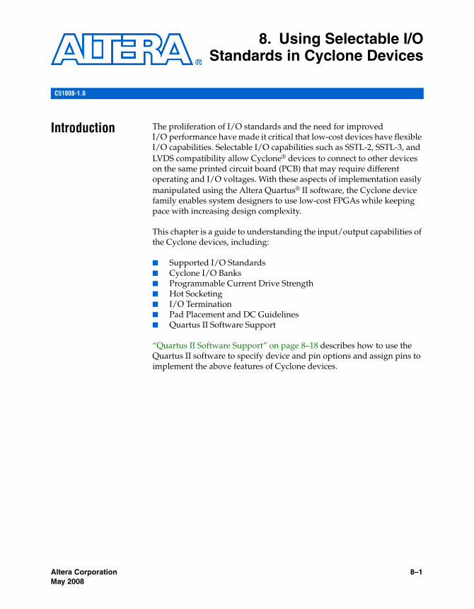
Altera Corporation 8–1 May 2008 Preliminary 8. Using Selectable I/O Standards in Cyclone Devices Introduction The proliferation of I/O standards and the need for improved I/O performance have made it critical that low-cost devices have flexible I/O capabilities. Selectable I/O capabilities such as SSTL-2, SSTL-3, and LVDS compatibility allow Cyclone ® devices to connect to other devices on the same printed circuit board (PCB) that may require different operating and I/O voltages. With these aspects of implementation easily manipulated using the Altera Quartus ® II software, the Cyclone device family enables system designers to use low-cost FPGAs while keeping pace with increasing design complexity. This chapter is a guide to understanding the input/output capabilities of the Cyclone devices, including: ■ Supported I/O Standards ■ Cyclone I/O Banks ■ Programmable Current Drive Strength ■ Hot Socketing ■ I/O Termination ■ Pad Placement and DC Guidelines ■ Quartus II Software Support “Quartus II Software Support” on page 8–18 describes how to use the Quartus II software to specify device and pin options and assign pins to implement the above features of Cyclone devices. C51008-1.6
Transcript of Cyclone Handbook Volume 1, Chapter 8. Using Selectable … · Altera Corporation 8–1 ... 8. Using...
Altera Corporation 8–1May 2008 Preliminary
8. Using Selectable I/OStandards in Cyclone Devices
Introduction The proliferation of I/O standards and the need for improved I/O performance have made it critical that low-cost devices have flexible I/O capabilities. Selectable I/O capabilities such as SSTL-2, SSTL-3, and LVDS compatibility allow Cyclone® devices to connect to other devices on the same printed circuit board (PCB) that may require different operating and I/O voltages. With these aspects of implementation easily manipulated using the Altera Quartus® II software, the Cyclone device family enables system designers to use low-cost FPGAs while keeping pace with increasing design complexity.
This chapter is a guide to understanding the input/output capabilities of the Cyclone devices, including:
■ Supported I/O Standards■ Cyclone I/O Banks■ Programmable Current Drive Strength■ Hot Socketing■ I/O Termination■ Pad Placement and DC Guidelines■ Quartus II Software Support
“Quartus II Software Support” on page 8–18 describes how to use the Quartus II software to specify device and pin options and assign pins to implement the above features of Cyclone devices.
C51008-1.6
8–2 Altera CorporationPreliminary May 2008
Cyclone Device Handbook, Volume 1
Supported I/O Standards
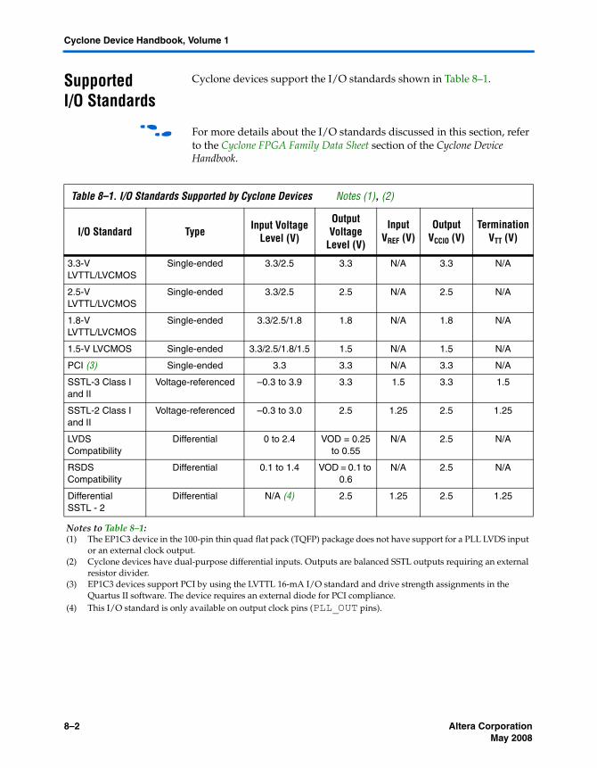
Cyclone devices support the I/O standards shown in Table 8–1.
f For more details about the I/O standards discussed in this section, refer to the Cyclone FPGA Family Data Sheet section of the Cyclone Device Handbook.
Table 8–1. I/O Standards Supported by Cyclone Devices Notes (1), (2)
I/O Standard Type Input Voltage Level (V)
Output Voltage
Level (V)
Input VREF (V)
Output VCCIO (V)
Termination VTT (V)
3.3-V LVTTL/LVCMOS
Single-ended 3.3/2.5 3.3 N/A 3.3 N/A
2.5-V LVTTL/LVCMOS
Single-ended 3.3/2.5 2.5 N/A 2.5 N/A
1.8-V LVTTL/LVCMOS
Single-ended 3.3/2.5/1.8 1.8 N/A 1.8 N/A
1.5-V LVCMOS Single-ended 3.3/2.5/1.8/1.5 1.5 N/A 1.5 N/A
PCI (3) Single-ended 3.3 3.3 N/A 3.3 N/A
SSTL-3 Class I and II
Voltage-referenced –0.3 to 3.9 3.3 1.5 3.3 1.5
SSTL-2 Class I and II
Voltage-referenced –0.3 to 3.0 2.5 1.25 2.5 1.25
LVDS Compatibility
Differential 0 to 2.4 VOD = 0.25 to 0.55
N/A 2.5 N/A
RSDS Compatibility
Differential 0.1 to 1.4 VOD = 0.1 to 0.6
N/A 2.5 N/A
Differential SSTL - 2
Differential N/A (4) 2.5 1.25 2.5 1.25
Notes to Table 8–1:(1) The EP1C3 device in the 100-pin thin quad flat pack (TQFP) package does not have support for a PLL LVDS input
or an external clock output.(2) Cyclone devices have dual-purpose differential inputs. Outputs are balanced SSTL outputs requiring an external
resistor divider.(3) EP1C3 devices support PCI by using the LVTTL 16-mA I/O standard and drive strength assignments in the
Quartus II software. The device requires an external diode for PCI compliance.(4) This I/O standard is only available on output clock pins (PLL_OUT pins).
Altera Corporation 8–3May 2008 Preliminary
Supported I/O Standards
3.3-V LVTTL (EIA/JEDEC Standard JESD8-B)
The 3.3-V LVTTL I/O standard is a general-purpose, single-ended standard used for 3.3-V applications. The LVTTL standard defines the DC interface parameters for digital circuits operating from a 3.0-V/3.3-V power supply and driving or being driven by LVTTL-compatible devices.
The LVTTL input standard specifies a wider input voltage range of – 0.3 V ≤VI ≤ 3.9 V. Altera recommends an input voltage range of – 0.5 V ≤ VI ≤ 4.1 V. The LVTTL standard does not require input reference voltages or board terminations. Cyclone devices support both input and output levels for 3.3-V LVTTL.
3.3-V LVCMOS (EIA/JEDEC Standard JESD8-B)
The 3.3-V LVCMOS I/O standard is a general-purpose, single-ended standard used for 3.3-V applications. The LVCMOS standard defines the DC interface parameters for digital circuits operating from a 3.0-V or 3.3-V power supply and driving or being driven by LVCMOS-compatible devices.
The LVCMOS standard specifies the same input voltage requirements as LVTTL (– 0.3 V ≤ VI ≤ 3.9 V). The output buffer drives to the rail to meet the minimum high-level output voltage requirements. The 3.3-V I/O Standard does not require input reference voltages or board terminations. Cyclone devices support both input and output levels specified by the 3.3-V LVCMOS I/O standard.
2.5-V LVTTL Normal and Wide Voltage Ranges (EIA/JEDEC Standard EIA/JESD8-5)
The 2.5-V I/O standard is used for 2.5-V LVTTL applications. This standard defines the DC interface parameters for high-speed, low-voltage, non-terminated digital circuits driving or being driven by other 2.5-V devices. The input and output voltage requirements are:
■ The 2.5-V normal and wide range input standards specify an input voltage range of –0.3 V ≤ VI ≤ 3.0-V.
■ The normal range minimum high-level output voltage requirement (VOH) is 2.1-V.
■ The wide range minimum high-level output voltage requirement (VOH) is VCCIO – 0.2-V.
The 2.5-V standard does not require input reference voltages or board terminations. Cyclone devices support input and output levels for both 2.5-V LVTTL ranges.
8–4 Altera CorporationPreliminary May 2008
Cyclone Device Handbook, Volume 1
2.5-V LVCMOS Normal and Wide Voltage Ranges (EIA/JEDEC Standard EIA/JESD8-5)
The 2.5-V I/O standard is used for 2.5-V LVCMOS applications. This standard defines the DC interface parameters for high-speed, low-voltage, non-terminated digital circuits driving or being driven by other 2.5-V parts. The input and output voltage ranges are:
■ The 2.5-V normal and wide range input standards specify an input voltage range of – 0.3-V ≤ VI ≤ 3.0-V.
■ The normal range minimum VOH requirement is 2.1 V.■ The wide range minimum VOH requirement is VCCIO – 0.2 V.
The 2.5-V standard does not require input reference voltages or board terminations. Cyclone devices support input and output levels for both 2.5-V LVCMOS ranges.
1.8-V LVTTL Normal and Wide Voltage Ranges (EIA/JEDEC Standard EIA/JESD8-7)
The 1.8-V I/O standard is used for 1.8-V LVTTL applications. This standard defines the DC interface parameters for high-speed, low-voltage, non-terminated digital circuits driving or being driven by other 1.8-V parts. The input and output voltage ranges are:
■ The 1.8-V normal and wide range input standards specify an input voltage range of – 0.3 V ≤ VI ≤ 2.25 V.
■ The normal range minimum VOH requirement is VCCIO – 0.45 V.■ The wide range minimum VOH requirement is VCCIO – 0.2 V.
The 1.8-V standard does not require input reference voltages or board terminations. Cyclone devices support input and output levels for both normal and wide 1.8-V LVTTL ranges.
1.8-V LVCMOS Normal and Wide Voltage Ranges (EIA/JEDEC Standard EIA/JESD8-7)
The 1.8-V I/O standard is used for 1.8-V LVCMOS applications. This standard defines the DC interface parameters for high-speed, low-voltage, non-terminated digital circuits driving or being driven by other 1.8-V devices. The input and output voltage ranges are:
■ The 1.8-V normal and wide range input standards specify an input voltage range of – 0.3 V ≤ VI ≤ 2.25 V.
■ The normal range minimum VOH requirement is VCCIO – 0.45 V.■ The wide range minimum VOH requirement is VCCIO – 0.2 V.
Altera Corporation 8–5May 2008 Preliminary
Supported I/O Standards
The 1.8-V standard does not require input reference voltages or board terminations. Cyclone devices support input and output levels for both normal and wide 1.8-V LVCMOS ranges.
1.5-V LVCMOS Normal and Wide Voltage Ranges (EIA/JEDEC Standard JESD8-11)
The 1.5-V I/O standard is used for 1.5-V applications. This standard defines the DC interface parameters for high-speed, low-voltage, non-terminated digital circuits driving or being driven by other 1.5-V devices. The input and output voltage ranges are:
■ The 1.5-V normal and wide range input standards specify an input voltage range of – 0.3 V ≤ VI ≤ 1.9-V.
■ The normal range minimum VOH requirement is 1.05 V.■ The wide range minimum VOH requirement is VCCIO – 0.2-V.
The 1.5-V standard does not require input reference voltages or board terminations. Cyclone devices support input and output levels for both normal and wide 1.5-V LVCMOS ranges.
3.3-V (PCI Special Interest Group (SIG) PCI Local Bus Specification Revision 2.2)
The PCI local bus specification is used for applications that interface to the PCI local bus, which provides a processor-independent data path between highly integrated peripheral controller components, peripheral add-in boards, and processor/memory systems. The conventional PCI specification revision 2.2 defines the PCI hardware environment including the protocol, electrical, mechanical, and configuration specifications for the PCI devices and expansion boards. This standard requires 3.3-V VCCIO. The 3.3-V PCI standard does not require input reference voltages or board terminations.
The side I/O pins on all Cyclone devices (except the EP1C3 device) are fully compliant with the 3.3-V PCI Local Bus Specification Revision 2.2 and meet 32-bit/66-MHz operating frequency and timing requirements. The EP1C3 device supports the PCI I/O standard by using the LVTTL 16-mA setting and an external diode. The top and bottom I/O pins on all Cylcone devices support PCI by using the LVTTL 16-mA setting and an external diode.
Cyclone devices support PCI input and output levels on I/O banks 1 and 3 only. See “Cyclone I/O Banks” for more details and the IP MegaStoreTM website.
8–6 Altera CorporationPreliminary May 2008
Cyclone Device Handbook, Volume 1
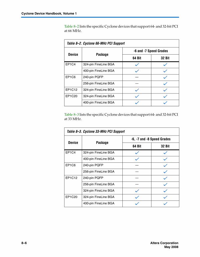
Table 8–2 lists the specific Cyclone devices that support 64- and 32-bit PCI at 66 MHz.
Table 8–3 lists the specific Cyclone devices that support 64- and 32-bit PCI at 33 MHz.
Table 8–2. Cyclone 66-MHz PCI Support
Device Package-6 and -7 Speed Grades
64 Bit 32 Bit
EP1C4 324-pin FineLine BGA v v
400-pin FineLine BGA v v
EP1C6 240-pin PQFP — v
256-pin FineLine BGA — v
EP1C12 324-pin FineLine BGA v v
EP1C20 324-pin FineLine BGA v v
400-pin FineLine BGA v v
Table 8–3. Cyclone 33-MHz PCI Support
Device Package-6, -7 and -8 Speed Grades
64 Bit 32 Bit
EP1C4 324-pin FineLine BGA v v
400-pin FineLine BGA v v
EP1C6 240-pin PQFP — v
256-pin FineLine BGA — v
EP1C12 240-pin PQFP — v
256-pin FineLine BGA — v
324-pin FineLine BGA v v
EP1C20 324-pin FineLine BGA v v
400-pin FineLine BGA v v
Altera Corporation 8–7May 2008 Preliminary
Supported I/O Standards
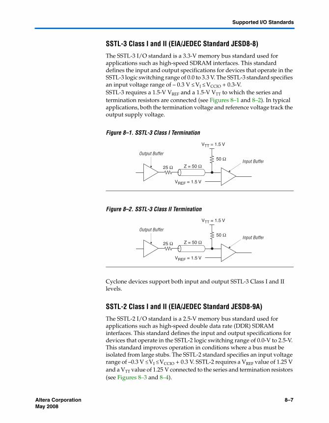
SSTL-3 Class I and II (EIA/JEDEC Standard JESD8-8)
The SSTL-3 I/O standard is a 3.3-V memory bus standard used for applications such as high-speed SDRAM interfaces. This standard defines the input and output specifications for devices that operate in the SSTL-3 logic switching range of 0.0 to 3.3 V. The SSTL-3 standard specifies an input voltage range of – 0.3 V ≤ VI ≤ VCCIO + 0.3-V.SSTL-3 requires a 1.5-V VREF and a 1.5-V VTT to which the series and termination resistors are connected (see Figures 8–1 and 8–2). In typical applications, both the termination voltage and reference voltage track the output supply voltage.
Figure 8–1. SSTL-3 Class I Termination
Figure 8–2. SSTL-3 Class II Termination
Cyclone devices support both input and output SSTL-3 Class I and II levels.
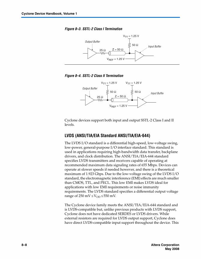
SSTL-2 Class I and II (EIA/JEDEC Standard JESD8-9A)
The SSTL-2 I/O standard is a 2.5-V memory bus standard used for applications such as high-speed double data rate (DDR) SDRAM interfaces. This standard defines the input and output specifications for devices that operate in the SSTL-2 logic switching range of 0.0-V to 2.5-V. This standard improves operation in conditions where a bus must be isolated from large stubs. The SSTL-2 standard specifies an input voltage range of –0.3 V ≤ VI ≤ VCCIO + 0.3 V. SSTL-2 requires a VREF value of 1.25 V and a VTT value of 1.25 V connected to the series and termination resistors (see Figures 8–3 and 8–4).
Output Buffer
Input Buffer
VTT = 1.5 V
50 Ω
25 Ω Z = 50 Ω
VREF = 1.5 V
Output Buffer
Input Buffer
VTT = 1.5 V
50 Ω
25 Ω Z = 50 Ω
VREF = 1.5 V
8–8 Altera CorporationPreliminary May 2008
Cyclone Device Handbook, Volume 1
Figure 8–3. SSTL-2 Class I Termination
Figure 8–4. SSTL-2 Class II Termination
Cyclone devices support both input and output SSTL-2 Class I and II levels.
LVDS (ANSI/TIA/EIA Standard ANSI/TIA/EIA-644)
The LVDS I/O standard is a differential high-speed, low-voltage swing, low-power, general-purpose I/O interface standard. This standard is used in applications requiring high-bandwidth data transfer, backplane drivers, and clock distribution. The ANSI/TIA/EIA-644 standard specifies LVDS transmitters and receivers capable of operating at recommended maximum data signaling rates of 655 Mbps. Devices can operate at slower speeds if needed however, and there is a theoretical maximum of 1.923 Gbps. Due to the low-voltage swing of the LVDS I/O standard, the electromagnetic interference (EMI) effects are much smaller than CMOS, TTL, and PECL. This low EMI makes LVDS ideal for applications with low EMI requirements or noise immunity requirements. The LVDS standard specifies a differential output voltage range of 250 mV ≤ VOD ≤ 550 mV.
The Cyclone device family meets the ANSI/TIA/EIA-644 standard and is LVDS-compatible but, unlike previous products with LVDS support, Cyclone does not have dedicated SERDES or LVDS drivers. While external resistors are required for LVDS output support, Cyclone does have direct LVDS-compatible input support throughout the device. This
Output Buffer
Input Buffer
VTT = 1.25 V
50 Ω
25 Ω Z = 50 Ω
VREF = 1.25 V
Output Buffer
Input Buffer
VTT = 1.25 V
50 Ω
VTT = 1.25 V
50 Ω
25 Ω Z = 50 Ω
VREF = 1.25 V
Altera Corporation 8–9May 2008 Preliminary
Cyclone I/O Banks
flexible approach to LVDS support allows LVDS compatibility on every bank of the Cyclone device at speeds up to 640 Mbps. (Contact Altera Applications for the latest LVDS specification).
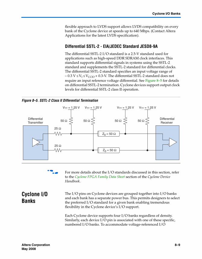
Differential SSTL-2 - EIA/JEDEC Standard JESD8-9A
The differential SSTL-2 I/O standard is a 2.5-V standard used for applications such as high-speed DDR SDRAM clock interfaces. This standard supports differential signals in systems using the SSTL-2 standard and supplements the SSTL-2 standard for differential clocks. The differential SSTL-2 standard specifies an input voltage range of – 0.3 V ≤ VI ≤ VCCIO + 0.3-V. The differential SSTL-2 standard does not require an input reference voltage differential. See Figure 8–5 for details on differential SSTL-2 termination. Cyclone devices support output clock levels for differential SSTL-2 class II operation.
Figure 8–5. SSTL-2 Class II Differential Termination
f For more details about the I/O standards discussed in this section, refer to the Cyclone FPGA Family Data Sheet section of the Cyclone Device Handbook.
Cyclone I/O Banks
The I/O pins on Cyclone devices are grouped together into I/O banks and each bank has a separate power bus. This permits designers to select the preferred I/O standard for a given bank enabling tremendous flexibility in the Cyclone device’s I/O support.
Each Cyclone device supports four I/O banks regardless of density. Similarly, each device I/O pin is associated with one of these specific, numbered I/O banks. To accommodate voltage-referenced I/O
DifferentialTransmitter
DifferentialReceiver
Z0 = 50 Ω
50 Ω 50 Ω
Z0 = 50 Ω
VTT = 1.25 V VTT = 1.25 V
50 Ω 50 Ω
VTT = 1.25 V VTT = 1.25 V
25 Ω
25 Ω
8–10 Altera CorporationPreliminary May 2008
Cyclone Device Handbook, Volume 1
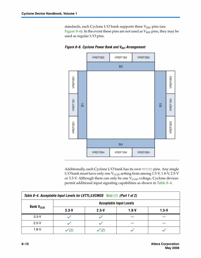
standards, each Cyclone I/O bank supports three VREF pins (see Figure 8–6). In the event these pins are not used as VREF pins, they may be used as regular I/O pins.
Figure 8–6. Cyclone Power Bank and VREF Arrangement
Additionally, each Cyclone I/O bank has its own VCCIO pins. Any single I/O bank must have only one VCCIO setting from among 1.5-V, 1.8-V, 2.5-V or 3.3-V. Although there can only be one VCCIO voltage, Cyclone devices permit additional input signaling capabilities as shown in Table 8–4.
B2
B1
B3
B4
VREF2B2 VREF0B2VREF1B2
VR
EF
2B1
VR
EF
0B1
VR
EF
1B1
VREF2B4 VREF0B4VREF1B4
VR
EF
2B3
VR
EF
0B3
VR
EF
1B3
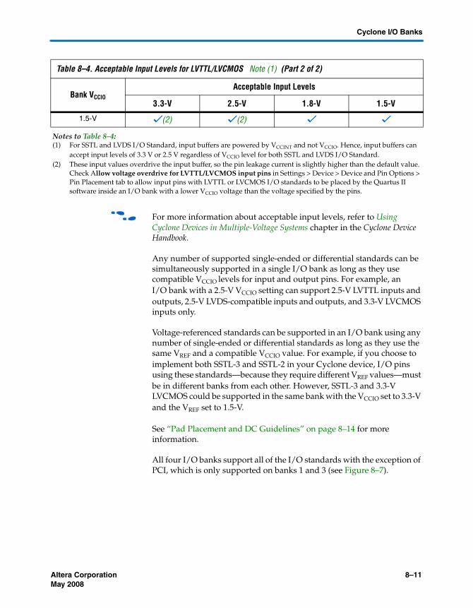
Table 8–4. Acceptable Input Levels for LVTTL/LVCMOS Note (1) (Part 1 of 2)
Bank VCCIO
Acceptable Input Levels
3.3-V 2.5-V 1.8-V 1.5-V
3.3-V v v — —
2.5-V v v — —
1.8-V v(2) v(2) v v
Altera Corporation 8–11May 2008 Preliminary
Cyclone I/O Banks
f For more information about acceptable input levels, refer to Using Cyclone Devices in Multiple-Voltage Systems chapter in the Cyclone Device Handbook.
Any number of supported single-ended or differential standards can be simultaneously supported in a single I/O bank as long as they use compatible VCCIO levels for input and output pins. For example, an I/O bank with a 2.5-V VCCIO setting can support 2.5-V LVTTL inputs and outputs, 2.5-V LVDS-compatible inputs and outputs, and 3.3-V LVCMOS inputs only.
Voltage-referenced standards can be supported in an I/O bank using any number of single-ended or differential standards as long as they use the same VREF and a compatible VCCIO value. For example, if you choose to implement both SSTL-3 and SSTL-2 in your Cyclone device, I/O pins using these standards—because they require different VREF values—must be in different banks from each other. However, SSTL-3 and 3.3-V LVCMOS could be supported in the same bank with the VCCIO set to 3.3-V and the VREF set to 1.5-V.
See “Pad Placement and DC Guidelines” on page 8–14 for more information.
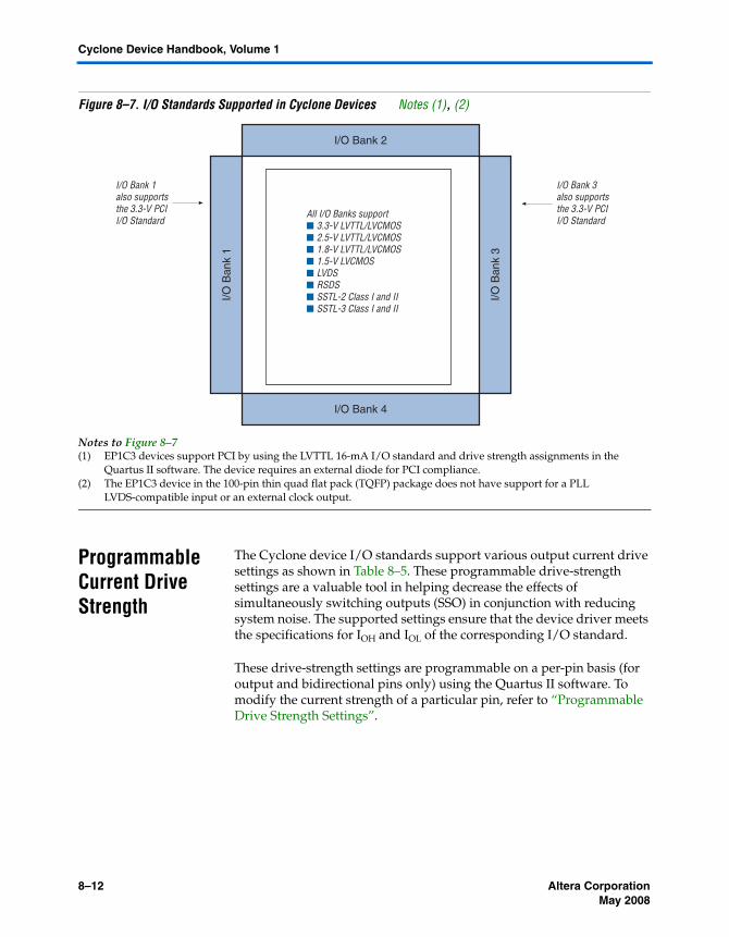
All four I/O banks support all of the I/O standards with the exception of PCI, which is only supported on banks 1 and 3 (see Figure 8–7).
1.5-V v(2) v(2) v v
Notes to Table 8–4:(1) For SSTL and LVDS I/O Standard, input buffers are powered by VCCINT and not VCCIO. Hence, input buffers can
accept input levels of 3.3 V or 2.5 V regardless of VCCIO level for both SSTL and LVDS I/O Standard.(2) These input values overdrive the input buffer, so the pin leakage current is slightly higher than the default value.
Check Allow voltage overdrive for LVTTL/LVCMOS input pins in Settings > Device > Device and Pin Options > Pin Placement tab to allow input pins with LVTTL or LVCMOS I/O standards to be placed by the Quartus II software inside an I/O bank with a lower VCCIO voltage than the voltage specified by the pins.
Table 8–4. Acceptable Input Levels for LVTTL/LVCMOS Note (1) (Part 2 of 2)
Bank VCCIO
Acceptable Input Levels
3.3-V 2.5-V 1.8-V 1.5-V
8–12 Altera CorporationPreliminary May 2008
Cyclone Device Handbook, Volume 1
Figure 8–7. I/O Standards Supported in Cyclone Devices Notes (1), (2)
Notes to Figure 8–7 (1) EP1C3 devices support PCI by using the LVTTL 16-mA I/O standard and drive strength assignments in the
Quartus II software. The device requires an external diode for PCI compliance.(2) The EP1C3 device in the 100-pin thin quad flat pack (TQFP) package does not have support for a PLL
LVDS-compatible input or an external clock output.
Programmable Current Drive Strength
The Cyclone device I/O standards support various output current drive settings as shown in Table 8–5. These programmable drive-strength settings are a valuable tool in helping decrease the effects of simultaneously switching outputs (SSO) in conjunction with reducing system noise. The supported settings ensure that the device driver meets the specifications for IOH and IOL of the corresponding I/O standard.
These drive-strength settings are programmable on a per-pin basis (for output and bidirectional pins only) using the Quartus II software. To modify the current strength of a particular pin, refer to “Programmable Drive Strength Settings”.
I/O Bank 2
I/O B
ank
1
I/O B
ank
3
I/O Bank 4
All I/O Banks support■ 3.3-V LVTTL/LVCMOS■ 2.5-V LVTTL/LVCMOS■ 1.8-V LVTTL/LVCMOS■ 1.5-V LVCMOS■ LVDS■ RSDS■ SSTL-2 Class I and II■ SSTL-3 Class I and II
I/O Bank 1 also supports the 3.3-V PCI I/O Standard
I/O Bank 3 also supports the 3.3-V PCI I/O Standard
Altera Corporation 8–13May 2008 Preliminary
Hot Socketing
Hot Socketing Cyclone devices support any power-up or power-down sequence (VCCIO and VCCINT) to facilitate hot socketing. You can drive signals into the device before or during power-up or power-down without damaging the device. Cyclone devices will not drive out until the device is configured and has attained proper operating conditions.
You can power up or power down the VCCIO and VCCINT pins in any sequence. The power supply ramp rates can range from 100 ns to 100 ms. All VCC supplies must power down within 100 ms of each other to prevent I/O pins from driving out. Additionally, during power-up, the I/O pin capacitance is less than 15 pF and the clock pin capacitance is less than 20pF.
■ The hot socketing DC specification is | IIOPIN | < 300 µA.■ The hot socketing AC specification is | IIOPIN | < 8 mA for 10 ns or
less.
I/O Termination The majority of the Cyclone I/O standards are single-ended, non-voltage-referenced I/O standards and, as such, the following I/O standards do not specify a recommended termination scheme:
■ 3.3-V LVTTL / LVCMOS■ 2.5-V LVTTL / LVCMOS■ 1.8-V LVTTL / LVCMOS■ 1.5-V LVCMOS■ 3.3-V PCI
The Cyclone device family does not feature on-chip I/O termination resistors.
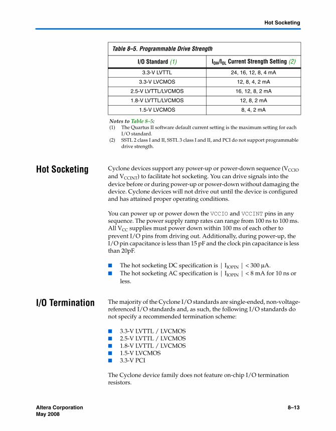
Table 8–5. Programmable Drive Strength
I/O Standard (1) IOH/IOL Current Strength Setting (2)
3.3-V LVTTL 24, 16, 12, 8, 4 mA
3.3-V LVCMOS 12, 8, 4, 2 mA
2.5-V LVTTL/LVCMOS 16, 12, 8, 2 mA
1.8-V LVTTL/LVCMOS 12, 8, 2 mA
1.5-V LVCMOS 8, 4, 2 mA
Notes to Table 8–5:(1) The Quartus II software default current setting is the maximum setting for each
I/O standard.(2) SSTL 2 class I and II, SSTL 3 class I and II, and PCI do not support programmable
drive strength.
8–14 Altera CorporationPreliminary May 2008
Cyclone Device Handbook, Volume 1
Voltage-Referenced I/O Standard Termination
Voltage-referenced I/O standards require both an input reference voltage, VREF, and a termination voltage, VTT. An external pull up to VTT must be provided to the Cyclone device as the device does not have VTT pins. The reference voltage of the receiving device tracks the termination voltage of the transmitting device.
For more information on termination for voltage-referenced I/O standards, refer to “Supported I/O Standards”.
Differential I/O Standard Termination
Differential I/O standards typically require a termination resistor between the two signals at the receiver. The termination resistor must match the differential load impedance of the bus.
LVDS and RSDS are the only differential I/O standards supported by Cyclone devices. For information on LVDS termination and RSDS termination, refer to the LVDS Receiver and Transmitter Termination and RSDS I/O Standard Support in Cyclone Devices sections, respectively, in the High-Speed Differential Signaling in Cyclone Devices chapter in the Cyclone Device Handbook.
Pad Placement and DC Guidelines
This section provides pad placement guidelines for the programmable I/O standards supported by Cyclone devices and includes essential information for designing systems using the devices’ selectable I/O capabilities. This section also discusses the DC limitations and guidelines.
Differential Pad Placement Guidelines
In order to maintain an acceptable noise level on the VCCIO supply, there are restrictions on placement of single-ended I/O pads in relation to differential pads. Use the following guidelines for placing single-ended pads with respect to differential pads in Cyclone devices.
■ Single-ended inputs may be only be placed four or more pads away from a differential pad.
■ Single-ended outputs and bidirectional pads may only be placed five or more pads away from a differential pad.
1 The Quartus II software generates an error message for illegally placed pads.
Altera Corporation 8–15May 2008 Preliminary
Pad Placement and DC Guidelines
VREF Pad Placement Guidelines
In order to maintain an acceptable noise level on the VCCIO supply and to prevent output switching noise from shifting the VREF rail, there are restrictions on the placement of single-ended voltage referenced I/Os with respect to VREF pads and VCCIO/GND pairs. Please use the following guidelines for placing single-ended pads in Cyclone devices.
Input Pads
Each VREF pad supports a maximum of 40 input pads with up to 20 on each side of the VREF pad. This is irrespective of VCCIO/GND pairs.
Output Pads
When a voltage referenced input or bidirectional pad does not exist in a bank, there is no limit to the number of output pads that can be implemented in that bank. When a voltage referenced input exists, each VCCIO/GND pair supports 9 outputs for Fineline BGA® packages or 4 outputs for quad flat pack (QFP) packages. Any output pads must be placed greater than 1 pad away from your VREF pad to maintain acceptable noise levels.
Bidirectional Pads
Bidirectional pads must satisfy input and output guidelines simultaneously. If the bidirectional pads are all controlled by the same OE and there are no other outputs or voltage referenced inputs in the bank, then there is no case where there is a voltage referenced input active at the same time as an output. Therefore, the output limitation does not apply. However, since the bidirectional pads are linked to the same OE, the bidirectional pads will all act as inputs at the same time. Therefore, the input limitation of 40 input pads (20 on each side of your VREF pad) will apply.
8–16 Altera CorporationPreliminary May 2008
Cyclone Device Handbook, Volume 1
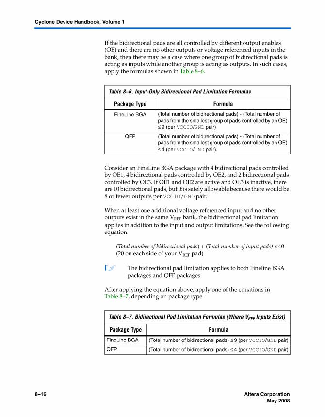
If the bidirectional pads are all controlled by different output enables (OE) and there are no other outputs or voltage referenced inputs in the bank, then there may be a case where one group of bidirectional pads is acting as inputs while another group is acting as outputs. In such cases, apply the formulas shown in Table 8–6.
Consider an FineLine BGA package with 4 bidirectional pads controlled by OE1, 4 bidirectional pads controlled by OE2, and 2 bidirectional pads controlled by OE3. If OE1 and OE2 are active and OE3 is inactive, there are 10 bidirectional pads, but it is safely allowable because there would be 8 or fewer outputs per VCCIO/GND pair.
When at least one additional voltage referenced input and no other outputs exist in the same VREF bank, the bidirectional pad limitation applies in addition to the input and output limitations. See the following equation.
(Total number of bidirectional pads) + (Total number of input pads) ≤ 40 (20 on each side of your VREF pad)
1 The bidirectional pad limitation applies to both Fineline BGA packages and QFP packages.
After applying the equation above, apply one of the equations in Table 8–7, depending on package type.
Table 8–6. Input-Only Bidirectional Pad Limitation Formulas
Package Type Formula
FineLine BGA (Total number of bidirectional pads) - (Total number of pads from the smallest group of pads controlled by an OE) ≤ 9 (per VCCIO/GND pair)
QFP (Total number of bidirectional pads) - (Total number of pads from the smallest group of pads controlled by an OE) ≤ 4 (per VCCIO/GND pair).
Table 8–7. Bidirectional Pad Limitation Formulas (Where VREF Inputs Exist)
Package Type Formula
FineLine BGA (Total number of bidirectional pads) ≤ 9 (per VCCIO/GND pair)
QFP (Total number of bidirectional pads) ≤ 4 (per VCCIO/GND pair)
Altera Corporation 8–17May 2008 Preliminary
Pad Placement and DC Guidelines
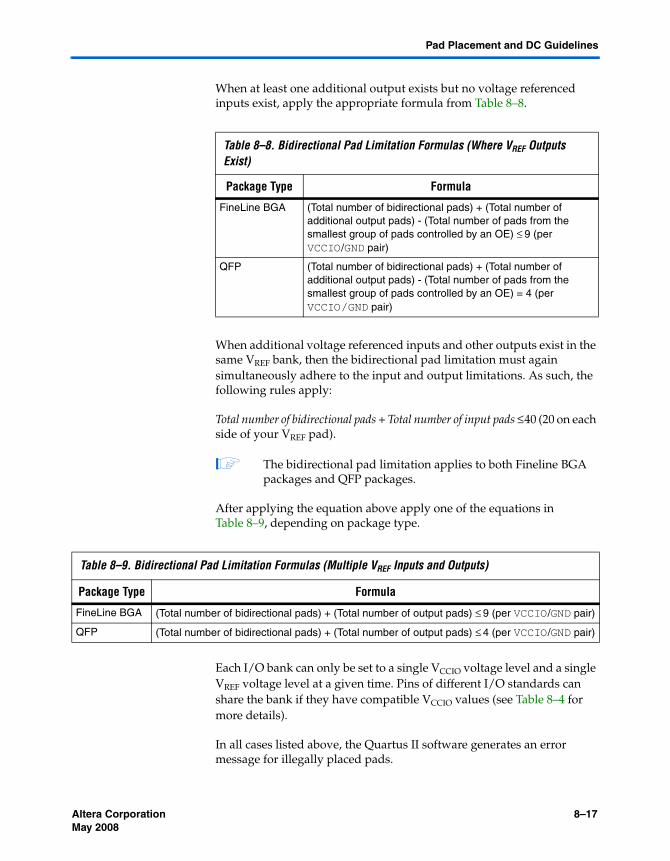
When at least one additional output exists but no voltage referenced inputs exist, apply the appropriate formula from Table 8–8.
When additional voltage referenced inputs and other outputs exist in the same VREF bank, then the bidirectional pad limitation must again simultaneously adhere to the input and output limitations. As such, the following rules apply:
Total number of bidirectional pads + Total number of input pads ≤ 40 (20 on each side of your VREF pad).
1 The bidirectional pad limitation applies to both Fineline BGA packages and QFP packages.
After applying the equation above apply one of the equations in Table 8–9, depending on package type.
Each I/O bank can only be set to a single VCCIO voltage level and a single VREF voltage level at a given time. Pins of different I/O standards can share the bank if they have compatible VCCIO values (see Table 8–4 for more details).
In all cases listed above, the Quartus II software generates an error message for illegally placed pads.
Table 8–8. Bidirectional Pad Limitation Formulas (Where VREF Outputs Exist)
Package Type Formula
FineLine BGA (Total number of bidirectional pads) + (Total number of additional output pads) - (Total number of pads from the smallest group of pads controlled by an OE) ≤ 9 (per VCCIO/GND pair)
QFP (Total number of bidirectional pads) + (Total number of additional output pads) - (Total number of pads from the smallest group of pads controlled by an OE) = 4 (per VCCIO/GND pair)
Table 8–9. Bidirectional Pad Limitation Formulas (Multiple VREF Inputs and Outputs)
Package Type Formula
FineLine BGA (Total number of bidirectional pads) + (Total number of output pads) ≤ 9 (per VCCIO/GND pair)
QFP (Total number of bidirectional pads) + (Total number of output pads) ≤ 4 (per VCCIO/GND pair)
8–18 Altera CorporationPreliminary May 2008
Cyclone Device Handbook, Volume 1
DC Guidelines
There is a current limit of 320 mA per 16 consecutive output pins, as shown by the following equation:
Table 8–10 shows the current allowed per pin by select I/O standards as measured under the standard's defined loading conditions. PCI, LVTTL, LVCMOS, and other supported I/O standards not shown in the table do not have standardized loading conditions. As such, the current allowed per pin in a series-loaded condition for these standards is considered negligible.
Quartus II Software Support
Use the Quartus II software to specify which programmable I/O standards to use for Cyclone devices. This section describes Quartus II implementation, placement, and assignment guidelines, including:
■ Settings■ Device and pin options■ Assigning pins■ Programmable drive strength settings■ I/O banks in the floorplan view■ Auto placement and verification
Settings
The Settings dialog box (Assignments menu) includes options allowing you to set a default I/O standard, optimize for I/O placement, assign I/O pins, and numerous other I/O-related options. The most pertinent user features are described in detail below.
Table 8–10. I/O Standard DC Specification
Pin I/O StandardI Pin (mA)
3.3-V VCCIO 2.5-V VCCIO
SSTL-3 Class I 8 N/A
SSTL-3 Class II 16 N/A
SSTL-2 Class I N/A 8.1
SSTL-2 Class II N/A 16.4
LVDS N/A
Σpin + 15
pin
Ipin < 320 mA
Altera Corporation 8–19May 2008 Preliminary
Quartus II Software Support
Device and Pin Options
To access Device and Pin Options, choose Settings from Assignments menu. From Settings dialog box, click Device and Pin Options. There are numerous categories in the Device and Pin Options dialog box, including General, Configuration, Programming Files, Unused Pins, Dual-Purpose Pins, and Voltage. Similarly, each of these categories contains settings vital to the device operation such as the default I/O standard applied to the device (Voltage tab), how to reserve all unused pins (Unused Pins tab), specify the capacitive load (in picofarads (pF)) on output pins for each I/O standards (Capacitive Loading tab), and whether or not the device should enable a device-wide reset (General tab).
Assigning Pins
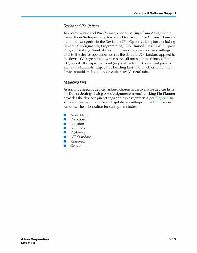
Assuming a specific device has been chosen in the available devices list in the Device Settings dialog box (Assignments menu), clicking Pin Planner provides the device's pin settings and pin assignments (see Figure 8–8). You can view, add, remove and update pin settings in the Pin Planner window. The information for each pin includes:
■ Node Name■ Direction■ Location■ I/O Bank■ Vref Group■ I/O Standard■ Reserved■ Group
8–20 Altera CorporationPreliminary May 2008
Cyclone Device Handbook, Volume 1
Figure 8–8. Assign Pins
1 You can use Filter in the Pin Planner window to list assigned, unassigned, input, output, bidirectional or all pins.
When you assign an I/O standard that requires a reference voltage to an I/O pin, the Quartus II software automatically assigns VREF pins. Refer to Quartus II Help for instructions on how to use an I/O standard for a pin.
Programmable Drive Strength Settings
To specify programmable drive strength settings, perform the following steps:
1. Choose Assignment Editor (Assignments menu).
2. Under To field in the Assignment Editor box, right-click on a new row. Select Node Finder. Click List in the Node Finder window. Then select the output or bidirectional pin for which you will specify the current strength.
3. Set the Assignment Name field to Current Strength (accepts wildcards/groups), then enter the desired value in the Value field.
4. Select Yes under Enabled field to enable the selected current strength.
Altera Corporation 8–21May 2008 Preliminary
Quartus II Software Support
The Quartus II software displays the entire range of drive strength choices. While the Quartus II software does not prohibit you from specifying any of these for your I/O pin, not every setting is supported by every I/O standard. See Table 8–5 for supported combinations.
I/O Banks in the Floorplan View
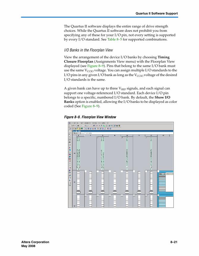
View the arrangement of the device I/O banks by choosing Timing Closure Floorplan (Assignments View menu) with the Floorplan View displayed (see Figure 8–9). Pins that belong to the same I/O bank must use the same VCCIO voltage. You can assign multiple I/O standards to the I/O pins in any given I/O bank as long as the VCCIO voltage of the desired I/O standards is the same.
A given bank can have up to three VREF signals, and each signal can support one voltage-referenced I/O standard. Each device I/O pin belongs to a specific, numbered I/O bank. By default, the Show I/O Banks option is enabled, allowing the I/O banks to be displayed as color coded (See Figure 8–9).
Figure 8–9. Floorplan View Window
8–22 Altera CorporationPreliminary May 2008
Cyclone Device Handbook, Volume 1
Auto Placement and Verification of Selectable I/O Standards
The Quartus II software automatically verifies the placement for all I/O and VREF pins and performs the following actions:
■ Automatically places I/O pins of different VREF standards without pin assignments in separate I/O banks and enables the VREF pins of these I/O banks.
■ Verifies that voltage-referenced I/O pins requiring different VREF levels are not placed in the same bank.
■ Reports an error message if the current limit is exceeded for a Cyclone power bank (See “DC Guidelines”).
■ Automatically assigns VREF pins and I/O pins such that the current requirements are met and I/O standards are placed properly.
Conclusion Cyclone device I/O capabilities enable system designers to keep pace with increasing design complexity utilizing a low-cost FPGA device family. Support for I/O standards including SSTL and LVDS compatibility allow Cyclone devices to fit into a wide variety of applications. The Quartus II software makes it easy to use these I/O standards in Cyclone device designs. After design compilation, the software also provides clear, visual representations of pads and pins and the selected I/O standards. Taking advantage of the support of these I/O standards in Cyclone devices will allow you to lower your design costs without compromising design flexibility or complexity.
More Information
For more information about Cyclone devices refer to the following resources:
■ Cyclone FPGA Family Data Sheet section of the Cyclone Device Handbook
■ Using Cyclone Devices in Multiple-Voltage Systems chapter in the Cyclone Device Handbook
■ AN 75: High-Speed Board Designs
References For more information on the I/O standards referred to in this document, see the following sources:
■ Stub Series Terminated Logic for 2.5-V (SSTL-2), JESD8-9A, Electronic Industries Association, December 2000.
■ 1.5-V +/- 0.1-V (Normal Range) and 0.9-V - 1.6-V (Wide Range) Power Supply Voltage and Interface Standard for Non-terminated Digital Integrated Circuits, JESD8-11, Electronic Industries Association, October 2000.
Altera Corporation 8–23May 2008 Preliminary
Referenced Documents
■ 1.8-V +/- 0.15-V (Normal Range) and 1.2-V - 1.95-V (Wide Range) Power Supply Voltage and Interface Standard for Non-terminated Digital Integrated Circuits, JESD8-7, Electronic Industries Association, February 1997.
■ 2.5-V +/- 0.2-V (Normal Range) and 1.8-V to 2.7-V (Wide Range) Power Supply Voltage and Interface Standard for Non-terminated Digital Integrated Circuits, JESD8-5, Electronic Industries Association, October 1995.
■ Interface Standard for Nominal 3-V/ 3.3-V Supply Digital Integrated Circuits, JESD8-B, Electronic Industries Association, September 1999.
■ PCI Local Bus Specification, Revision 2.2, PCI Special Interest Group, December 1998.
■ Electrical Characteristics of Low Voltage Differential Signaling (LVDS) Interface Circuits, ANSI/TIA/EIA-644, American National Standards Institute/Telecommunications Industry/Electronic Industries Association, October 1995.
Referenced Documents
This chapter references the following documents:
■ AN 75: High-Speed Board Designs■ Cyclone FPGA Family Data Sheet section of the Cyclone Device
Handbook■ High-Speed Differential Signaling in Cyclone Devices chapter in the
Cyclone Device Handbook■ Using Cyclone Devices in Multiple-Voltage Systems chapter in the
Cyclone Device Handbook
Document Revision History
Table 8–11 shows the revision history for this chapter.
Table 8–11. Document Revision History
Date and Document Version Changes Made Summary of
Changes
May 2008v1.6
Minor textual and style changes. Added “Referenced Documents” section.
—
January 2007v1.5
● Added document revision history.● Removed references to “compiler” settings and updated
information in “Quartus II Software Support” section.● Updated Figure 8–8 and the following handpara note.● Updated procedure in “Programmable Drive Strength
Settings” section.● Minor update in “I/O Banks in the Floorplan View”.
—
8–24 Altera CorporationPreliminary May 2008
Cyclone Device Handbook, Volume 1
August 2005v1.4
Minor updates. —
February 2005v1.3
● Updated information concerning hot socketing AC specifications.
● Updated the notes to Figures 8-13 through 8-20.
● Updated text in the Output Pads section. Changed 2 pads away to 1.
—
October 2003v1.2
Updated the 3.3-V (PCI Special Interest Group (SIG) PCI Local Bus Specification Revision 2.2) section.
—
September 2003v1.1
Updated LVDS data rates to 640 Mbps from 311 Mbps. —
May 2003v1.0
Added document to Cyclone Device Handbook. —