Cyclone FPGA Family Data Sheet - Altera · PDF fileDirect link interconnect from adjacent...
97
® Altera Corporation 1 Cyclone FPGA Family April 2003, ver. 1.2 Data Sheet DS-CYCLONE-1.2 Introduction Preliminary Information The Cyclone TM field programmable gate array family is based on a 1.5-V, 0.13-µm, all-layer copper SRAM process, with densities up to 20,060 logic elements (LEs) and up to 288 Kbits of RAM. With features like phase- locked loops (PLLs) for clocking and a dedicated double data rate (DDR) interface to meet DDR SDRAM and fast cycle RAM (FCRAM) memory requirements, Cyclone devices are a cost-effective solution for data-path applications. Cyclone devices support various I/O standards, including LVDS at data rates up to 311 megabits per second (Mbps) and 66-MHz, 32-bit peripheral component interconnect (PCI), for interfacing with and supporting ASSP and ASIC devices. Altera also offers new low-cost serial configuration devices to configure Cyclone devices. Features... ■ 2,910 to 20,060 LEs, see Table 1 ■ Up to 294,912 RAM bits (36,864 bytes) ■ Supports configuration through low-cost serial configuration device ■ Support for LVTTL, LVCMOS, SSTL-2, and SSTL-3 I/O standards ■ Support for 66-MHz, 32-bit PCI standard ■ Low speed (311 Mbps) LVDS I/O support ■ Up to two PLLs per device provide clock multiplication and phase shifting ■ Up to eight global clock lines with six clock resources available per logic array block (LAB) row ■ Support for external memory, including DDR SDRAM (133 MHz), FCRAM, and single data rate (SDR) SDRAM ■ Support for multiple intellectual property (IP) cores, including Altera MegaCore functions and Altera Megafunctions Partners Program (AMPP SM ) megafunctions Note to Table 1: (1) This parameter includes global clock pins. Table 1. Cyclone Device Features Feature EP1C3 EP1C4 EP1C6 EP1C12 EP1C20 LEs 2,910 4,000 5,980 12,060 20,060 M4K RAM blocks (128 × 36 bits) 13 17 20 52 64 Total RAM bits 59,904 78,336 92,160 239,616 294,912 PLLs 1 2 2 2 2 Maximum user I/O pins (1) 104 301 185 249 301
Transcript of Cyclone FPGA Family Data Sheet - Altera · PDF fileDirect link interconnect from adjacent...

®
CycloneFPGA Family
April 2003, ver. 1.2 Data Sheet
Altera Corporation 1
Introduction
Preliminary Information
The CycloneTM field programmable gate array family is based on a 1.5-V, 0.13-µm, all-layer copper SRAM process, with densities up to 20,060 logic elements (LEs) and up to 288 Kbits of RAM. With features like phase-locked loops (PLLs) for clocking and a dedicated double data rate (DDR) interface to meet DDR SDRAM and fast cycle RAM (FCRAM) memory requirements, Cyclone devices are a cost-effective solution for data-path applications. Cyclone devices support various I/O standards, including LVDS at data rates up to 311 megabits per second (Mbps) and 66-MHz, 32-bit peripheral component interconnect (PCI), for interfacing with and supporting ASSP and ASIC devices. Altera also offers new low-cost serial configuration devices to configure Cyclone devices.
Features... 2,910 to 20,060 LEs, see Table 1 Up to 294,912 RAM bits (36,864 bytes) Supports configuration through low-cost serial configuration device Support for LVTTL, LVCMOS, SSTL-2, and SSTL-3 I/O standards Support for 66-MHz, 32-bit PCI standard Low speed (311 Mbps) LVDS I/O support Up to two PLLs per device provide clock multiplication and phase
shifting Up to eight global clock lines with six clock resources available per
logic array block (LAB) row Support for external memory, including DDR SDRAM (133 MHz),
FCRAM, and single data rate (SDR) SDRAM Support for multiple intellectual property (IP) cores, including
Altera MegaCore functions and Altera Megafunctions Partners Program (AMPPSM) megafunctions
Note to Table 1:(1) This parameter includes global clock pins.
Table 1. Cyclone Device Features
Feature EP1C3 EP1C4 EP1C6 EP1C12 EP1C20
LEs 2,910 4,000 5,980 12,060 20,060
M4K RAM blocks (128 × 36 bits) 13 17 20 52 64
Total RAM bits 59,904 78,336 92,160 239,616 294,912
PLLs 1 2 2 2 2
Maximum user I/O pins (1) 104 301 185 249 301
DS-CYCLONE-1.2

Cyclone FPGA Family Data Sheet Preliminary Information
Cyclone devices are available in quad flat pack (QFP) and space-saving FineLine BGA packages (see Tables 2 through 3).
Notes to Table 2:(1) TQFP: thin quad flat pack.
PQFP: plastic quad flat pack.(2) Cyclone devices support vertical migration within the same package (i.e., designers can migrate between the EP1C3
device in the 144-pin TQFP package and the EP1C6 device in the same package).
Table 2. Cyclone Package Options & I/O Pin Counts
Device 100-Pin TQFP (1)
144-Pin TQFP (1), (2)
240-Pin PQFP (1)
256-Pin FineLine
BGA
324-Pin FineLine
BGA
400-Pin FineLine
BGA
EP1C3 65 104
EP1C4 249 301
EP1C6 98 185 185
EP1C12 173 185 249
EP1C20 233 301
Table 3. Cyclone QFP & FineLine BGA Package Sizes
Dimension 100-Pin TQFP
144-Pin TQFP
240-Pin PQFP
256-Pin FineLine
BGA
324-Pin FineLine
BGA
400-Pin FineLine
BGA
Pitch (mm) 0.5 0.5 0.5 1.0 1.0 1.0
Area (mm2) 256 484 1,024 289 361 441
Length × width (mm × mm)
16 × 16 22 × 22 34.6 × 34.6 17 × 17 19 × 19 21 × 21
2 Altera Corporation

Preliminary Information Cyclone FPGA Family Data Sheet
Table of Contents
Introduction ........................................................................................................1Features ...............................................................................................................1Table of Contents ...............................................................................................3Functional Description......................................................................................4Logic Array Blocks.............................................................................................6Logic Elements ...................................................................................................9MultiTrack Interconnect .................................................................................17Embedded Memory.........................................................................................23Global Clock Network & Phase-Locked Loops...........................................34I/O Structure ....................................................................................................44Power Sequencing & Hot Socketing .............................................................60IEEE Std. 1149.1 (JTAG) Boundary Scan Support .......................................60SignalTap II Embedded Logic Analyzer ......................................................65Configuration ...................................................................................................65Operating Conditions......................................................................................67Power Consumption........................................................................................73Timing Model ...................................................................................................74Software.............................................................................................................94Device Pin-Outs ...............................................................................................94Ordering Information......................................................................................94
Altera Corporation 3
Cyclone FPGA Family Data Sheet Preliminary Information
Functional Description
Cyclone devices contain a two-dimensional row- and column-based architecture to implement custom logic. Column and row interconnects of varying speeds provide signal interconnects between LABs and embedded memory blocks.
The logic array consists of LABs, with 10 LEs in each LAB. An LE is a small unit of logic providing efficient implementation of user logic functions. LABs are grouped into rows and columns across the device. Cyclone devices range between 2,910 to 20,060 LEs.
M4K RAM blocks are true dual-port memory blocks with 4K bits of memory plus parity (4,608 bits). These blocks provide dedicated true dual-port, simple dual-port, or single-port memory up to 36-bits wide at up to 200 MHz. These blocks are grouped into columns across the device in between certain LABs. Cyclone devices offer between 60 to 288 Kbits of embedded RAM.
Each Cyclone device I/O pin is fed by an I/O element (IOE) located at the ends of LAB rows and columns around the periphery of the device. I/O pins support various single-ended and differential I/O standards, such as the 66-MHz, 32-bit PCI standard and the LVDS I/O standard at up to 311 Mbps. Each IOE contains a bidirectional I/O buffer and three registers for registering input, output, and output-enable signals. Dual-purpose DQS, DQ, and DM pins along with delay chains (used to phase-align DDR signals) provide interface support with external memory devices such as DDR SDRAM, and FCRAM devices at up to 133 MHz (266 Mbps).
Cyclone devices provide a global clock network and up to two PLLs. The global clock network consists of eight global clock lines that drive throughout the entire device. The global clock network can provide clocks for all resources within the device, such as IOEs, LEs, and memory blocks. The global clock lines can also be used for control signals. Cyclone PLLs provide general-purpose clocking with clock multiplication and phase shifting as well as external outputs for high-speed differential I/O support.
Figure 1 shows a diagram of the Cyclone EP1C12 device.
4 Altera Corporation

Preliminary Information Cyclone FPGA Family Data Sheet
Figure 1. Cyclone EP1C12 Device Block Diagram
The number of M4K RAM blocks, PLLs, rows, and columns vary per device. Table 4 lists the resources available in each Cyclone device.
Logic Array
PLL
IOEs
M4K Blocks
EP1C12 Device
Table 4. Cyclone Device Resources
Device M4K RAM PLLs LAB Columns LAB Rows
Columns Blocks
EP1C3 1 13 1 24 13
EP1C4 1 17 2 26 17
EP1C6 1 20 2 32 20
EP1C12 2 52 2 48 26
EP1C20 2 64 2 64 32
Altera Corporation 5

Cyclone FPGA Family Data Sheet Preliminary Information
Logic Array Blocks
Each LAB consists of 10 LEs, LE carry chains, LAB control signals, a local interconnect, look-up table (LUT) chain, and register chain connection lines. The local interconnect transfers signals between LEs in the same LAB. LUT chain connections transfer the output of one LE’s LUT to the adjacent LE for fast sequential LUT connections within the same LAB. Register chain connections transfer the output of one LE’s register to the adjacent LE’s register within an LAB. The Quartus® II Compiler places associated logic within an LAB or adjacent LABs, allowing the use of local, LUT chain, and register chain connections for performance and area efficiency. Figure 2 details the Cyclone LAB.
Figure 2. Cyclone LAB Structure
Direct linkinterconnect fromadjacent block
Direct linkinterconnect toadjacent block
Row Interconnect
Column Interconnect
Local InterconnectLAB
Direct linkinterconnect from adjacent block
Direct linkinterconnect toadjacent block
6 Altera Corporation

Preliminary Information Cyclone FPGA Family Data Sheet
LAB Interconnects
The LAB local interconnect can drive LEs within the same LAB. The LAB local interconnect is driven by column and row interconnects and LE outputs within the same LAB. Neighboring LABs, PLLs, and M4K RAM blocks from the left and right can also drive an LAB’s local interconnect through the direct link connection. The direct link connection feature minimizes the use of row and column interconnects, providing higher performance and flexibility. Each LE can drive 30 other LEs through fast local and direct link interconnects. Figure 3 shows the direct link connection.
Figure 3. Direct Link Connection
LAB Control Signals
Each LAB contains dedicated logic for driving control signals to its LEs. The control signals include two clocks, two clock enables, two asynchronous clears, synchronous clear, asynchronous preset/load, synchronous load, and add/subtract control signals. This gives a maximum of 10 control signals at a time. Although synchronous load and clear signals are generally used when implementing counters, they can also be used with other functions.
LAB
Direct linkinterconnectto right
Direct link interconnect fromright LAB, M4K memoryblock, PLL, or IOE output
Direct link interconnect fromleft LAB, M4K memory
block, PLL, or IOE output
LocalInterconnect
Direct linkinterconnect
to left
Altera Corporation 7
Cyclone FPGA Family Data Sheet Preliminary Information
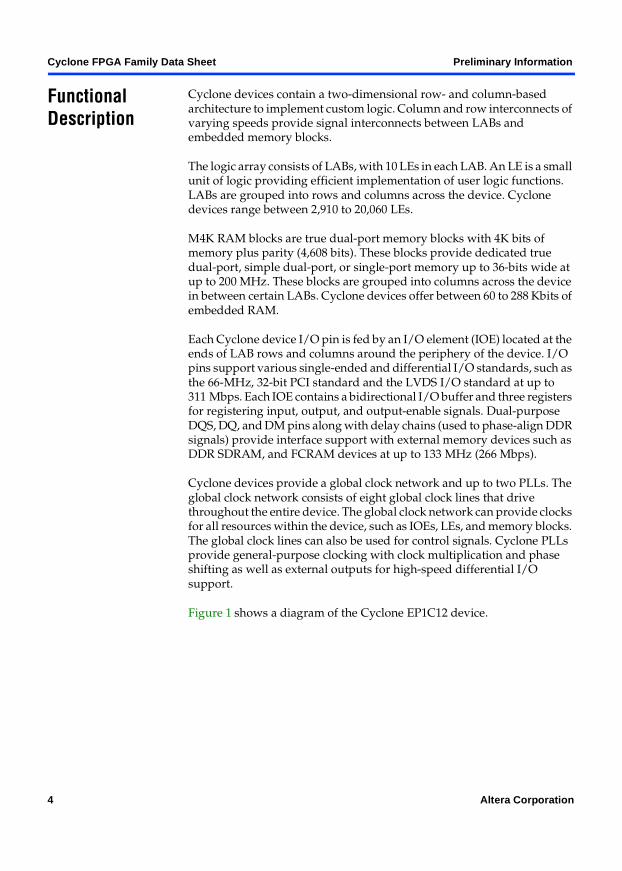
Each LAB can use two clocks and two clock enable signals. Each LAB’s clock and clock enable signals are linked. For example, any LE in a particular LAB using the labclk1 signal will also use labclkena1. If the LAB uses both the rising and falling edges of a clock, it also uses both LAB-wide clock signals. De-asserting the clock enable signal will turn off the LAB-wide clock.
Each LAB can use two asynchronous clear signals and an asynchronous load/preset signal. The asynchronous load acts as a preset when the asynchronous load data input is tied high.
With the LAB-wide addnsub control signal, a single LE can implement a one-bit adder and subtractor. This saves LE resources and improves performance for logic functions such as DSP correlators and signed multipliers that alternate between addition and subtraction depending on data.
The LAB row clocks [5..0] and LAB local interconnect generate the LAB-wide control signals. The MultiTrackTM interconnect’s inherent low skew allows clock and control signal distribution in addition to data. Figure 4 shows the LAB control signal generation circuit.
Figure 4. LAB-Wide Control Signals
labclkena1
labclk2labclk1
labclkena2
asyncloador labpre
syncload
DedicatedLAB RowClocks
LocalInterconnect
LocalInterconnect
LocalInterconnect
LocalInterconnect
LocalInterconnect
LocalInterconnect
labclr1
labclr2
synclr
addnsub
6
8 Altera Corporation
Preliminary Information Cyclone FPGA Family Data Sheet
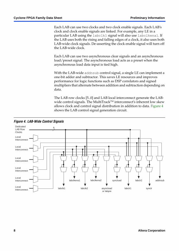
Logic Elements The smallest unit of logic in the Cyclone architecture, the LE, is compact and provides advanced features with efficient logic utilization. Each LE contains a four-input LUT, which is a function generator that can implement any function of four variables. In addition, each LE contains a programmable register and carry chain with carry select capability. A single LE also supports dynamic single bit addition or subtraction mode selectable by an LAB-wide control signal. Each LE drives all types of interconnects: local, row, column, LUT chain, register chain, and direct link interconnects. See Figure 5.
Figure 5. Cyclone LE
labclk1
labclk2
labclr2labpre/aload
Carry-In1
Carry-In0
LAB Carry-In
Clock &Clock Enable
Select
LAB Carry-Out
Carry-Out1
Carry-Out0
Look-UpTable(LUT)
CarryChain
Row, column,and direct link routing
Row, column,and direct link routing
ProgrammableRegister
PRN/ALD
CLRN
D Q
ENA
Register Bypass
PackedRegister Select
Chip-WideReset
labclkena1labclkena2
SynchronousLoad andClear Logic
LAB-wideSynchronous
LoadLAB-wide
SynchronousClear
AsynchronousClear/Preset/Load Logic
data1
data2data3
data4
LUT chainrouting to next LE
labclr1
Local Routing
Register chainoutput
ADATA
addnsub
RegisterFeedback
Register chainrouting fromprevious LE
Altera Corporation 9

Cyclone FPGA Family Data Sheet Preliminary Information
Each LE’s programmable register can be configured for D, T, JK, or SR operation. Each register has data, true asynchronous load data, clock, clock enable, clear, and asynchronous load/preset inputs. Global signals, general-purpose I/O pins, or any internal logic can drive the register’s clock and clear control signals. Either general-purpose I/O pins or internal logic can drive the clock enable, preset, asynchronous load, and asynchronous data. The asynchronous load data input comes from the data3 input of the LE. For combinatorial functions, the LUT output bypasses the register and drives directly to the LE outputs.
Each LE has three outputs that drive the local, row, and column routing resources. The LUT or register output can drive these three outputs independently. Two LE outputs drive column or row and direct link routing connections and one drives local interconnect resources. This allows the LUT to drive one output while the register drives another output. This feature, called register packing, improves device utilization because the device can use the register and the LUT for unrelated functions. Another special packing mode allows the register output to feed back into the LUT of the same LE so that the register is packed with its own fan-out LUT. This provides another mechanism for improved fitting. The LE can also drive out registered and unregistered versions of the LUT output.
LUT Chain & Register Chain
In addition to the three general routing outputs, the LEs within an LAB have LUT chain and register chain outputs. LUT chain connections allow LUTs within the same LAB to cascade together for wide input functions. Register chain outputs allow registers within the same LAB to cascade together. The register chain output allows an LAB to use LUTs for a single combinatorial function and the registers to be used for an unrelated shift register implementation. These resources speed up connections between LABs while saving local interconnect resources. See “MultiTrack Interconnect” on page 17 for more information on LUT chain and register chain connections.
10 Altera Corporation
Preliminary Information Cyclone FPGA Family Data Sheet
addnsub Signal
The LE’s dynamic adder/subtractor feature saves logic resources by using one set of LEs to implement both an adder and a subtractor. This feature is controlled by the LAB-wide control signal addnsub. The addnsub signal sets the LAB to perform either A + B or A − B. The LUT computes addition; subtraction is computed by adding the two’s complement of the intended subtractor. The LAB-wide signal converts to two’s complement by inverting the B bits within the LAB and setting carry-in = 1 to add one to the least significant bit (LSB). The LSB of an adder/subtractor must be placed in the first LE of the LAB, where the LAB-wide addnsub signal automatically sets the carry-in to 1. The Quartus II Compiler automatically places and uses the adder/subtractor feature when using adder/subtractor parameterized functions.
LE Operating Modes
The Cyclone LE can operate in one of the following modes:
Normal mode Dynamic arithmetic mode
Each mode uses LE resources differently. In each mode, eight available inputs to the LE the four data inputs from the LAB local interconnect, carry-in0 and carry-in1 from the previous LE, the LAB carry-in from the previous carry-chain LAB, and the register chain connection are directed to different destinations to implement the desired logic function. LAB-wide signals provide clock, asynchronous clear, asynchronous preset/load, synchronous clear, synchronous load, and clock enable control for the register. These LAB-wide signals are available in all LE modes. The addnsub control signal is allowed in arithmetic mode.
The Quartus II software, in conjunction with parameterized functions such as library of parameterized modules (LPM) functions, automatically chooses the appropriate mode for common functions such as counters, adders, subtractors, and arithmetic functions. If required, the designer can also create special-purpose functions that specify which LE operating mode to use for optimal performance.
Altera Corporation 11

Cyclone FPGA Family Data Sheet Preliminary Information
Normal Mode
The normal mode is suitable for general logic applications and combinatorial functions. In normal mode, four data inputs from the LAB local interconnect are inputs to a four-input LUT (see Figure 6). The Quartus II Compiler automatically selects the carry-in or the data3 signal as one of the inputs to the LUT. Each LE can use LUT chain connections to drive its combinatorial output directly to the next LE in the LAB. Asynchronous load data for the register comes from the data3 input of the LE. LEs in normal mode support packed registers.
Figure 6. LE in Normal Mode
Note to Figure 6:(1) This signal is only allowed in normal mode if the LE is at the end of an adder/subtractor chain.
data1
4-InputLUT
data2
data3cin (from coutof previous LE)
data4
addnsub (LAB Wide)
clock (LAB Wide)
ena (LAB Wide)
aclr (LAB Wide)
aload(LAB Wide)
ALD/PRE
CLRN
DQ
ENA
ADATA
sclear(LAB Wide)
sload(LAB Wide)
Register chainconnection
LUT chainconnection
Registerchain output
Row, column, anddirect link routing
Row, column, anddirect link routing
Local routing
Register Feedback
(1)
12 Altera Corporation

Preliminary Information Cyclone FPGA Family Data Sheet
Dynamic Arithmetic Mode
The dynamic arithmetic mode is ideal for implementing adders, counters, accumulators, wide parity functions, and comparators. An LE in dynamic arithmetic mode uses four 2-input LUTs configurable as a dynamic adder/subtractor. The first two 2-input LUTs compute two summations based on a possible carry-in of 1 or 0; the other two LUTs generate carry outputs for the two chains of the carry select circuitry. As shown in Figure 7, the LAB carry-in signal selects either the carry-in0 or carry-in1 chain. The selected chain’s logic level in turn determines which parallel sum is generated as a combinatorial or registered output. For example, when implementing an adder, the sum output is the selection of two possible calculated sums:
data1 + data2 + carry-in0 or data1 + data2 + carry-in1.
The other two LUTs use the data1 and data2 signals to generate two possible carry-out signals one for a carry of 1 and the other for a carry of 0. The carry-in0 signal acts as the carry select for the carry-out0 output and carry-in1 acts as the carry select for the carry-out1 output. LEs in arithmetic mode can drive out registered and unregistered versions of the LUT output.
The dynamic arithmetic mode also offers clock enable, counter enable, synchronous up/down control, synchronous clear, synchronous load, and dynamic adder/subtractor options. The LAB local interconnect data inputs generate the counter enable and synchronous up/down control signals. The synchronous clear and synchronous load options are LAB-wide signals that affect all registers in the LAB. The Quartus II software automatically places any registers that are not used by the counter into other LABs. The addnsub LAB-wide signal controls whether the LE acts as an adder or subtractor.
Altera Corporation 13

Cyclone FPGA Family Data Sheet Preliminary Information
Figure 7. LE in Dynamic Arithmetic Mode
Note to Figure 7:(1) The addnsub signal is tied to the carry input for the first LE of a carry chain only.
Carry-Select Chain
The carry-select chain provides a very fast carry-select function between LEs in dynamic arithmetic mode. The carry-select chain uses the redundant carry calculation to increase the speed of carry functions. The LE is configured to calculate outputs for a possible carry-in of 0 and carry-in of 1 in parallel. The carry-in0 and carry-in1 signals from a lower-order bit feed forward into the higher-order bit via the parallel carry chain and feed into both the LUT and the next portion of the carry chain. Carry-select chains can begin in any LE within an LAB.
The speed advantage of the carry-select chain is in the parallel pre-computation of carry chains. Since the LAB carry-in selects the precomputed carry chain, not every LE is in the critical path. Only the propagation delays between LAB carry-in generation (LE 5 and LE 10) are now part of the critical path. This feature allows the Cyclone architecture to implement high-speed counters, adders, multipliers, parity functions, and comparators of arbitrary width.
data1 LUTdata2data3
addnsub(LAB Wide)
clock (LAB Wide)
ena (LAB Wide)
aclr (LAB Wide)
ALD/PRE
CLRN
DQ
ENA
ADATA
Register chainconnection
LUT
LUT
LUT
Carry-Out1Carry-Out0
LAB Carry-In
Carry-In0Carry-In1
(1)
sclear(LAB Wide)
sload(LAB Wide)
LUT chainconnection
Registerchain output
Row, column, anddirect link routing
Row, column, anddirect link routing
Local routing
aload(LAB Wide)
Register Feedback
14 Altera Corporation

Preliminary Information Cyclone FPGA Family Data Sheet
Figure 8 shows the carry-select circuitry in an LAB for a 10-bit full adder. One portion of the LUT generates the sum of two bits using the input signals and the appropriate carry-in bit; the sum is routed to the output of the LE. The register can be bypassed for simple adders or used for accumulator functions. Another portion of the LUT generates carry-out bits. An LAB-wide carry-in bit selects which chain is used for the addition of given inputs. The carry-in signal for each chain, carry-in0 or carry-in1, selects the carry-out to carry forward to the carry-in signal of the next-higher-order bit. The final carry-out signal is routed to an LE, where it is fed to local, row, or column interconnects.
Altera Corporation 15

Cyclone FPGA Family Data Sheet Preliminary Information
Figure 8. Carry Select Chain
The Quartus II Compiler automatically creates carry chain logic during design processing, or the designer can create it manually during design entry. Parameterized functions such as LPM functions automatically take advantage of carry chains for the appropriate functions.
The Quartus II Compiler creates carry chains longer than 10 LEs by linking LABs together automatically. For enhanced fitting, a long carry chain runs vertically allowing fast horizontal connections to M4K memory blocks. A carry chain can continue as far as a full column.
LE4
LE3
LE2
LE1A1B1
A2B2
A3B3
A4B4
Sum1
Sum2
Sum3
Sum4
LE10
LE9
LE8
LE7A7B7
A8B8
A9B9
A10B10
Sum7
LE6A6B6
Sum6
LE5A5B5
Sum5
Sum8
Sum9
Sum10
0 1
0 1LAB Carry-In
LAB Carry-Out
LUT
LUT
LUT
LUT
data1
LAB Carry-In
data2
Carry-In0
Carry-In1
Carry-Out0 Carry-Out1
Sum
16 Altera Corporation

Preliminary Information Cyclone FPGA Family Data Sheet
Clear & Preset Logic Control
LAB-wide signals control the logic for the register’s clear and preset signals. The LE directly supports an asynchronous clear and preset function. The register preset is achieved through the asynchronous load of a logic high. The direct asynchronous preset does not require a NOT-gate push-back technique. Cyclone devices support simultaneous preset/ asynchronous load and clear signals. An asynchronous clear signal takes precedence if both signals are asserted simultaneously. Each LAB supports up to two clears and one preset signal.
In addition to the clear and preset ports, Cyclone devices provide a chip-wide reset pin (DEV_CLRn) that resets all registers in the device. An option set before compilation in the Quartus II software controls this pin. This chip-wide reset overrides all other control signals.
MultiTrack Interconnect
In the Cyclone architecture, connections between LEs, M4K memory blocks, and device I/O pins are provided by the MultiTrack interconnect structure with DirectDriveTM technology. The MultiTrack interconnect consists of continuous, performance-optimized routing lines of different speeds used for inter- and intra-design block connectivity. The Quartus II Compiler automatically places critical design paths on faster interconnects to improve design performance.
DirectDrive technology is a deterministic routing technology that ensures identical routing resource usage for any function regardless of placement within the device. The MultiTrack interconnect and DirectDrive technology simplify the integration stage of block-based designing by eliminating the re-optimization cycles that typically follow design changes and additions.
The MultiTrack interconnect consists of row and column interconnects that span fixed distances. A routing structure with fixed length resources for all devices allows predictable and repeatable performance when migrating through different device densities. Dedicated row interconnects route signals to and from LABs, PLLs, and M4K memory blocks within the same row. These row resources include:
Direct link interconnects between LABs and adjacent blocks R4 interconnects traversing four blocks to the right or left
The direct link interconnect allows an LAB or M4K memory block to drive into the local interconnect of its left and right neighbors. Only one side of a PLL block interfaces with direct link and row interconnects. The direct link interconnect provides fast communication between adjacent LABs and/or blocks without using row interconnect resources.
Altera Corporation 17

Cyclone FPGA Family Data Sheet Preliminary Information
The R4 interconnects span four LABs, or two LABs and one M4K RAM block. These resources are used for fast row connections in a four-LAB region. Every LAB has its own set of R4 interconnects to drive either left or right. Figure 9 shows R4 interconnect connections from an LAB. R4 interconnects can drive and be driven by M4K memory blocks, PLLs, and row IOEs. For LAB interfacing, a primary LAB or LAB neighbor can drive a given R4 interconnect. For R4 interconnects that drive to the right, the primary LAB and right neighbor can drive on to the interconnect. For R4 interconnects that drive to the left, the primary LAB and its left neighbor can drive on to the interconnect. R4 interconnects can drive other R4 interconnects to extend the range of LABs they can drive. R4 interconnects can also drive C4 interconnects for connections from one row to another.
Figure 9. R4 Interconnect Connections
Notes to Figure 9:(1) C4 interconnects can drive R4 interconnects.(2) This pattern is repeated for every LAB in the LAB row.
The column interconnect operates similarly to the row interconnect. Each column of LABs is served by a dedicated column interconnect, which vertically routes signals to and from LABs, M4K memory blocks, and row and column IOEs. These column resources include:
LUT chain interconnects within an LAB Register chain interconnects within an LAB C4 interconnects traversing a distance of four blocks in an up and
down direction
PrimaryLAB (2)
R4 InterconnectDriving Left
Adjacent LAB canDrive onto AnotherLAB's R4 Interconnect
C4 Column Interconnects (1)R4 InterconnectDriving Right
LABNeighbor
LABNeighbor
18 Altera Corporation

Preliminary Information Cyclone FPGA Family Data Sheet
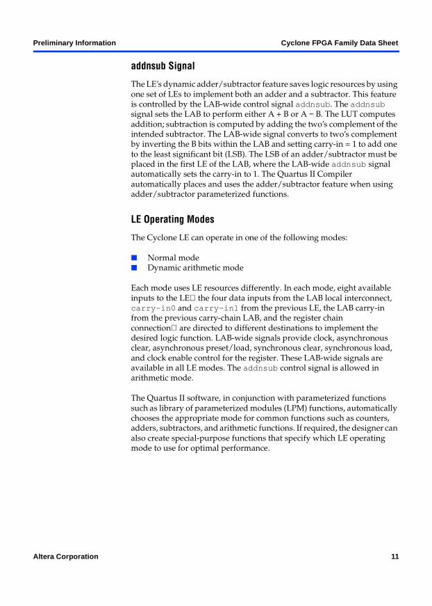
Cyclone devices include an enhanced interconnect structure within LABs for routing LE output to LE input connections faster using LUT chain connections and register chain connections. The LUT chain connection allows the combinatorial output of an LE to directly drive the fast input of the LE right below it, bypassing the local interconnect. These resources can be used as a high-speed connection for wide fan-in functions from LE 1 to LE 10 in the same LAB. The register chain connection allows the register output of one LE to connect directly to the register input of the next LE in the LAB for fast shift registers. The Quartus II Compiler automatically takes advantage of these resources to improve utilization and performance. Figure 10 shows the LUT chain and register chain interconnects.
Altera Corporation 19
Cyclone FPGA Family Data Sheet Preliminary Information
Figure 10. LUT Chain & Register Chain Interconnects
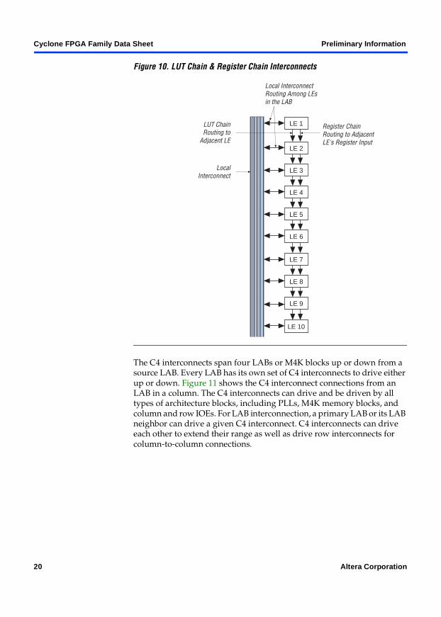
The C4 interconnects span four LABs or M4K blocks up or down from a source LAB. Every LAB has its own set of C4 interconnects to drive either up or down. Figure 11 shows the C4 interconnect connections from an LAB in a column. The C4 interconnects can drive and be driven by all types of architecture blocks, including PLLs, M4K memory blocks, and column and row IOEs. For LAB interconnection, a primary LAB or its LAB neighbor can drive a given C4 interconnect. C4 interconnects can drive each other to extend their range as well as drive row interconnects for column-to-column connections.
LE 1
LE 2
LE 3
LE 4
LE 5
LE 6
LE 7
LE 8
LE 9
LE 10
LUT ChainRouting to
Adjacent LE
LocalInterconnect
Register ChainRouting to AdjacentLE's Register Input
Local InterconnectRouting Among LEsin the LAB
20 Altera Corporation

Preliminary Information Cyclone FPGA Family Data Sheet
Figure 11. C4 Interconnect Connections Note (1)
Note to Figure 11:(1) Each C4 interconnect can drive either up or down four rows.
C4 InterconnectDrives Local and R4InterconnectsUp to Four Rows
Adjacent LAB candrive onto neighboringLAB's C4 interconnect
C4 InterconnectDriving Up
C4 InterconnectDriving Down
LAB
RowInterconnect
LocalInterconnect
Altera Corporation 21

Cyclone FPGA Family Data Sheet Preliminary Information
All embedded blocks communicate with the logic array similar to LAB-to-LAB interfaces. Each block (i.e., M4K memory or PLL) connects to row and column interconnects and has local interconnect regions driven by row and column interconnects. These blocks also have direct link interconnects for fast connections to and from a neighboring LAB.
Table 5 shows the Cyclone device’s routing scheme.
Table 5. Cyclone Device Routing Scheme
Source Destination
LUT
Chai
n
Regi
ster
Cha
in
Loca
l Int
erco
nnec
t
Dire
ct L
ink
Inte
rcon
nect
R4 In
terc
onne
ct
C4 In
terc
onne
ct
LE M4K
RAM
Blo
ck
PLL
Colu
mn
IOE
Row
IOE
LUT Chain v
Register Chain v
Local Interconnect v v v v v
Direct Link Interconnect
v
R4 Interconnect v v v
C4 Interconnect v v v
LE v v v v v v
M4K RAM Block v v v v
PLL v v v
Column IOE v
Row IOE v v v
22 Altera Corporation

Preliminary Information Cyclone FPGA Family Data Sheet
Embedded Memory
The Cyclone embedded memory consists of columns of M4K memory blocks. EP1C3 and EP1C6 devices have one column of M4K blocks, while EP1C12 and EP1C20 devices have two columns (see Table 1 on page 1 for total RAM bits per density). Each M4K block can implement various types of memory with or without parity, including true dual-port, simple dual-port, and single-port RAM, ROM, and FIFO buffers. The M4K blocks support the following features:
4,608 RAM bits 200 MHz performance True dual-port memory Simple dual-port memory Single-port memory Byte enable Parity bits Shift register FIFO buffer ROM Mixed clock mode
Memory Modes
The M4K memory blocks include input registers that synchronize writes and output registers to pipeline designs and improve system performance. M4K blocks offer a true dual-port mode to support any combination of two-port operations: two reads, two writes, or one read and one write at two different clock frequencies. Figure 12 shows true dual-port memory.
Figure 12. True Dual-Port Memory Configuration
In addition to true dual-port memory, the M4K memory blocks support simple dual-port and single-port RAM. Simple dual-port memory supports a simultaneous read and write. Single-port memory supports non-simultaneous reads and writes. Figure 13 shows these different M4K RAM memory port configurations.
dataA[ ]addressA[ ]wrenA
clockA
clockenA
qA[ ]aclrA
dataB[ ]addressB[ ]
wrenB
clockB clockenB
qB[ ]aclrB
A B
Altera Corporation 23

Cyclone FPGA Family Data Sheet Preliminary Information
Figure 13. Simple Dual-Port & Single-Port Memory Configurations
Note to Figure 13:(1) Two single-port memory blocks can be implemented in a single M4K block as long
as each of the two independent block sizes is equal to or less than half of the M4K block size.
The memory blocks also enable mixed-width data ports for reading and writing to the RAM ports in dual-port RAM configuration. For example, the memory block can be written in ×1 mode at port A and read out in ×16 mode from port B.
The Cyclone memory architecture can implement fully synchronous RAM by registering both the input and output signals to the M4K RAM block. All M4K memory block inputs are registered, providing synchronous write cycles. In synchronous operation, the memory block generates its own self-timed strobe write enable (wren) signal derived from a global clock. In contrast, a circuit using asynchronous RAM must generate the RAM wren signal while ensuring its data and address signals meet setup and hold time specifications relative to the wren signal. The output registers can be bypassed. Pseudo-asynchronous reading is possible in the simple dual-port mode of M4K blocks by clocking the read enable and read address registers on the negative clock edge and bypassing the output registers.
data[ ]wraddress[ ]wren inclockinclockeninaclr
rdaddress[ ]rden
q[ ]outclock outclocken
outaclr
data[ ]address[ ]wren inclockinclockeninaclr
q[ ]outclock outclocken
outaclr
Single-Port Memory (1)
Simple Dual-Port Memory
24 Altera Corporation

Preliminary Information Cyclone FPGA Family Data Sheet
When configured as RAM or ROM, the designer can use an initialization file to pre-load the memory contents.
Two single-port memory blocks can be implemented in a single M4K block as long as each of the two independent block sizes is equal to or less than half of the M4K block size.
The Quartus II software automatically implements larger memory by combining multiple M4K memory blocks. For example, two 256 × 16-bit RAM blocks can be combined to form a 256 × 32-bit RAM block. Memory performance does not degrade for memory blocks using the maximum number of words allowed. Logical memory blocks using less than the maximum number of words use physical blocks in parallel, eliminating any external control logic that would increase delays. To create a larger high-speed memory block, the Quartus II software automatically combines memory blocks with LE control logic.
Parity Bit Support
The M4K blocks support a parity bit for each byte. The parity bit, along with internal LE logic, can implement parity checking for error detection to ensure data integrity. Designers can also use parity-size data words to store user-specified control bits. Byte enables are also available for data input masking during write operations.
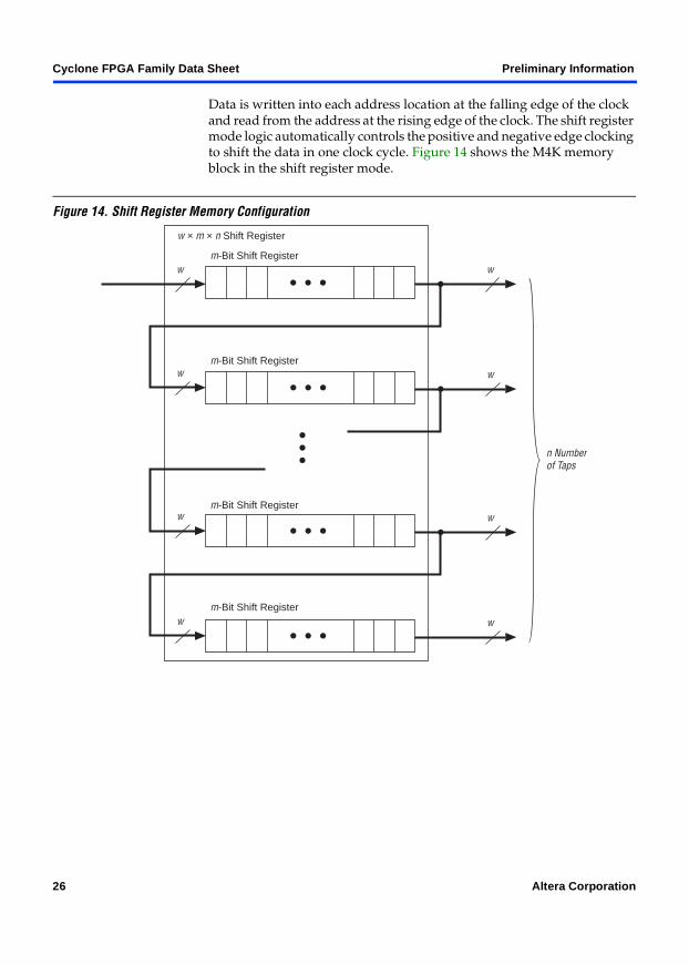
Shift Register Support
The designer can configure M4K memory blocks to implement shift registers for DSP applications such as pseudo-random number generators, multi-channel filtering, auto-correlation, and cross-correlation functions. These and other DSP applications require local data storage, traditionally implemented with standard flip-flops, which can quickly consume many logic cells and routing resources for large shift registers. A more efficient alternative is to use embedded memory as a shift register block, which saves logic cell and routing resources and provides a more efficient implementation with the dedicated circuitry.
The size of a w × m × n shift register is determined by the input data width (w), the length of the taps (m), and the number of taps (n). The size of a w × m × n shift register must be less than or equal to the maximum number of memory bits in the M4K block (4,608 bits). The total number of shift register outputs (number of taps n × width w) must be less than the maximum data width of the M4K RAM block (×36). To create larger shift registers, multiple memory blocks are cascaded together.
Altera Corporation 25
Cyclone FPGA Family Data Sheet Preliminary Information
Data is written into each address location at the falling edge of the clock and read from the address at the rising edge of the clock. The shift register mode logic automatically controls the positive and negative edge clocking to shift the data in one clock cycle. Figure 14 shows the M4K memory block in the shift register mode.
Figure 14. Shift Register Memory Configuration
m-Bit Shift Registerw w
m-Bit Shift Register
m-Bit Shift Register
m-Bit Shift Register
w w
w w
w w
w × m × n Shift Register
n Numberof Taps
26 Altera Corporation

Preliminary Information Cyclone FPGA Family Data Sheet
Memory Configuration Sizes
The memory address depths and output widths can be configured as 4,096 × 1, 2,048 × 2, 1,024 × 4, 512 × 8 (or 512 × 9 bits), 256 × 16 (or 256 × 18 bits), and 128 x 32 (or 128 x 36 bits). The 128 x 32- or 36-bit configuration is not available in the true dual-port mode. Mixed-width configurations are also possible, allowing different read and write widths. Tables 6 and 7 summarize the possible M4K RAM block configurations.
When the M4K RAM block is configured as a shift register block, the designer can create a shift register up to 4,608 bits (w × m × n).
Table 6. M4K RAM Block Configurations (Simple Dual-Port)
Read Port Write Port
4K × 1 2K × 2 1K × 4 512 × 8 256 × 16 128 × 32 512 × 9 256 × 18 128 × 36
4K × 1 v v v v v v
2K × 2 v v v v v v
1K × 4 v v v v v v
512 × 8 v v v v v v
256 × 16 v v v v v v
128 × 32 v v v v v v
512 × 9 v v v
256 × 18 v v v
128 × 36 v v v
Table 7. M4K RAM Block Configurations (True Dual-Port)
Port A Port B
4K × 1 2K × 2 1K × 4 512 × 8 256 × 16 512 × 9 256 × 18
4K × 1 v v v v v
2K × 2 v v v v v
1K × 4 v v v v v
512 × 8 v v v v v
256 × 16 v v v v v
512 × 9 v v
256 × 18 v v
Altera Corporation 27

Cyclone FPGA Family Data Sheet Preliminary Information
Byte Enables
M4K blocks support byte writes when the write port has a data width of 16, 18, 32, or 36 bits. The byte enables allow the input data to be masked so the device can write to specific bytes. The unwritten bytes retain the previous written value. Table 8 summarizes the byte selection.
Notes to Table 8:(1) Any combination of byte enables is possible.(2) Byte enables can be used in the same manner with 8-bit words, i.e., in ×16 and ×32
modes.
Control Signals & M4K Interface
The M4K blocks allow for different clocks on their inputs and outputs. Either of the two clocks feeding the block can clock M4K block registers (renwe, address, byte enable, datain, and output registers). Only the output register can be bypassed. The six labclk signals or local interconnects can drive the control signals for the A and B ports of the M4K block. LEs can also control the clock_a, clock_b, renwe_a, renwe_b, clr_a, clr_b, clocken_a, and clocken_b signals, as shown in Figure 15.
The R4, C4, and direct link interconnects from adjacent LABs drive the M4K block local interconnect. The M4K blocks can communicate with LABs on either the left or right side through these row resources or with LAB columns on either the right or left with the column resources. Up to 10 direct link input connections to the M4K block are possible from the left adjacent LABs and another 10 possible from the right adjacent LAB. M4K block outputs can also connect to left and right LABs through 10 direct link interconnects each. Figure 16 shows the M4K block to logic array interface.
Table 8. Byte Enable for M4K Blocks Notes (1), (2)
byteena[3..0] datain ×18 datain ×36
[0] = 1 [8..0] [8..0]
[1] = 1 [17..9] [17..9]
[2] = 1 – [26..18]
[3] = 1 – [35..27]
28 Altera Corporation

Preliminary Information Cyclone FPGA Family Data Sheet
Figure 15. M4K RAM Block Control Signals
Figure 16. M4K RAM Block LAB Row Interface
clocken_a
renwe_aclock_a
alcr_a
alcr_b
renwe_b
DedicatedLAB RowClocks
LocalInterconnect
LocalInterconnect
LocalInterconnect
LocalInterconnect
LocalInterconnect
clocken_b
clock_b
6
LocalInterconnect
LocalInterconnect
LocalInterconnect
LocalInterconnect
LocalInterconnect
dataout
M4K RAMBlock
datainaddress
10
Direct link interconnectfrom adjacent LAB
Direct link interconnectto adjacent LAB
Direct link interconnectfrom adjacent LAB
Direct link interconnectto adjacent LAB
M4K RAM Block LocalInterconnect Region
C4 Interconnects R4 Interconnects
LAB Row Clocks
Clocks
Byte enable
ControlSignals
6
Altera Corporation 29

Cyclone FPGA Family Data Sheet Preliminary Information
Independent Clock Mode
The M4K memory blocks implement independent clock mode for true dual-port memory. In this mode, a separate clock is available for each port (ports A and B). Clock A controls all registers on the port A side, while clock B controls all registers on the port B side. Each port, A and B, also supports independent clock enables and asynchronous clear signals for port A and B registers. Figure 17 shows an M4K memory block in independent clock mode.
Figure 17. Independent Clock Mode Note (1)
Note to Figure 17:(1) All registers shown have asynchronous clear ports.
Input/Output Clock Mode
Input/output clock mode can be implemented for both the true and simple dual-port memory modes. On each of the two ports, A or B, one clock controls all registers for inputs into the memory block: data input, wren, and address. The other clock controls the block’s data output registers. Each memory block port, A or B, also supports independent clock enables and asynchronous clear signals for input and output registers. Figures 18 and 19 show the memory block in input/output clock mode.
6D
ENA
Q
D
ENA
Q
D
ENA
Q
dataA[ ]
addressA[ ]
Memory Block256 ´ 16 (2)
512 ´ 81,024 ´ 42,048 ´ 24,096 ´ 1
Data In
Address A
Write/ReadEnable
Data Out
Data In
Address B
Write/ReadEnable
Data Out
clkenA
clockA
D
ENA
Q
wrenA
6 LAB Row Clocks
qA[ ]
6dataB[ ]
addressB[ ]
clkenB
clockB
wrenB
qB[ ]
ENA
A B
ENA
DQ
D
ENA
QbyteenaA[ ] Byte Enable A Byte Enable B byteenaB[ ]
ENA
DQ
ENA
DQ
ENA
DQ
DQ
WritePulse
Generator
WritePulse
Generator
30 Altera Corporation

Preliminary Information Cyclone FPGA Family Data Sheet
Figure 18. Input/Output Clock Mode in True Dual-Port Mode Note (1)
Note to Figure 18:(1) All registers shown have asynchronous clear ports.
6
D
ENA
Q
D
ENA
Q
D
ENA
Q
dataA[ ]
addressA[ ]
Memory Block256 × 16 (2)
512 × 81,024 × 42,048 × 24,096 × 1
Data In
Address A
Write/ReadEnable
Data Out
Data In
Address B
Write/ReadEnable
Data Out
clkenA
clockA
D
ENA
Q
wrenA
6 LAB Row Clocks
qA[ ]
6
dataB[ ]
addressB[ ]
clkenB
clockB
wrenB
qB[ ]
ENA
A B
ENA
DQ
ENA
DQ
ENA
DQ
DQ
D
ENA
QbyteenaA[ ] Byte Enable A Byte Enable B byteenaB[ ]
ENA
DQ
WritePulse
Generator
WritePulse
Generator
Altera Corporation 31

Cyclone FPGA Family Data Sheet Preliminary Information
Figure 19. Input/Output Clock Mode in Simple Dual-Port Mode Note (1)
Note to Figures 19:(1) All registers shown except the rden register have asynchronous clear ports.
Read/Write Clock Mode
The M4K memory blocks implement read/write clock mode for simple dual-port memory. The designer can use up to two clocks in this mode. The write clock controls the block’s data inputs, wraddress, and wren. The read clock controls the data output, rdaddress, and rden. The memory blocks support independent clock enables for each clock and asynchronous clear signals for the read- and write-side registers. Figure 20 shows a memory block in read/write clock mode.
6
DENA
Q
D
ENA
Q
D
ENA
Q
D
ENA
Q
DENA
Q
data[ ]
DENA
Qwraddress[ ]
address[ ]
Memory Block256 ´ 16512 ´ 8
1,024 ´ 42,048 ´ 24,096 ´ 1
Data In
Read Address
Write Address
Write Enable
Read Enable
Data Out
outclken
inclken
inclock
outclock
wren
rden
6 LAB Row Clocks
To MultiTrackInterconnect
DENA
Qbyteena[ ] Byte Enable
WritePulse
Generator
32 Altera Corporation

Preliminary Information Cyclone FPGA Family Data Sheet
Figure 20. Read/Write Clock Mode in Simple Dual-Port Mode Note (1)
Note to Figure 20:(1) All registers shown except the rden register have asynchronous clear ports.
Single-Port Mode
The M4K memory blocks also support single-port mode, used when simultaneous reads and writes are not required. See Figure 21. A single M4K memory block can support up to two single-port mode RAM blocks if each RAM block is less than or equal to 2K bits in size.
6
DENA
Q
D
ENA
Q
D
ENA
Q
D
ENA
Q
DENA
Q
data[ ]
DENA
Qwraddress[ ]
address[ ]
Memory Block256 × 16512 × 8
1,024 × 42,048 × 24,096 × 1
Data In
Read Address
Write Address
Write Enable
Read Enable
Data Out
rdclken
wrclken
wrclock
rdclock
wren
rden
6 LAB RowClocks
To MultiTrackInterconnect
DENA
Qbyteena[ ] Byte Enable
WritePulse
Generator
Altera Corporation 33

Cyclone FPGA Family Data Sheet Preliminary Information
Figure 21. Single-Port Mode
Global Clock Network & Phase-Locked Loops
Cyclone devices provide a global clock network and up to two PLLs for a complete clock management solution.
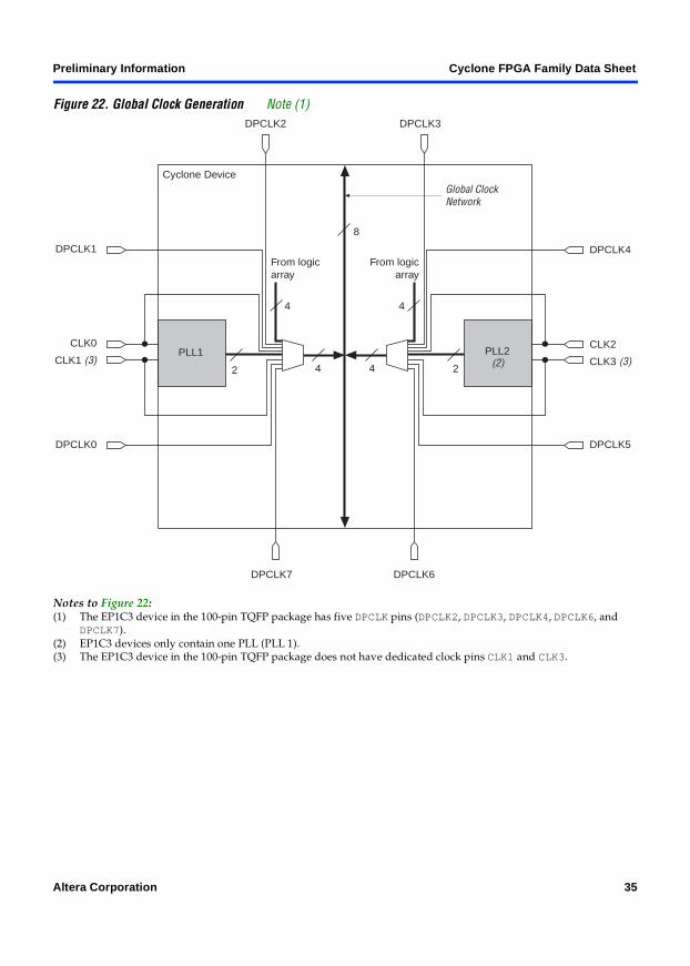
Global Clock Network
There are four dedicated clock pins (CLK[3..0], two pins on the left side and two pins on the right side) that drive the global clock network, as shown in Figure 22. PLL outputs, logic array, and dual-purpose clock (DPCLK[7..0]) pins can also drive the global clock network.
The eight global clock lines in the global clock network drive throughout the entire device. The global clock network can provide clocks for all resources within the device IOEs, LEs, and memory blocks. The global clock lines can also be used for control signals, such as clock enables and synchronous or asynchronous clears fed from the external pin, or DQS signals for DDR SDRAM or FCRAM interfaces. Internal logic can also drive the global clock network for internally generated global clocks and asynchronous clears, clock enables, or other control signals with large fanout. Figure 22 shows the various sources that drive the global clock network.
6
DENA
Q
D
ENA
Q
D
ENA
Q
DENA
Q
data[ ]
address[ ]
RAM/ROM256 × 16
512 × 81,024 × 42,048 × 24,096 × 1
Data In
Address
Write Enable
Data Out
outclken
inclken
inclock
outclock
WritePulse
Generator
wren
6 LAB RowClocks
To MultiTrackInterconnect
34 Altera Corporation
Preliminary Information Cyclone FPGA Family Data Sheet
Figure 22. Global Clock Generation Note (1)
Notes to Figure 22:(1) The EP1C3 device in the 100-pin TQFP package has five DPCLK pins (DPCLK2, DPCLK3, DPCLK4, DPCLK6, and
DPCLK7).(2) EP1C3 devices only contain one PLL (PLL 1).(3) The EP1C3 device in the 100-pin TQFP package does not have dedicated clock pins CLK1 and CLK3.
8
Global ClockNetwork
PLL1 PLL2(2)
CLK0
CLK1 (3)CLK2
CLK3 (3)
DPCLK1
DPCLK0
DPCLK4
DPCLK5
DPCLK2 DPCLK3
DPCLK7 DPCLK6
2 2
From logicarray
From logicarray
4
4 4
4
Cyclone Device
Altera Corporation 35
Cyclone FPGA Family Data Sheet Preliminary Information
Dual-Purpose Clock Pins
Each Cyclone device except the EP1C3 device has eight dual-purpose clock pins, DPCLK[7..0] (two on each I/O bank). EP1C3 devices have five DPCLK pins in the 100-pin TQFP package. These dual-purpose pins can connect to the global clock network (see Figure 22) for high-fanout control signals such as clocks, asynchronous clears, presets, and clock enables, or protocol control signals such as TRDY and IRDY for PCI, or DQS signals for external memory interfaces.
Combined Resources
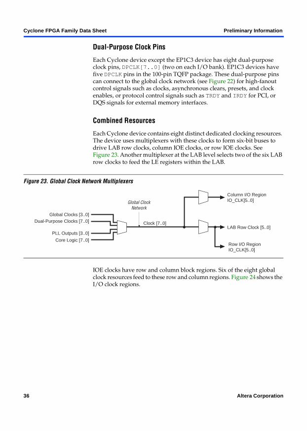
Each Cyclone device contains eight distinct dedicated clocking resources. The device uses multiplexers with these clocks to form six-bit buses to drive LAB row clocks, column IOE clocks, or row IOE clocks. See Figure 23. Another multiplexer at the LAB level selects two of the six LAB row clocks to feed the LE registers within the LAB.
Figure 23. Global Clock Network Multiplexers
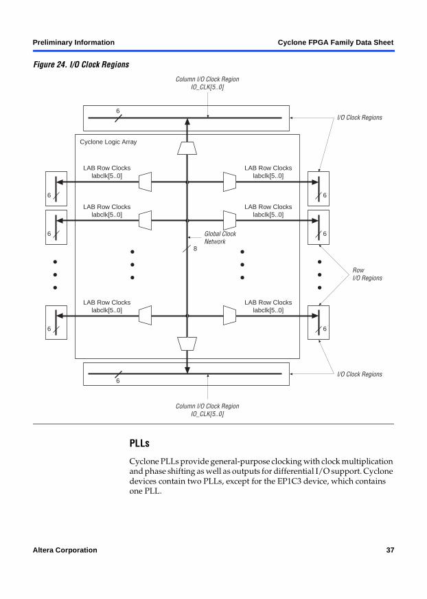
IOE clocks have row and column block regions. Six of the eight global clock resources feed to these row and column regions. Figure 24 shows the I/O clock regions.
Clock [7..0]
Column I/O RegionIO_CLK]5..0]
LAB Row Clock [5..0]
Row I/O RegionIO_CLK[5..0]
Global Clocks [3..0]
PLL Outputs [3..0]
Dual-Purpose Clocks [7..0]
Global ClockNetwork
Core Logic [7..0]
36 Altera Corporation
Preliminary Information Cyclone FPGA Family Data Sheet
Figure 24. I/O Clock Regions
PLLs
Cyclone PLLs provide general-purpose clocking with clock multiplication and phase shifting as well as outputs for differential I/O support. Cyclone devices contain two PLLs, except for the EP1C3 device, which contains one PLL.
Column I/O Clock RegionIO_CLK[5..0]
Column I/O Clock RegionIO_CLK[5..0]
6
6
I/O Clock Regions
I/O Clock Regions
8
Global ClockNetwork
RowI/O Regions
Cyclone Logic Array
6
6
LAB Row Clockslabclk[5..0]
LAB Row Clockslabclk[5..0]
LAB Row Clockslabclk[5..0]
LAB Row Clockslabclk[5..0]
LAB Row Clockslabclk[5..0]
LAB Row Clockslabclk[5..0]
6
6
6
6
Altera Corporation 37

Cyclone FPGA Family Data Sheet Preliminary Information
Table 9 shows the PLL features in Cyclone devices. Figure 25 shows a Cyclone PLL.
Notes to Table 9:(1) The m counter ranges from 2 to 32. The n counter and the post-scale counters range
from 1 to 32.(2) The smallest phase shift is determined by the voltage-controlled oscillator (VCO)
period divided by 8.(3) For degree increments, Cyclone devices can shift all output frequencies in
increments of 45°. Smaller degree increments are possible depending on the frequency and divide parameters.
(4) The EP1C3 device in the 100-pin TQFP package does not support external clock output. The EP1C6 device in the 144-pin TQFP package does not support external clock output from PLL2.
Figure 25. Cyclone PLL Note (1)
Notes to Figure 25:(1) The EP1C3 device in the 100-pin TQFP package does not support external outputs or LVDS inputs. The EP1C6
device in the 144-pin TQFP package does not support external output from PLL2.(2) LVDS input is supported via the secondary function of the dedicated clock pins. For PLL 1, the CLK0 pin’s
secondary function is LVDSCLK1p and the CLK1 pin’s secondary function is LVDSCLK1n. For PLL 2, the CLK2 pin’s secondary function is LVDSCLK2p and the CLK3 pin’s secondary function is LVDSCLK2n.
(3) PFD: phase frequency detector.
Figure 26 shows the PLL global clock connections.
Table 9. Cyclone PLL Features
Feature PLL Support
Clock multiplication and division m/(n × post-scale counter) (1)
Phase shift Down to 156-ps increments (2), (3)
Programmable duty cycle Yes
Number of internal clock outputs 2
Number of external clock outputs One differential or one single-ended (4)
ChargePump
VCOPFD (3) LoopFilter
CLK0 orLVDSCLK1p (2)
CLK1 orLVDSCLK1n (2)
÷n
÷m
∆t
∆t
Global clock
Global clock
I/O buffer
÷g0
÷g1
÷e
VCO Phase SelectionSelectable at Each PLL
Output Port
Post-ScaleCounters
38 Altera Corporation

Preliminary Information Cyclone FPGA Family Data Sheet
Figure 26. Cyclone PLL Global Clock Connections
Notes to Figure 26:(1) PLL 1 supports one single-ended or LVDS input via pins CLK0 and CLK1.(2) PLL2 supports one single-ended or LVDS input via pins CLK2 and CLK3.(3) PLL1_OUT and PLL2_OUT support single-ended or LVDS output. If external output is not required, these pins are
available as regular user I/O pins.(4) The EP1C3 device in the 100-pin TQFP package does not support external clock output. The EP1C6 device in the
144-pin TQFP package does not support external clock output from PLL2.
CLK0
CLK1 (1)PLL1 PLL2
g0
g1
e
g0
g1
e
PLL1_OUT (3), (4)
CLK2
CLK3 (2)
PLL2_OUT (3), (4)
G0 G2
G1 G3
G4 G6
G5 G7
Altera Corporation 39

Cyclone FPGA Family Data Sheet Preliminary Information
Table 10 shows the global clock network sources available in Cyclone devices.
Notes to Table 10:(1) EP1C3 devices only have one PLL (PLL 1).(2) EP1C3 devices in the 100-pin TQFP package do not have dedicated clock pins CLK1 and CLK3.(3) EP1C3 devices in the 100-pin TQFP package do not have the DPCLK0, DPCLK1, or DPCLK5 pins.
Clock Multiplication & Division
Cyclone PLLs provide clock synthesis for PLL output ports using m/(n × post scale counter) scaling factors. The input clock is divided by a pre-scale divider, n, and is then multiplied by the m feedback factor. The control loop drives the VCO to match fIN × (m/n). Each output port has a unique post-scale counter to divide down the high-frequency VCO. For multiple PLL outputs with different frequencies, the VCO is set to the least-common multiple of the output frequencies that meets its frequency specifications. Then, the post-scale dividers scale down the output frequency for each output port. For example, if the output frequencies required from one PLL are 33 and 66 MHz, the VCO is set to 330 MHz (the least-common multiple in the VCO’s range).
Table 10. Global Clock Network Sources
Source GCLK0 GCLK1 GCLK2 GCLK3 GCLK4 GCLK5 GCLK6 GCLK7
PLL Counter Output
PLL1 G0 v v
PLL1 G1 v v
PLL2 G0 (1) v v
PLL2 G1 (1) v v
Dedicated Clock Input Pins
CLK0 v v
CLK1 (2) v v
CLK2 v v
CLK3 (2) v v
Dual-Purpose Clock Pins
DPCLK0 (3) v
DPCLK1 (3) v
DPCLK2 v
DPCLK3 v
DPCLK4 v
DPCLK5 (3) v
DPCLK6 v
DPCLK7 v
40 Altera Corporation

Preliminary Information Cyclone FPGA Family Data Sheet
Each PLL has one pre-scale divider, n, that can range in value from 1 to 32. Each PLL also has one multiply divider, m, that can range in value from 2 to 32. Global clock outputs have two post scale G dividers for global clock outputs, and external clock outputs have an E divider for external clock output, both ranging from 1 to 32. The Quartus II software automatically chooses the appropriate scaling factors according to the input frequency, multiplication, and division values entered.
External Clock Inputs
Each PLL supports single-ended or differential inputs for source-synchronous receivers or for general-purpose use. The dedicated clock pins (CLK[3..0]) feed the PLL inputs. These dual-purpose pins can also act as LVDS input pins. See Figure 25.
Table 11 shows the I/O standards supported by PLL input and output pins.
For more information on LVDS I/O support, see “LVDS I/O Pins” on page 59.
External Clock Outputs
Each PLL supports one differential or one single-ended output for source-synchronous transmitters or for general-purpose external clocks. If the PLL does not use these PLL_OUT pins, the pins are available for use as general-purpose I/O pins. The PLL_OUT pins support all I/O standards shown in Table 11.
Table 11. PLL I/O Standards
I/O Standard CLK Input EXTCLK Output
3.3-V LVTTL/LVCMOS v v
2.5-V LVTTL/LVCMOS v v
1.8-V LVTTL/LVCMOS v v
1.5-V LVCMOS v v
3.3-V PCI v v
LVDS v v
SSTL-2 class I v v
SSTL-2 class II v v
SSTL-3 class I v v
SSTL-3 class II v v
Differential SSTL-2 v
Altera Corporation 41

Cyclone FPGA Family Data Sheet Preliminary Information
The external clock outputs do not have their own VCC and ground voltage supplies. Therefore, to minimize jitter, do not place switching I/O pins next to these output pins. The EP1C3 device in the 100-pin TQFP package does not have dedicated clock output pins. The EP1C6 device in the 144-pin TQFP package only supports dedicated clock outputs from PLL 1.
Clock Feedback
Cyclone PLLs have three modes for multiplication and/or phase shifting:
Zero delay buffer mode The external clock output pin is phase-aligned with the clock input pin for zero delay.
Normal mode If the design uses an internal PLL clock output, the normal mode compensates for the internal clock delay from the input clock pin to the IOE registers. The external clock output pin is phase shifted with respect to the clock input pin if connected in this mode. The designer defines which internal clock output from the PLL should be phase-aligned to compensate for internal clock delay.
No compensation mode In this mode, the PLL will not compensate for any clock networks.
Phase Shifting
Cyclone PLLs have an advanced clock shift capability that enables programmable phase shifts. Designers can enter a phase shift (in degrees or time units) for each PLL clock output port or for all outputs together in one shift. Designers can perform phase shifting in time units with a resolution range of 156 to 417 ps. The finest resolution equals one eighth of the VCO period. The VCO period is a function of the frequency input and the multiplication and division factors. Each clock output counter can choose a different phase of the VCO period from up to eight taps. Designers can use this clock output counter along with an initial setting on the post-scale counter to achieve a phase-shift range for the entire period of the output clock. The phase tap feedback to the m counter can shift all outputs to a single phase. The Quartus II software automatically sets the phase taps and counter settings according to the phase shift entered.
Lock Detect Signal
The lock output indicates that there is a stable clock output signal in phase with the reference clock. Without any additional circuitry, the lock signal may toggle as the PLL begins tracking the reference clock. Therefore, the designer may need to gate the lock signal for use as a system-control signal.
42 Altera Corporation

Preliminary Information Cyclone FPGA Family Data Sheet
Programmable Duty Cycle
The programmable duty cycle allows PLLs to generate clock outputs with a variable duty cycle. This feature is supported on each PLL post-scale counter (g0, g1, e). The duty cycle setting is achieved by a low- and high-time count setting for the post-scale dividers. The Quartus II software uses the frequency input and the required multiply or divide rate to determine the duty cycle choices.
Control Signals
There are three control signals for clearing and enabling PLLs and their outputs. The designer can use these signals to control PLL resynchronization and the ability to gate PLL output clocks for low-power applications.
The pllenable signal enables and disables PLLs. When the pllenable signal is low, the clock output ports are driven by ground and all the PLLs go out of lock. When the pllenable signal goes high again, the PLLs relock and resynchronize to the input clocks. An input pin or LE output can drive the pllenable signal.
The areset signals are reset/resynchronization inputs for each PLL. Cyclone devices can drive these input signals from input pins or from LEs. When areset is driven high, the PLL counters will reset, clearing the PLL output and placing the PLL out of lock. When driven low again, the PLL will resynchronize to its input as it relocks.
The pfdena signals control the phase frequency detector (PFD) output with a programmable gate. If you disable the PFD, the VCO will operate at its last set value of control voltage and frequency with some drift, and the system will continue running when the PLL goes out of lock or the input clock disables. By maintaining the last locked frequency, the system has time to store its current settings before shutting down. The designer can either use their own control signal or gated locked status signals to trigger the pfdena signal.
f For more information on Cyclone PLLs, see AN 251: Using PLLs in Cyclone Devices.
Altera Corporation 43

Cyclone FPGA Family Data Sheet Preliminary Information
I/O Structure IOEs support many features, including:
Differential and single-ended I/O standards 3.3-V, 32-bit, 66-MHz PCI compliance Joint Test Action Group (JTAG) boundary-scan test (BST) support Output drive strength control Weak pull-up resistors during configuration Slew-rate control Tri-state buffers Bus-hold circuitry Programmable pull-up resistors in user mode Programmable input and output delays Open-drain outputs DQ and DQS I/O pins
Cyclone device IOEs contain a bidirectional I/O buffer and three registers for complete embedded bidirectional single data rate transfer. Figure 27 shows the Cyclone IOE structure. The IOE contains one input register, one output register, and one output enable register. The designer can use the input registers for fast setup times and output registers for fast clock-to-output times. Additionally, the designer can use the output enable (OE) register for fast clock-to-output enable timing. The Quartus II software automatically duplicates a single OE register that controls multiple output or bidirectional pins. IOEs can be used as input, output, or bidirectional pins.
44 Altera Corporation

Preliminary Information Cyclone FPGA Family Data Sheet
Figure 27. Cyclone IOE Structure
Note to Figure 27:(1) There are two paths available for combinatorial inputs to the logic array. Each path
contains a unique programmable delay chain.
The IOEs are located in I/O blocks around the periphery of the Cyclone device. There are up to three IOEs per row I/O block and up to three IOEs per column I/O block (column I/O blocks span two columns). The row I/O blocks drive row, column, or direct link interconnects. The column I/O blocks drive column interconnects. Figure 28 shows how a row I/O block connects to the logic array. Figure 29 shows how a column I/O block connects to the logic array.
Output Register
Output
Combinatorialinput (1)
Input
OE Register
OE
Input Register
Logic Array
D Q
D Q
D Q
Altera Corporation 45

Cyclone FPGA Family Data Sheet Preliminary Information
Figure 28. Row I/O Block Connection to the Interconnect
Notes to Figure 28:(1) The 21 data and control signals consist of three data out lines, io_dataout[2..0], three output enables,
io_coe[2..0], three input clock enables, io_cce_in[2..0], three output clock enables, io_cce_out[2..0], three clocks, io_cclk[2..0], three asynchronous clear signals, io_caclr[2..0], and three synchronous clear signals, io_csclr[2..0].
(2) Each of the three IOEs in the row I/O block can have one io_datain input (combinatorial or registered) and one comb_io_datain (combinatorial) input.
21
R4 Interconnects C4 Interconnects
I/O Block Local Interconnect
21 Data andControl Signalsfrom Logic Array (1)
io_datain[2..0] andcomb_io_datain[2..0] (2)
io_clk[5:0]
Row I/O BlockContains up to
Three IOEs
Direct LinkInterconnect
to Adjacent LAB
Direct LinkInterconnect
from Adjacent LAB
LAB LocalInterconnect
LAB RowI/O Block
46 Altera Corporation

Preliminary Information Cyclone FPGA Family Data Sheet
Figure 29. Column I/O Block Connection to the Interconnect
Notes to Figure 29:(1) The 21 data and control signals consist of three data out lines, io_dataout[2..0], three output enables,
io_coe[2..0], three input clock enables, io_cce_in[2..0], three output clock enables, io_cce_out[2..0], three clocks, io_cclk[2..0], three asynchronous clear signals, io_caclr[2..0], and three synchronous clear signals, io_csclr[2..0].
(2) Each of the three IOEs in the column I/O block can have one io_datain input (combinatorial or registered) and one comb_io_datain (combinatorial) input.
21 Data &Control Signals
from Logic Array (1)
Column I/O Block Containsup to Three IOEs
I/O BlockLocal Interconnect
IO_datain[2:0] &comb_io_datain[2..0]
(2)
R4 Interconnects
LAB LocalInterconnect
C4 Interconnects
21
LAB LAB LAB
io_clk[5..0]
Column I/O Block
Altera Corporation 47

Cyclone FPGA Family Data Sheet Preliminary Information
The pin’s datain signals can drive the logic array. The logic array drives the control and data signals, providing a flexible routing resource. The row or column IOE clocks, io_clk[5..0], provide a dedicated routing resource for low-skew, high-speed clocks. The global clock network generates the IOE clocks that feed the row or column I/O regions (see “Global Clock Network & Phase-Locked Loops” on page 34). Figure 30 illustrates the signal paths through the I/O block.
Figure 30. Signal Path through the I/O Block
Each IOE contains its own control signal selection for the following control signals: oe, ce_in, ce_out, aclr/preset, sclr/preset, clk_in, and clk_out. Figure 31 illustrates the control signal selection.
Row or Columnio_clk[5..0]
io_datain
comb_io_datain
io_dataout
io_coe
oe
ce_in
ce_out
io_cce_inaclr/preset
io_cce_outsclr
io_caclrclk_in
io_cclkclk_out
dataout
Data andControlSignal
Selection
IOE
To LogicArray
From LogicArray
To OtherIOEs
io_csclr
48 Altera Corporation

Preliminary Information Cyclone FPGA Family Data Sheet
Figure 31. Control Signal Selection per IOE
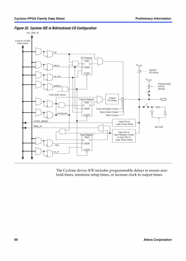
In normal bidirectional operation, the designer can use the input register for input data requiring fast setup times. The input register can have its own clock input and clock enable separate from the OE and output registers. The output register can be used for data requiring fast clock-to-output performance. The OE register is available for fast clock-to-output enable timing. The OE and output register share the same clock source and the same clock enable source from the local interconnect in the associated LAB, dedicated I/O clocks, or the column and row interconnects. Figure 32 shows the IOE in bidirectional configuration.
clk_out
ce_inclk_in
ce_out
aclr/preset
sclr/preset
Dedicated I/OClock [5..0]
LocalInterconnect
LocalInterconnect
LocalInterconnect
LocalInterconnect
LocalInterconnect
oe
io_coe
io_caclr
LocalInterconnect
io_csclr
io_cce_out
io_cce_in
io_cclk
Altera Corporation 49
Cyclone FPGA Family Data Sheet Preliminary Information
Figure 32. Cyclone IOE in Bidirectional I/O Configuration
The Cyclone device IOE includes programmable delays to ensure zero hold times, minimize setup times, or increase clock to output times.
Chip-Wide Reset
OE Register
VCCIO
OptionalPCI Clamp
Column or RowInterconect
ioe_clk[5..0]
Input RegisterInput Pin to
Input Register Delayor Input Pin to
Logic Array Delay
Input Pin toLogic Array Delay
Drive Strength Control
Open-Drain Output
Slew Controlsclr/preset
OE
clkout
ce_out
aclr/prn
clkin
ce_in
OutputPin Delay
ProgrammablePull-UpResistor
Bus Hold
PRN
CLRN
D Q
Output Register
PRN
CLRN
D Q
PRN
CLRN
D Q
VCCIO
comb_datain
data_in
ENA
ENA
ENA
50 Altera Corporation

Preliminary Information Cyclone FPGA Family Data Sheet
A path in which a pin directly drives a register may require a programmable delay to ensure zero hold time, whereas a path in which a pin drives a register through combinatorial logic may not require the delay. Programmable delays decrease input-pin-to-logic-array and IOE input register delays. The Quartus II Compiler can program these delays to automatically minimize setup time while providing a zero hold time. Programmable delays can increase the register-to-pin delays for output registers. Table 12 shows the programmable delays for Cyclone devices.
There are two paths in the IOE for a combinatorial input to reach the logic array. Each of the two paths can have a different delay. This allows the designer to adjust delays from the pin to internal LE registers that reside in two different areas of the device. The designer sets the two combinatorial input delays by selecting different delays for two different paths under the Decrease input delay to internal cells logic option in the Quartus II software. When the input signal requires two different delays for the combinatorial input, the input register in the IOE is no longer available.
The IOE registers in Cyclone devices share the same source for clear or preset. The designer can program preset or clear for each individual IOE. The designer can also program the registers to power up high or low after configuration is complete. If programmed to power up low, an asynchronous clear can control the registers. If programmed to power up high, an asynchronous preset can control the registers. This feature prevents the inadvertent activation of another device’s active-low input upon power up. If one register in an IOE uses a preset or clear signal then all registers in the IOE must use that same signal if they require preset or clear. Additionally a synchronous reset signal is available to the designer for the IOE registers.
External RAM Interfacing
Cyclone devices support DDR SDRAM and FCRAM interfaces at up to 133 MHz through dedicated circuitry.
Table 12. Cyclone Programmable Delay Chain
Programmable Delays Quartus II Logic Option
Input pin to logic array delay Decrease input delay to internal cells
Input pin to input register delay Decrease input delay to input registers
Output pin delay Increase delay to output pin
Altera Corporation 51
Cyclone FPGA Family Data Sheet Preliminary Information
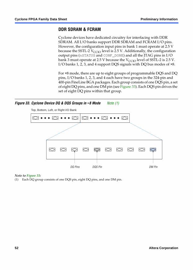
DDR SDRAM & FCRAM
Cyclone devices have dedicated circuitry for interfacing with DDR SDRAM. All I/O banks support DDR SDRAM and FCRAM I/O pins. However, the configuration input pins in bank 1 must operate at 2.5 V because the SSTL-2 VCCIO level is 2.5 V. Additionally, the configuration output pins (nSTATUS and CONF_DONE) and all the JTAG pins in I/O bank 3 must operate at 2.5 V because the VCCIO level of SSTL-2 is 2.5 V. I/O banks 1, 2, 3, and 4 support DQS signals with DQ bus modes of ×8.
For ×8 mode, there are up to eight groups of programmable DQS and DQ pins, I/O banks 1, 2, 3, and 4 each have two groups in the 324-pin and 400-pin FineLine BGA packages. Each group consists of one DQS pin, a set of eight DQ pins, and one DM pin (see Figure 33). Each DQS pin drives the set of eight DQ pins within that group.
Figure 33. Cyclone Device DQ & DQS Groups in ×8 Mode Note (1)
Note to Figure 33:(1) Each DQ group consists of one DQS pin, eight DQ pins, and one DM pin.
DQ Pins DQS Pin DM Pin
Top, Bottom, Left, or Right I/O Bank
52 Altera Corporation
Preliminary Information Cyclone FPGA Family Data Sheet
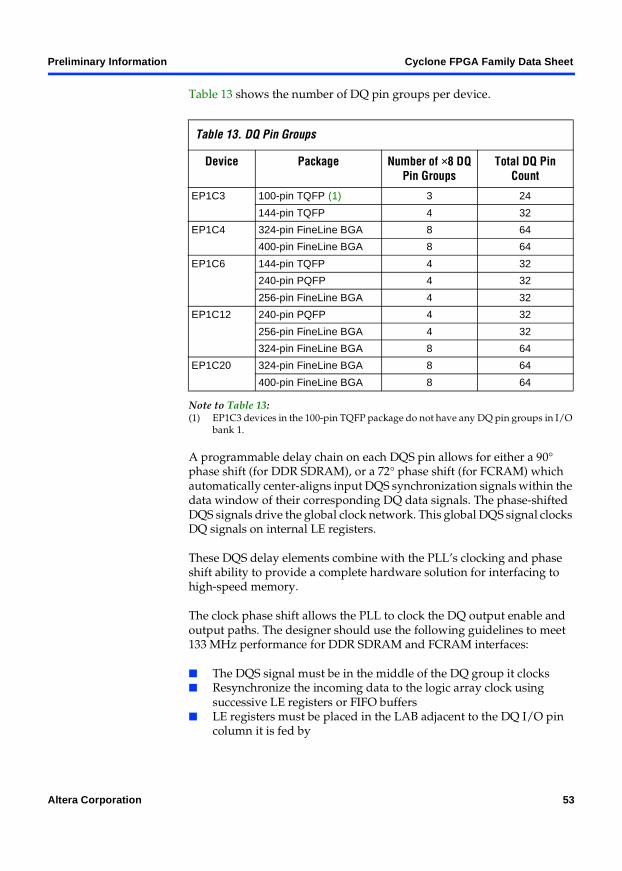
Table 13 shows the number of DQ pin groups per device.
Note to Table 13:(1) EP1C3 devices in the 100-pin TQFP package do not have any DQ pin groups in I/O
bank 1.
A programmable delay chain on each DQS pin allows for either a 90° phase shift (for DDR SDRAM), or a 72° phase shift (for FCRAM) which automatically center-aligns input DQS synchronization signals within the data window of their corresponding DQ data signals. The phase-shifted DQS signals drive the global clock network. This global DQS signal clocks DQ signals on internal LE registers.
These DQS delay elements combine with the PLL’s clocking and phase shift ability to provide a complete hardware solution for interfacing to high-speed memory.
The clock phase shift allows the PLL to clock the DQ output enable and output paths. The designer should use the following guidelines to meet 133 MHz performance for DDR SDRAM and FCRAM interfaces:
The DQS signal must be in the middle of the DQ group it clocks Resynchronize the incoming data to the logic array clock using
successive LE registers or FIFO buffers LE registers must be placed in the LAB adjacent to the DQ I/O pin
column it is fed by
Table 13. DQ Pin Groups
Device Package Number of ×8 DQ Pin Groups
Total DQ Pin Count
EP1C3 100-pin TQFP (1) 3 24
144-pin TQFP 4 32
EP1C4 324-pin FineLine BGA 8 64
400-pin FineLine BGA 8 64
EP1C6 144-pin TQFP 4 32
240-pin PQFP 4 32
256-pin FineLine BGA 4 32
EP1C12 240-pin PQFP 4 32
256-pin FineLine BGA 4 32
324-pin FineLine BGA 8 64
EP1C20 324-pin FineLine BGA 8 64
400-pin FineLine BGA 8 64
Altera Corporation 53

Cyclone FPGA Family Data Sheet Preliminary Information
Figure 34 illustrates DDR SDRAM and FCRAM interfacing from the I/O through the dedicated circuitry to the logic array.
Figure 34. DDR SDRAM & FCRAM Interfacing
VCC
GND
PLL
Phase Shifted -90˚
DQS
Adjacent LAB LEs
Global Clock
ResynchronizingGlobal Clock
ProgrammableDelay Chain
Output LERegister
Output LERegisters
DQ
Input LERegisters
Input LERegisters
LERegister
LERegister
∆ t
AdjacentLAB LEs
OE OE LERegister
OE LERegister
OE OE LERegister
OE LERegister
Output LERegisters
Output LERegister
DataA
DataB
clk
-90˚ clk
54 Altera Corporation

Preliminary Information Cyclone FPGA Family Data Sheet
Programmable Drive Strength
The output buffer for each Cyclone device I/O pin has a programmable drive strength control for certain I/O standards. The LVTTL and LVCMOS standards have several levels of drive strength that the designer can control. SSTL-3 class I and II, and SSTL-2 class I and II support a minimum setting, the lowest drive strength that guarantees the IOH/IOL of the standard. Using minimum settings provides signal slew rate control to reduce system noise and signal overshoot. Table 14 shows the possible settings for the I/O standards with drive strength control.
Open-Drain Output
Cyclone devices provide an optional open-drain (equivalent to an open-collector) output for each I/O pin. This open-drain output enables the device to provide system-level control signals (e.g., interrupt and write-enable signals) that can be asserted by any of several devices.
Table 14. Programmable Drive Strength
I/O Standard IOH/IOL Current Strength Setting (mA)
LVTTL (3.3 V) 4
8
12
16
24
LVCMOS (3.3 V) 2
4
8
12
LVTTL (2.5 V) 2
8
12
16
LVTTL (1.8 V) 2
8
12
LVCMOS (1.5 V) 2
4
8
Altera Corporation 55

Cyclone FPGA Family Data Sheet Preliminary Information
Slew-Rate Control
The output buffer for each Cyclone device I/O pin has a programmable output slew-rate control that can be configured for low noise or high-speed performance. A faster slew rate provides high-speed transitions for high-performance systems. However, these fast transitions may introduce noise transients into the system. A slow slew rate reduces system noise, but adds a nominal delay to rising and falling edges. Each I/O pin has an individual slew-rate control, allowing the designer to specify the slew rate on a pin-by-pin basis. The slew-rate control affects both the rising and falling edges.
Bus Hold
Each Cyclone device I/O pin provides an optional bus-hold feature. The bus-hold circuitry can hold the signal on an I/O pin at its last-driven state. Since the bus-hold feature holds the last-driven state of the pin until the next input signal is present, an external pull-up or pull-down resistor is not necessary to hold a signal level when the bus is tri-stated.
The bus-hold circuitry also pulls undriven pins away from the input threshold voltage where noise can cause unintended high-frequency switching. The designer can select this feature individually for each I/O pin. The bus-hold output will drive no higher than VCCIO to prevent overdriving signals. If the bus-hold feature is enabled, the device cannot use the programmable pull-up option. Disable the bus-hold feature when the I/O pin is configured for differential signals.
The bus-hold circuitry uses a resistor with a nominal resistance (RBH) of approximately 7 kΩ to pull the signal level to the last-driven state. Table 37 on page 72 gives the specific sustaining current for each VCCIO voltage level driven through this resistor and overdrive current used to identify the next-driven input level.
The bus-hold circuitry is only active after configuration. When going into user mode, the bus-hold circuit captures the value on the pin present at the end of configuration.
Programmable Pull-Up Resistor
Each Cyclone device I/O pin provides an optional programmable pull-up resistor during user mode. If the designer enables this feature for an I/O pin, the pull-up resistor (typically 25 kΩ) holds the output to the VCCIO level of the output pin’s bank.
56 Altera Corporation

Preliminary Information Cyclone FPGA Family Data Sheet
Advanced I/O Standard Support
Cyclone device IOEs support the following I/O standards:
3.3-V LVTTL/LVCMOS 2.5-V LVTTL/LVCMOS 1.8-V LVTTL/LVCMOS 1.5-V LVCMOS 3.3-V PCI LVDS SSTL-2 class I and II SSTL-3 class I and II Differential SSTL-2 class II (on output clocks only)
Table 15 describes the I/O standards supported by Cyclone devices.
Notes to Table 15:(1) EP1C3 devices do not support PCI.(2) EP1C3 devices in the 100-pin TQFP package do not support the LVDS I/O standard.(3) This I/O standard is only available on output clock pins (PLL_OUT pins).
Cyclone devices contain four I/O banks, as shown in Figure 35. I/O banks 1 and 3 support all the I/O standards listed in Table 15. I/O banks 2 and 4 support all the I/O standards listed in Table 15 except the 3.3-V PCI standard. I/O banks 2 and 4 contain dual-purpose DQS, DQ, and DM pins to support a DDR SDRAM or FCRAM interface. I/O bank 1 can also support a DDR SDRAM or FCRAM interface, however, the configuration input pins in I/O bank 1 must operate at 2.5 V. I/O bank 3 can also support a DDR SDRAM or FCRAM interface, however, all the JTAG pins in I/O bank 3 must operate at 2.5 V.
Table 15. Cyclone I/O Standards
I/O Standard Type Input Reference Voltage (VREF) (V)
Output Supply Voltage (VCCIO)
(V)
Board Termination
Voltage (VTT) (V)
3.3-V LVTTL/LVCMOS Single-ended N/A 3.3 N/A
2.5-V LVTTL/LVCMOS Single-ended N/A 2.5 N/A
1.8-V LVTTL/LVCMOS Single-ended N/A 1.8 N/A
1.5-V LVCMOS Single-ended N/A 1.5 N/A
3.3-V PCI (1) Single-ended N/A 3.3 N/A
LVDS (2) Differential N/A 2.5 N/A
SSTL-2 class I and II Voltage-referenced 1.25 2.5 1.25
SSTL-3 class I and II Voltage-referenced 1.5 3.3 1.5
Differential SSTL-2 (3) Differential 1.25 2.5 1.25
Altera Corporation 57
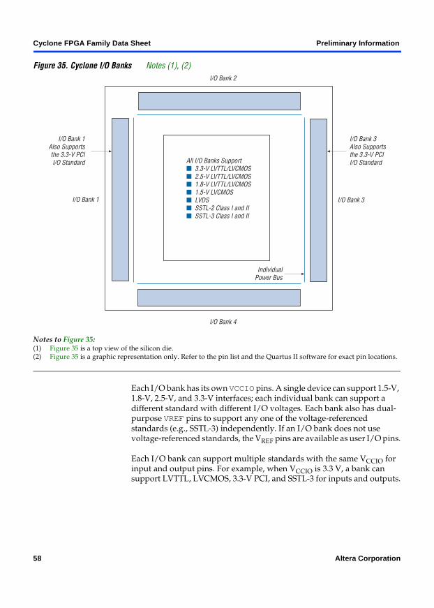
Cyclone FPGA Family Data Sheet Preliminary Information
Figure 35. Cyclone I/O Banks Notes (1), (2)
Notes to Figure 35:(1) Figure 35 is a top view of the silicon die.(2) Figure 35 is a graphic representation only. Refer to the pin list and the Quartus II software for exact pin locations.
Each I/O bank has its own VCCIO pins. A single device can support 1.5-V, 1.8-V, 2.5-V, and 3.3-V interfaces; each individual bank can support a different standard with different I/O voltages. Each bank also has dual-purpose VREF pins to support any one of the voltage-referenced standards (e.g., SSTL-3) independently. If an I/O bank does not use voltage-referenced standards, the VREF pins are available as user I/O pins.
Each I/O bank can support multiple standards with the same VCCIO for input and output pins. For example, when VCCIO is 3.3 V, a bank can support LVTTL, LVCMOS, 3.3-V PCI, and SSTL-3 for inputs and outputs.
I/O Bank 2
I/O Bank 3
I/O Bank 4
I/O Bank 1
All I/O Banks Support 3.3-V LVTTL/LVCMOS 2.5-V LVTTL/LVCMOS 1.8-V LVTTL/LVCMOS 1.5-V LVCMOS LVDS SSTL-2 Class I and II SSTL-3 Class I and II
I/O Bank 3Also Supportsthe 3.3-V PCII/O Standard
I/O Bank 1Also Supportsthe 3.3-V PCII/O Standard
IndividualPower Bus
58 Altera Corporation
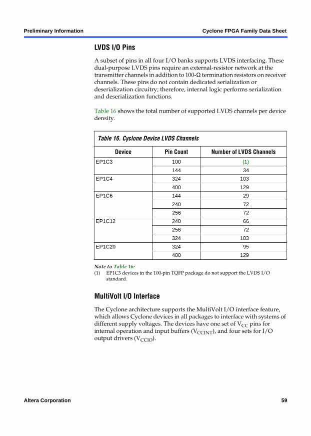
Preliminary Information Cyclone FPGA Family Data Sheet
LVDS I/O Pins
A subset of pins in all four I/O banks supports LVDS interfacing. These dual-purpose LVDS pins require an external-resistor network at the transmitter channels in addition to 100-Ω termination resistors on receiver channels. These pins do not contain dedicated serialization or deserialization circuitry; therefore, internal logic performs serialization and deserialization functions.
Table 16 shows the total number of supported LVDS channels per device density.
Note to Table 16:(1) EP1C3 devices in the 100-pin TQFP package do not support the LVDS I/O
standard.
MultiVolt I/O Interface
The Cyclone architecture supports the MultiVolt I/O interface feature, which allows Cyclone devices in all packages to interface with systems of different supply voltages. The devices have one set of VCC pins for internal operation and input buffers (VCCINT), and four sets for I/O output drivers (VCCIO).
Table 16. Cyclone Device LVDS Channels
Device Pin Count Number of LVDS Channels
EP1C3 100 (1)
144 34
EP1C4 324 103
400 129
EP1C6 144 29
240 72
256 72
EP1C12 240 66
256 72
324 103
EP1C20 324 95
400 129
Altera Corporation 59
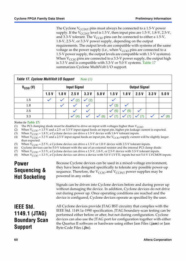
Cyclone FPGA Family Data Sheet Preliminary Information
The Cyclone VCCINT pins must always be connected to a 1.5-V power supply. If the VCCINT level is 1.5 V, then input pins are 1.5-V, 1.8-V, 2.5-V, and 3.3-V tolerant. The VCCIO pins can be connected to either a 1.5-V, 1.8-V, 2.5-V, or 3.3-V power supply, depending on the output requirements. The output levels are compatible with systems of the same voltage as the power supply (i.e., when VCCIO pins are connected to a 1.5-V power supply, the output levels are compatible with 1.5-V systems). When VCCIO pins are connected to a 3.3-V power supply, the output high is 3.3 V and is compatible with 3.3-V or 5.0-V systems. Table 17 summarizes Cyclone MultiVolt I/O support.
Notes to Table 17:(1) The PCI clamping diode must be disabled to drive an input with voltages higher than VCCIO.(2) When VCCIO = 1.5 V and a 2.5- or 3.3-V input signal feeds an input pin, higher pin leakage current is expected.(3) When VCCIO = 1.8 V, a Cyclone device can drive a 1.5-V device with 1.8-V tolerant inputs.(4) When VCCIO = 3.3 V and a 2.5-V input signal feeds an input pin, the VCCIO supply current will be slightly larger
than expected.(5) When VCCIO = 2.5 V, a Cyclone device can drive a 1.5-V or 1.8-V device with 2.5-V tolerant inputs.(6) Cyclone devices can be 5.0-V tolerant with the use of an external resistor and the internal PCI clamp diode.(7) When VCCIO = 3.3 V, a Cyclone device can drive a 1.5-V, 1.8-V, or 2.5-V device with 3.3-V tolerant inputs.(8) When VCCIO = 3.3 V, a Cyclone device can drive a device with 5.0-V LVTTL inputs but not 5.0-V LVCMOS inputs.
Power Sequencing & Hot Socketing
Because Cyclone devices can be used in a mixed-voltage environment, they have been designed specifically to tolerate any possible power-up sequence. Therefore, the VCCIO and VCCINT power supplies may be powered in any order.
Signals can be driven into Cyclone devices before and during power up without damaging the device. In addition, Cyclone devices do not drive out during power up. Once operating conditions are reached and the device is configured, Cyclone devices operate as specified by the user.
IEEE Std. 1149.1 (JTAG) Boundary Scan Support
All Cyclone devices provide JTAG BST circuitry that complies with the IEEE Std. 1149.1a-1990 specification. JTAG boundary-scan testing can be performed either before or after, but not during configuration. Cyclone devices can also use the JTAG port for configuration together with either the Quartus II software or hardware using either Jam Files (.jam) or Jam Byte-Code Files (.jbc).
Table 17. Cyclone MultiVolt I/O Support Note (1)
VCCIO (V) Input Signal Output Signal
1.5 V 1.8 V 2.5 V 3.3 V 5.0 V 1.5 V 1.8 V 2.5 V 3.3 V 5.0 V
1.5 v v v (2) v (2) v
1.8 v v v v (3) v
2.5 v v v (5) v (5) v
3.3 v (4) v v (6) v (7) v (7) v (7) v v (8)
60 Altera Corporation

Preliminary Information Cyclone FPGA Family Data Sheet
Cyclone devices support reconfiguring the I/O standard settings on the IOE through the JTAG BST chain. The JTAG chain can update the I/O standard for all input and output pins any time before or during user mode. Designers can use this ability for JTAG testing before configuration when some of the Cyclone pins drive or receive from other devices on the board using voltage-referenced standards. Since the Cyclone device might not be configured before JTAG testing, the I/O pins might not be configured for appropriate electrical standards for chip-to-chip communication. Programming those I/O standards via JTAG allows designers to fully test I/O connection to other devices.
The JTAG pins support 1.5-V/1.8-V or 2.5-V/3.3-V I/O standards. The TDO pin voltage is determined by the VCCIO of the bank where it resides. The bank VCCIO selects whether the JTAG inputs are 1.5-V, 1.8-V, 2.5-V, or 3.3-V compatible.
Cyclone devices also use the JTAG port to monitor the operation of the device with the SignalTap II embedded logic analyzer. Cyclone devices support the JTAG instructions shown in Table 18.
Altera Corporation 61

Cyclone FPGA Family Data Sheet Preliminary Information
Note to Table 18:(1) Bus hold and weak pull-up resistor features override the high-impedance state of HIGHZ, CLAMP, and EXTEST.
Table 18. Cyclone JTAG Instructions
JTAG Instruction Instruction Code Description
SAMPLE/PRELOAD 00 0000 0101 Allows a snapshot of signals at the device pins to be captured and examined during normal device operation, and permits an initial data pattern to be output at the device pins. Also used by the SignalTap II embedded logic analyzer.
EXTEST (1) 00 0000 0000 Allows the external circuitry and board-level interconnects to be tested by forcing a test pattern at the output pins and capturing test results at the input pins.
BYPASS 11 1111 1111 Places the 1-bit bypass register between the TDI and TDO pins, which allows the BST data to pass synchronously through selected devices to adjacent devices during normal device operation.
USERCODE 00 0000 0111 Selects the 32-bit USERCODE register and places it between the TDI and TDO pins, allowing the USERCODE to be serially shifted out of TDO.
IDCODE 00 0000 0110 Selects the IDCODE register and places it between TDI and TDO, allowing the IDCODE to be serially shifted out of TDO.
HIGHZ (1) 00 0000 1011 Places the 1-bit bypass register between the TDI and TDO pins, which allows the BST data to pass synchronously through selected devices to adjacent devices during normal device operation, while tri-stating all of the I/O pins.
CLAMP (1) 00 0000 1010 Places the 1-bit bypass register between the TDI and TDO pins, which allows the BST data to pass synchronously through selected devices to adjacent devices during normal device operation while holding I/O pins to a state defined by the data in the boundary-scan register.
ICR instructions Used when configuring a Cyclone device via the JTAG port with a MasterBlasterTM or ByteBlasterMVTM download cable, or when using a Jam File or Jam Byte-Code File via an embedded processor.
PULSE_NCONFIG 00 0000 0001 Emulates pulsing the nCONFIG pin low to trigger reconfiguration even though the physical pin is unaffected.
CONFIG_IO 00 0000 1101 Allows configuration of I/O standards through the JTAG chain for JTAG testing. Can be executed before, after, or during configuration. Stops configuration if executed during configuration. Once issued, the CONFIG_IO instruction will hold nSTATUS low to reset the configuration device. nSTATUS is held low until the device is reconfigured.
SignalTap II instructions
Monitors internal device operation with the SignalTap II embedded logic analyzer.
62 Altera Corporation

Preliminary Information Cyclone FPGA Family Data Sheet
The Cyclone device instruction register length is 10 bits and the USERCODE register length is 32 bits. Tables 19 and 20 show the boundary-scan register length and device IDCODE information for Cyclone devices.
Notes to Table 20:(1) The most significant bit (MSB) is on the left.(2) The IDCODE’s least significant bit (LSB) is always 1.
Table 19. Cyclone Boundary-Scan Register Length
Device Boundary-Scan Register Length
EP1C3 339
EP1C4 930
EP1C6 582
EP1C12 774
EP1C20 930
Table 20. 32-Bit Cyclone Device IDCODE
Device IDCODE (32 Bits) (1)
Version (4 Bits) Part Number (16 Bits) Manufacturer Identity (11 Bits)
LSB (1 Bit) (2)
EP1C3 0000 0010 0000 1000 0001 000 0110 1110 1
EP1C4 0000 0010 0000 1000 0101 000 0110 1110 1
EP1C6 0000 0010 0000 1000 0010 000 0110 1110 1
EP1C12 0000 0010 0000 1000 0011 000 0110 1110 1
EP1C20 0000 0010 0000 1000 0100 000 0110 1110 1
Altera Corporation 63

Cyclone FPGA Family Data Sheet Preliminary Information
Figure 36 shows the timing requirements for the JTAG signals.
Figure 36. Cyclone JTAG Waveforms
Table 21 shows the JTAG timing parameters and values for Cyclone devices.
Table 21. Cyclone JTAG Timing Parameters & Values
Symbol Parameter Min Max Unit
tJCP TCK clock period 100 ns
tJCH TCK clock high time 50 ns
tJCL TCK clock low time 50 ns
tJPSU JTAG port setup time 20 ns
tJPH JTAG port hold time 45 ns
tJPCO JTAG port clock to output 25 ns
tJPZX JTAG port high impedance to valid output 25 ns
tJPXZ JTAG port valid output to high impedance 25 ns
tJSSU Capture register setup time 20 ns
tJSH Capture register hold time 45 ns
tJSCO Update register clock to output 35 ns
tJSZX Update register high impedance to valid output 35 ns
tJSXZ Update register valid output to high impedance 35 ns
TDO
TCK
tJPZX tJPCO
tJPH
t JPXZ
tJCP
tJPSU t JCL tJCH
TDI
TMS
Signalto Be
Captured
Signalto Be
Driven
tJSZX
tJSSU tJSH
tJSCO tJSXZ
64 Altera Corporation

Preliminary Information Cyclone FPGA Family Data Sheet
f For more information on JTAG, see the following documents:
Application Note 39 (IEEE Std. 1149.1 (JTAG) Boundary-Scan Testing in Altera Devices)
Jam Programming & Test Language Specification
SignalTap II Embedded Logic Analyzer
Cyclone devices feature the SignalTap II embedded logic analyzer, which monitors design operation over a period of time through the IEEE Std. 1149.1 (JTAG) circuitry. A designer can analyze internal logic at speed without bringing internal signals to the I/O pins. This feature is particularly important for advanced packages, such as FineLine BGA packages, because it can be difficult to add a connection to a pin during the debugging process after a board is designed and manufactured.
Configuration The logic, circuitry, and interconnects in the Cyclone architecture are configured with CMOS SRAM elements. Cyclone devices are reconfigurable and are 100% tested prior to shipment. As a result, the designer does not have to generate test vectors for fault coverage purposes, and can instead focus on simulation and design verification. In addition, the designer does not need to manage inventories of different ASIC designs. Cyclone devices can be configured on the board for the specific functionality required.
Cyclone devices are configured at system power-up with data stored in an Altera configuration device or provided by a system controller. The Cyclone device’s optimized interface allows the device to act as controller in an active serial configuration scheme with the new low-cost serial configuration device. Cyclone devices can be configured in under 120 ms using serial data at 20 MHz. The serial configuration device can be programmed via the ByteBlaster II download cable, the Altera Programming Unit (APU), or third-party programmers.
In addition to the new low-cost serial configuration device, Altera offers in-system programmability (ISP)-capable configuration devices that can configure Cyclone devices via a serial data stream. The interface also enables microprocessors to treat Cyclone devices as memory and configure them by writing to a virtual memory location, making reconfiguration easy. After a Cyclone device has been configured, it can be reconfigured in-circuit by resetting the device and loading new data. Real-time changes can be made during system operation, enabling innovative reconfigurable computing applications.
Altera Corporation 65
Cyclone FPGA Family Data Sheet Preliminary Information
Operating Modes
The Cyclone architecture uses SRAM configuration elements that require configuration data to be loaded each time the circuit powers up. The process of physically loading the SRAM data into the device is called configuration. During initialization, which occurs immediately after configuration, the device resets registers, enables I/O pins, and begins to operate as a logic device. Together, the configuration and initialization processes are called command mode. Normal device operation is called user mode.
SRAM configuration elements allow Cyclone devices to be reconfigured in-circuit by loading new configuration data into the device. With real-time reconfiguration, the device is forced into command mode with a device pin. The configuration process loads different configuration data, reinitializes the device, and resumes user-mode operation. Designers can perform in-field upgrades by distributing new configuration files either within the system or remotely.
A built-in weak pull-up resistor pulls all user I/O pins to VCCIO before and during device configuration.
The configuration pins support 1.5-V/1.8-V or 2.5-V/3.3-V I/O standards. The voltage level of the configuration output pins is determined by the VCCIO of the bank where the pins reside. The bank VCCIO selects whether the configuration inputs are 1.5-V, 1.8-V, 2.5-V, or 3.3-V compatible.
Configuration Schemes
Designers can load the configuration data for a Cyclone device with one of three configuration schemes (see Table 22), chosen on the basis of the target application. Designers can use a configuration device, intelligent controller, or the JTAG port to configure a Cyclone device. A low-cost configuration device can automatically configure a Cyclone device at system power-up.
66 Altera Corporation

Preliminary Information Cyclone FPGA Family Data Sheet
Multiple Cyclone devices can be configured in any of the three configuration schemes by connecting the configuration enable (nCE) and configuration enable output (nCEO) pins on each device.
Operating Conditions
Cyclone devices are offered in both commercial and industrial grades. However, industrial-grade devices may have limited speed-grade availability.
Tables 23 through 38 provide information on absolute maximum ratings, recommended operating conditions, DC operating conditions, and capacitance for Cyclone devices.
Table 22. Data Sources for Configuration
Configuration Scheme Data Source
Active serial Low-cost serial configuration device
Passive serial (PS) Enhanced or EPC2 configuration device, MasterBlaster or ByteBlasterMV download cable, or serial data source
JTAG MasterBlaster or ByteBlasterMV download cable or a microprocessor with a Jam or JBC file
Table 23. Cyclone Device Absolute Maximum Ratings Notes (1), (2)
Symbol Parameter Conditions Minimum Maximum Unit
VCCINT Supply voltage With respect to ground (3) –0.5 2.4 V
VCCIO –0.5 4.6 V
VI DC input voltage –0.5 4.6 V
IOUT DC output current, per pin –25 25 mA
TSTG Storage temperature No bias –65 150 ° CTAMB Ambient temperature Under bias –65 135 ° CTJ Junction temperature BGA packages under bias 135 ° C
Altera Corporation 67

Cyclone FPGA Family Data Sheet Preliminary Information
Table 24. Cyclone Device Recommended Operating Conditions
Symbol Parameter Conditions Minimum Maximum Unit
VCCINT Supply voltage for internal logic and input buffers
(4) 1.425 1.575 V
VCCIO Supply voltage for output buffers, 3.3-V operation
(4) 3.00 3.60 V
Supply voltage for output buffers, 2.5-V operation
(4) 2.375 2.625 V
Supply voltage for output buffers, 1.8-V operation
(4) 1.71 1.89 V
Supply voltage for output buffers, 1.5-V operation
(4) 1.4 1.6 V
VI Input voltage (3), (5) –0.5 4.1 V
VO Output voltage 0 VCCIO V
TJ Operating junction temperature For commercial use
0 85 ° C
For industrial use –40 100 ° CtR Input rise time 40 ns
tF Input fall time 40 ns
Table 25. Cyclone Device DC Operating Conditions Note (6)
Symbol Parameter Conditions Minimum Typical Maximum Unit
II Input pin leakage current
VI = VCCIOmax to 0 V (7)
–10 10 µA
IOZ Tri-stated I/O pin leakage current
VO = VCCIOmax to 0 V (7)
–10 10 µA
ICC0 VCC supply current (standby) (All M4K blocks in power-down mode)
VI = ground, no load, no toggling inputs
10 mA
RCONF Value of I/O pin pull-up resistor before and during configuration
VCCIO = 3.0 V (8) 20 50 kΩVCCIO = 2.375 V (8) 30 80 kΩVCCIO = 1.71 V (8) 60 150 kΩ
68 Altera Corporation

Preliminary Information Cyclone FPGA Family Data Sheet
Table 26. LVTTL Specifications
Symbol Parameter Conditions Minimum Maximum Unit
VCCIO Output supply voltage 3.0 3.6 V
VI H High-level input voltage 1.7 4.1 V
VIL Low-level input voltage –0.5 0.7 V
VOH High-level output voltage IOH = –4 to –24 mA (9) 2.4 V
VOL Low-level output voltage IOL = 4 to 24 mA (9) 0.45 V
Table 27. LVCMOS Specifications
Symbol Parameter Conditions Minimum Maximum Unit
VCCIO Output supply voltage 3.0 3.6 V
VIH High-level input voltage 1.7 4.1 V
VIL Low-level input voltage –0.5 0.7 V
VOH High-level output voltage VCCIO = 3.0, IOH = –0.1 mA
VCCIO – 0.2 V
VOL Low-level output voltage VCCIO = 3.0,IOL = 0.1 mA
0.2 V
Table 28. 2.5-V I/O Specifications Note (9)
Symbol Parameter Conditions Minimum Maximum Unit
VCCIO Output supply voltage 2.375 2.625 V
VIH High-level input voltage 1.7 4.1 V
VIL Low-level input voltage –0.5 0.7 V
VOH High-level output voltage IOH = –0.1 mA 2.1 V
IOH = –1 mA 2.0 V
IOH = –2 to –16 mA (9) 1.7 V
VOL Low-level output voltage IOL = 0.1 mA 0.2 V
IOH = 1 mA 0.4 V
IOH = 2 to 16 mA (9) 0.7 V
Altera Corporation 69

Cyclone FPGA Family Data Sheet Preliminary Information
Table 29. 1.8-V I/O Specifications
Symbol Parameter Conditions Minimum Maximum Unit
VCCIO Output supply voltage 1.65 1.95 V
VIH High-level input voltage 0.65 × VCCIO 2.25 V
VIL Low-level input voltage –0.3 0.35 × VCCIO V
VOH High-level output voltage IOH = –2 to –8 mA (9) VCCIO – 0.45 V
VOL Low-level output voltage IOL = 2 to 8 mA (9) 0.45 V
Table 30. 1.5-V I/O Specifications
Symbol Parameter Conditions Minimum Maximum Unit
VCCIO Output supply voltage 1.4 1.6 V
VIH High-level input voltage 0.65 × VCCIO VCCIO + 0.3 V
VIL Low-level input voltage –0.3 0.35 × VCCIO V
VOH High-level output voltage IOH = –2 mA (9) 0.75 × VCCIO V
VOL Low-level output voltage IOL = 2 mA (9) 0.25 × VCCIO V
Table 31. 2.5-V LVDS I/O Specifications Note (10)
Symbol Parameter Conditions Minimum Typical Maximum Unit
VCCIO I/O supply voltage 2.375 2.5 2.625 V
VOD Differential output voltage RL = 100 Ω 250 550 mV
∆ VOD Change in VOD between high and low
RL = 100 Ω 50 mV
VOS Output offset voltage RL = 100 Ω 1.125 1.25 1.375 V
∆ VOS Change in VOS between high and low
RL = 100 Ω 50 mV
VTH Differential input threshold VCM = 1.2 V –100 100 mV
VIN Receiver input voltage range
0.0 2.4 V
RL Receiver differential input resistor
90 100 110 Ω
70 Altera Corporation

Preliminary Information Cyclone FPGA Family Data Sheet
Table 32. 3.3-V PCI Specifications
Symbol Parameter Conditions Minimum Typical Maximum Unit
VCCIO Output supply voltage 3.0 3.3 3.6 V
VIH High-level input voltage 0.5 × VCCIO
VCCIO + 0.5
V
VIL Low-level input voltage –0.5 0.3 × VCCIO
V
VOH High-level output voltage IOUT = –500 µA 0.9 × VCCIO
V
VOL Low-level output voltage IOUT = 1,500 µA 0.1 × VCCIO
V
Table 33. SSTL-2 Class I Specifications
Symbol Parameter Conditions Minimum Typical Maximum Unit
VCCIO Output supply voltage 2.375 2.5 2.625 V
VTT Termination voltage VREF – 0.04 VREF VREF + 0.04 V
VREF Reference voltage 1.15 1.25 1.35 V
VIH High-level input voltage VREF + 0.18 3.0 V
VIL Low-level input voltage –0.3 VREF – 0.18 V
VOH High-level output voltage IOH = –8.1 mA (9)
VTT + 0.57 V
VOL Low-level output voltage IOL = 8.1 mA (9) VTT – 0.57 V
Table 34. SSTL-2 Class II Specifications
Symbol Parameter Conditions Minimum Typical Maximum Unit
VCCIO Output supply voltage 2.3 2.5 2.7 V
VTT Termination voltage VREF – 0.04 VREF VREF + 0.04 V
VREF Reference voltage 1.15 1.25 1.35 V
VIH High-level input voltage VREF + 0.18 VCCIO + 0.3 V
VIL Low-level input voltage –0.3 VREF – 0.18 V
VOH High-level output voltage IOH = –16.4 mA (9)
VTT + 0.76 V
VOL Low-level output voltage IOL = 16.4 mA (9) VTT – 0.76 V
Altera Corporation 71

Cyclone FPGA Family Data Sheet Preliminary Information
Table 35. SSTL-3 Class I Specifications
Symbol Parameter Conditions Minimum Typical Maximum Unit
VCCIO Output supply voltage 3.0 3.3 3.6 V
VTT Termination voltage VREF – 0.05 VREF VREF + 0.05 V
VREF Reference voltage 1.3 1.5 1.7 V
VIH High-level input voltage VREF + 0.2 VCCIO + 0.3 V
VIL Low-level input voltage –0.3 VREF – 0.2 V
VOH High-level output voltage IOH = –8 mA (9) VTT + 0.6 V
VOL Low-level output voltage IOL = 8 mA (9) VTT – 0.6 V
Table 36. SSTL-3 Class II Specifications
Symbol Parameter Conditions Minimum Typical Maximum Unit
VCCIO Output supply voltage 3.0 3.3 3.6 V
VTT Termination voltage VREF – 0.05 VREF VREF + 0.05 V
VREF Reference voltage 1.3 1.5 1.7 V
VIH High-level input voltage VREF + 0.2 VCCIO + 0.3 V
VIL Low-level input voltage –0.3 VREF – 0.2 V
VOH High-level output voltage IOH = –16 mA (9) VT T + 0.8 V
VOL Low-level output voltage IOL = 16 mA (9) VTT – 0.8 V
Table 37. Bus Hold Parameters
Parameter Conditions VCCIO Level Unit
1.5 V 1.8 V 2.5 V 3.3 V
Min Max Min Max Min Max Min Max
Low sustaining current
VIN > VIL (maximum)
30 50 70 µA
High sustaining current
VIN < VIH (minimum)
–30 –50 –70 µA
Low overdrive current
0 V < VIN < VCCIO
200 300 500 µA
High overdrive current
0 V < VIN < VCCIO
–200 –300 –500 µA
72 Altera Corporation

Preliminary Information Cyclone FPGA Family Data Sheet
Notes to Tables 23 – 38:(1) See the Operating Requirements for Altera Devices Data Sheet.(2) Conditions beyond those listed in Table 23 may cause permanent damage to a device. Additionally, device
operation at the absolute maximum ratings for extended periods of time may have adverse affects on the device.(3) Minimum DC input is –0.5 V. During transitions, the inputs may undershoot to –0.5 V or overshoot to 4.6 V for input
currents less than 100 mA and periods shorter than 20 ns.(4) Maximum VCC rise time is 100 ms, and VCC must rise monotonically.(5) All pins, including dedicated inputs, clock, I/O, and JTAG pins, may be driven before VCCINT and VCCIO are
powered.(6) Typical values are for TA = 25° C, VCCINT = 1.5 V, and VCCIO = 1.5 V, 1.8 V, 2.5 V, and 3.3 V.(7) This value is specified for normal device operation. The value may vary during power-up. This applies for all VCCIO
settings (3.3, 2.5, 1.8, and 1.5 V).(8) Pin pull-up resistance values will lower if an external source drives the pin higher than VCCIO.(9) Drive strength is programmable according to values in Table 14 on page 55.(10) The Cyclone LVDS interface requires a resistor network outside of the transmitter channels.(11) Capacitance is sample-tested only. Capacitance is measured using time-domain reflections (TDR). Measurement
accuracy is within ±0.5 pF.
Power Consumption
Designers can use the Altera web power calculator to estimate the device power.
Cyclone devices require a certain amount of power-up current to successfully power up because of the nature of the leading-edge process on which they are fabricated.
Table 39 shows the maximum power-up current required to power up a Cyclone device. Designers should select power supplies and regulators that can supply this amount of current when designing with Cyclone devices. This specification is for commercial operating conditions. Measurements were performed with an isolated Cyclone device on the board. Decoupling capacitors were not used in this measurement. To factor in the current for decoupling capacitors, sum up the current for each capacitor using the following equation:
I = C (dV/dt)
Table 38. Cyclone Device Capacitance Note (11)
Symbol Parameter Typical Unit
CIO Input capacitance for user I/O pin 4.0 pF
CLVDS Input capacitance for dual-purpose LVDS/user I/O pin 4.7 pF
CVREF Input capacitance for dual-purpose VREF/user I/O pin. 12.0 pF
CDPCLK Input capacitance for dual-purpose DPCLK/user I/O pin. 4.4 pF
CCLK Input capacitance for CLK pin. 4.7 pF
Altera Corporation 73

Cyclone FPGA Family Data Sheet Preliminary Information
Notes to Table 39:(1) The EP1C4 maximum power-up current is an estimated specification and may
change.(2) The EP1C6 maximum power-up current is for all EP1C6 devices except for those
with lot codes listed in the Cyclone FPGA Family Errata Sheet.
The exact amount of current that will be consumed varies according to the process, temperature, and power ramp rate. If the power supply or regulator can supply more current than required, the Cyclone device may consume more current than the maximum current specified in Table 39. However, the device does not require any more current to successfully power up than what is listed in Table 39.
The duration of the ICCINT power-up requirement depends on the VCCINT voltage supply rise time. The power-up current consumption drops when the VCCINT supply reaches approximately 0.75 V. For example, if the VCCINT rise time has a linear rise of 15 ms, the current consumption spike will drop by 7.5 ms.
Typically, the user-mode current during device operation is lower than the power-up current in Table 39. Altera recommends using the Cyclone Power Calculator, available on the Altera web site, to estimate the user-mode ICCINT consumption and then select power supplies or regulators based on the higher value.
Timing Model The DirectDrive technology and MultiTrack interconnect ensure predictable performance, accurate simulation, and accurate timing analysis across all Cyclone device densities and speed grades. This section describes and specifies the performance, internal, external, and PLL timing specifications.
All specifications are representative of worst-case supply voltage and junction temperature conditions.
Table 39. Cyclone Power-Up Current (ICCINT) Requirements
Device Maximum Power-Up Current Requirement
Unit
EP1C3 300 mA
EP1C4 (1) 400 mA
EP1C6 (2) 500 mA
EP1C12 900 mA
EP1C20 1,200 mA
74 Altera Corporation

Preliminary Information Cyclone FPGA Family Data Sheet
Preliminary & Final Timing
Timing models can have either preliminary or final status. The Quartus II software issues an informational message during the design compilation if the timing models are preliminary. Table 40 shows the status of the Cyclone device timing models.
Preliminary status means the timing model is subject to change. Initially, timing numbers are created using simulation results, process data, and other known parameters. These tests are used to make the preliminary numbers as close to the actual timing parameters as possible.
Final timing numbers are based on actual device operation and testing. These numbers reflect the actual performance of the device under worst-case voltage and junction temperature conditions.
Internal Timing Parameters
Internal timing parameters are specified on a speed grade basis independent of device density. Tables 41 through 44 describe the Cyclone device internal timing microparameters for LEs, IOEs, M4K memory structures, and MultiTrack interconnects.
Table 40. Cyclone Device Timing Model Status
Device Preliminary Final
EP1C3 v
EP1C4 v
EP1C6 v
EP1C12 v
EP1C20 v
Table 41. LE Internal Timing Microparameter Descriptions
Symbol Parameter
tSU LE register setup time before clock
tH LE register hold time after clock
tCO LE register clock-to-output delay
tLUT LE combinatorial LUT delay for data-in to data-out
tCLR Minimum clear pulse width
tPRE Minimum preset pulse width
tCLKHL Minimum clock high or low time
Altera Corporation 75

Cyclone FPGA Family Data Sheet Preliminary Information
Table 42. IOE Internal Timing Microparameter Descriptions
Symbol Parameter
tSU IOE input and output register setup time before clock
tH IOE input and output register hold time after clock
tCO IOE input and output register clock-to-output delay
tPIN2COMBOUT_R Row input pin to IOE combinatorial output
tPIN2COMBOUT_C Column input pin to IOE combinatorial output
tCOMBIN2PIN_R Row IOE data input to combinatorial output pin
tCOMBIN2PIN_C Column IOE data input to combinatorial output pin
tCLR Minimum clear pulse width
tPRE Minimum preset pulse width
tCLKHL Minimum clock high or low time
Table 43. M4K Block Internal Timing Microparameter Descriptions
Symbol Parameter
tM4KRC Synchronous read cycle time
tM4KWC Synchronous write cycle time
tM4KWERESU Write or read enable setup time before clock
tM4KWEREH Write or read enable hold time after clock
tM4KBESU Byte enable setup time before clock
tM4KBEH Byte enable hold time after clock
tM4KDATAASU A port data setup time before clock
tM4KDATAAH A port data hold time after clock
tM4KADDRASU A port address setup time before clock
tM4KADDRAH A port address hold time after clock
tM4KDATABSU B port data setup time before clock
tM4KDATABH B port data hold time after clock
tM4KADDRBSU B port address setup time before clock
tM4KADDRBH B port address hold time after clock
tM4KDATACO1 Clock-to-output delay when using output registers
tM4KDATACO2 Clock-to-output delay without output registers
tM4KCLKHL Minimum clock high or low time
tM4KCLR Minimum clear pulse width
76 Altera Corporation

Preliminary Information Cyclone FPGA Family Data Sheet
Figure 37 shows the memory waveforms for the M4K timing parameters shown in Table 43.
Figure 37. Dual-Port RAM Timing Microparameter Waveform
Table 44. Routing Delay Internal Timing Microparameter Descriptions
Symbol Parameter
tR4 Delay for an R4 line with average loading; covers a distance of four LAB columns
tC4 Delay for an C4 line with average loading; covers a distance of four LAB rows
tLOCAL Local interconnect delay
wrclock
wren
wraddress
data-in
reg_data-out
an-1 an a0 a1 a2 a3 a4 a5
din-1 din din4 din5
rdclock
a6
din6
unreg_data-out
rden
rdaddress bn b0 b1 b2 b3
doutn-2 doutn-1 doutn
doutn-1 doutn dout0
tWERESU tWEREH
tDATACO1
tDATACO2
tDATASU
tDATAH
tWEREH tWERESU
tWADDRSU tWADDRH
dout0
tRC
Altera Corporation 77

Cyclone FPGA Family Data Sheet Preliminary Information
Internal timing parameters are specified on a speed grade basis independent of device density. Tables 45 through 48 show the internal timing microparameters for LEs, IOEs, TriMatrix memory structures, DSP blocks, and MultiTrack interconnects.
Table 45. LE Internal Timing Microparameters
Symbol -6 -7 -8 Unit
Min Max Min Max Min Max
tSU 29 33 37 ps
tH 12 13 15 ps
tCO 173 198 224 ps
tLUT 454 522 590 ps
tCLR 129 148 167 ps
tPRE 129 148 167 ps
tCLKHL 107 123 139 ps
Table 46. IOE Internal Timing Microparameters
Symbol -6 -7 -8 Unit
Min Max Min Max Min Max
tSU 98 107 117 ps
tH 65 71 78 ps
tCO 161 177 193 ps
tPIN2COMBOUT_R 1,107 1,217 1,328 ps
tPIN2COMBOUT_C 1,112 1,223 1,334 ps
tCOMBIN2PIN_R 2,776 3,053 3,331 ps
tCOMBIN2PIN_C 2,764 3,040 3,316 ps
tCLR 280 308 336 ps
tPRE 280 308 336 ps
tCLKHL 95 104 114 ps
78 Altera Corporation

Preliminary Information Cyclone FPGA Family Data Sheet
External Timing Parameters
External timing parameters are specified by device density and speed grade. Figure 38 shows the timing model for bidirectional IOE pin timing. All registers are within the IOE.
Table 47. M4K Block Internal Timing Microparameters
Symbol -6 -7 -8 Unit
Min Max Min Max Min Max
tM4KRC 4,379 5,035 5,691 ps
tM4KWC 2,910 3,346 3,783 ps
tM4KWERESU 72 82 93 ps
tM4KWEREH 43 49 55 ps
tM4KBESU 72 82 93 ps
tM4KBEH 43 49 55 ps
tM4KDATAASU 72 82 93 ps
tM4KDATAAH 43 49 55 ps
tM4KADDRASU 72 82 93 ps
tM4KADDRAH 43 49 55 ps
tM4KDATABSU 72 82 93 ps
tM4KDATABH 43 49 55 ps
tM4KADDRBSU 72 82 93 ps
tM4KADDRBH 43 49 55 ps
tM4KDATACO1 621 714 807 ps
tM4KDATACO2 4,351 5,003 5,656 ps
tM4KCLKHL 105 120 136 ps
tM4KCLR 286 328 371 ps
Table 48. Routing Delay Internal Timing Microparameters
Symbol -6 -7 -8 Unit
Min Max Min Max Min Max
tR4 261 300 339 ps
tC4 338 388 439 ps
tLOCAL 244 281 318 ps
Altera Corporation 79

Cyclone FPGA Family Data Sheet Preliminary Information
Figure 38. External Timing in Cyclone Devices
All external I/O timing parameters shown are for 3.3-V LVTTL I/O standard with the maximum current strength and fast slew rate. For external I/O timing using standards other than LVTTL or for different current strengths, use the I/O standard input and output delay adders in Tables 60 through 64.
PRN
CLRN
D Q
PRN
CLRN
D Q
PRN
CLRN
D Q
DedicatedClock
BidirectionalPin
Output Register
Input Register
OE Register
tXZtZXtINSUtINHtOUTCO
80 Altera Corporation

Preliminary Information Cyclone FPGA Family Data Sheet
Table 49 shows the external I/O timing parameters when using global clock networks.
Notes to Table 49:(1) These timing parameters are sample-tested only.(2) These timing parameters are for IOE pins using a 3.3-V LVTTL, 24-mA setting. Designers should use the Quartus II
software to verify the external timing for any pin.
Table 49. Cyclone Global Clock External I/O Timing Parameters Notes (1), (2)
Symbol Parameter Conditions
tINSU Setup time for input or bidirectional pin using IOE input register with global clock fed by CLK pin
tINH Hold time for input or bidirectional pin using IOE input register with global clock fed by CLK pin
tOUTCO Clock-to-output delay output or bidirectional pin using IOE output register with global clock fed by CLK pin
CLOAD = 10 pF
tXZ Synchronous column IOE output enable register to output pin disable delay using global clock fed by CLK pin
CLOAD = 10 pF
tZX Synchronous column IOE output enable register to output pin enable delay using global clock fed by CLK pin
CLOAD = 10 pF
tINSUPLL Setup time for input or bidirectional pin using IOE input register with global clock fed by Enhanced PLL with default phase setting
tINHPLL Hold time for input or bidirectional pin using IOE input register with global clock fed by enhanced PLL with default phase setting
tOUTCOPLL Clock-to-output delay output or bidirectional pin using IOE output register with global clock enhanced PLL with default phase setting
CLOAD = 10 pF
tXZPLL Synchronous column IOE output enable register to output pin disable delay using global clock fed by enhanced PLL with default phase setting
CLOAD = 10 pF
tZXPLL Synchronous column IOE output enable register to output pin enable delay using global clock fed by enhanced PLL with default phase setting
CLOAD = 10 pF
Altera Corporation 81

Cyclone FPGA Family Data Sheet Preliminary Information
Tables 50 through 51 show the external timing parameters on column and row pins for EP1C3 devices.
Table 50. EP1C3 Column Pin Global Clock External I/O Timing Parameters
Symbol -6 Speed Grade -7 Speed Grade -8 Speed Grade Unit
Min Max Min Max Min Max
tINSU 2.496 2.715 2.935 ns
tINH 0.000 0.000 0.000 ns
tOUTCO 2.000 3.656 2.000 4.049 2.000 4.445 ns
tXZ 5.283 5.840 6.398 ns
tZX 5.283 5.840 6.398 ns
tINSUPLL 1.195 1.308 1.421 ns
tINHPLL 0.000 0.000 0.000 ns
tOUTCOPLL 0.500 1.900 0.500 2.094 0.500 2.291 ns
tXZPLL 3.527 3.885 4.244 ns
tZXPLL 3.527 3.885 4.244 ns
Table 51. EP1C3 Row Pin Global Clock External I/O Timing Parameters
Symbol -6 Speed Grade -7 Speed Grade -8 Speed Grade Unit
Min Max Min Max Min Max
tINSU 2.574 2.806 3.041 ns
tINH 0.000 0.000 0.000 ns
tOUTCO 2.000 3.561 2.000 3.939 2.000 4.319 ns
tXZ 5.147 5.684 6.223 ns
tZX 5.147 5.684 6.223 ns
tINSUPLL 1.273 1.399 1.527 ns
tINHPLL 0.000 0.000 0.000 ns
tOUTCOPLL 0.500 1.805 0.500 1.984 0.500 2.165 ns
tXZPLL 3.391 3.729 4.069 ns
tZXPLL 3.391 3.729 4.069 ns
82 Altera Corporation

Preliminary Information Cyclone FPGA Family Data Sheet
Tables 52 through 53 show the external timing parameters on column and row pins for EP1C4 devices.
Note to Tables 52 and 53:(1) Contact Altera Applications for EP1C4 device timing parameters.
Table 52. EP1C4 Column Pin Global Clock External I/O Timing Parameters (1)
Symbol -6 Speed Grade -7 Speed Grade -8 Speed Grade Unit
Min Max Min Max Min Max
tINSU ns
tINH ns
tOUTCO ns
tXZ ns
tZX ns
tINSUPLL ns
tINHPLL ns
tOUTCOPLL ns
tXZPLL ns
tZXPLL ns
Table 53. EP1C4 Row Pin Global Clock External I/O Timing Parameters (1)
Symbol -6 Speed Grade -7 Speed Grade -8 Speed Grade Unit
Min Max Min Max Min Max
tINSU ns
tINH ns
tOUTCO ns
tXZ ns
tZX ns
tINSUPLL ns
tINHPLL ns
tOUTCOPLL ns
tXZPLL ns
tZXPLL ns
Altera Corporation 83

Cyclone FPGA Family Data Sheet Preliminary Information
Tables 54 through 55 show the external timing parameters on column and row pins for EP1C6 devices.
Table 54. EP1C6 Column Pin Global Clock External I/O Timing Parameters
Symbol -6 Speed Grade -7 Speed Grade -8 Speed Grade Unit
Min Max Min Max Min Max
tINSU 2.432 2.643 2.853 ns
tINH 0.000 0.000 0.000 ns
tOUTCO 2.000 3.720 2.000 4.121 2.000 4.527 ns
tXZ 5.347 5.912 6.480 ns
tZX 5.347 5.912 6.480 ns
tINSUPLL 1.188 1.301 1.414 ns
tINHPLL 0.000 0.000 0.000 ns
tOUTCOPLL 0.500 1.907 0.500 2.101 0.500 2.298 ns
tXZPLL 3.534 3.892 4.251 ns
tZXPLL 3.534 3.892 4.251 ns
Table 55. EP1C6 Row Pin Global Clock External I/O Timing Parameters
Symbol -6 Speed Grade -7 Speed Grade -8 Speed Grade Unit
Min Max Min Max Min Max
tINSU 2.517 2.741 2.966 ns
tINH 0.000 0.000 0.000 ns
tOUTCO 2.000 3.618 2.000 4.004 2.000 4.394 ns
tXZ 5.204 5.749 6.298 ns
tZX 5.204 5.749 6.298 ns
tINSUPLL 1.273 1.399 1.527 ns
tINHPLL 0.000 0.000 0.000 ns
tOUTCOPLL 0.500 1.805 0.500 1.984 0.500 2.165 ns
tXZPLL 3.391 3.729 4.069 ns
tZXPLL 3.391 3.729 4.069 ns
84 Altera Corporation

Preliminary Information Cyclone FPGA Family Data Sheet
Tables 56 through 57 show the external timing parameters on column and row pins for EP1C12 devices.
Table 56. EP1C12 Column Pin Global Clock External I/O Timing Parameters
Symbol -6 Speed Grade -7 Speed Grade -8 Speed Grade Unit
Min Max Min Max Min Max
tINSU 2.187 2.363 2.535 ns
tINH 0.000 0.000 0.000 ns
tOUTCO 2.000 3.965 2.000 4.401 2.000 4.845 ns
tXZ 5.592 6.192 6.798 ns
tZX 5.592 6.192 6.798 ns
tINSUPLL 1.152 1.260 1.368 ns
tINHPLL 0.000 0.000 0.000 ns
tOUTCOPLL 0.500 1.943 0.500 2.142 0.500 2.344 ns
tXZPLL 3.570 3.933 4.297 ns
tZXPLL 3.570 3.933 4.297 ns
Table 57. EP1C12 Row Pin Global Clock External I/O Timing Parameters
Symbol -6 Speed Grade -7 Speed Grade -8 Speed Grade Unit
Min Max Min Max Min Max
tINSU 2.308 2.502 2.694 ns
tINH 0.000 0.000 0.000 ns
tOUTCO 2.000 3.827 2.000 4.243 2.000 4.666 ns
tXZ 5.413 5.988 6.570 ns
tZX 5.413 5.988 6.570 ns
tINSUPLL 1.273 1.399 1.527 ns
tINHPLL 0.000 0.000 0.000 ns
tOUTCOPLL 0.500 1.805 0.500 1.984 0.500 2.165 ns
tXZPLL 3.391 3.729 4.069 ns
tZXPLL 3.391 3.729 4.069 ns
Altera Corporation 85
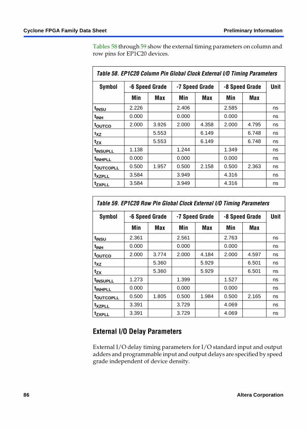
Cyclone FPGA Family Data Sheet Preliminary Information
Tables 58 through 59 show the external timing parameters on column and row pins for EP1C20 devices.
External I/O Delay Parameters
External I/O delay timing parameters for I/O standard input and output adders and programmable input and output delays are specified by speed grade independent of device density.
Table 58. EP1C20 Column Pin Global Clock External I/O Timing Parameters
Symbol -6 Speed Grade -7 Speed Grade -8 Speed Grade Unit
Min Max Min Max Min Max
tINSU 2.226 2.406 2.585 ns
tINH 0.000 0.000 0.000 ns
tOUTCO 2.000 3.926 2.000 4.358 2.000 4.795 ns
tXZ 5.553 6.149 6.748 ns
tZX 5.553 6.149 6.748 ns
tINSUPLL 1.138 1.244 1.349 ns
tINHPLL 0.000 0.000 0.000 ns
tOUTCOPLL 0.500 1.957 0.500 2.158 0.500 2.363 ns
tXZPLL 3.584 3.949 4.316 ns
tZXPLL 3.584 3.949 4.316 ns
Table 59. EP1C20 Row Pin Global Clock External I/O Timing Parameters
Symbol -6 Speed Grade -7 Speed Grade -8 Speed Grade Unit
Min Max Min Max Min Max
tINSU 2.361 2.561 2.763 ns
tINH 0.000 0.000 0.000 ns
tOUTCO 2.000 3.774 2.000 4.184 2.000 4.597 ns
tXZ 5.360 5.929 6.501 ns
tZX 5.360 5.929 6.501 ns
tINSUPLL 1.273 1.399 1.527 ns
tINHPLL 0.000 0.000 0.000 ns
tOUTCOPLL 0.500 1.805 0.500 1.984 0.500 2.165 ns
tXZPLL 3.391 3.729 4.069 ns
tZXPLL 3.391 3.729 4.069 ns
86 Altera Corporation

Preliminary Information Cyclone FPGA Family Data Sheet
Tables 60 through 65 show the adder delays associated with column and row I/O pins for all packages. If an I/O standard is selected other than LVTTL 24 mA with a fast slew rate, add the selected delay to the external tCO and tSU I/O parameters shown in Tables 45 through 48.
Table 60. Cyclone I/O Standard Column Pin Input Delay Adders
I/O Standard -6 Speed Grade -7 Speed Grade -8 Speed Grade Unit
Min Max Min Max Min Max
LVCMOS 0 0 0 ps
3.3-V LVTTL 0 0 0 ps
2.5-V LVTTL 28 30 33 ps
1.8-V LVTTL 214 235 256 ps
1.5-V LVTTL 326 358 391 ps
SSTL-3 class I −221 −244 −266 ps
SSTL-3 class II −221 −244 −266 ps
SSTL-2 class I −264 −291 −317 ps
SSTL-2 class II −264 −291 −317 ps
LVDS −197 −217 −237 ps
Table 61. Cyclone I/O Standard Row Pin Input Delay Adders
I/O Standard -6 Speed Grade -7 Speed Grade -8 Speed Grade Unit
Min Max Min Max Min Max
LVCMOS 0 0 0 ps
3.3-V LVTTL 0 0 0 ps
2.5-V LVTTL 28 30 33 ps
1.8-V LVTTL 214 235 256 ps
1.5-V LVTTL 326 358 391 ps
3.3-V PCI (1) 0 0 0 ps
SSTL-3 class I −221 −244 −266 ps
SSTL-3 class II −221 −244 −266 ps
SSTL-2 class I −264 −291 −317 ps
SSTL-2 class II −264 −291 −317 ps
LVDS −197 −217 −237 ps
Altera Corporation 87

Cyclone FPGA Family Data Sheet Preliminary Information
Table 62. Cyclone I/O Standard Output Delay Adders for Fast Slew Rate on Column Pins
Standard -6 Speed Grade -7 Speed Grade -8 Speed Grade Unit
Min Max Min Max Min Max
LVCMOS 2 mA 1,105 1,216 1,326 ps
4 mA 601 661 721 ps
8 mA 137 151 164 ps
12 mA 0 0 0 ps
3.3-V LVTTL 4 mA 1,105 1,216 1,326 ps
8 mA 740 814 888 ps
12 mA 130 143 156 ps
16 mA 178 196 213 ps
24 mA 0 0 0 ps
2.5-V LVTTL 2 mA 1,504 1,654 1,804 ps
8 mA 307 338 368 ps
12 mA 338 372 405 ps
16 mA 195 214 234 ps
1.8-V LVTTL 2 mA 1,062 1,168 1,274 ps
8 mA 812 893 974 ps
12 mA 812 893 974 ps
1.5-V LVTTL 2 mA 2,556 2,812 3,067 ps
4 mA 1,613 1,774 1,935 ps
8 mA 1,064 1,170 1,276 ps
SSTL-3 class I 616 678 739 ps
SSTL-3 class II 180 198 216 ps
SSTL-2 class I 528 581 633 ps
SSTL-2 class II 233 256 279 ps
LVDS 147 162 176 ps
Table 63. Cyclone I/O Standard Output Delay Adders for Fast Slew Rate on Row Pins (Part 1 of 2)
Standard -6 Speed Grade -7 Speed Grade -8 Speed Grade Unit
Min Max Min Max Min Max
LVCMOS 2 mA 1,105 1,216 1,326 ps
4 mA 601 661 721 ps
8 mA 137 151 164 ps
12 mA 0 0 0 ps
88 Altera Corporation
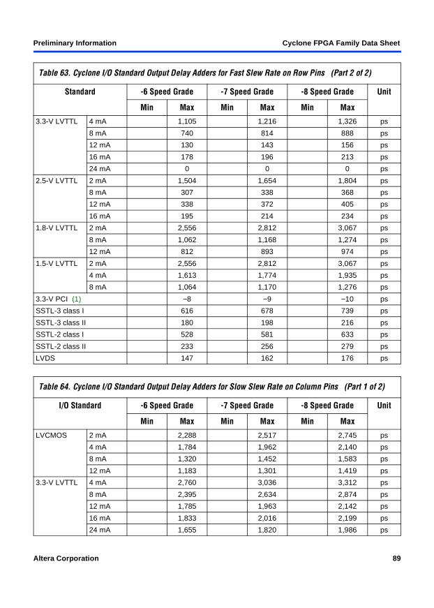
Preliminary Information Cyclone FPGA Family Data Sheet
3.3-V LVTTL 4 mA 1,105 1,216 1,326 ps
8 mA 740 814 888 ps
12 mA 130 143 156 ps
16 mA 178 196 213 ps
24 mA 0 0 0 ps
2.5-V LVTTL 2 mA 1,504 1,654 1,804 ps
8 mA 307 338 368 ps
12 mA 338 372 405 ps
16 mA 195 214 234 ps
1.8-V LVTTL 2 mA 2,556 2,812 3,067 ps
8 mA 1,062 1,168 1,274 ps
12 mA 812 893 974 ps
1.5-V LVTTL 2 mA 2,556 2,812 3,067 ps
4 mA 1,613 1,774 1,935 ps
8 mA 1,064 1,170 1,276 ps
3.3-V PCI (1) −8 −9 −10 ps
SSTL-3 class I 616 678 739 ps
SSTL-3 class II 180 198 216 ps
SSTL-2 class I 528 581 633 ps
SSTL-2 class II 233 256 279 ps
LVDS 147 162 176 ps
Table 64. Cyclone I/O Standard Output Delay Adders for Slow Slew Rate on Column Pins (Part 1 of 2)
I/O Standard -6 Speed Grade -7 Speed Grade -8 Speed Grade Unit
Min Max Min Max Min Max
LVCMOS 2 mA 2,288 2,517 2,745 ps
4 mA 1,784 1,962 2,140 ps
8 mA 1,320 1,452 1,583 ps
12 mA 1,183 1,301 1,419 ps
3.3-V LVTTL 4 mA 2,760 3,036 3,312 ps
8 mA 2,395 2,634 2,874 ps
12 mA 1,785 1,963 2,142 ps
16 mA 1,833 2,016 2,199 ps
24 mA 1,655 1,820 1,986 ps
Table 63. Cyclone I/O Standard Output Delay Adders for Fast Slew Rate on Row Pins (Part 2 of 2)
Standard -6 Speed Grade -7 Speed Grade -8 Speed Grade Unit
Min Max Min Max Min Max
Altera Corporation 89
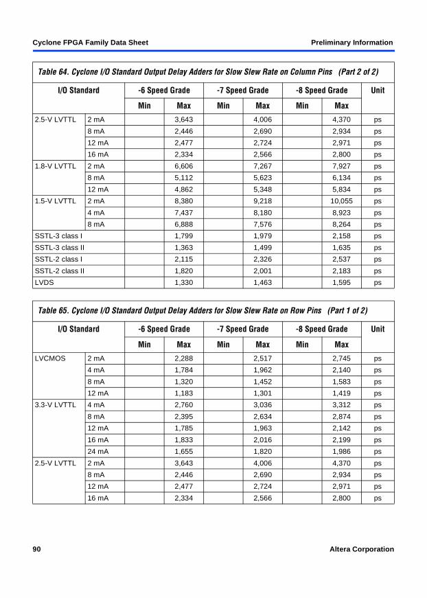
Cyclone FPGA Family Data Sheet Preliminary Information
2.5-V LVTTL 2 mA 3,643 4,006 4,370 ps
8 mA 2,446 2,690 2,934 ps
12 mA 2,477 2,724 2,971 ps
16 mA 2,334 2,566 2,800 ps
1.8-V LVTTL 2 mA 6,606 7,267 7,927 ps
8 mA 5,112 5,623 6,134 ps
12 mA 4,862 5,348 5,834 ps
1.5-V LVTTL 2 mA 8,380 9,218 10,055 ps
4 mA 7,437 8,180 8,923 ps
8 mA 6,888 7,576 8,264 ps
SSTL-3 class I 1,799 1,979 2,158 ps
SSTL-3 class II 1,363 1,499 1,635 ps
SSTL-2 class I 2,115 2,326 2,537 ps
SSTL-2 class II 1,820 2,001 2,183 ps
LVDS 1,330 1,463 1,595 ps
Table 65. Cyclone I/O Standard Output Delay Adders for Slow Slew Rate on Row Pins (Part 1 of 2)
I/O Standard -6 Speed Grade -7 Speed Grade -8 Speed Grade Unit
Min Max Min Max Min Max
LVCMOS 2 mA 2,288 2,517 2,745 ps
4 mA 1,784 1,962 2,140 ps
8 mA 1,320 1,452 1,583 ps
12 mA 1,183 1,301 1,419 ps
3.3-V LVTTL 4 mA 2,760 3,036 3,312 ps
8 mA 2,395 2,634 2,874 ps
12 mA 1,785 1,963 2,142 ps
16 mA 1,833 2,016 2,199 ps
24 mA 1,655 1,820 1,986 ps
2.5-V LVTTL 2 mA 3,643 4,006 4,370 ps
8 mA 2,446 2,690 2,934 ps
12 mA 2,477 2,724 2,971 ps
16 mA 2,334 2,566 2,800 ps
Table 64. Cyclone I/O Standard Output Delay Adders for Slow Slew Rate on Column Pins (Part 2 of 2)
I/O Standard -6 Speed Grade -7 Speed Grade -8 Speed Grade Unit
Min Max Min Max Min Max
90 Altera Corporation

Preliminary Information Cyclone FPGA Family Data Sheet
Note to Tables 60 − 65:(1) EP1C3 devices do not support the PCI I/O standard.
Table 66 shows the adder delays for the IOE programmable delays. These delays are controlled with the Quartus II software options listed in the Parameter column.
1.8-V LVTTL 2 mA 6,606 7,267 7,927 ps
8 mA 5,112 5,623 6,134 ps
12 mA 4,862 5,348 5,834 ps
1.5-V LVTTL 2 mA 8,380 9,218 10,055 ps
4 mA 7,437 8,180 8,923 ps
8 mA 6,888 7,576 8,264 ps
3.3-V PCI 1,175 1,292 1,409 ps
SSTL-3 class I 1,799 1,979 2,158 ps
SSTL-3 class II 1,363 1,499 1,635 ps
SSTL-2 class I 2,115 2,326 2,537 ps
SSTL-2 class II 1,820 2,001 2,183 ps
LVDS 1,330 1,463 1,595 ps
Table 65. Cyclone I/O Standard Output Delay Adders for Slow Slew Rate on Row Pins (Part 2 of 2)
I/O Standard -6 Speed Grade -7 Speed Grade -8 Speed Grade Unit
Min Max Min Max Min Max
Table 66. Cyclone IOE Programmable Delays on Column Pins
Parameter Setting -6 Speed Grade -7 Speed Grade -8 Speed Grade Unit
Min Max Min Max Min Max
Decrease input delay to internal cells
On 3,057 3,362 3,668 ps
Small 2,212 2,433 2,654 ps
Medium 2,639 2,902 3,166 ps
Large 3,057 3,362 3,668 ps
Decrease input delay to input register
On 3,057 3,362 3,668 ps
Increase delay to output pin
On 552 607 662 ps
Altera Corporation 91
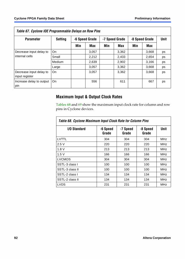
Cyclone FPGA Family Data Sheet Preliminary Information
Maximum Input & Output Clock Rates
Tables 68 and 69 show the maximum input clock rate for column and row pins in Cyclone devices.
Table 67. Cyclone IOE Programmable Delays on Row Pins
Parameter Setting -6 Speed Grade -7 Speed Grade -8 Speed Grade Unit
Min Max Min Max Min Max
Decrease input delay to internal cells
On 3,057 3,362 3,668 ps
Small 2,212 2,433 2,654 ps
Medium 2,639 2,902 3,166 ps
Large 3,057 3,362 3,668 ps
Decrease input delay to input register
On 3,057 3,362 3,668 ps
Increase delay to output pin
On 556 611 667 ps
Table 68. Cyclone Maximum Input Clock Rate for Column Pins
I/O Standard -6 Speed Grade
-7 Speed Grade
-8 Speed Grade
Unit
LVTTL 304 304 304 MHz
2.5 V 220 220 220 MHz
1.8 V 213 213 213 MHz
1.5 V 166 166 166 MHz
LVCMOS 304 304 304 MHz
SSTL-3 class I 100 100 100 MHz
SSTL-3 class II 100 100 100 MHz
SSTL-2 class I 134 134 134 MHz
SSTL-2 class II 134 134 134 MHz
LVDS 231 231 231 MHz
92 Altera Corporation
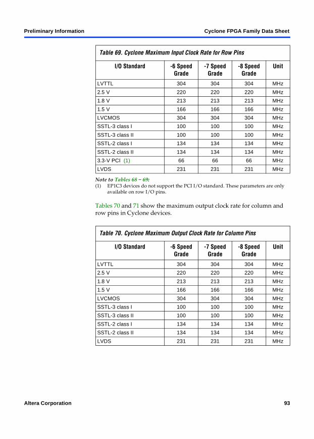
Preliminary Information Cyclone FPGA Family Data Sheet
Note to Tables 68 − 69:(1) EP1C3 devices do not support the PCI I/O standard. These parameters are only
available on row I/O pins.
Tables 70 and 71 show the maximum output clock rate for column and row pins in Cyclone devices.
Table 69. Cyclone Maximum Input Clock Rate for Row Pins
I/O Standard -6 Speed Grade
-7 Speed Grade
-8 Speed Grade
Unit
LVTTL 304 304 304 MHz
2.5 V 220 220 220 MHz
1.8 V 213 213 213 MHz
1.5 V 166 166 166 MHz
LVCMOS 304 304 304 MHz
SSTL-3 class I 100 100 100 MHz
SSTL-3 class II 100 100 100 MHz
SSTL-2 class I 134 134 134 MHz
SSTL-2 class II 134 134 134 MHz
3.3-V PCI (1) 66 66 66 MHz
LVDS 231 231 231 MHz
Table 70. Cyclone Maximum Output Clock Rate for Column Pins
I/O Standard -6 Speed Grade
-7 Speed Grade
-8 Speed Grade
Unit
LVTTL 304 304 304 MHz
2.5 V 220 220 220 MHz
1.8 V 213 213 213 MHz
1.5 V 166 166 166 MHz
LVCMOS 304 304 304 MHz
SSTL-3 class I 100 100 100 MHz
SSTL-3 class II 100 100 100 MHz
SSTL-2 class I 134 134 134 MHz
SSTL-2 class II 134 134 134 MHz
LVDS 231 231 231 MHz
Altera Corporation 93

Cyclone FPGA Family Data Sheet Preliminary Information
Note to Tables 70 − 71:(1) EP1C3 devices do not support the PCI I/O standard. These parameters are only
available on row I/O pins.
Software Cyclone devices are supported by the Altera Quartus II design software, which provides a comprehensive environment for system-on-a-programmable-chip (SOPC) design. The Quartus II software includes HDL and schematic design entry, compilation and logic synthesis, full simulation and advanced timing analysis, SignalTap II logic analysis, and device configuration. See the Design Software Selector Guide for more details on the Quartus II software features.
The Quartus II software supports the Windows 2000/NT/98, Sun Solaris, Linux Red Hat v7.1 and HP-UX operating systems. It also supports seamless integration with industry-leading EDA tools through the NativeLink® interface.
Device Pin-Outs
Device pin-outs for Cyclone devices are available on the Altera web site (http://www.altera.com).
Ordering Information
Figure 39 describes the ordering codes for Cyclone devices. For more information on a specific package, refer to the Altera Device Package Information Data Sheet.
Table 71. Cyclone Maximum Output Clock Rate for Row Pins
I/O Standard -6 Speed Grade
-7 Speed Grade
-8 Speed Grade
Unit
LVTTL 304 304 304 MHz
2.5 V 220 220 220 MHz
1.8 V 213 213 213 MHz
1.5 V 166 166 166 MHz
LVCMOS 304 304 304 MHz
SSTL-3 class I 100 100 100 MHz
SSTL-3 class II 100 100 100 MHz
SSTL-2 class I 134 134 134 MHz
SSTL-2 class II 134 134 134 MHz
3.3-V PCI (1) 66 66 66 MHz
LVDS 231 231 231 MHz
94 Altera Corporation

Preliminary Information Cyclone FPGA Family Data Sheet
Figure 39. Cyclone Device Packaging Ordering Information
Revision History
The information contained in the Cyclone FPGA Family Data Sheet version 1.2 supersedes information published in previous versions.
Version 1.2
The following changes were made to the Cyclone FPGA Family Data Sheet version 1.2: updated the “Power Consumption” section.
Version 1.1
The following changes were made to the Cyclone FPGA Family Data Sheet version 1.1:
Added the EP1C4 device. Updated the “Timing Model” section. Minor textual updates throughout the document.
Device Type
Package Type
6, 7, or 8 , with 6 being the fastest
Number of pins for a particular package
ES:
T:Q:F:
Thin quad flat pack (TQFP)Plastic quad flat pack (PQFP)FineLine BGA
EP1C: Cyclone
3461220
C:I:
Commercial temperature (tJ = 0˚ C to 85˚ C)Industrial temperature (tJ = -40˚ C to 100˚ C)
Optional SuffixFamily Signature
Operating Temperature
Speed Grade
Pin Count
Engineering sample
7EP1C 20 C400F ES
Indicates specific device options or shipment method.
Altera Corporation 95

Cyclone FPGA Family Data Sheet Preliminary Information
Copyright © 2003 Altera Corporation. All rights reserved. Altera, The Programmable Solutions Company, thestylized Altera logo, specific device designations, and all other words and logos that are identified astrademarks and/or service marks are, unless noted otherwise, the trademarks and service marks of AlteraCorporation in the U.S. and other countries. All other product or service names are the property of theirrespective holders. Altera products are protected under numerous U.S. and foreign patents and pendingapplications, maskwork rights, and copyrights. Altera warrants performance of its semiconductor products tocurrent specifications in accordance with Altera’s standard warranty, but reserves theright to make changes to any products and services at any time without notice. Alteraassumes no responsibility or liability arising out of the application or use of anyinformation, product, or service described herein except as expressly agreed to in writingby Altera Corporation. Altera customers are advised to obtain the latest version of devicespecifications before relying on any published information and before placing orders forproducts or services.
®
101 Innovation DriveSan Jose, CA 95134(408) 544-7000http://www.altera.comApplications Hotline:(800) 800-EPLDCustomer Marketing:(408) 544-7104Literature Services:[email protected]
96 Altera Corporation

Preliminary Information Cyclone FPGA Family Data Sheet
Altera Corporation 97