CUTS, COMPUTER USERS TAPE SYSTEM ASSEMBLY and TEST ...
71
CUTS, COMPUTER USERS TAPE SYSTEM ASSEMBLY and TEST INSTRUCTIONS Processor Technology Corporation 6200 Hollis Street Emeryville CA 94608
Transcript of CUTS, COMPUTER USERS TAPE SYSTEM ASSEMBLY and TEST ...

CUTS, COMPUTER USERS TAPE SYSTEM
ASSEMBLY and TEST INSTRUCTIONS
Processor Technology Corporation 6200 Hollis Street Emeryville CA 94608
PROCESSOR TECHNOLOGY CORPORATION
CUTS, COMPUTER USERS TAPE SYSTEM
SECTION
I
II
TITLE
INTRODUCTION and GENERAL INFORMATION
1.1 Introduction • • . • •
1.2 General Information
1.2.1 1.2.2 1.2.3 1.2.4 1.2.5
CUTS Description Receiving Inspection Warranty Information Replacement Parts • Factory Service . . •
ASSEMBLY and TEST
2.1
2.2
2.3
Parts and Components .
Assembly Tips • • •
Assembly Precautions
2.3.1 Handling MOS Integrated 2.3.2 Soldering · · · · · · · 2.3.3 Installing and Removing
Module . · · · · · · ·
Circuits
· · · · CUTS
· · · · · 2.3.4 Installing and Removing Integrated
2.4
2.5
2.6
Circuits · · · · · · · · · · · 2.3.5 Use of Clip Leads · · · · · · · Required Tools, Equipment and Materials
Orientation
Assembly-Test . . . • • • • •
2.6.1 Circuit Board Check •••• 2.6.2 Assembly-Test Procedure ••
III OPTION SELECTION
IV
3.1
3.2
3.3
Option Selection
Port Address Selection (DIP Switch, Sl)
Audio Output Selection •
3.4 Data Rate Selection
OPERATING PROCEDURES
4.1 Tape Recorder
4.2 CUTS-Recorder Interconnect (Single
· ·
· · ·
Recorder) •••••...••••••••
4.3 CUTS-Recorder Interconnect (Two Recorders) ••••.••••••
i
© Processor Technology Corp. 1977
CONTENTS
I-I
I-I
I-I I-I 1-2 1-2 1-2
II-l
II-l
1I-6
1I-6 1I-6
1I-6
1I-6 1I-7
1I-7
1I-7
1I-7
1I-8 1I-9
III-l
III-l
III-l
1II-2
IV-l
IV-l
IV-l

PROCESSOR TECHNOLOGY CORPORATION
CUTS, COMPUrER USERS TAPE SYSTEM
SECTION
IV
V
VI
APPENDICES
TITLE
OPERATING PROCEDURES continued
4.4 Recorder Adjustments .
4.4.1 4.4.2
Volume Control Tone Control
4.5 write Operations .••••
4.6 Read Operations
THEORY OF OPERATION
5.1
5.2
5.'3
Introduction .
Block Diagram Analysis . •••..••
Theory of Operation • • • • . . . • • • •
5.3.1 Timing • • •• . .•. 5.3.2 Control.. • ••••• 5.3.3 write Mode .••••••• 5.3.4 Read Mode .•.•••.•••.••
DRAWINGS
CUTS Assembly Drawing •
CUTS Schematic • • • • • .
I Statement of Warranty
II 8080 Operating Codes
III Standard and Tantalum Dipped Capacitor Color Codes
IV Loading DIP Devices, Soldering Tips and Installing Augat Pins
V IC Pin Configurations
ii
CONTENTS
IV-2
IV-2 IV-2
IV-4
IV-4
V-I
V-I
V-2
V-2 V-4 V-6 V-8
VI-l
VI-2

PROCESSOR TECHNOLOGY CORPORATION
CUTS, COMPUTER USERS TAPE SYSTEM TABLES/ILLUSTRATIONS
TABLE
2-1
5-1
FIGURE
2-1
2-2
2-3
4-1
5-1
TITLE
CUTS Parts List . • • • • • • • •
Strobe Decoder (U23) Truth Table
TITLE
Identification of components
Heat sink and U7 installation .
CUTS-transport interconnect cabling • •
CUTS-recorder interconnect (two recorders)
CUTS simplified block diagram • • • • • • •
iii
PAGE
II-2,3
IV-6
PAGE
II-4,5
II-9
II-18
IV-3
V-3

SECTION I
INTRODUCTION and
GENERAL INFORMATION
CUTS, COMPUTER USERS TAPE SYSTEM
Processor Technology
Processor Technology Corporation 6200 Hollis Street "Emeryville CA 94608

PROCESSOR TECHNOLOGY CORPORATION
CUTS, COMPUTER USERS TAPE SYSTEM SECTION I
1.1 IN'rRODUCTION
This manual supplies the information needed to assemble, test and use the CUTS, Computer Users Tape System. We suggest that you first scan the entire manual before starting assembly. Then, make sure you have all the parts and components listed in the IIParts List ll (Table 2-1) in Section II. When assembling the module, follow the instructions in the order given.
Should you encounter any problem during assembly, calIon us for help if necessary. If your completed module does not work properly, recheck your assembly step by step. Most problems stem from poor soldering, backward installed components, and/or installing the wrong component. Once you are satisfied that the module is correctly assembled, feel free to ask for our help.
1.2 GENERAL INFORMATION
1.2.1 CUTS Description
CUTS, The Computer Users Tape System is a high speed, simple to use audio cassette interface that operates at 300 and 1200 bps data rates under program control. The recording technique used is asynchronously Manchester coded at 1200 or 2400 Hz and is CUTS/Byte/ Kansas City Standard compatible.
Two separate tape transport control outputs and two cornmon audio inputs and outputs are provided to drive one or two recorders. In addition, CUTS has provision for selecting 1) a low level audio output signal for driving the microphone input to an audio recorder, 2) a high level audio output signal for driving the auxiliary input to an audio recorder, and 3) a 5-volt peak-to-peak square save output for driving a digital recorder. A fully automatic gain control operates in the read mode. Unlike other cassette interfaces, CUTS has absolutely no critical adjustments that must be preset or adjusted during operation.
1.2.2
All Processor Technology software is available on CUTS cassettes at lower cost than equivalent paper tapes.
Receiving Inspection
When your kit arrives, examine shipping container for signs of possible damage to the contents during transit. Then inspect the contents for damage. (We suggest you save the shipping materials for use in returning the module to Processor Technology should it become necessary to do so.) If your CUTS kit is damaged, please write us at once describing the condition so that we can take appropriate action.
I-I
PROCESSOR TECHNOLOGY CORPORATION
CUTS, COMPUTER USERS TAPE SYSTEM SECTION I
1.2.3 warranty Information
In brief, parts that fail because of defects in materials or workmanship are replaced at no charge for 3 months for kits, and one year for assembled products, following the date of purchase. Also, products assembled by the buyer are warranted for a period of 3 months after the date of purchase; factory assembled units carry a one year warranty. Refer to Appendix I for the complete "Statement of Warranty".
1.2.4 Replacement Parts
Order replacement parts by component nomenclature (DM8131 IC or lN2222 diode, for example) and/or a complete description (680 ohm, ~ watt, 5% carbon resistor, for example).
1.2.5 Factory Service
In addition to in-warranty service, Processor Technology also provides factory repair service on out-of-warranty products. Before returning the unit to Processor Technology, first obtain our authorization to do so by writing us a letter describing the problem. After you receive our authorization to return the unit, proceed as follows:
1. Write a description of the problem.
2. Pack the unit with the description in a container suitable to the method of shipment.
3. Ship prepaid to Processor Technology Corporation, 6200 Hollis Street, Emeryville, CA 94608.
Your unit will be repaired as soon as possible after receipt and return shipped to you prepaid. (Factory service charges will not exceed $20.00 without prior notification and your approval.)
1-2

SECTION II
ASSEMBLY
CUTS, COMPUTER USERS TAPE SYSTEM
Processor Technology
Processor Technology Corporation 6200 Hollis Street Emeryville CA 94608

PROCESSOR TECHNOLOGY CORPORATION
CUTS, COMPUTER USERS TAPE SYSTEM SECTION II
2.1 PARTS AND COMPONENTS
Check all parts and components against the "Parts List" (Table 2-1 on Page 11-2). If you have difficulty in identifying any parts by sight, refer to Figure 2-1 on Page 11-3.
2.2 ASSEMBLY TIPS
1. Scan Section II in its entirety before you start to assemble your CUTS kit.
2. In assembling your CUTS, you will be following a stepby-step assembly procedure. FOLLOW THE INSTRUCTIONS IN THE ORDER GIVEN.
3. Assembly steps and component installations are preceded by a set of parentheses. Check off each installation and step as you complete them. This will minimize the chances of omitting a step or component.
4. When installing components, make use of the assembly aids that are incorporated on the CUTS PC board and the assembly drawing. (These aids are designed to assist you in correctly installing the components.)
a. The circuit reference (R3, C10 and U7, for example) for each component is silk screened on the PC board near the location of its installation.
b. Both the circuit reference and value or nomenclature (1.5K and 74LS08, for example) for each component are included on the assembly drawing near the location of its installation.
5. To simplify reading resistor values after installation, install resistors so that their color codes read from left-to-right and top-to-bottom as appropriate (board oriented as defined in Paragraph 2.5 on Page 11- .)
6. Unless specified otherwise in the instructions, install components--especially disc capacitors--as close to the board as possible.
7. Should you encounter any problem during assembly, call on us for help if needed.
11-1

PROCESSOR TECHNOLOGY CORPORATION
CUTS, COMPUTER USERS TAPE SYSTEM SECTION II
Table 2-1. CUTS Parts List
INTEGRATED CIRCUITS
1 1458 or 5558 (U6) 1 6011 (U18)
2 4013 (U3 & U4) 1 74LS04 (U24)
1 4019 (U9) 2 74LS08 (U25 & U26)
1 4023 (Ul) 1 74LSI09 (U20)
1 4024 (UI0) 1 74LS132 (U21)
1 4027 (U2) 2 74LS136 (U14 & U15)
1 4030 (U19) 1 74LS155 (U23)
1 4046 (Ull) 1 74LS163 (U12)
1 4049 (U22) 1 74LS175 (U13)
1 4520 (U8 ) 2 74367 (U16 & U17)
REGULATORS TRANSISTORS
1 7805UC or LM340T-5.0. (U7 ) 3 2N2222 (Ql, Q3 & Q4)
1 78L12 (U5) 1 2N2907 (Q5)
1 2N4360 (Q2)
DIODES RELAYS
3 lN4148 (Dl, D2 & D4) 2 DIP Reed, SIGMA 191TEIAl-55 (Kl & K2)
1 IN5242 (D3)
II-2

PROCESSOR TECHNOLOGY CORPORATION
CUTS, COMPUTER USERS TAPE SYSTEM SECTION II
Table 2-1. CUTS Parts List (Continued).
RESISTORS CAPACITORS
1 39 ohm, 2 watt, 5% 1 470 pfd, disc
1 100 ohm, ~ watt, 5% 4 .001 ufd, disc
2 470 ohm, ~ watt, 5% 1 .001 ufd, Mylar tubular
3 1.5K ohm, ~ watt, 5% 1 .01 ufd, Mylar tubular
9 10 K ohm, ~ watt, 5% 19 .1 ufd, disc
4 100 K ohm, ~ watt, 5% 2 1 ufd, tantalum dipped
2 150 K ohm, ~ watt, 5% 3 15 ufd, tantalum dipped
2 1 M ohm, ~ watt, 5%
1 2.2M ohm, ~ watt, 5%
1 50 K ohm Potentiometer
2 2.2K ohm Resistor Network
MISCELLANEOUS
1 CUTS PC Board 10 Molex Crimp Pins for Female
1 Heat Sink Mating Connector
11 14-pin DIP Socket 3 Augat Pin
11 16-pin DIP Socket 1 Length #24 Bare Wire
1 40-pin DIP Socket 1 Length Solder
1 8-position DIP Switch 3 6-32 x J..z Screw
2 Right Angle Molex Connector, 3 #6 Lockwasher
Male (Jl & J2) 3 6-32 Hex Nut
2 Mating Connector for Above, 1 Manual Female (PI & P2)
11-3

PROCESSOR TECHNOLOGY CORPORATION
CUTS, COMPUTER USERS TAPE SYSTEM
TRANSISTOR TO-IS Package (Metal Can)
TRANSISTOR, POWER or REGULATOR IC TO-220 Package
METAL FILM PRECISION RESISTOR (1% Tolerance)
SECTION II
TRANSISTOR TO-92 Package (Plastic)
c
CARBON RESISTOR
5% (gold), 10% (silver.
See Appendix III for Color Code
RESISTOR NETWORK
Figure 2-1. Identification of components.
11-4

PROCESSOR TECHNOLOGY CORPORATION
CUTS, COMPUTER USERS TAPE SYSTEM
ELECTROLYTIC CAPACITOR (Vertical Mount)
DISC CAPACITOR
Monolythic (left) and Ceramic
SECTION II
DIPPED TANTALUM ELECTROLYTIC CAPACITOR
VEI-LOW ~ BRO~N} =~::".:~~ GREeN,
BLUE. . '--~
\5" .t{.+d
See Appendix III for Color Code
MYLAR TUBULAR CAPACITOR
INTEGRATED CIRCUIT, Dual Inline Package (DIP) (6,8,14,16,24 and 40 pin)
?tNl..!
Figure 2-1. Identification of componentso
11-5

PROCESSOR TECHNOLOGY CORPORATION
CUTS, COMPUTER USERS TAPE SYSTEM SECTION II
2.3 ASSEMBLY PRECAUTIONS
2.3.1 Handling MOS Integrated Circuits
Many of the IC's used in the CUTS are MOS devices. They can be damaged by static electricity discharge. Always handle MOS IC's so that gQ discharge will flow through the IC. Also, avoid unnecessary handling and wear cotton--rather than synthetic-~clothing when handling these IC's.
2.3.2 Soldering **IMPORTANT**
1. Use a fine tip, low-wattage iron, 25 watts maximum.
2. DO NOT use excessive amounts of solder. DO solder neatly and as quickly as possible.
3. Use only 60-40 rosin-core solder. NEVER use acid-core solder or externally applied fluxes.
4. To prevent solder bridges, position iron tip so that it does not touch adjacent pins and/or traces simultaneously.
5. DO NOT press tip of iron on pad or trace. To do so can cause the pad or trace to "lift" off the board and permanently damage it.
6. The flow through to solder bridges. component.
CUTS circuit board has plated-through holes. Solder the component (front) side of the board can produce
Check for such bridges after you install each
7. The CUTS circuit board has an integral solder mask (a lacquer coating) that shields selected areas on the board. This mask minimizes the chances of creating solder bridges during assembly. DO, however, check all solder joints for possible bridges.
8. Additional pointers on soldering are provided in Appendix III of this manual.
2.3.3 Installing and Removing CUTS Module
NEVER install the CUTS in, or remove it from the computer with the power on. To do so can damage the module.
2.3.4 Installing and Removing Integrated Circuits.
NEVER install or remove integrated circuits while power is applied to the CUTS. To do so can damage the IC.
11-6

PROCESSOR TECHNOLOGY CORPORATION
CUTS, COMPUTER USERS TAPE SYSTEM SECTION II
2.3.5 Use of Clip Leads
NEVER attach clip leads to the top edge of the CUTS PC board. To do so can short the +8, +16 and -12 V dc buses to one another.
2.4 REQUIRED TOOLS, EQUIPMENT AND MATERIALS
The following tools, equipment and materials are recommended for assembling and testing the CUTS Module:
1. Needle nose pliers
2. Diagonal cutters
3. Scredriver
4. Sharp knife
5. Controlled heat fine tip soldering iron, 25 watts
6. 60-40 rosin-core solder (supplied)
7. #24 bare wire (supplied)
8. Volt-ohm meter
2.5 ORIENTATION
The heat sink area (large foil area) will be located in the upper right-hand corner of the board when the edge connector is at the bottom. In this position, the component (front) side of the board is facing up and the solder (back) side is facing down. In addition. the IC legends (Ul through U4, U8 through U15, etc.) will read from left to right. Subsequent position references in the instructions related to the CUTS PC board assume this orientation.
2.6 ASSEMBLY-TEST
Refer to the assembly drawing in Section VI.
CAUTION
THE CUTS MODULE USES MANY MOS b~D CMOS INTEGRATED CIRCUITS. THEY CAN BE DAMAGED BY STATIC ELECTRICITY DISCHARGE. HANDLE THESE IC's SO THAT NO DISCHARGE FLOWS THROUGH THE IC. AVOID UNNECESSARY HANDLING AND WEAR COTTON--RATHER THAN SYNTHETIC--CLOTHING WHEN YOU DO HANDLE THESE IC's. (STATIC CHARGE PROBLEMS ARE MUCH WORSE IN LOW HUMIDITY CONDITIONS.)
11-7

PROCESSOR TECHNOLOGY CORPORATION
CUTS, COMPUTER USERS TAPE SYSTEM SEC'l'ION II
2.6.1 Circuit Board Check
( t Visually check CUTS PC board for solder bridges (shorts) between traces, broken traces and similar defects.
Check board to insure that the +S-volt line, +16-volt line, +5-volt bus, +12-volt bus and -12-volt bus are not shorted to one another or to ground. Using an ohmmeter, make the following measurements (refer to CUTS assembly drawing in Section VI.):
(~
(~
(~
+S-volt Line Test. Measure between edge connector pin 1 or 51 (left end of connector) and pin 50 or 100 (right end of connector). There should be no continuity.
+16-volt Line Test. Measure between edge connector pin 2 or 52 and pin 50 or 100. There should be no continuity.
S/16 Volt Line Test. Measure between edge connector pin 1 or 51 and pin 2 or 52. There should be no continuity.
+5-volt Bus Test. Measure between the upper mounting pad for D2 (to the left of location K2) and pin 50 or 100 of the edge connector. There should be no continuity.
+12-volt Bus Test. Measure between upper mounting pad for C9 (in upper right corner below CS) and pin 50 or 100 of edge connector. There should be no continuity.
-12-volt Bus Test. Measure between upper mounting pad for CIS (between U16 and U17) and pin 50 or 100 of edge connector. There should be 'no continuity.
5/12/(-12) Volt Bus Test. Measure between upper mounting pad for C2l (lower left corner) and upper pad for C9, between upper pad for C21 and upper mounting pad for CIS, and between upper pad for C9 and upper pad for CIS. You should measure no continuity in any of the three measurements.
If visual inspection reveals any defects, or you measure continuity in any of the preceding tests, return the board to Processor Technology for replacement.
If the board is not defective, go on to next paragraph.
II-S

PROCESSOR TECHNOLOGY CORPORATION
CUTS, COMPUTER USERS TAPE SYSTEM SECTION II
2.6.2 Assembly-Test Procedure
Step 1. Install heat sink. position the large, black heat sink (flat side to board) over the square foil area in the upper right corner. Orient the sink so that the two triangles of mounting holes in the board are under the two triangular cutouts in the sink. Using two 6-32 screws, lockwashers and nuts, attach heat sink to board. Insert the screws from back (solder) side of board. (See Figure 2-2.)
Step 2. Install U7 (7805UC or LM340T-5.0). position u7 over left-hand cutout in heat sink and observe how the leads must be bent to fit the mounting holes. Note that the center lead (3) must be bent downwards at a point approximately 0.2 inches further from the body than the other two leads. Bend the leads so that no contact is made with the heat sink when U7 is flat against the sink and its mounting hole is aligned with the hole in the sink. Fasten U7 to sink using a 6-32 screw, lockwasher and nut. Insert screw from back (solder) side of .board. Solder and trim leads. (Refer to Figure 2-2.)
. Heat
Upper right-hand~ corner of board
@ I
~ J •. ~ ,~. c..--U7
Figure 2-2. Heat sink and u7 installation.
II-9
PROCESSOR TECHNOLOGY CORPORATION
CUTS, COMPUTER USERS TAPE SYSTEM SECTION II
(W{ Step 3. Install male Molex right angle connectors in locations Jl and J2. Position connector with longer pins facing the top of the board, insert leads in mounting holes and -solder.
(v( Step 4. Install diodes Dl, D2 and D4 (lN4148) l respective locations. position Dl and D2 with
band mark (cathode) at the top and position D4
in their their dark with its band
! at the right. Solder and trim leads.
(') step 5. Install diode D3 (lNS242) in its location. Position D3 with its dark band mark ,(cathode) at the right.
(~
(~
Step 6. Install transistors Ql, Q3 and Q4 (2N2222) in their respective locations. position Ql with its emitter lead (closest to tab on can) at the top and its base lead at the left. Position both Q3 and Q4 with their emitter leads at the right and their base leads at the top. Insert leads and push straight down on transistor until it is 3/16" above the surface of the board. Solder and trim leads.
Step 7. Install transistor Q2 (2N4360) in its location. position Q2 with its flat side at the bottom, insert leads and push straight down on transistor until it is 3/16" above the surface of the board. Solder and trim leads.
( ~ Step 8. Install transistor QS (2N2907) in its location. Position QS with its emitter lead (closest to tab on can) at the right and its base lead at the top. Insert leads and push straight down on transistor until it is 3/16" above the surface of the board. Solder and trim leads.
(~ Step 9. Install all resistors in numerical order in the indicated locations. Bend leads to fit distance between mounting holes, insert leads, pull down snug to board, bend leads outward on solder (back) side of board, solder and trim.
LOCATION VALUE (ohms) COLOR CODE
(~ Rl 100 K brown-black-yellow ( , ) R2 10 K brown-black-orange ( ) R3 1.SK brown-green-red ( ) R4 10 K brown-black-orange C RS 1.SK brown-green-red ( R6 1.SK " " " ( R7 10 K brown-black-orange ( R8 150 K brown-green-yellow ( . R9 10 K brown-black-orange
~~ RIO 1 M brown-black-green Rll 10 K brovm -black-orange
Continued on Page II-II.
11-10

PROCESSOR TECHNOLOGY CORPORATION
CUTS, COMPUTER USERS TAPE SYSTEM
Step 9 continued.
LOCATION
~d~ ~i~ ( - R14 ( . R15
R16 R17 R18 R19 R20
( .) R2l
j!m (:,r VRI
VALUE ( ohms)
2.2M 10 K
150 K 10 K
470 100 100 K
K K
10 10
470 39,2 watt
100 K 100 K
1 M 50 K
SECTION II
COLOR -CODE
red-red-green brown-balck-orange brown-green-yellow brown-black-orange yellow-violet brown brown-black-brown brown-black-yellow brown-black-orange
II II II
yellow-violet-brown orange-white-black brown-black-yellow
II II II
brown-black-green Potentiometer
"A Step 10. Install resistor networks RXI and RX2 (2.2K ohms) in their respective locations. Position RXI so that the dot on its package is at the right end. Position RX2 with its dot at the left end.
CAUTION
THESE RESISTOR NETWORKS ARE DELICATE. HANDLE WITH CARE.
( ) Step 11. Install the five tantalum capacitors in the following locations. Take care to observe proper values and the correct orientation.
, LOCATION VALUE (ufd) ORIENTATION
l~ C7 15 11+11 lead left C8 15 11+11 lead top left
~ ·f C21 1 11+11 lead top C24 15 11+11 lead right (t% C29 1 11+11 lead top
( ) Step 12. Install the following capacitors in the indicated locations. Take care to observe the proper value and type for each installation. Bend leads outward on solder (back) side of board, solder and trim.
Continued on Page 11-12.
II-II

PROCESSOR TECHNOLOGY CORPORATION
CUTS, COMPUTER USERS TAPE SYSTEM SECTION II
( JJ) ( ( (
, ( '- (
( ( ) ( Ii )
( ) ( ) ( ( -( ) ( . ) ( ) ( ( ( (' )
(~) ( ) ( . ) ( ) un (If )
(J
Step 12 continued.
Disc capacitor leads are usually coated with wax during the manufacturing process. After inserting leads through mounting holes, remove capacitor and clear the holes of any wax. Re-insert and install.
LOCATION VALUE (ufd)
Cl .1 C2 .1 C3 .1 C4 .01 C5 .1 C6 .1 C9 .1 CIO .1 Cll .001 C12 .1 C13 .1 C14 .001 C15 .1 C16 .1 C17 .1 C18 .1 C19 .1 C20 .001 C22 .001 C23 .1 C25 .001 C26 .1 C27 .1 C28 .1 C30 .1 C31 470 pfd
Disc II
II
Mylar tubular Disc
Mylar tubular Disc
II
II
II
II
Step 13. Install Augat pins in mounting holes A, Band C. (These three holes are located to the left of U16, just below the lower mounting hole for R17.)
NOTE
You will find it helpful to hold the board between two objects so that it stands on edge.
Continued on Page 11-13.
11-12
PROCESSOR TECHNOLOGY CORPORATION
CUTS, COMPUTER USERS TAPE SYSTEM SECTION II
Step 13 continued.
To install an Augat pin, insert it into the mounting hole from the component (front) side of board and solder the pin from the solder (back) side of the board so the solder "wicks up" to the front side. (This will hold the pin firmly in place.)
Then insert a component lead into the pin and reheat the solder. Using the component lead, adjust pin until it is perpendicular to board. Allow solder to cool while holding the pin as steady as possible.
If the cooled solder is mottled or crystallized, a "cold joint" is indicated, and the solder should be reheated.
Step 14. switch so tion, the the first
Install DIP switch in location Sl. Switch No. 1 is at the left. (With ON position of each switch is ~.) seven switches are active.
position this orientaNote that only
(~step 15. Install DIP reed relays in locations Kl and K2. Be sure to position each relay with its end notch at the top (pin 1 in upper left corner). These relays are soldered to
Ihe board. (Refer to "Loading DIP Devices" in Appendix IV.)
(0{ Step 16. Install U6 (1458 or 5558) in its location. PosiU6 with its end notch at the top (pin 1 in upper left corner) and solder to board. (Refer to "Loading DIP Devices" in Appendix IV.)
(~step 17. Install U5 (78L12) in its location just above U6. position u5 with its flat side at the bottom, insert leads and push straight down until it is 3/16" above the surface of the board. Solder and trim leads.
~~tep 18. Install DIP sockets. Install each socket in the indicated location with its end notch oriented as shown on the circuit board and assembly drawing. Take care-not tocreate solder bridges between the pins and/or traces.
INSTALLATION TIP
Insert socket pins into mounting pads of appropriate location. On back (solder) side of board, bend pins at opposite corners of socket (e.g. pins 1 and 9 on a
Continued on Page 11-14.
11-13

PROCESSOR TECHNOLOGY CORPORATION
CUTS, COMPUTER USERS TAPE SYSTEM . SECTION II
Step 18 continued.
l6-pin socket) outward until they are at a 45 0 angle to the board surface. This secures the socket until it is soldered. Repeat this procedure with each socket until all are secured to the board. Solder the unbent pins on all sockets. Then straighten the bent pins to their original position and solder.
LOCATION TYPE SOCKET
Ul 14 pin U2 16 pin U3 14 pin U4 14 pin U8 16 pin U9 16 pin UIO 14 pin Ull 16 pin U12 16 pin U13 16 pin U14 14 pin U15 14 pin U16 16 pin U17 16 pin U18 40 pin U19 14 pin U20 16 pin U2l 14 pin U22 16 pin U23 16 pin U24 14 pin U25 14 pin
( J SteE 19. USin~2:24 bare wire, i::t:~: jumpers according 1 your selection of the options described in Section III.
( ) Step~Q. Set DIP switches (Sl) to select port address as described in Section III.
All Processor Technology software is written with a CUTS port of FA (hex). To set the DIP switches for port FA, place Switch No. 2 in OFF position and the remaining switches in the ON position.
11-14
to

PROCESSOR TECHNOLOGY CORPORATION
CUTS, COMPUTER USERS TAPE SYSTEM SECTION II
(~step 21. Check operation of the regulators. This check is made to prevent potential damage to the IC's from incorrect voltages.
( :../ Using an ohmmeter, make the following measurements:
SUPPLY MEASUREMENT POINTS
+ 5 V dc Ground to right-hand lead of U7 Ground to left-hand lead of U7
+12
-12
V dc Ground to positive (+) lead of C8 Ground to Pin 8 of U6 socket
V dc Across C21
You should measure some resistance in all three measurements. Zero resistance indicates a short. If required, find and correct the problem before proceeding.
J ( ) Install CUTS in computer. (The use of a Processor Tech-nology EXB Extender Board is recommended.)
CAUTION
NEVER INSTALL OR REMOVE CIRCUIT BOARD WITH POWER ON.
Turn power on and make the following voltage measurements:
MEASUREMENT POINTS VOLTAGE (±S%)
Ground to Pin 1 of U18 Socket + 5 V dc
Ground to Pin 8 of U6 Socket +12 V dc
. Ground to Pin 2 of U18 Socket -12 V dc
If any voltage is incorrect, determine and correct the cause before proceeding.
If voltages are correct, turn power off, remove CUTS from computer and go on to Step 22.
Step 22. Install the following IC's in the indicated locations. Pay careful attention to the proper orientation.
Continued on Page II-16.
II-IS

PROCESSOR TECHNOLOGY CORPORATION
CUTS, COMPUTER USERS TAPE SYSTEM SECTION II
( )
Step 22 Continued.
Ste12
Pin 1 is positioned at the upper left corner of each IC location, and is indicated by a dot on the PC board and assembly drawing.
IC NO. TYPE
~~ Ul* 4023* U2* 4027*
( - U3* 4013* ( . U4* 4013* ( U8* 4520* ( u9* 4019* ( . UIO* 4024* ( Ull* 4046* ( U12 74LS163 ( , U13 74LS175 ( U14 74LS136 ( U15 74LS136 ( ) . U16 74LS367 (i U17 74LS367 ( . U18* 6011*
~~) u19* 4030*
!~ U20 74LSI09 U21 74LS132 U2'2* 4049* U23 74LS155
( ) U24 74LS04 .. ~j U25 74LS08 U26 74LS08
*MOS device. Refer to CAUTION on Page II-7.
23. Adjust VRI.
If you do not have a voltmeter, set arrow on VRI to the "10 o'clock" position (as viewed from front side of board when VRI is at the top) and go on to Step 24. (In nearly all cases CUTS operates with VRI at 10 0 I clock. )
Continued on Page II-17
II-16
PROCESSOR TECHNOLOGY CORPORATION
CUTS, COMPUTER USERS TAPE SYSTEM SECTION II
Step 23 continued.
(~ If you selected either the digital or microphon~ audio output options in Step 19, remove the jumper and install a jumper between Augat pins A and B.
(~If you selected the auxiliary option in Step 19, leave tpe jumper between Augat pins A and B installed.
(~onnect pin 2 of Jl (IN) to pin 4 of Jl (OUT).
( Install CUTS in computer and turn power on.
Set VRI fully clockwise (CW). " ,-,,, ) Measure the DC voltage at pin ~of ~ and write the mea
sured voltage down. (Call this Voltage A.)
Set VRI fully counterclockwiseG(CCW). -, t( I,
( Measure the DC voltage at pin ~of JiJ"r and write the measured voltage down. (Call this Voltage B.)
Add Voltages A and B and divide the sum by 2. (Call the result Voltage C.) An example follows:
Voltage A (VRI fully CW): 3.45 V dc
Voltage B (VRI fully CCW): 1.80 V dc
A + B = 5.25 V dc
Voltage C = 5.25 V dc/2 = 2.63 V dc
( ) Adjust VR 1 so that the voltage at pin 3 of U2 equals Voltage C. (In the preceding example this would be 2.63 V dc.)
Step 24. Disconnect pin 2 of Jl from pin 4 of Jl.
() Step 25. If required by your option selection, remove the A-to-B jumper- and re-install the A-to-D or A-to-C jumper as appropriate. Otherwise, leave the A-to-B jumper in and go on to Step 26.
( ) Step 26. Using the two female mating connectors supplied for Jl and J2, fabricate one or two, as required by your needs, CUTS-to-Recorder interconnect cables as shown in Figure 2-3 on Page 11-18.
11-17

PROCESSOR TECHNOLOGY CORPORATION
CUTS, COMPUTER USERS TAPE SYSTEM
Jl PI or J2
or P2
Coaxial Cables (e.g., Audiotex (GC)
Twisted Pair (e.g., Speaker Cable)
30-415-5)
(A)
(A)
(B)
SECTION II
RECORDER CONNECTOR
MONITOR or
EARPHONE
AUXILIARY or
MICROPHONE
REMOTE
1 - Transport 2 - Audio In 3 - Ground
(A) Miniature Phone Plug
(B) Subminiature Phone Plug
4 - Audio Out 5 - Transport Return
Figure 2-3. CUTS-transport interconnect cabling.
11-18

SECTION III
OPTION SELECTION
CUTS, COMPUTER USERS TAPE SYSTEM
Processor Technology
Processor Technology Corporation 6200 Hollis Street Emeryville CA 94608

PROCESSOR TECHNOLOGY CORPORATION
CUTS, COMPUTER USERS TAPE SYSTEM SECTION III
3.1 OPTION SELECTION
Jumper options that control two operating parameters, data rate and audio output, are provided on the CUTS Module. The port address for the module is selectable with seven switches. Use the following selection instructions along with the assembly drawing in Section VI.
3.2 PORT ADDRESS SELECTION (DIP Switch, Sl)
One of 130 possible port addresses, from ¢ through FA (hex), 254 (decimal), for the CUTS is selectable with the first seven DIP switch positions in location Sl.
All Processor Technoloqy software is written for a CUTS port assignment of FA (hex). To configure your CUTS for this port, set Switch No.2 (Sl-2) to OFF and Switch NO's. 1 (Sl-l) and 3 through 7 (Sl-3 through Sl-7) to ON.
To select another port, set Sl-l through Sl-7 as required for the desired address. with these switches the address increases from ¢ (all seven switches open) in a binary fashion to 254, decimal, (all seven switches closed). When setting these switches, keep in m~nd that 1) Sl-7 and Sl-l are the most and least significant bits respectively and 2) a closed switch is equivalent to a binary 1.
3.3 AUDIO OUTPUT SELECTION
The A, B, C, D jumper arrangement (to the left of U16) determines the audio output signal supplied to Jl and J2. Three choices are available: 1) a 5 V peak-to-peak signal for driving digital recorders, 2) a 250 mV signal for driving the auxiliary input to an audio cassette recorder, and 3) a 50 mV signal for driving the microphone input to an audio cassette recorder.
For audio cassette recorders, the auxiliary input is preferred and recommended over the microphone input.
To select the digital recorder output, install a jumper (#24 bare wire is recommended~ between Augat pin A and the mounting pad labeled D.
To select the auxiliary output to drive the auxiliary input (the recommended input) to an audio cassette recorder, install a jumper (#24 bare wire is recommended) between Augat pins A and B.
III-l

PROCESSOR TECHNOLOGY CORPORATION
CUTS, COMPUTER USERS TAPE SYSTEM SECTION III
To select the microphone output to drive the microphone input to an audio cassette recorder, install a jumper (#24 bare wire is recommended) between Augat pins A and C.
3.4 DATA RATE SELECTION
Your CUTS is presently wired for both 1200 and 300 Baud operation, with the selection being program controlled. CUTS is designed, however, for operating at data rates up to 9600 Baud. The pad labeled AA, K, L, Q, R, S, T, U, V, W, X, Y and Z are provided for increasing the data rate. How the board is configured for higher rates will be the subject of a future addendum to this manual.
At this point in time Processor Technology does not recommend operation higher than 1200 Baud.
111-2

SECTION IV
OPERATING PROCEDURES
CUTS, COMPUTER USERS TAPE SYSTEM
Processor Technology
Processor Technology Corporation 6200 Hollis Street Emeryville CA 94608

PROCESSOR TECHNOLOGY CORPORATION
CUTS, COMPUTER USERS TAPE SYSTEM SECTION IV
4.1 TAPE RECORDER
Any standard cassette tape recorder can be used with CUTS providing it has the following features:
useful:
• ALC (automatic level control) in record mode
• II Remote II on-off control input jack
• IIMonitor ll or lIearphone ll output jack
Though not required, the following recorder features will be
• Tone control
e Tape counter
@ IICue ll , IIPause ll or IIInstant Stopll control
Processor Technology currently uses the Panasonic Model RQ-413S with consistently good results.
4.2 CUTS-RECORDER INTERCONNECT (Single Recorder)
Using the interconnect cabling you fabricated in Step 26 of the IIAssembly-Test Procedure ll (Section II), make the following connections: (Refer to Figure 4-1 on Page IV-3. You may use either output connector Jl or J2 on the CUTS.)
1. Plug transport cable (Pins land 5 of Jl or J2) to remote jack on recorder.
2. Connect lIaudio out ll cable (Pin 4 of Jl or J2) to microphone or auxiliary jack on recorder, with the choice depending on the audio output selection you made. (Refer to Paragraph 3.3'in Section III.) The auxiliary input is preferred and recommended over the microphone input.
3. Connect lIaudio inll cable (Pin 2 of Jl or J2) to monitor or earphone jack on recorder.
4.3 CUTS-RECORDER INTERCONNECT (Two Recorders)
Two recorders, under program control, can be driven by CUTS. In this case you will need two sets of the interconnect cabling described in Step 26 of the II Assembly-Test Procedure '\ (Section II).
IV-l
PROCESSOR TECHNOLOGY CORPORATION
CUTS, COMPUTER USERS TAPE SYSTEM· SECTION IV
Using these interconnect cables, connect the CUTS and recorders as shown in Figure 4-1.
When using two recorders you may read or write to both under program control as well as read one tape while writing on the other.
If you intend to read one tape while writing on the other, however, you may have to disconnect the "monitor" plug from the write unit, with the need for disconnect being determined by the recorder design. The monitor disconnect must be made if the recorder provides a "monitor" output in the record mode. (Panasonic RQ-413S and RQ-309DS do, for example.)
4.4
4.4.1
NOTE 1
Recorders on which the "monitor" jack is labeled MONITOR usually provide a monitor output in the record mode. If the jack is labeled EAR or EARPHONE, the recorder usually does not provide a monitor output in the record mode.
NOTE 2
To determine if your recorder provides a monitor output in the record mode, install a blank tape, plug earphone into "monitor" jack and microphone into microphone jack, set recorder controls to record, and speak into microphone while listening with the earphone. If you hear yourself through the earphone, your recorder does provide a monitor output in the record mode.
RECORDER ADJUSTMENTS
Volume Control
Since CUTS cui try in the read the Volume Control write operations.
incorporates AGC (automatic gain control) cirmode and the recorder has ALC in the record mode, setting should not be critical for either read or Simply set the control at midrange and forget it.
4.4.2 Tone Control
If your recorder has a Tone Control, set it at the top (high end) of its range. Tone controls usually have little effect, but it is safer to obtain a fairly high frequency response by setting the control as just described.
IV-2

PROCESSOR TECHNOLOGY CORPORATION
CUTS, COMPUTER USERS TAPE SYSTEM SECTION IV
RECORDER 1
CUTS
Jl PI
1 MC or
2 IN EARPHONE 3 GND I
AUX 4 OUT I REMOTE 5 MC I
MIC
J2 P2
1 MC 1
2 IN 2 MONITOR
GND I or
3 3 EARPHONE
4 OUT I 4 AUX 5 MC I 5 REMOTE
0 MIC
RECORDER 2
Figure 4-1. CUTS-recorder interconnect (two recorders).
IV-3

PROCESSOR TECHNOLOGY CORPORATION
CUTS, COMPUTER USERS TAPE SYSTEM SECTION IV
4.5 WRITE OPERATIONS
Other than placing the recorder in the record mode, loading the tape and making sure that the head is on tape (not leader), no manual operations are needed to write on tape.
4.6 READ OPERATIONS
When reading tapes, you must start the tape at least two seconds ahead of the data block you want to read. (CUTS tapes have a standardized header before each data block.) This two second delay is needed to allow the recorder playback electronics and the CUTS circuitry to stabilize after power is turned on.
Use the following procedure for loading tapes:
1. Disconnect monitor and remote plugs from recorder. (On most recorders this must be done in order to listen to
. the tape.)
2. Load prerecorded cassette and play tape until you hear data. (Data sounds like noise in CUTS format.)
Absence of data is indicated by a pure 1200 Hz or 2400 Hz tone if recorded at 1200 bps or 300 bps respectively in the Byte/Kansas City Standard format.
3. Rewind tape far enough so it will take two seconds to reach the data block you want to read after the recorder is placed in the playback mode. STOP RECORDER AT THIS POINT.
4. Set Volume Control as specified in Paragraph 4.4.1 if necessary.
5. Reconnect monitor and remote plugs to recorder.
6. Place "play" control on recorder in play position.
7. Type in appropriate command on your keyboard. After you strike the RETURN key (in most programs), the recorder will automatically start and data will be read into memory at the locations specified by the CUTS data header or, in the case of BASIC-5 or Processor Technology 8K BASIC, into the proper File or READ statement.
IV-4

SECTION V
THEORY OF OPERATION
CUTS, COMPUTER USERS TAPE SYSTEM
Processor Technology
Processor Technology Corporation 6200 Hollis Street Emeryville CA 94608
PROCESSOR TECHNOLOGY CORPORATION
CUTS, COMPUTER USERS TAPE SYSTEM SECTION V
5.1 INTRODUCTION
The CUTS module functions to transfer data bidirectionally between a computer and one or two audio cassette recorders. To perform its function, the module contains circuitry related to:
1. port address recognition,
2. computer-CUTS buffering,
3. computer input/output command decoding,
4. timing,
5. status reporting,
6. recorder on/Off control,
7. parallel-to-serial and digital-to-audio conversions in the write mode,
8. audio-to-digital and serial-to-parallel conversions in
9. and conversion of read data to NRZ (non-return to zero) format.
5.2 BLOCK DIAGRAM ANALYSIS
A simplified block diagram of the CUTS module is provided in Figure 5-1.
An address selector defines the port address for the CUTS module. It wor¥s with the address decoder to determine if the address on Al-7 matches the port address for the module. If it does, the decoder produces the indicated CARD SELECT output to enable the status in/out and strobe decoders.
Once an input or output request from the processor is recognized, the status in/out decoder enables a PRDY line driver in the wait state generator. This generator inserts one wait state into every input or output request from the processor.
The strobe decoder decodes the indicated inputs from the processor to produce the STATUS WRITE, READ STATUS, DATA READ and DATA WRITE strobe signals.
On an input cycle when A¢ is low, A¢ enables status outputs from the UART, and the strobe decoder outputs a READ STATUS signal. READ STATUS produces a delayed DRIVER ENABLE which gates the UART status to the DI bus. Should A¢ be high, however, the strobe decoder outputs a DATA READ to indicate to the UART that its data has
V-I

PROCESSOR TECHNOLOGY CORPORATION
CUTS, COMPUTER USERS TAPE SYSTEM SECTION V
been accepted. It also resets the driver enable generator to immediately enable the DI bus drivers.
If the cycle is an output cycle and A¢ is high, the strobe decoder outputs a DATA WRITE which transfers DO bus data into the UART and initiates serial transmission by the UART. Should A¢ be low, the strobe decoder outputs a STATUS WRITE. STATUS WRITE strobes the data on D04-7 into the status latch.
The four status bits in this latch are concerned with recorder motor control and data rate. One output turns one recorder motor on and off, another turns a second recorder motor on and off, a third selects a low data rate, and the fourth selects a high data rate.
Timing for the CUTS module is supplied by the clock circuits and read clock. Clock circuitry manipulates ¢2 to supply WRITE CLOCK as well as various other timing signals required to obtain two data rates. Read clock uses NRZ data transitions and one of two clock signals to generate READ CLOCK for use in the read mode.
When CUTS is in the write mode, parallel data on DO¢-7 is serialized in the UART and applied to a synchronizer in the NRZ format. The synchronizer in turn establishes the time at which the bit cell from the UART starts. The digital-to-audio converter converts the data bit levels into corresponding audio signals. These signals are then fed through a driver to the audio output jacks.
In the read mode, inputs from the recorders are mixed and amplified, with an AGC circuit operating on the second stage. Following amplification the audio signals are converted into digital signals, the transitions of which are detected and converted into the NRZ format. NRZ data is applied to the UART which performs the required serial-to-parallel conversion and supplies the parallel data to the DI bus drivers.
5.3 THEORY OF OPERATION
Refer to CUTS schematic in section VI.
5.3.1 Timing
All timing for the CUTS module is derived from, or related to, the 2 MHz ¢2 clock from the computer. As can be seen on the schematic, ¢2 is received on pin 24 of the S-IOO bus by a hysteresis receiver, U21. The inverted ¢2 directly clocks both sections of U20 as well as U12. One half of U20 (clock pin 12) serves as the wait state generator~ the other half generates the DRIVER ENABLE signal.
U12, preset to count 3, divides ¢2 by 13 to produce a 153.85 KHz signal on pin 11. The output of U12 is in turn counted down in
V-2

<: I
W
AI-7
SOUT ----7
SINP ~
¢2 L PSYNC ~
PRDY ~
A¢ PDBIN ---?
PWR --.:;; SOUT ~ SINP~
POC
"-
DO~ -00,0 7
/
( DI¢-7 "-
ADDRESS SELECTOR
(SI)
,~
ADDRESS DECODER (UI4,15)
Ji
STATUS IN/OUT
DECODER (UI4,24)
+ WAIT STATE GENERATOR
(U20)
STROBE DECODER
(U23)
~t STATUS LATCH (UI3)
r> AGC (Q2,3,4)
READ AUDIO/DIGITAL HI-GAIN CLOCK CONVERTER ~ AMP
(US,9,1l) (U6) (U6)
I' ~ ADDRESS SELECT TRANSITION
DETECTOR (UI9,R20,C22)
READ .1 CLOCK
;"~
"'" NRZ DATA
r--' '--I' ..... "- CONVERTER (Ul, 3,4, S) ,
CLOCK ~ ~ ,,~ CIRCUITS ''---I
(Ul,10,12,19) i-J'h. '\
~ 4' ; i.----- DATA WRITE WRITE CLOCK
DATA READ ~
1..----.. READ STATUS
STATUS WRITE 1 -LO 'J' '>. In 'n :, , \11
DRIVER
~ HI "- ENABLE ~
7' GENERATOR UART (U20) (UlS) ,
"
I "
DRIVER ENABLE {}'
BUS DRIVERS (UI6,17)
Figure 5-1. CUTS, simplified block diagram.
I-
~ MIXER-AMP (Ql,R3,4,6)
DRIVER (U22)
l' DIGITAL/AUDI9
CONVERTER "? (U2)
l' ~ SYNCHRONIZER
(U3)
J
MOTOR " CONTROL
--::> (Kl,2)
~ ...
IE---
~
~
~
f----7 IE-r----E--
JI-2
J2-2
JI-4
J2-4
Jl-l JI-5
J2-1 J2-5
() c::: 1-3 Cfl
() 0 :s: 'U
~ I::Ij :;0
c::: Cfl I::Ij ::0 'U Cfl :;0
0 1-3 ()
~ I::Ij 'U Cfl I::Ij Cfl
0 Cfl :;0 t-<: Cfl 1-3 1-3 I::Ij I::Ij ()
:s: ij 0 ~ 0
~ () 0 :;0 'U 0
~ H 0 z:

PROCESSOR TECHNOLOGY CORPORATION
CUTS, COMPUTER USERS TAPE SYSTEM SECTION V
UlO, a seven-stage binary counter, to provide 38.4 KHz on Q2, 19.2 KHz on Q3, 4800 Hz on Q5, 2400 Hz on Q6 and 1200 Hz on Q7. The clocks on Q6 and Q7 are used in the write data synchronizer (U3) and and the digital-to-audio converter (U2).
The remaining outputs from UIO are fed to two sections of U9, a quad multiplexer or select gate. All four sections of U9 are used to select clocks for low speed or high speed operation according to the select inputs, pins 9 (a) and 14 (B). The states of these two select inputs must be complementary to each other in order to select the high or low speed clocks. Specifically, A must be high and B low to select high speed clocks: the converse condition selects low speed clocks. The select inputs are supplied by the complementary outputs of one section in U13, the status latch.
The output of the second section of U9 is WRITE CLOCK, 4800 Hz on low speed and 19.2 KHz on high speed. The third section outputs a 19.2 KHz (high speed) or 38.4 KHz (low speed) timing signal to U8 in the NRZ data conversion circuit.
READ CLOCK is produced by ull (a phase locked loop), U8 (a binary counter) and the remaining two sections in U9. The signal input (pin 14) to ull is supplied from pin 1 of U3 in the NRZ data conversion circuit. It is a constant frequency, regardless of whether one or two transitions are detected in the read data during the count out time (12 counts) of the counter (U8) in the NRZ conversion circuit. A phase comparator in Ull compares the signal input to the output of a voltage controlled oscillator (VCO) in Ull (pin 4). By feeding the VCO output through a counter (the other half of U8) before feeding the counter output back to the compare input (pin 3) of Ull, the circuit acts as a frequency multiplier. The output of this circuit remains locked, therefore, to a multiple of the signal input on pin 14 of Ull.
The output of ull is nominally 19.2 KHz. Remember that the actual output is determined by the signal input which in turn is a function of tape speed. In other words, the phase lock loop circuit tracks input frequency variations. And it will track such variations within its locking range which is determined by the setting of VRI (connected to pin 12 of Ull).
On high speed, the divide by four output of U8 (pin 12) is selected as RECEIVE CLOCK. The VCO output of Ull is selected for the low speed RECEIVE CLOCK.
5.3.2 Control
Basically the wait state generator (~ of U20), address selector and decoder (Sl, u14 and U15), strobe decoder (U23), driver enable generator (~ of U20), the status latch (U13), the status in/ out decoder (U14 and 24), motor control (Kl and 2), and power on clear (U21) comprise the CUTS control circuitry.
V-4
PROCESSOR TECHNOLOGY CORPORATION
CUTS, COMPUTER USERS TAPE SYSTEM SECTION V
The address selector and decoder consists of seven open collector exclusive-OR gates, the inputs of which are connected to Al-~ RXI and Sl. RXI and Sl function as the selector which is configured to reflect the complement of the module address. That is, a response to a high on an address line is generated by the applicable gate by grounding the other input by closing the appropriate DIP switch position. When the decoder senses an address match, all the gates respond true and RX2-4 pulls the outputs up to a high level CARD SELECT signal.
CARD SELECT enables the output gate (U2l) in the status in/ out decoder. This gate is satisfied if, and only if, SOUT or SINP is active to indicate either an input or output operation is under way. The output (pin 6) of U2l enables the PRDY line driver.
The input to this driver is provided on pin 10 of U20, the wait state generator which is clocked by ¢2 and reset by PSYNC. Thus, pin 10 of U20 goes high on the falling edge of ¢2 after PSYNC. This is the time during which the processor tests for wait requests. The purpose of this half of U20, therefore, is to insert one wait state into every input or output request by the processor. This is required to lengthen the data strobes to durations required by the UART.
U23, the strobe decoder, decodes SINP, PDBIN, SOUT, PWR and A¢ to produce STATUS WRITE, READ STATUS, DATA READ STROBE, and DATA WRITE STROBE. The truth table for U23 is provided in Table S-l on Page V-6. All outputs from U23 are low active.
READ STATUS is applied to the J and K inputs to the other half of U20 which is clocked by ¢2. Thus, an active READ STATUS signal produces a DRIVER ENABLE which is delayed from the strobe by one-half a ¢2 cycle. This signal enables the tri-state buffers (U16 and 17) to place data on the DI bus. Note that a DATA READ STROBE resets U20 to immediately enable the DI bus buffers.
The status latch, U13, latches data present on D04-7. (Note that the data on D04 is not used.) Data is loaded into U13 when the strobe decoder outputs a STATUS WRITE STROBE. Four output bits from this latch select data rate and control the tape recorders. A low on pin 14 energizes K2 to turn recorder #1 on~ a high on this pin de-energizes K2 to turn recorder #1 off. The output on pin 11 of U13 does the same thing for Kl which controls "recorder #2. (Dl and D2, which shunt K2 and Kl respectively, prevent damage to the logic circuitry due to inductive kickback.) The remaining two outputs from U13, the complementary outputs associated with DOS, select either low or high speed operation by selecting the appropriate clocks out of U9. Low speed is selected when pins 3 and 2 of U13 are high and low respectively. When the converse relationship exists, high speed is selected.
V-S

PROCESSOR TECHNOLOGY CORPORATION
CUTS, COMPUTER USERS TAPE SYSTEM SECTION V
Table 5-1., Strobe Decoder (U23) Truth Table.
INPUTS ACTIVE
CARD OUTPUT --
A¢* SELECT PDBIN* SINP* PWR* SOUT* (Low)
L H H H - - READ STATUS
H H H H - - DATA READ STROBE
L H - - L H STATUS WRITE STROBE
H H - - L H DATA WRITE STROBE
*Inputs to CUTS module.
The remaining control circuit, POC (power on clear), initializes the CUTS whenever power is applied. When power is applied, POC on S-IOO bus pin 99 goes low. POC is inverted in one section of U21 to clear the logic in the UART (UlS). In addition, the inverted POC is again inverted in one section of U24 to clear the status register, U13. This clear sets both motor control outputs as well as the high speed select bit high.
5.3.3 write Mode
When the CUTS is in the write mode, data is input to the UART (UlS) under control of the DATA WRITE STROBE signal from U23. Upon completion of this strobe, the transmit sequence is initiated within the UART, with the transmission rate being governed by WRITE CLOCK.
The transmission sequence begins with a start bit, a low (data zero) on the UART's TO output. It is followed by eight data bits and two stop bits, with the number of bits being fixed by the connections to pins 34 through 39 of UIS. This data stream is called NRZ data (non-return to zero) because the data never returns to zero until the next bit cell.
NRZ data from UIS is applied to the D input of U3, aD-type flip-flop which is clocked at 1200 Hz. Consequently, the output on pin 13 of U3 follows the input data on pin 9 after the rising edge of the 1200 Hz clock. This output is connected to the reset (pin 12) of U2, so when the data out of the UART is high, the first section in U2 is forced to a reset condition. In this condition the J and K inputs to the second stage of U2 are held high which allows the flipflop to change state on the rising edge of the clock.
V-6

PROCESSOR TECHNOLOGY CORPORATION
CUTS, COMPUTER USERS TAPE SYSTEM SECTION V
The clock for U2 is 2400 Hz in the high speed mode or 4800 Hz in the low speed mode. This clock is derived from the 2400 Hz output of UIO in conjunction with the low speed select signal NAND gate Ul and exclusive-OR gate U19.
In the high speed mode, pins 4 and 5 of Ul are held low, thus holding pin 6 of Ul high. As a result the 2400 Hz signal is inverted in Ul19 to become the clock for U2.
Pins 4 and 5 of Ul are held high, however, in the low speed mode to enable Ul. In this case R19 and C20 provide a delay in the Ul gate. When the 2400 Hz signal on pin 9 of U19 changes state; so does pin 10 of U19. Also, C20 charges through R19 for several hundred nanoseconds, at which point pin 6 of Ul is brought to the opposite polarity. The output from U19 then goes high. A series of positive pulses, with a pulse width approximately equal to the R19, C20 time constant and occuring at every transition of the 2400 Hz signal, appears on pin 10 of U19. This circuit thus operates as a frequency doubler in the low speed mode to provide a 4800 Hz clock for U2.
The 2400 Hz signal from which the U2 clocks are derived also produces the 1200 Hz clock signal for U3 by toggling the flipflop in UIO. As a result the 1200 Hz signal changes state following a propagation delay after the 2400 Hz signal falls.
As previously stated, the second stage of U2 is allowed to change state on the positive going transitions of the U2 clock as long as the data out of the synchronizer is a 11111. The end result is an output on pin 2 of U2 that is one-half the clock frequency (1200 Hz and 2400 Hz in the high and low speed modes respectively).
Assume the data stream out of the UART goes low (110 11 ). On the next rising edge of the 1200 Hz signal, U3 will reset with Q low and Q high. A low reset on pin 12 of U2 enables the first U2 stage to toggle on the next rising edge of the U2 clock which occurs 1/2400 second after the synchronizer output falls. Remember that the U2 clock moves from a lqw to a high shortly before the 1200 Hz signal did. The reset on pin 12 of U2 is thus removed slightly after the U2 clock occurred. with the J and K inputs to the first U2 stage high, its output will change state on each succeeding low to high transition of U2 clock. The second U2 stage in turn can only toggle on the positive going transition of U2 clock when its J and K inputs are high. Since the inputs are high at one-half the clock rate, by virtue of the first U2 stage, the second U2 stage toggles at one-fourth the clock rate.
The two sections of U2, therefore, operate as a frequency divider, dividing the clock by two when the write data is a 11111 and by four when the data is a 110 11 • Thus, in the low speed mode, four cycles of the 1200 Hz represent a 110 11 and eight cycles of 2400 Hz represent a 11111. In the high speed mode, one cycle of
V-7

PROCESSOR TECHNOLOGY CORPORATION
CUTS, COMPUTER USERS TAPE SYSTEM SECTION V
1200 Hz represents a 11111 and one-half cycle of 600 Hz represents a 110 11 •
The output on pin 2 of U2 is applied to one section in U22 which provides sU'fficient current drive for the R15, 16 and 17 divider network. This divider and a jumper arrangement allow selecting one of three outputs to be fed to the audio output jack *Jl-4 and J2-4}. The A-to-D jumper selects a 4-volt peak-to-peak square wave output for a digital recorder~ the A-to-B jumper selects a 270 mv signal for the auxiliary input to an audio recorder~ the A-to-C jumper selects a 50 mv signal for th~ microphone input to an audio recorder.
5.3.4 Read Mode
When CUTS is in ters oh Jl-2 and J2-2. tive mixer (R3,4 and 6) put of which is applied amplifier U6.
the read mode, data from the recorders enThese two inputs are mixed through a resisand fed to Ql, an emitter follower, the outto the negative input (pin 2) of operational
The first section of U6 is a high gain amplifier, with its gain being determined by R9 and RIO. The output from this amplifier is coupled to the input (pin 6) of the following U6 stage and the base of a Darlington pair (Q3 and 4) which provides high current gain.
Current into the base of Q3 causes C29 to discharge. (C29 charges through R25 to 5 V dc.) The voltage on C29 in turn controls· the gate of FET (field effect transistor) Q2. Q2 functions as a variable resistor which can be changed by its gate voltage. Since Q2 is connected between ground and the input network to the first U6 stage, it serves as a variable shunt. A low gate voltage on Q2 decreases the shunt resistance and the input to u6. In a like manner, a high voltage on C29 results in an increased input to U6. Q2, 3 and 4 with their associated circuitry, therefore, serve as an AGC circuit which limits the input to the second U6 stage to approximately a 2 vol.t peak signal.
The second stage of U6 performs the needed audio to digital conversion. Feedback resistor R12, in conjunction with R13, establishes the level on the positive input (pin 5) of U6. This level, be it positive or negative, is the threshold which the negative input (pin 6) must exceed in order for the output of U6 to switch levels, positive to negative and the converse. Since the feedback loop is regenerative, U6 switches at its maximum rate, and u6 switches on each transition of the audio signal input. It is in this manner that U6 performs the audio to digital conversion.
The digital output of U6 is inverted in one section of U22 and applied to pin 2 of U19, an exclusive-OR gate which is connected as a buffer without inversion. If the output of U22 is low, the
V-8

PROCESSOR TECHNOLOGY CORPORATION
CUTS, COMPUTER USERS TAPE SYSTEM SECTION V
output on pin 3 of u19 is also low and the output on pin 11 of u19 is high. The voltage across C22 under this condition is minimal. When the output of U22 goes high, C22 starts to charge through R20 until pin 2 of U19 crosses the threshold of that gate. At this point pin 3 of U19 goes high, and since the two inputs to the second exclusive-OR gate are both high, pin 11 of U19 goes low. C22 now discharges because pins 2 and 3 of U19 are at the same level so that the circuit can repeat the operation on the next high to low transition at pin 4 of U22. R20, C22 and U19 consequently serve as a transition detector that produces a pulse less than one microsecond long for each transition of the output on pin 4 of U22, regardless of the polarity of the transition.
Transition pulses from U19 clock ~ of U3 and ~ of U4, both of which are D-type flip-flops. A transition pulse clocks U3 to set Q high and Q low to enable a binary counter, US. The Q output of U3 is applied to pin 5 of U4 and the circuit remains in this state until one of two things occurs: 1) a second transition pulse arrives before US reaches count 12 or 2) uS reaches count 12.
If a second transition pulse arrives before count 12, the first U4 stage is set and presents a 11111 to pin 9 of U4. - This is clocked by the -reset of U3 as a low to pin 12 of U4.
If a transition pulse does not arrive before count 12, the first U4 stage presents a 110" to pin 9 of U4. On count 12, the C and D outputs of US go high to reset U3 through Ul. As a result the U4 second stage clock goes high, as does pin 12 of U4. The output on pin 12 of U4, in the NRZ format, is inverted by U22 and applied to the receive input of the UART.
The Q output of U3, which occurs at the actual bit rate of the incoming data, is also used by the receive clock circuitry to reconstruct the receive clock from the data signal.
Received data undergoes serial-to-parallel conversion in the UART and placed on the ROl-S data outputs of the UART WHEN ROD (pin 4 of the UART) is low. The received data is then gated through u16 and 17 to the DI bus.
Four status outputs from the UART can also be enabled when SFD (pin 16) is low. These four bits are FE (framing error), OE (overrun error), DR (data ready) and TBRE (transmitter buffer register empty). They are also gated through U16 and 17 to DI3,4,6 and 7 respectively by a delayed READ STATUS signal.
V-9

SEC'I'ION VI
DRAWINGS
CUTS, COMPUTER USERS TAPE SYSTEM
Processor Technology
Processor Technology Corporation 6200 Hollis Street Emeryville CA 94608

COMPONENT Wf~ING
+8 +8-----
m w ..J w:
+
r ..:.
(n=
+"18 -"IS -------
X~Oy---
via EXT CL~
VI1 ~TC
VI2 STSTS
V!3 0lG1
VI4 FROY -----
ViS ----------
VIS -------
VI7 ------------------
X~OY2 ------------
C/C OSS-PS ------
UNPROC -PROC--20-70
SS ----RUN -----
AOO OSS -PROY------
00 OSS - P!NT ------
;rJ 2 CLK - PHOLO ----
;rJ 1 CLI<;'" --25-75
PHLOA --PSYNC ----
PW~IT--PW~ -----
PINTE---POSH~ ------
AS Aa
A4 A1
A3 A2
A15 AS
A12 A7
AS A8
001---A13---35-85
000---A14------
A10 "A '11-------00 4---00 2------
00 S---OO 3------
00 8---00 7-- 40-90
01 2 ----01 4 -------
01 3 ---01 S ------
01 7 ---01,8 ------
SMI 01 1 -------
SOUT---Ol a -- 4S-SS
SINP ---SINTA --,---
SMEI"!--- SWO -----
SHLTA--SSTACK-----
GNO GNO-- 50-100
t
-f>-
ru 'l:J . 0 -" -IU 2 m -i
F"
m
a I+-w +--_ ~ ~I ----..."...'.-.yy~ ---,
1:"
-" o o
< -I -.L

DATA
----- --=------=----~~=-=-------------~==-------------~
VI-2
JI AUDIO IN
JZ AUDIO IN
F'''' (0 Z 1---_""I.SI\Kr---,/
"'" 10K
JI TAP~ T~AN.sP"'~'Tl
, 31 ~AP" TI<'AN:50I"'OI<Tl Re:TU~N
Jt. TAP. TII'AN"POF<T;z. I
Cit. ZN4~"'O
JZ TAPE TI<'AN~F"OF<T;z. R:&:TUI<'N ~~---------------~
,:~ tJ~ A PL-L- P'1"1P'a!C'/~"UNTi.1I: ~i50U8 '-"'''" ~""
~4;;'.zO 15
® 1
L-----------------------------~'Zz (~~~y)
NOHS:
I. -D I" I/O "'ONN~'::~"I<
1.. ----CJ I~ s.- Ie''' G't'NNi£':::1'IO,,",
~. D-- ," $-100 ""NNI!'::TION
DJ: ¢
.... I~V
-I~V
SCHE:MATIC:,5-IOO CUTS 1----
DRAWN n I,.I"'D ~ MA~~U .-, .... .::.'-8-77 DAn, q-:z.1-7~(,~L_~...:. __ ...:"_~_n ____ .....l_ •• ___ ~ _ _'_
PROC:5SS0R TSCHNOl-06:Y
f':ev. es
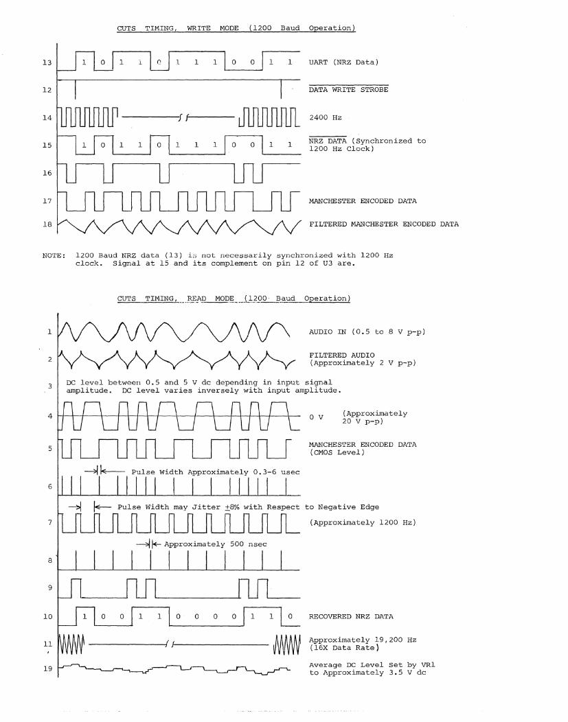
CUTS TIMING, WRITE MODE (1200 Baud Operation)
13 1 1 GJ 1 1 1 0 0 1 1 UART (NRZ Data)
12 DATA WRITE STROBE
14 f ' ) J1J1JWUl 2400 Hz
1 1 1 1 NRZ DATA (Synchronized to 1200 Hz Clock) 15
16
17 MANCHESTER ENCODED DATA
18 FILTERED MANCHESTER ENCODED DATA
NOTE: 1200 Baud NRZ data (13) is not necessarily synchronized with 1200 Hz clock. Signal at 15 and its complement on pin 12 of U3 are.
1
2
3
4
5
6
7
8
9
10
11
19
CUTS
AUDIO IN (0.5 to 8 V p-p)
FILTERED AUDIO (Approximately 2 V p-p)
DC level between 0.5 and 5 V dc depending in input signal amplitude. DC level varies inversely with input amplitude.
-."j I+- Approximately 500 nsec
----------------~f 'r'---------------------~
o V (Approximately 20 V p-p)
MANCHESTER ENCODED DATA (CMOS Level)
to Negative Edge
(Approximately 1200 Hz)
RECOVERED NRZ DATA
Approximately 19,200 Hz (16X Data Rate)
Average DC Level set by VRI to Approximately 3.5 V dc

APPENDICES
I Statement of Warranty
II 8080 Operating Codes
III Standard Color Code
IV Loading DIP Devices, Soldering Tips and Installing Augat Pins
V IC Pin Configurations
Processor Technology
Processor Technology Corporation 6200 Hollis Street Emeryville CA 94608

PROCESSOR TECHNOLOGY CORPORATION
CUTS, COMPUTER USERS TAPE SYSTEM APPENDIX I
PROCESSOR TECHNOLOGY CORPORATION, in recognition of its responsibility to provide quality components and adequate instruction for their proper assembly, warrants its products as follows:
All components sold by Processor Technology Corporation are purchased through normal factory distribution and any part which fails because of defects in workmanship or material will be replaced at no charge for a period of 3 months for kits, and one year for assembled modules, following the date of purchase. The defective part must be returned postpaid to Processor Technology Corporation within the warranty period.
Any malfunctioning module, purchased as a kit directly from Processor Technology and returned to the factory within the three-month warranty period, which in the judgement of PTC has been assembled with care and not subjected to electrical or mechanical abuse, will be restored to proper operating condition and returned, regardless of cause of malfunction, without charge. Kits purchased from authorized PTC dealers should be returned to the selling dealer for the same warranty service.
Any modules purchased as a kit and returned to PTC, which in the judgement of PTC are not covered by the above conditions, will be repaired and returned at a cost commensurate with the work required. In any case, this charge will not exceed $20.00 without prior notification and approval of the owner.
Any modules, purchased as assembled units are guaranteed to meet specifications in effect at the time of manufacture for a period of at least one year following purchase. These modules are additionally guaranteed against defects in materials or workmanship for the same one year period. All warranted factory assembled units returned to PTCO postpaid will be repaired and returned without charge.
This warranty is made in lieu of all other warranties expressed or implied and is limited in any case to the repair or replacement of the module involved.
AI-l

00 NOP 28 50 MOV D.B 01 LXI B.D16 29 DAD H 51 MOV D.C 02 STAX B 2A LHLD Adr 52 MOV 0.0 03 INX B 2B DCX H 53 MOV D.E 04 INR B 2C INR L 54 MOV D.H 05 OCR B 2D DCR L 55 MOV D.L 06 MVI B.D8 2E MVI L.D8 56 MOV D.M 07 RLC 2F CMA 57 MOV D.A 08 30 58 MOV E.B 09 DAD B 31 LXI SP.D16 59 MOV E.C OA LDAX B 32 STA Adr 5A MOV E.D OB OCX B 33 INX SP 5B MOV E.E OC INR C 34 INR M 5C MOV E.H 00 OCR C 35 DCR M 50 MOV E.L OE MVI C.08 36 MVI M.08 5E MOV E.M OF RRC 37 STC 51- MOV E.A 10 38 60 MOV H.B 11 LXI 0.016 39 DAD SP 61 MOV H.C 12 STAX D 3A LOA Adr 62 MOV H.D 13 INX 0 3B DCX SP 63 MOV H.E 14 INR 0 3C INR A 64 MOV H.H 15 OCR 0 3D DCR A 65 MOV H.L 16 MVI 0.08 3E M'II A.DB 66 MOV H.M 17 RAL 3F CMC 67 MOV H.A 18 40 MOV B.B 68 MOV L,B 19 DAD D 41 MOV B,C 69 MOV L.C 1A LOAX 0 42 MOV B.O 6A MOV L.D 1B DCX D 43 MOV B.E 6B MOV L.E 1C INR E 44 MOV B,H 6C MOV L.H lD OCR E 45 MOV B.L 6D MOV L,L 1E MVI E:D8 46 MOV 8,M 6E MOV L,M IF RAR 47 MOV B.A 6F MO'J L,A 20 48 MOV C.B 70 MOV M.B 21 LXI H.DI6 49 MOV C,G 71 MOV M.C 22 SHLD Adr 4A MOV C,D 72 MOV M.D 23 INX H 4B MOV C.E 73 MOV M.E 24 INR H 4C MOV C,H 74 MOV M.H 25 OCR H 4D MOV C.L 75 MOV M,L 26 MVI H.D8 4E MOV C,M 76 HLT 27 DAA 4F MOV C,A 77 MOV M,A
08 = constant, or logical/arithmetic expression that evaluates to an B bit data quantity.
~ H H I I-'
78 MOV A.B AD ANA B C8 RZ 79 MOV A.C Al ANA C C9 RET 7A MOV A.D A2 ANA 0 CA JZ 7B MOV A.E A3 ANA E CB 7C MOV A,H A4 ANA H CC CZ 70 MOV A,L AS ANA L CD CALL 7E MOV A.M A6 ANA M CE ACI 7F MOV A.A A7 ANA A CF RST 1 80 ADD B A8 XRA B DO RNC 81 ADD C A9 XRA C Dl POP D 82 ADD D AA XRA D D2 JNC 83 ADD E AB XRA E D3 OUT 84 ADD H AC XRA H 04 .CNC 85 ADD L AD XRA L 05 PUSH 0 86 ADD M AE XRA M D6 SUI 87 ADD A AF XRA A D7 RST 2 88 ADC S BO ORA B 08 RC 89 ADC C Bl ORA C 09 8A ADC D B2 ORA 0 DA JC 8B AOC E B3 ORA E DB IN BC AOC H B4 ORA H DC CC 80 ADC L B5 ORA L DO BE ADC M B6 ORA M DE SBI 8F ADC A B7 ORA A DF RST 3 90 SUB B B8 CMP B EO RPO 91 SUB C B9 CMP C El POP H 92 SUB D BA CMP D E2 JPO 93 SUB E BB CMP E E3 XTHL 94 SUB H BC CMP H E4 CPO 95 SUB L BD CMP L E5 PUSH H 96 SUB M BE CMP M E6 ANI 97 SUB A BF CMP A E7 RST 4 98 SBB B CO RNZ E8 RPE 99 SBB C Cl POP B E9 PCHL 9A SBB 0 C2 JNZ Adr EA JPE 9B SBB E C3 JMP Adr E8 XCHG 9C S88 H C4 CNZ Adr EC CPE 9D SB8 L C5 PUSH B ED 9E SB8 M C6 ADI D8 EE XRI 9F SBB A C7 RST 0 EF RST 5
016 = constant, or logical/arithmetic expression that evaluates to a 16 bit data quantity.
Processor Technology
Processor Technology Corporation 6200 Hollis Street .Emeryville CA 94608
FO RP F1 POP PSW F2 JP Adr F3 01
Adr F4 CP Adr Adr F5 PUSH PSW D8 F6 ORI 08
F7 RST 6 F8 RM F9 SPHL
Adr FA JM Adr D8 FB EI Adr FC CM Adr
FO 08 FE CPI 08
FF RST 7
Adr D8 Adr
D8 HEX-ASCII TABLE
Non-Printing
Adr 00 NULL 07 BELL
Adr 09 TAB OA LF
D8 OB VT OC FORM OD CR 11 X-ON
Adr 12 TAPE 13 X-OFF
Adr 14 lB ESC
08 7D ALT MODE 7F RUB OUT
Adr = 16 bit address
HEX-ASCII TABLE
Printing 30 0 31 1 32 2 33 3 34 4 35 5 36 6 37 7 38 8 39 9
41 A 42 B 43 C 44 0 45 E 46 F 47 G 48 H 49 I 4A J 4B K 4C L 4D M 4E N 4F 0 50 P 51 Q 52 R 53 S 54 T 55 U 56 V 57 W 58 X 59 Y SA Z
Characters 40 20 21 22 23 24 25 26 27 28 29 2A 2B 2C 2D 2E 2F 3A 3B 3C 3D 3E 3F 5B 5G 5D 5E 5F
@ space
# $ ~/o
&
+
<
:->
?
(,\) (-)
» "'C "'C m Z o X
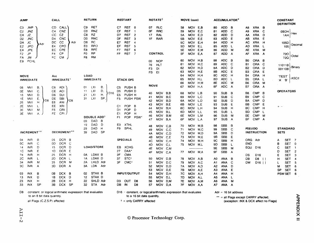
JUMP CALL RETURN RESTART ROTATE+ MOVE (conti ACCUMULATOR* CONSTANT DEFINITION
C3 JMP CO CALL C9 RET C7 RST 0 07 ALC 58 MOV E,B 80 ADD B A8 XRA B C2 JNZ C4 CNZ CO RNZ CF RST 1 OF RAC 59 MOV E,C 81 ADD C A9 XRA C OBDHf CA JZ CC CZ C8 RZ 07 RST 2 17 RAL 5A MOV E,O 82 ADD 0 AA XRA 0 lAH Hex 02 .JNC 04 CNC DO RNC OF RST 3 IF RAR 5B MOV E,E 83 ADD E AB XRA E DA JC Adr DC CC Adr 08 RC E7 RST 4 5C MOV E,H 84 ADD H AC XRA H 1050 f . E2 JPO E4 CPO EO RPO EF RST 5 50 MOV E,L 85 ADD L AD XRA L 105 Decimal EA JPE EC CPE E8 RPE F7 RST 6 5E MOV E.M 86 ADD M AE XRA M F2 JP F4 CP FO RP FF AST 7 CONTROL 5F MOV E,A 87 ADD A AF XRA A 720f FA JM FC CM F8 RM 720 Octal E9 PCHL 00 NOP 60 MOV H,B 88 AOC B BO ORA B
76 HLT 61 MOV H,C 89 AOC C Bl ORA C 11011B} . F3 01 62 MOV H,O 8A AOC 0 B2 ORA 0 00110B Binary FB EI 63 MOV H,E 8B AOC E B3 ORA E
MOVE Ace LOAD 64 MOV H,H 8C AOC H B4 ORA H 'TEST' } IMMEDIATE IMMEDIATE* IMMEDIATE STACK OPS 65 MOV H,L 80 AOC L B5 ORA L 'A' 'B' ASCII
66 MOV H.M 8E AOC M B6 ORA M 06 MVI S. C6 AOI 01 LXI
B I C5 PUSH B MOVE 67 MOV H.A 8F AOC A B7 ORA A OE MVI C. CE ACI 11 LXI ~: 016
05 PUSH 0 MOV SUB CMP OPERATORS 16 MVI O. 06 SUI 21 LXI E5 PUSH H 40 MOV B,B 68 L,B 90 B B8 B
1E MVI E. DE SBI 31 LXI SP. F5 PUSH PSW 41 MOV B,C 69 MOV L.C 91 SUB C B9 CMP C
26 MVI H 08 E6 ANI 08 42 MOV B,O 6A MOV L.D 92 SUB 0 BA CMP 0
2E MVI L. EE XAI Cl POP B 43 MOV B,E 6B MOV L.E 93 SUB E BB CMP E MOV B.H 6C MOV L,H 94 SUB H BC CMP H + -
36 MVI M. F6 ORI 01 POP 0 44
3E MVI A. FE CPI E1 POP H 45 MOV B.L 60 MOV L,L 95 SUB L BO CMP L DOUBLE ADD+ Fl POP PSW· 46 MOV B.M 6E MOV L.M 96 SUB M BE CMP M
09 DAD B 47 MOV B,A 6F MOV L,A 97 SUB A BF CMP A
19 DAD 0 E3 XTHL 48 MOV C.B 70 MOV M,B 98 SBB B 29 DAD H F9 SPHL 49 MOV C,C 71 MOV M,C 99 SBB C PSEUDO STANDARD
INCREMENT** DECREMENT"'''' 39 DAD SP 4A MOV C.O 72 MOV M,O 9A SBB 0 INSTRUCTION SETS 4B MOV C,E 73 MOV M.E 9B SBB E
04 INR S 05 OCR B SPECIALS 4C MOV C,H 74 MOV M,H 9C SBB H ORG Adr A SET 7 OC INR C 00 OCR C 40 MOV C,L 75 MOV M.L 90 SSB L END B SET 0 14 INR 0 15 OCR 0 LOAD/STORE EB XCHG 4E MOV C,M ._------------ 9E SBB M EOU 016 C SET 1 1C INR E 10 OCR E 27 DAA' 4F MOV C.A 77 MOV M,A 9F SSB A 0 SET 2 ?4 INR H 25 OCR H OA LDAX B 2F CMA OS 016 E SET 3 2C INR L 20 OCR L 1A LDAX 0 37 STCt 50 MOV D.B 78 MOV A.B AO ANA B DB 08 ( I H SET 4 34 INR M 35 OCR M 2A LHLD Adr 3F CMC+ 51 MOV D,C 79 MOV A,C Al ANA C OW 016 " L SET 5 3C iNR A 3D OCR A 3A LOA Adr 52 MOV 0,0 7A MOV A,O A2 ANA 0 M SET 6
53 MOV D,E 7B MOV A,E A3 ANA E SP SET 6 03 INX B DB OCX B 02 STAX B INPUT/OUTPUT 54 MOV O.H 7C MOV A,H A4 ANA H PSWSET 6 13 INX 0 1B OCX 0 12 STAX 0 55 MOV O,L 70 MOV A,L A5 ANA L 23 INX H 2B DCX H 22 SHLD Adr 03 OUT 08 56 MOV D,M 7E MOV A,M A6 ANA M 33 INX SP 3B DCX SP 32 STA Adr DB IN 08 57 MOV D,A 7F MOV A,A A7 ANA A
08 constant, or logicaL-arithmetic expression that evaluates 016 - constant, or 10gicaVarithmetic expression that evaluates Adr ~ 16 bit address to an 8 bit data quantity. to a 16 bit data quantity. •• ~ all Flags except CARRY affected; »
"0 all Flags (C.Z.S.P) affected t = only CARRY affected (exception: INX & DCX affect no Flags) "0
m :2
~ 0 H X H I © Processor Technology Corp.
I\)

PROCESSOR TECHNOLOGY CORPORATION
CUTS, COMPUTER USERS TAPE SYSTEM APPENDIX III
The electrical value of many types of resistors and capacitors is printed on the component. Other types, however, are identified by color coding which gives all the information needed to correctly identify the component. In most cases color coding conforms with the EIA (Electronic Industries Association) Standard Color Code. In other cases a manufacturer will adapt the standard to fit his particular requirement. Both the Standard 'ColorCode and a code used to identify tantalum dipped capacitors are provided below.
STANDARD COLOR CODE FOR RESISTORS AND CAPACITORS
SIGNIFICANT DECIMAL COLOR FIGURE MULTIPLIER
Black 0 1 Brown 1 10 Red 2 100 Orange 3 1,000 Yellow 4 10,000 Green 5 100,000 Blue 6 1,000,000 Violet 7 10,000,000 Gray 8 100,000,000 White 9 1,000,000,000 Gold - 0.1 Silver - 0.01 None - ---*Applies to capacitors only.
COLOR CODE FOR TANTALUM DIPPED CAPACITORS
Rated CODE FOR CAPACITANCE Voltage Color IN PICOFARADS
VDC 25°C 1st 2nd Multiplier Fiqure Fiqure uuF
3-4 Black 0 0 1 3-6 Brown 1 1 10 3-10 Red 2 2
./
100 3-15 Orange 3 3 1,000 3-20 Yellow 4 4 10,000 3-25 Green 5 5 100,000 3-35 Blue 6 6 1,000,000 3-50 Violet 7 7 10,000,000
Gray 8 8 3 White 9 9
AIII-l
TOLERANCE VOLTAGE (%) RATING*
--100 200 300 400 500 600 700 800 900
5 1000 10 2000 20 500
[Polarity & Voltage
1st Figure ~ 2nd Figure
~-Mul tiplier
+

PROCESSOR TECHNOLOGY CORPORATION
CUTS, COMPUTER USERS TAPE SYSTEM APPENDIX IV
LOADING DIP (DUAL IN-LINE PACKAGE) DEVICES
Most DIP devices have their leads spread so that they can not be dropped straight into the board. They must be "walked in" using the following procedure:
(1) Orient the device properly. Pin 1 is indicated by a small embossed dot on the top surface of the device at one corner. Pins are numbered counterclockwise from pin 1.
(2) Insert the pins on one side of the device into their holes on the printed circuit card. Do not press the pins all the way in, but stop when they are just starting to emerge from the opposite side of the card.
(3) Exert a sideways pressure on the pin~ at the other side of the device by pressing against them where they are still wide below the bend. Bring this row of pins into alignment with its holes in the printed circuit card and insert them an equal distance, until they begin to emerge.
(4) Press the device straight down until it seats on the points where the pins widen.
(5) Turn the card over and select two pins at opposite corners of the device. Using a fingernail or a pair of long-nose pliers, push these pins outwards until they are bent at a 45 0
angle to the surface of the card. This will secure the device until it is soldered.
SOLDERING TIPS
(1) Use a low-wattage iron--25 watts is good. Larger irons run the risk of burning the printed-circuit board. DonUt try to use a soldering gun, they are too hot.
(2) Use a small pointed tip and keep it clean. Keep a damp piece of sponge by the iron and wipe the tip on it after each use.
(3) Use 60-40 rosin-core solder ONLY. der or externally applied fluxes. solder you can get.
DO NOT use acid-core solUse the smallest diameter
NOTE: DO NOT press the top of the iron on the pad or trace. This will cause the trace to "lift" off of the board which will result in permanent damage.
(4) In soldering, wipe the tip, apply a light coating of new solder to it, and apply the tip to both parts of the joint, that is, both the component lead and the printed-circuit pad. Apply the solder against the lead and pad being heated, but not directly to the tip of the iron. Thus, when the solder
AIV-l

PROCESSOR TECHNOLOGY CORPORATION
CUTS, COMPUTER USERS TAPE SYSTEM APPENDIX IV
melts the rest of the joint will be hot enough for the solder to "take", (i.e., form a capillary film).
(5) Apply solder for a second or two, then remove the solder and keep the iron tip on the joint. The rosin will bubble out. Allow about three or four bubbles, but don't keep the tip applied for more than ten seconds.
(6) Solder should follow the contours of the original joint. A blob or lump may well be a solder bridge, where enough solder has been built upon one conductor to overflow and "take" on the adjacent conductor. Due to capillary action, these solder bridges look very neat, but they are a constant source of trouble when boards of a high trace density are being soldered. Inspect each integrated circuit and component after soldering for bridges.
(7) To remove solder bridges, it is best to use a vacuum "solder puller" if one is available. If not, the bridge can be reheated with the iron and the excess solder "pulled" with the tip along the printed circuit traces until the lump of solder becomes thin enough to break the bridge. Braid-type solder remover, which causes the solder to "wick up" away from the joint when applied to melted solder, may also be used.
INSTALLING AUGAT PINS
Augat pins are normally supplied on carriers (e.g., 8-pin and 16-pin carriers). In many cases the PC board layout permits Augat pins to be installed while still attached to the carrier or a portion of the carrier. In other cases the pins must be installed singly.
To install two or more pins that are still attached to the carrier, proceed as follows:
It is perfectly alright to appropriately cut a carrier to accommodate the installation. For example, an 8-pin carrier can be cut in half (4 pins each) across the short dimension to fit a 4-pin, 4-corner layout. It may also be cut in half along the long dimension to fit a 4-pin, inline layout.
(1) Insert pins in the mounting holes from the front (component) side of board. (The carrier will hold the pins perpendicular to the board.)
(2) Solder all pins from back (solder) side of board so the solder "wicks up" to the front side.
AIV-2

PROCESSOR TECHNOLOGY CORPORATION
CUTS, COMPUTER USERS TAPE SYSTEM APPENDIX III
(3) Check for solder bridges.
(4) Remove carrier.
To install single pins, proceed as follows:
(1) Hold board between two objects so that it stands on edge.
(2) Insert pins in the mounting holes from front (component) side of board.
(3) Solder pins from back (solder) side of board so the solder "wicks Up" to the front side. (This will hold the pins firmly in place.)
(4) Insert a component lead into one pin and reheat the solder. Using the component lead, adjust pin until it is perpendicular to board. Allow solder to cool while holding the pin as steady as possible. Remove component lead. Repeat this procedure with other pins.
If cooled solder is mottled or crystallized, a "cold joint" is indicated, and the solder should be reheated.
(5) Check each installation for cold joints and solder bridges.
AIV-3

PROCESSOR TECHNOLOGY CORPORATION
CUTS, COMPUTER USERS TAPE SYSTEM
1458 or 5558
!l"".",,;. ".,,;, " L I
""-",,'
''',''','',,'
4019
4024 VDD Ne nl Q2 Ne QJ Ne
I .. 1l 12 11 10 9 •
r-- l-
I 2 1 • S 6 I' INPUT RESET n, n6 ns n.
PULSES
4030
VDO
" I~l--+-'-'----l' 1,"-----J!--~I-·-L.Lr t~r-td_____ _ ___ C)
Q--- '-rQ I r,-l . + ;------1' I'
v _
4013
4023
4027
4046
AV-1
APPENDIX V
n, a, '.
'.
Voo QI 0.1 CLOCK 1 RESET 1 XI Jl SET 1
p--D2 Q2 ClO(l\l R'-SI r 1 10
16 -'''''00
I~ - z!.,,;.~,
vc;:, OuT -- Jj rOf 13
IM1:~' r - :. VIEW 12
10
~",.i. C':'" n Q<.:r
R.i: 11) "ss
Ii: 11J v~';.
C>£",""-.:," ,,-., VSS- 8 Yeu IN
I'
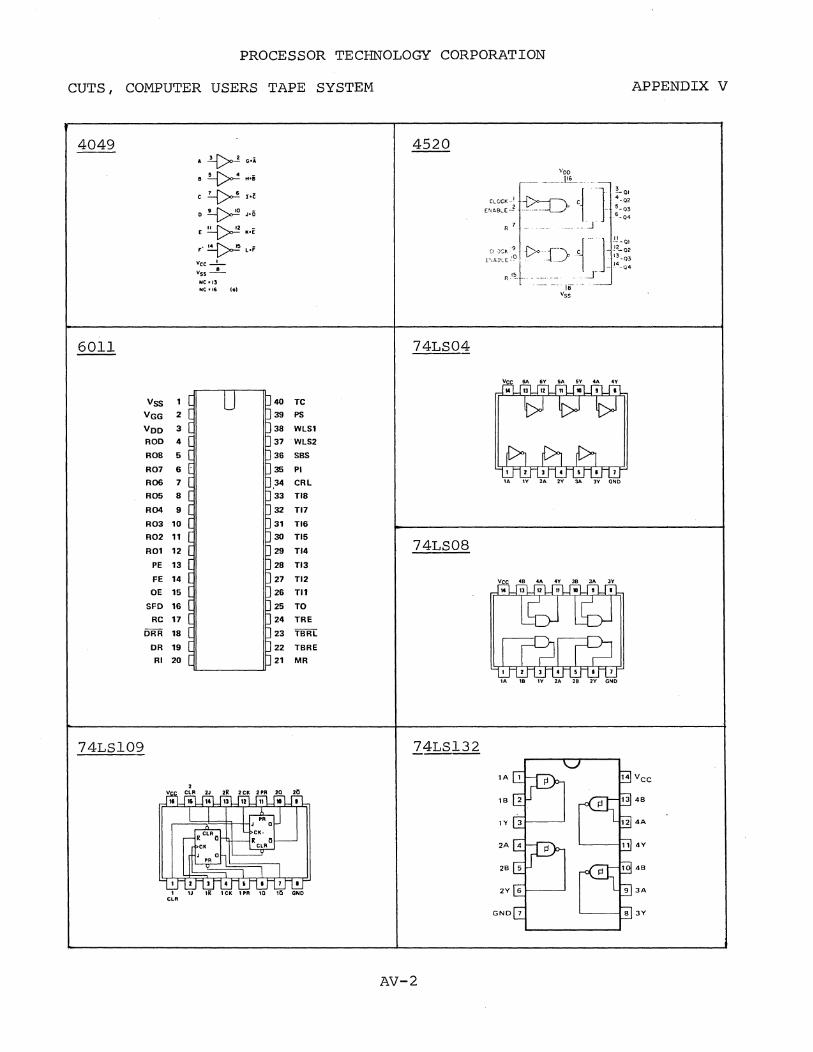
PROCESSOR TECHNOLOGY CORPORATION
CUTS, COMPUTER USERS TAPE SYSTEM
4049
6011
Vss
VGG
VOO ROD
ROB
R07
ROO
R05
R04
R03
R02
R01
PE
FE
OE
SFO
RC
ORR
DR RI
74LS109
2
3
4
5
6 7
B
9
10
11
12
13
14
15
16
17
1B
19 20
~G.i
I~".i
C~%.C
D~".6 ~-
E --.........----- K"E
'·~L.F Vee _,_
vss-e-He -13 Nt -16 c.,
40 TC 39 PS
38 WlS1
37 WlS2
36 SBS
35 PI
34 CRl
33 TIB
32 TI7
31 TI6
30 TI5
29 TI4
2B TI3
27 TI2
26 Tn
25 TO
24 TRE
23 TBRl
22 TBRE 21 MR
1 11 11 t CK 1 PA 10 ,a QND CLO
4520
74LS04
'A IV 'A
74LS08
lA ,. IV
74LS132
AV-2
APPENDIX V
,V 3A 3V GND
ZA ,. 'v GND

PROCESSOR TECHNOLOGY CORPORATION
CUTS, COMPUTER USERS TAPE SYSTEM
74LS136
74LS163
CLEAR LOAD
CK
CLEAR CLOCK ABC 0 ENABLE GNO ~p
DATA INPUTS
74367
78L12
APPENDIX V
74LS155
74LS175
CLEAR 1Q 10 10 20 2li 20 GND
7805uC
BOTTO~ VIEW
AV-3
P SUFFIX PLASTIC PACKAGE
CASE 199-04
Pin 1 Input (Base) Pin 2 Output (Emitter)
Pin 3 Ground (Collector)
Heat sink surface connected to pin 3.

CUTS (Applies only to Rev B and below circuit boards)
ASSEMBLY PROCEDURE CHANGE NOTICE #2
Rev B and below CUTS circuit boards have an error that was introduced during their manufacture: A trace was connected to pin 8 of Ull which shorts the voltage controlled oscillator (VCO) output on pin 4 of Ull to ground. CORRECT THIS ERROR AS SHOWN BELOW BEFORE YOU CHECK THE BOARD AND START ASSEMBLY.
Cut this trace to Pin 8 of Ull to break Ull-4 to ground connection.
UIO
I I I I I I I I II I I
Solder (Back) Side of Board
PROCESSOR TECHNa.oGY CORPORATION 6200 HOLLIS STREET EMERYVILLE CA 94608 (415) 652-8080 CABLE ADDRESS "PROCTEC"

CUTS (Applies only to Rev B and below circuit boards)
ASSEMBLY PROCEDURE CHANGE NOTICE #1
Reference Section II, Step 12, Page II-
Capacitor C31 is a new addition to the CUTS circuitry made after the manufacture of Rev B circuit boards.
On Rev B and below boards, install C31 on the solder (back) side of the board as shown below.
U19
GiiIIIiD
o .. ws
11111
o
Ground
Bottom Pad of R20
__ Solder (Back) Side of Board
__ C31 (470 pfd)
PROCESSOR TECHNOLOGY CORPORATION 6200 HOlLIS STREET EMERYVILLE CA 94608 (415)652-8080 CABLE ADDRESS "PROCTEC"
CUTS MANUAL
ERRATA SHEET #1
Reference Step 23 on Page 11-17
The sixth paragraph should read as follows:
( ) Measure the DC voltage at pin 9 of Ull and write the measured voltage down. (Call this Voltage A.)
The eighth paragraph should read as follows:
( ) Measure the DC voltage at pin 9 of ull and write the measured voltage down. (Call this voltage B.)
MAKE THESE CORRECTIONS IN YOUR MANUAL BEFORE YOU START TO ASSEMBLE
YOUR CUTS MODULE.
ESl-3/77
PROCESSOR TECHNOlOGY CORPORATION 6200 HOllIS STREET EMERYVillE CA 94608 (415) 652-8080 CABlE ADDRESS "PROCTEC"

** **
MANUAL DATA CUTS READ AND WRITE ROUTINES
ALS-8 PROGRAM DEVELOPMENT SYSTEM
PROCESSOR TECHNOLOGY CORP. 62111111 HOLLIS STREET EMERYVILLE, CALIF. 9461118
fHllll1 * 1II1/J'1II2 *
TAPE READ AND WRITE ROUTINES FOR CUTS BOARDS 1111111113 * 1111111114 * 1111111115 * 1111111116 * 1111111117. * THESE ROUTINES WERE EXTRACTED FROM "SOLOS"T'-AND "CUTERu~~ 1111111118 * TO ILLUSTRATE THE REQUIREMENTS OF THE CUTS BOARD FOR 1111111119 * READING AND WRITING TO THE CASSETTE TAPE. BOTH SOLOS AND 11111111/1 * CUTER ALSO HAVE FILE BUFFERING ROUTINES TO PROVIDE BYTE 111011 * BY BYTE TRANSFERS TO THE CASSETTE TAPE. 01/Jl2 * 11111113 * CUTER resides on cassette tape and is available at your 011114 * local Processor Technology Dealer for $11.111111 or ROM 11111115 * resident for use on the GPM module. The CUTER program 11111116 * requires 2K of memory plus'Ik 'of RAM work area. A short 111017 * bootstrap program is used to load CUTER from cassette 11111118 * tape. 111019 * 1111112111 * 11111121 * 11111122 * 1/111123 * 0024 * 11111125'* 11111126 * 11111127 * 11111128 * 11111129 * 1111113111 * 11111131 * 0fiJ32 *
,11111133 * 11111134 * 111035 * 011136 * 11111137 * 111038 * 011139 * 1/104111 '* 1/111141 * 11111142 * 1/111143 * 011144 * 11111145 * 0046 * 111047 * 11111148 * 11111149 * 1111115111 * 11111151 *
CUTER is relocatable to any 256 byte boundary and has a built in command processor and support for serial, parallel, keyboard and VDM I/O as well as CUTS cassette routines. The CUTER software is necessary for all major Processor Technology or Software Technology programs.
CUTER COMMAND LIST
DUMP ENTE~ EXECUTE TLOAD TSAVE TXEQ TCAT CUST SET di SET nu SET ta SET in SET out SET cin SET cout SET xeq SET type
Dump memory Enter to memory Execute a program Load programs or data from cassette Save programs or data to cassette Load and run program from tape List names of files on tape Enter or delete custom command name Set display speed Set output nulls Set tape speed Set input port (0-3) Set output port (111-3) Set custom input driver address Set custom output driver address Set auto execute address to header Set type in header
«=- TAPE READ ROUTINES
PAGE 1
-=»

** ALS-8 PROGRAM DEVELOPMENT SYSTEM **
MANUAL DATA CUTS READ AND WRITE ROUTINES
PROCESSOR TECHNOLOGY CORP. 6200 HOLLIS STREET EMERYVILLE, CALIF. 94608
01iHHl D5 0001 06 03 0003 CD ID 01 0006 DB FB
0008 E5 0009 CD 5F 00 000C El 000D DA 49 00 0010 C2 08 00
0013 E5 0014 11 2D 01 0017 CD 0F 01 001A El 001B C2 08 00
001E Dl 001F 7A 0020 B3 0021 2A 34 01 0024 EB
IIHl25 C2 2B 00 0028 2A 36 01
002B D5
002C 7A 002D B3 002E CA 5A 00 0031 EB
0032 01 00 FF
0052 * 0053 * 0054 * 0055 * 0056 * 0057 * 0058 * 0059 * 0060 * 0061 * 0062 *
ON ENTRY:
ON EXIT:
A HL DE
- HAS UNIT AND SPEED - POINT TO HEADER BLOCK - HAVE OPTIONAL PUT ADDRESS
CARRY IS SET IF ERROR OCCURRED DE HAVE SIZE OF BLOCK READ TAPE UNITS ARE OFF
0063 RTAPE 0064
PUSH MVI CALL IN
D B,3 TON TDATA
SAVE OPTIONAL ADDRESS SHORT DELAY
0065 0066 0067 * LOOP 0068 PTAPI 0069 0070 0071 0072
HERE PUSH CALL POP JC JNZ
UNTIL VALID H RHEAD H
0073 * 0074 0075
FOUND A VALID PUSH
TERR PTAPI HEADER H D,THEAD
0076 0077 0078 0079 * 0080 0081 0082 0083
LXI CALL POP JNZ
FOUND IT •• POP MOV ORA LHLD XCHG
DHCMP H PTAPI
NOW ADJUST D A,D E BLOCK
CLEAR THE UART FLAGS HEADER IS FOUND
HEADER ADDRESS GO READ HEADER
IF AN ERROR OR ESC WAS RECEIVED IF VALID HEADER NOT FOUND
NOW DO CciMPARE GET BACK AND RESAVE ADDRESS
COMPARE DE-HL HEADERS
DIDN T COMPARE ..• GO BACK TO LOOP REGISTERS FOR READ
OPTIONAL PUT" ADDRESS
SEE IF DE IS ZERO GE'I' BLOCK SIZE
•• TO DE 0084 0085 * 0086 0087
DE HAS HBLOCK •.•• HL HAS USER OPTION
0088 * 0089 * 009.0 * 0091 * 0092 * 0093 * 0094 * 0095 * 0096 * 0097 RTAP 0098 * 0099 LOLOOP 0100 0101 0102 0103 * 01.04
JNZ RTAP LHLD LOADR
IF DE WAS ZERO GET TAPE GET TAPE LOAD ADDRESS
THIS ROUTINE READS "DE'" BYTES FROM THE TAPE TO ADDRESS HL. THE BYTES MUST BE FROM ONE CONTIGUOUS PHYSICAL BLOCK ON THE TAPE.
HL HAS ApUTq ADDRESS DE HAS SIZE OF TAPE BLOCK
LOAD ADDRESS
PUSH D SAVE SIZE FOR RETURN TO CALLING PROGRAM
MOV ORA JZ XCHG
LXI
A,D E RTOFF
B,-256
PAGE 2
GET COUNT
COUNT IS ZERO-TURN OFF TAPE AND RETURN GET COUNT TO HL
THIS MANY PRIOR TO CRC TEST

** ALS-8 PROGRAM DEVELOPMENT SYSTEM **
MANUAL DATA CUTS READ AND WRITE ROUTINES
PROCESSOR TECHNOLOGY CORP. 6200 HOLLIS STREET EMERYVILLE, CALIF. 94608
0035 09 0036 D2 4E 00 0039 06 00 1'.103B D3FC
003D 0E 00 003F EB
0040 CD 7D 00 0043 DA 49 00 0046 CA 2C 00
0049 AF 01:':14A 37 004B C3 5B 01:':1
004E 45 004F 21 00 00 0052 C3 3D. 00
1:':1055 06 0.1 0057 CD IF 01 ..
005A AF 005B D3 FA 005D 01 005E C9
1:':105F 06 0A 1:':1061 CD 8F 00
.0064 -D8· 0065 DB FB 0067 B7 0068 C2 5F 00 01:':16B 05 01:':16C C2 61 00
006F CD 9D 01:':1 0072 D8 0073 3D 0.074 C2 6F 00
0105 0106 0107 0108 0109 * 01Hl RDBLK 0111 0112 * 0113 RTLOP 0114 0115 0116 *
DAD JNC MVI OUT
MVI XCHG
CALL JC JZ
0117 * ERROR RETURN 0118 *
.0119 TERR 0120 0121 0122 *
XRA STC JMP
B LBLK B,0 0FCH
RHEDI TERR LOLOOP
A . RTOFI
A LITTLE MATH NO CARRY IT S THE LAST BLOCK 256 TO READ DING THE PORT FOR INSECURE ROBERTS
ZERO THE CRC ROUND ROBIN
READ IN THIS BLOCK IF ERROR OR ESC CONTINUE LOOP IF CRC TEST IS OK
SET ERROR FLAGS
0123 * LAST BLOCK-~PUT FINAL COUNT IN B 0124 * 0125 LBLK 0126 0127 0128 *. 0129 * 0130 TOFF 0131 0132 * 0133 RTOFF 0134 RTOFI 0135 0136
MOV LXI JMP
MVI CALL
XRA OUT POP RET
B" L H,0 RDBLK
B,l DELAY
A STAPT D
READ ~HE HEADER
0137 * 0138 * 0139 * 0140 * 0141 * 0142 RHEAD 0143 RHEAl 1:':1144 0145 0146 0147 0148 0149
MVI CALL RC IN ORA JNZ DCR JNZ
B,10 STAT
TDATA A RHEAD B RHEAl
GET LOWER PORTION OF COUNT TELL DE WE ARE FINISHED
SHORT DELAY AFTER WRITE
TURN OFF THE TAPE RETU~ BYTE COUNT
FIND 10 NULLS
IF ESCAPE IGNORE ERROR CONDITIONS ZERO?
LOOP UNTIL 10 IN A ROW 0150 * 0151 * 0152 * 0153 SOHL 0154
WAIT FOR THE. START CHARACTER
0155 0156 0157 *
CALL RC· DCR JNZ
TAPIN
A SOHL
PAGE 3
ERROR OR ESCAPE
WAIT FOR A 'I

** ALS-8 PROGRAM DEVELOPMENT SYSTEM **
MANUAL DATA CUTS READ AND WRITE ROUTINES
PROCESSOR TECHNOLOGY CbRP. 6200 HOLLIS STREET EMERYVILLE, CALIF. 94608
VJ077 21 2D 01 007A 01 00 10
007D CD 9D fHiJ 0080 D8 0081 77 0082 2'3 0083 CD E6 00 0086 05 0087 C2 7D 00
008A CD 9D 00 008D A9 008E C9
008F DB FA 0091 E6 40
C0 0093 0094 0096 0098 009B 009C
DB FE C2 37 C9
01 IB ,8F IH'J
009D CD 8F 00 00A0 D8
00Al DB FA 00A3 E6 18 00A5 DB FB 00A7 C8 00A8 37 00A9 C9
0158 * 0159 * 0160 * 0161 0162 0163 * 0164 RHEDI 0165 0166 0167 0168 0169 0170 0171 *
NOW GET THE HEADER
LXI LXI
CALL RC MOV INX CALL DCR JNZ
H,THEAD B/ HLEN*256
TAPIN
M,A H UDCRC B RHED1
POINT TO BUFFER LENGTH OF HEADER IN
GET BYTE
STORE IT INCREMENT ADDRESS NOW CALCULATE THE WHOLE HEADER YET? LOOP UNTIL DONE
CRC
B ,C<0
THIS ROUTINE GETS THE NEXT BYTE AND COMPARES IT TO THE VALUE IN REGISTER C. THE FLAGS ARE SET ON RETURN.
01:7 2 * 0173 * 0174 * 0175 * 0176 CRCCK 0177 0.'\..18
CALL XRA RET
TAPIN C
GET CRC BYTE COMPARE IT WITH CALCULATED (CLEAR CARRY)
THIS ROUTINE GETS THE NEXT AVAILABLE BYTE FROM THE TAPE. WHILE WAITING FOR THE BYTE THE KEYBOARD IS TESTED FOR AN ESC COMMAND. IF RECEIVED THE TAPE LOAD IS TERMINATED AND A RETURN TO THE COMMAND MODE IS MADE
0179 * 0180 * 0181 * 0182 * 0183 * 0184 * 0185 * 0186 STAT 0187 0188 0189 0190 0191 0192 0193 0194 * 0195 * 0196 * 0197 TAPIN 0198 0199* 0200 TREDY 0201 02'02 0203 0204 0205 0206 * 0207 * 0208 * 0209 * 0210 *
IN ANI RNZ IN CPI JNZ STC RET'
CALL RC
IN ANI 'IN RZ STC RET
STAPT TDR
KDATA MODE STAT
STAT
STAPT TFE+TOE TDATA
WHEN CHARACTER IS REApy
ESC ?
SET ERROR FLAG AND RETURN
WAIT UNTIL A CHARACTER IS, AVAILABLE
DATA ERROR? GET THE DATA IF NO ERRORS SET ERROR FLAG
WRITE TAPE BLOCK ROUTINE
PAGE 4

** ALS-8 PROGRAM DEVELOPMENT SYSTEM **
NANUAL DATA CUTS ~EAD AND WRITE ROUTINES
PROCESSOR TECHNOLOGY CORP 6200 HOLLIS STREET EMERYVILLE CALIF. 94608
00AA E5 00AB CD ED 00 00AE 1:;1 00AF 11 07 00 00B2 19
00B3 5E 00B4 23 00B5 56 o 0BG. 23 00B7 7E 00B8 23 00B9 66 110BA 6F I<Il!!BB E5
00BC .7A 00BD B3 00BE CA 55 00 00C1 ,01 00 FF 00C4 EB 00C5 09 00C6 D2 04 00 00C9 06 00
00CB 0E 00 00CD EB 00CE CD 02 01 1<10D1 C3 BC 00
00D4 45 0005 21 00 00 00D8 C3 CB 00
00D8 F5 110DC DB FA 00DE E6 80 00E0 CA DC 00 00£:3 Fl 00E4 D3 FB
00E6 91
0211 * 0212 * 0213 * 0214 *
ON ENTRY:
0215 * 0216 WTAPE 0217 0218 0219 0220 0221 * GET 0222-0223 0224 0225 0226 0227 fl228 0229 0230 WRL01 0231 * 0232 *
PUSH CALL POP LXI DAD
ADDRESS MOV INX MOV INX MOV INX MOV MOV PUSH
A - HAS UNIT AND SPEED HL - HAVE POINTER TO HEADER
H SAVE HEADER ADDRESS WHEAD WRITE THE HEADER H D BLKOF OFFSET TO BLOCK SIZE IN HEADER D HL POINT TO BLOCK SIZE
AND SIZE FROM HEADER E,M H D,M H A,M H H,M L,A H
DE HAVE SIZE POINT TO STARTING ADDRESS
HL HAVE STARTING ADDRESS FOR STACK CLEAN UP ON TURN OFF
0233 * THIS ROUTINE WRITES ONE PHYSICAL BLOCK ON THE 0234 * TAPE "DE" BYTES LONG FROM ADDRESS "HL . 0235 * 0236 WRLOP MOV A,D 0237 ORA E TEST IF COUN'T IS ZERO 0238 JZ TOFF 0239 LXI BI -256 SUBTRACT 256 FROM IT 0240 XCHG 0241 DAD B 0242 JNC WLBLK IF 256 WEREN T LEFT 0-243 MVI B,0 0244 * 0245 WDBLK MVI C,0 CRC STARTS WITH ZERO 0246 XCHG RESTORE COUNT TO DE •. ADDRESS TO HL 0247 WDBL1 CALL WLOOP WRITE OUT THE BLOCK 0248 JMP WRLOP AND GO BACK TO MAJOR LOOP 0249 * 0250 WLBLK MOV B,L REMAINDER OF COUNT 0251 LXI H,0 TELL DE WE ARE DONE 0252 JMP WDBLK 0253 * 0254 WRBYT 0255 WRWAT 0256 0257 0258
, 0259
PUSH IN ANI JZ POP OUT
PSW 0FAH 80H WRWAT PSW 0FBH
SAVE CHARACTER GET UART STATUS
WAIT UNTIL IT IS READY
OUTPUT THE CHARACTER
THIS ROUTINE UPDATES THE eRC 0260 * 0261 * 0262 * 0263 UDCRC SUB C FORM PARTIAL
PAGE 5

** ALS-8 PROGRAM DEVELOPMENT SYSTEM **
PROCESSOR TECHNOLOGY CORP MANUAL DATA 6200 HOLLIS STREET CUTS READ AND WRITE ROUTINES EMERYVILLE CALIF 94608
00E7 4F 3264 MOV C,A SAVE IT 00E8 A9 3265 XRA C NOW BEND IT OUT 03E9 2F 3266 CMA GET A FF 00EA 91 0267 SUB C CRC+1-1 IS NOT THE SAME 03EB 4F 0268 MOV C,A AND RESAVE IT 00EC C9 0269 RET
3270 * 0271 * 0272 * THIS ROUTINE WRITES THE HEADER POINTED TO BY 0273 * HL TO THE TAPE. 0274 *
00ED CD 1B 01 0275 WHEAD CALL WTON TURN ON THE TAPE AND DELAY 00F0 16 32 0276 MVI D,50 WRITE 50 ZER0S 00F2 AF 0277 NULOP XRA A 00F3 CD DB 30 0278 CALL WRBYT 00F6 15 0279 DCR D 1iJ0F7 C2 F2 30 0280 JNZ NULOP
0281 * 03FA 3E 01 0282 MVI A.1 50 ZER0S FOLLOWED BY A ONE 00FC CD DB 30 0283 CALL WRBYT 00FF 01 00 10 0284 LXI B,HLEN*256 HEADER LENGTH TO B, ZERO TO C
0285 * 0102 7E 0286 WLOOP MOV A,M GET CHARACTER 0103 CD DB 00 0287 CALL WRBYT WRITE IT TO THE TAPE 0106 05 0288 DCR B 0107 23 0289 ;I:NX H 0108 C2 02 01 f/j290 JNZ WLOOP 010B 79 0291 MOV A,C GET CRC 0HlC C3 DB 00 0292 JMP WRBYT PUT IT ON THE TAPE AND RETURN
0293 * 0294 * 0295 * THIS ROUTINE COMPARES THE HEADER IN THEAD TO 3296 * THE USER SUPPLIED HEADER ADDRESS IN HL. 0297 * ON RETURN IF ZERO IS SET IF THE TWO NAMES COMPARED 0298 *
fill 0 F 06 35 0299 DHCMP MVI B,5 COMPARE FIVE CHARACTERS 01ll lA 0300 DHLOP LDAX D GET ONE PART 0112 BE 0301 CMP M COMPARE IT WITH THE OTHER 0113 C0 0302 RNZ RETURN IF NOT THE SAME 0114 05 0303 DCR B 0115 C8 0304 RZ IF ALL FIVE COMPARED 0116 23 0305 INX H COMPARE THE NEXT 0117 13 3306 INX D 0118 C3 II I'll 0337 JMP DHLOl:?
3308 * 3339 *
3llB 06 04 0310 WTON MVI B,4 SET LOOP DELAY 3llD D3 FA 03ll TON OUT STAPT TURN ON THE SELECTED DRIVE
3312 * 3llF II 00 00 0313 DELAY LXI D,3 0122 1B 0314 DLOP1 DCX D 0123 7A 0315 MOV A,D 3124 B3 3316 ORA E
PAGE 6
MANUAL DATA CUTS READ AND WRITE ROUTINES
0125 C2 22 III 0128 105 10129 C2 IF 101 l?i12C C9
012D 10132 0133 10134 10136 10138 1H3A
Ilkl FA 010 FB 1010 101 1010 1B
kll?i 108 1010 110 00 410 010 80
0kl 410 .010 810
1010 10 1010 107
10·317 10318 10319 103210 10321 * 10322 * 10323 * 10324 * 10325 * 10326 * 10327 * 10328 * 10329 STAPT l?i33kl TDATA 10331 KDATA 10332 MODE 0333 * 10334 * 0335 * 10336 * 10337 * 10338 * 10339 TFE 10340 TOE 10341 TDR 0342 TTBE 10343 * 10344 TAPE1 10345 TAPE2 10346 * 10347 * 10348 * 10349 * 10350 * 10351 * 10352 * 10353 * 10354 * 10355 * 0356 * 10357 * 10358 THEAD 10359 103610 HTYPE 10361 BLOCK 10362 LOADR 10363 XEQAD 10364 HSPR 0365 * 10366 HLEN 10367 BLKOF 10368 * 10369 *
** ALS-8 PROGRAM DEVELOPMENT SYSTEM **
JNZ OCR JNZ RET
PROCESSOR TECHNOLOGY CORP 621010 HOLLIS STREET EMERYVILLE, CALIF. 946108
DLOP1 B DELAY
LOOP HERE UNTIL DE ARE ZERO
LOOP HERE UNTIL B IS ZE.RO
PORT ASSIGNMENTS
EQU l?iFAH EQU filFBH EQU 1 EQU 1BH
STATUS PORT GENERAL TAPE DATA KEYBOARD DATA PORT FOR ESCAPE TEST ESCAPE KEY
BIT ASSIGNMENT MASKS
EQU EQU EQU EQU
EQU EQU
DS DS DS DS DS DS DS
EQU EQU
8 16 64 128
64 128
GLOBAL AREA
TAPE FRAMING ERROR TAPE OVERFLOW ERROR TAPE DATA READY TAPE TRANSMITTER BUFFER EMPTY
TAPE ONE OFF BIT TAPE TWO OFF BIT
SYSTEM PARAMETER AREA
5 1 1 2 2 2 3
NAME THIS BYTE MUST BE ZERO FOR AUTO EXECUTE TYPE BLOCK SIZE LOAD ADDRESS AUTO EXECUTE ADDRESS SPARES
$-THEAD LENGTH OF HEADER BLOCK-THEAD OFFSET TO BLOCK SIZE
PAGE 7

** . ALS-8 PROGRAM DEVELOPMENT SYSTEM **
PROCESSOR TECHNOLOGY CORP. r MANUAL DATA 6200 HOLLIS STREET ',-
CUTS READ AND WRITE ROUTINES EMERYVILLE, CALIF. 94608
0370 *
BLKOF 0007 0219 BLOCK 0134 0083 0367 .' CRCCK 008A DELAY 011F 0131 0319 DHCMP 010F 0076 DHLOP 0111 0307 DLOPI 0122 0317 HLEN 0011" 0162 0284 HSPR 013A HTYPE 0133 KDATA 0001 0189 LBLK 004E 0106 LOADR 0136 0087 LOLOO 002C 0115 MODE 001B 0190 NULOP 00F2 0280 PTAPI 0008 0072 0078 RDBLK 003D 0127 RHEAl 0061 0149 RHEAD 01iJ5F 0069 0147 RHEDI 007D 0113 0170 RTAP 002B 0086 RTAPE 0000 RTLOP 0040 RTOFI 005B 0121 RTOFF 005A 0101 SOHL 006F 0156 STAPT 00FA 0134 0186 0200 0311 STAT 008F 0143 0191 0197 TA.l:'El 0040 TAPE2 0080
C~I TAPIN 009D '0153 0164 0176 TDATA 00FB 0066 01'45 0202 TDR 0040 0187 TERR 00·49 0071 0114 TFE 0008 0201 THEAD 012D 0075 0161 0366 0367 TOE 0010 0201 TOFF 0055 0238 TON 011D 0065 TRBDY 00Al TTBE 0080 UDCRC 00E6 0168 wDBLl 00CE WDBLK 00CB 0252 WHEAD 00EO 0217 WLBLK 0004 0242 WLOOP 0102 0247 0290 WRBYT 000B 0278 0283 0287 0292 WRLOI 00BB WRLOP 00BC 0248
( PAGE 8

MANUAL DATA CUTS READ AND WRITE ROUTINES
WRWAT WTAPE WTON XEQAD
0L1DC L10AA 011B 0138
0257
0275
** ALS-8 PROGRAM DEVELOPMENT SYSTEM
PROCESSOR TECHNOLOGY CORP. 6200 HOLLIS STREET EMERYVILLE CALIF. 94608
PAGE 9
**