Current through electronic device. Dynamics of electronic carriers J = nev d = ne 2 F /m* J = F...
56
Current through Current through electronic device electronic device
-
Upload
frederica-preston -
Category
Documents
-
view
214 -
download
0
Transcript of Current through electronic device. Dynamics of electronic carriers J = nev d = ne 2 F /m* J = F...

Current through Current through electronic deviceelectronic device

Dynamics of electronic Dynamics of electronic carrierscarriers
J = nevd = ne2F/m* J = F (lei de Ohm)
= ne2/m* = ne
vd = F
= e/m*
= e(nee + npp)
meFvdt
dd /
r
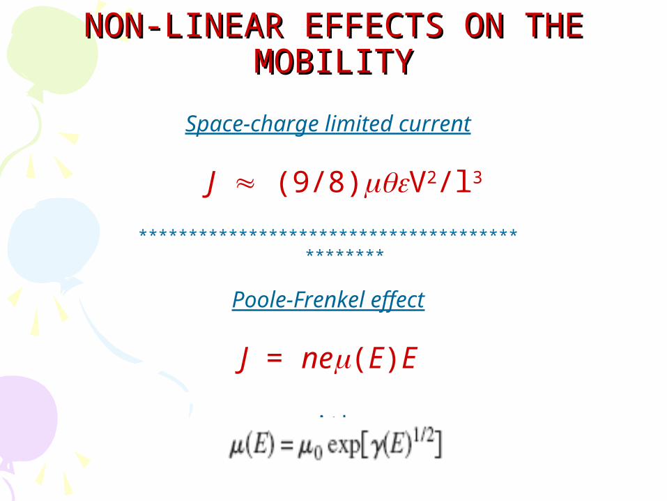
NON-LINEAR EFFECTS ON THE NON-LINEAR EFFECTS ON THE MOBILITYMOBILITY
Space-charge limited current
J (9/8)V2/l3
**********************************************
Poole-Frenkel effect
J = ne(E)E
with
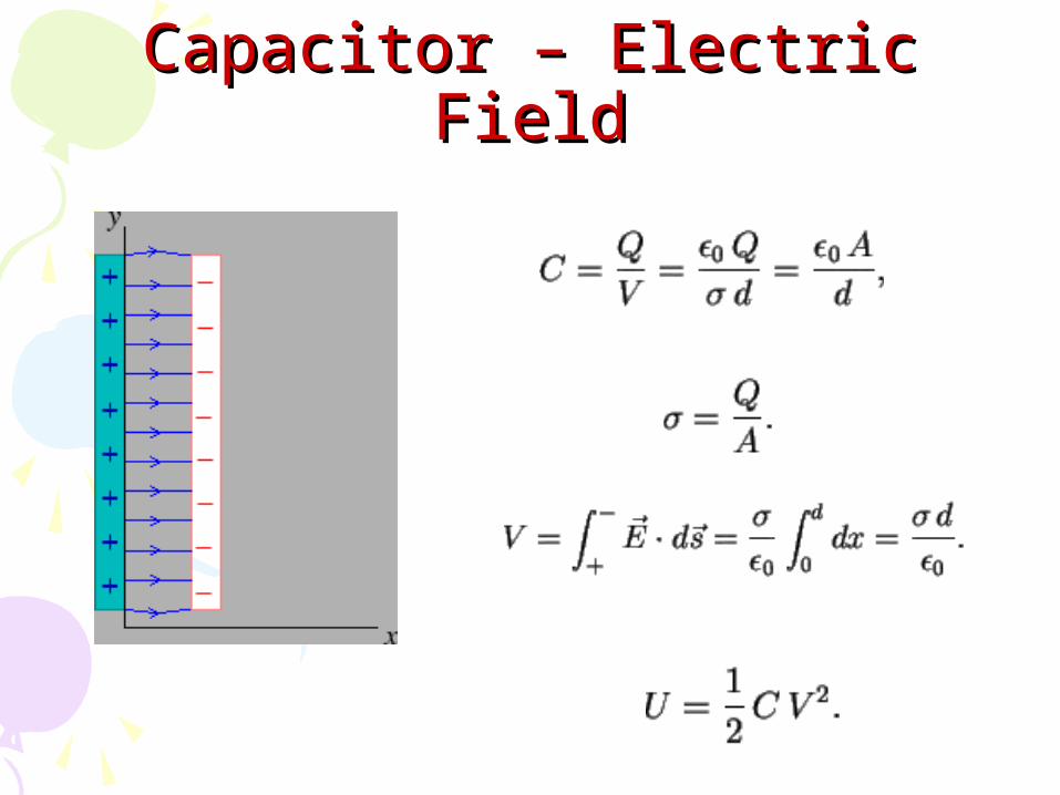
Capacitor – Electric FieldCapacitor – Electric Field

Dielectrics - PolarizationDielectrics - Polarization

Dipole MomentDipole Moment
= 2a

DEVICE 3: OTFTsOrganic Thin-Film Transistors
DEVICE 2: OLEDsOrganic Light-Emitting Diodes
DEVICE 1: OPVsOrganic Photovoltaics

DEVICE 1: DEVICE 1: OPVOPVOOrganic rganic PPhotohotovvoltaicsoltaics

Generations of Solar Cells
First: PV p-n junction diode of crystalline silicon (market)
Second: PV thin films of non-monocrystalline semiconductors(amorphous silicon, poly-crystalline silicon, cadmium
telluride films, copper indium selenide/sulfide,...) (market)
Third: Organic photovoltaic cells, photoelectrochemical cells, dye-sensitized Solar cells,...) (research)
Fourth: Biomolecular cells (prevision) - Mimicking the nature.

MARKETMARKET
P V T e c h n o l o g y P VG e n e r a t i o n
F o r e c a s t t i m e f r o m m a r k e ta c c e p t a n c e t o d e c l i n e
S i l i c o n C r y s t a l l i n e 1 1 9 7 0 - 2 0 2 0S i l i c o n A m o r p h o u s 2 1 9 8 3 - 2 0 2 5S i l i c o n T h i n F i l m 2 2 0 0 1 - 2 0 5 0C d T e 2 1 9 9 5 - 2 0 1 0C I S / C I G S o t h e r 3 / 5 , 2 / 4 / 6 2 2 0 0 0 - 2 0 5 0D S C 3 2 0 0 3 - 2 0 5 5D S C - h y b r i d 3 + 2 0 1 5 - 2 1 0 0O r g a n i c - h y b r i d 3 + 2 0 1 5 - 2 1 0 0B i o l o g i c a l 4 2 0 3 0 - 2 1 0 0 +
A c t u a l o r f o r e c a s t m a r k e t a c c e p t a n c e t o m a r k e t d e c l i n e f o r t h e i m p o r t a n t P V t e c h n o l o g i e s
T i m i n g

Sun: Total Sun: Total powerpower
0
/inP A F hc d
Organic materialAbsorption
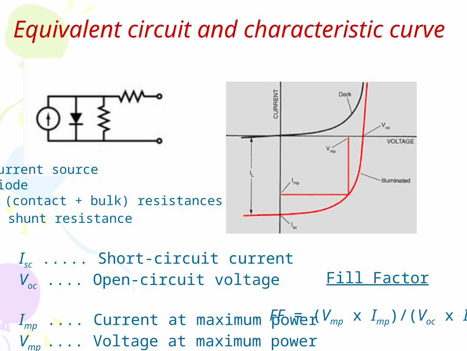
Equivalent circuit and characteristic curve
Isc ..... Short-circuit currentVoc .... Open-circuit voltage
Imp .... Current at maximum powerVmp .... Voltage at maximum power
Fill Factor
FF = (Vmp x Imp)/(Voc x Isc)
Current sourceDiodeRc (contact + bulk) resistancesRs shunt resistance

.out mp mp ca ccP V I FF V I
EFFICIENCY

EfficiencyEfficiency
Quantum efficiency: ratio of the number of collected chargecarriers to the number of incident photons (EQE or IPCE).
Power Conversion Energy (PCE):ratio between the solar power produced by the cell by the power of the incidente flux of light


First generation: pn JUNCTION
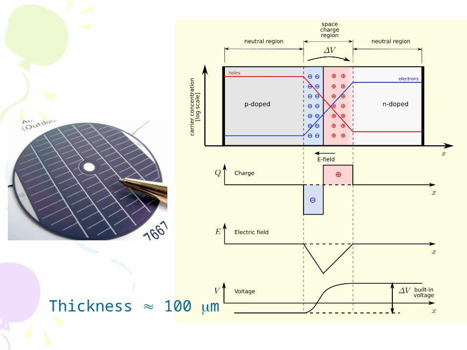
Thickness 100 m

Second generation: Inorganic Heterojunction
Thickness 5 m

Third generation: Organics

ELECTRONIC DEFECTS
Poly(p-phenylene) - PPP
Charge Charge spinspin
exciton singlet 0 0
Negative polaron - e 1/2
Positive polaron e 1/2
Negative bipolaron - 2e 0
Positive bipolaron 2e 0
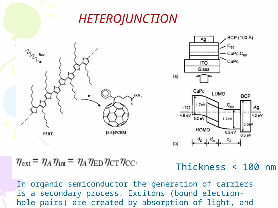
In organic semiconductor the generation of carriers is a secondary process. Excitons (bound electron-hole pairs) are created by absorption of light, and should be dissociated, and then the carriers collected by electrodes)
HETEROJUNCTION
Thickness < 100 nm

2.5 % Efficient Organic Plastic Solar Cells
S. E. Shaheen et al, Appl. Phys. Lett 78, 841 (2001)
First High EfficiencyFirst High Efficiency

Dispersed electronegative species

Poly(disilanyleneoligothienylene) + CPoly(disilanyleneoligothienylene) + C6060
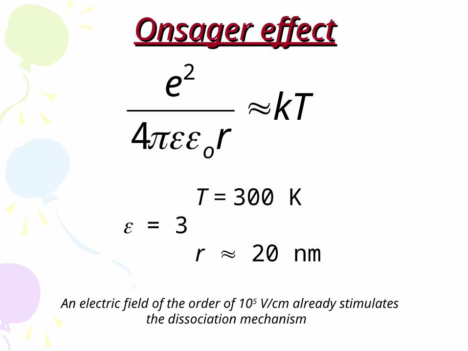
Onsager effectOnsager effect
kTr
e
o
4
2
T = 300 K = 3 r 20 nm
An electric field of the order of 105 V/cm already stimulatesthe dissociation mechanism
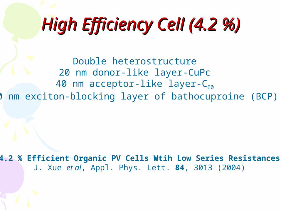
High Efficiency Cell (4.2 %)High Efficiency Cell (4.2 %)
4.2 % Efficient Organic PV Cells Wtih Low Series ResistancesJ. Xue et al, Appl. Phys. Lett. 84, 3013 (2004)
Double heterostructure20 nm donor-like layer-CuPc40 nm acceptor-like layer-C60
10 nm exciton-blocking layer of bathocuproine (BCP)

High efficiency cell (4.6 %)High efficiency cell (4.6 %)
Poly(ethylenedioxythiophene):polystyrenesulfonatePoly(3-hexylthiophene-2,5-diyl):[6,6]-phenil-C61-butyric acid methyl esterCopper phthalocyanine:fullerene
High efficient organic tandem solar cells using naimproved connecting architecture
A.G. F. Janseen et al, Appl. Phys. Lett. 91, 073519 (2007)

Donor-acceptor mixture

Important characteristicsImportant characteristics
Characteristics of OPV:
High absorption coefficient (10-5 cm-1)Short penetration depthThin films (10 – 1000 nm)
Important limitation for organic PV isthe short diffusion length of the exciton

To mentionTo mention
Electrochemical Solar CellElectrochemical Solar Cell

Summary

OPV End

DEVICE 2: OLEDsOrganic Ligth-Emittng Diodes
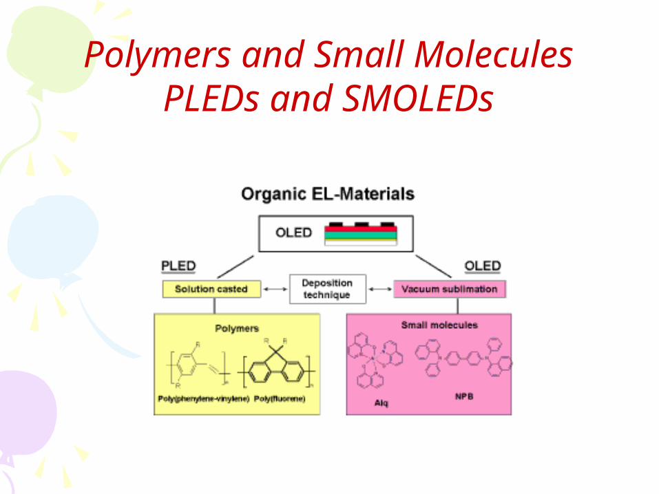
Polymers and Small MoleculesPLEDs and SMOLEDs

Most important luminescent polymers
Poly(p-phenylene vinylene)
Polyfluorene

Most important luminescent small molecules
ALq3 Pentacene derivatives

Most important electrical Most important electrical and optical characteristicsand optical characteristics

IV curves IV curves
ITO/PPV/Al ITO/MH-PPV/Al

Current vs LuminescenceCurrent vs Luminescence
40 45 500
1
2
3
4
T = 20 K
Intensidade Luminosa (U
.A.)
Corrente
Cor
rent
e (m
A)
Voltagem (V)
Intensidade luminosa

JABLONSKI DIAGRAMJABLONSKI DIAGRAM

Absorption and Emission (molecules)Frank-Condon Efeect

Absorption and Emission Absorption and Emission of PPVof PPV
200 300 400 500 600 700 800
Comprimento de onda (nm)
PL
(u
.a.)
547 nm
437 nm
Ab
sorção (
u.a
.)

Photo and Electroluminescent emissionPhoto and Electroluminescent emission

480 510 540 570 600 630 660 690
Comprimento de Onda (nm)
P1= (//) e P
2 = (//)
P1= () e P
2 = ()
Inte
nsid
ade
de E
mis
são
(u.a
)
Detecteur0º
180º
90º
Analisateur
P1 (//)
S-Film
P1 ()
Laser
Optical system to detect polarized photoluminescence

Disordered PPV Film
0 60 120 180 240 300 360
0,2
0,4
0,6
0,8
1,0
1,2
1,4
P1(//)P1()
Inte
nsid
ade
de E
mis
são
Nor
mal
iz. (
u.a.
)
Ângulo do Analisador P2 (Grad)
0 60 120 180 240 300 360
0,2
0,4
0,6
0,8
1,0
1,2
1,4
0 60 120 180 240 300 360
0,2
0,4
0,6
0,8
1,0
1,2
1,4
P1(//)P1()
Inte
nsid
ade
de E
mis
são
Nor
mal
iz. (
u.a.
)
Ângulo do Analisador P2 (Grad)
0 60 120 180 240 300 360
0,4
0,6
0,8
1,0
1,2
P1(//)P1()
Inte
nsid
ade
de E
mis
são
Nor
mal
iz.(
u.a.
)
Ângulo do Analisador (Grad)
0 60 120 180 240 300 360
0,4
0,6
0,8
1,0
1,2
0 60 120 180 240 300 360
0,4
0,6
0,8
1,0
1,2
P1(//)P1()
Inte
nsid
ade
de E
mis
são
Nor
mal
iz.(
u.a.
)
Ângulo do Analisador (Grad)
Stretched PPV Film

Stretched PPVStretched PPV
-50 0 50 100 150 200 250 300 350 400
0.6
0.7
0.8
0.9
1.0
1.1
1.2
1.3
1.4
4.0 mm A
A
Inte
ns
ida
de
(u
.a)
Ângulo (graus)
-50 0 50 100 150 200 250 300 350 400
0.6
0.7
0.8
0.9
1.0
1.1
1.2
1.3
1.4 3.5 mm A
AIn
ten
sid
ad
e (
u.a
.)
Ângulo (u.a.)
-50 0 50 100 150 200 250 300 350 4000.6
0.7
0.8
0.9
1.0
1.1
1.2
1.3
1.43.0 mm
A
A
Inte
ns
ida
de
(u
.a.)
Ângulo (graus)
-50 0 50 100 150 200 250 300 350 4000.6
0.7
0.8
0.9
1.0
1.1
1.2
1.3
1.4 2.5 mm A
A
Inte
ns
ida
de
(u
.a.)
Ângulo (graus)
-50 0 50 100 150 200 250 300 350 4000.6
0.7
0.8
0.9
1.0
1.1
1.2
1.3
1.4 2.0 mm A
A
Inte
ns
ida
de
(u
.a.)
Ângulo (graus)
-50 0 50 100 150 200 250 300 350 400
0.7
0.8
0.9
1.0
1.1
1.2
1.3
1.4
A
A
Inte
ns
ida
de
(u
.a.)
Ângulo (graus)
1.0 mm
-50 0 50 100 150 200 250 300 350 4000.6
0.7
0.8
0.9
1.0
1.1
1.2
1.3
1.4 1.5 mm A
A
Inte
ns
ida
de
(u
.a.)
Angulo (graus)
-50 0 50 100 150 200 250 300 350 4000.7
0.8
0.9
1.0
1.1
1.2
1.3
1.4
Inte
ns
ida
de
(u
..a
)
Ângulo (graus)
A
A
0.0 mm

Electronic Model and Distribution of conjugation lenght PPV
(a) (b)(a) (b)

TECHNOLOGYTECHNOLOGY


PLEDs – Blue and WhitePLEDs – Blue and White

Ink Jet Printing ProcessInk Jet Printing Process
Ink-Jet Printer Heads
PLEDs are solution processable, and can be appliedusing ink jet printing processes

Printers
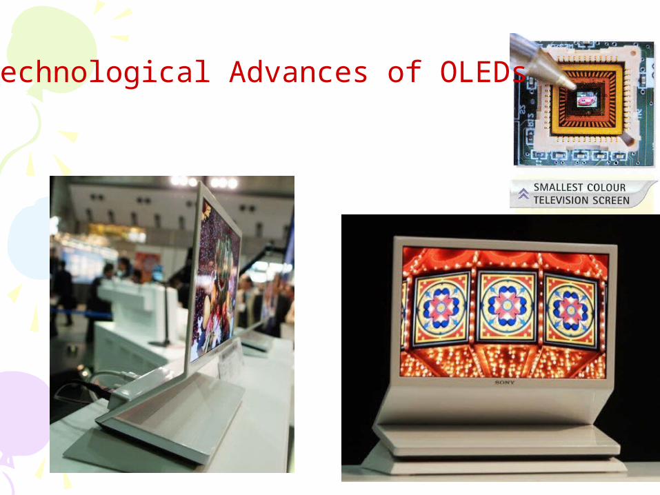
Technological Advances of OLEDs

Future? No, present!Future? No, present!
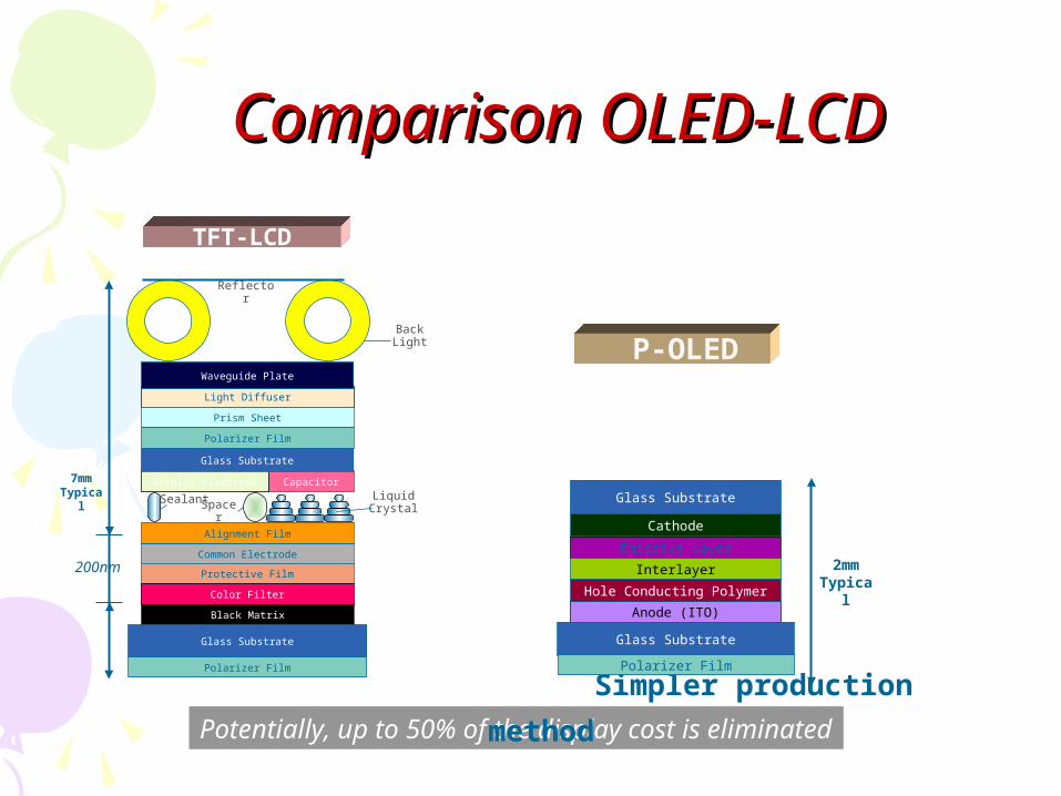
Comparison OLED-LCDComparison OLED-LCD
Light Diffuser
Prism Sheet
Polarizer Film
Common Electrode
Protective Film
Glass Substrate
Waveguide Plate
Back Light
Reflector
Polarizer Film
Black Matrix
Color Filter
Capacitor
Alignment Film
Liquid CrystalSpace
r
Sealant
7mm Typica
l
TFT-LCD
Potentially, up to 50% of the display cost is eliminated
P-OLED devices can reduce
costs significantly:
No backlight unit
No liquid crystal light
valve
No color filter
Simpler bill of
materials
Simpler production
method
Display Electrode
Glass Substrate
2mm Typica
l
Cathode
Anode (ITO)
Glass Substrate
P-OLED
Glass Substrate
Polarizer Film
Emissive Layer
Interlayer
Hole Conducting Polymer
200nm

White OLED (Organic White OLED (Organic Lighting)Lighting)