Current and Future Manufacturing Test Solution...
28
Current and Future Manufacturing Test Solution Strategies - Boundary Scan and Board Assisted-BIST Speaker: Eugene Lin, Agilent October 26, 2012 iNEMI Session, IMPACT
Transcript of Current and Future Manufacturing Test Solution...

Current and Future Manufacturing Test Solution Strategies
- Boundary Scan and Board Assisted-BIST
Speaker: Eugene Lin, Agilent
October 26, 2012
iNEMI Session, IMPACT

iNEMI Projects on Test Technology
• Boundary Scan Project
Chairs: Phil Geiger, Dell; Steve Butkovich, Cisco
– Phase 1: Industrial Survey – Boundary Scan Adoption
– Phase 2: Structural Test of External Memory Devices
1
• Built in Self Test (BIST) Project
Chair: Zoe Conroy, Cisco
– Phase 1: Survey IC BIST current and future adoption at board test
– Phase 2: Survey Use-case generation for standardization
– Phase 3: Standardization to drive industry standard changes (to
“standardize” BA-BIST on two use-cases: HSIO (chip to chip), ASIC to
external memory)
iNEMI Boundary Scan and BIST Projects
Participating Members

Boundary Scan Project Introduction
• Gap identified by the 2009 iNEMI Boundary-Scan survey: – Over 80% of board test engineers struggle to implement boundary-scan based
connectivity testing on soldered down SRAM/DRAM memory devices with no
on-chip testability (excluding DIMMs and other plug-in memory).
• Structural connectivity test of external memory devices is a
“crisis in waiting” as memory devices get larger and faster. – Loss of standard test point access due to circuit density and signal integrity
concerns
– Memory signal/speed timing requirements exceed capability of test equipment
– No “test mode” designed into memory devices to allow easy, straightforward
generation of a structural test
• Without a comprehensive structural test to find and diagnose
failures, functional board test (FT) must take up the slack.
• Assembly and test costs increase!
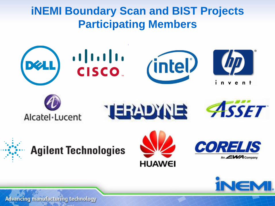
Introduction - Typical DRAM Memory Scenario
Memory
Controller
1149.X
compliant
DRAM
DRAM
DRAM
DRAM
Today: DDR3
G-DDR3
G-DDR5
LP-DDR1
LP-DDR2
Tomorrow: DDR4
G-DDR6
LP-DDR3 Can be a CPU or
an independent
memory
controller
All ICs are SMT
Memory soldered down
No TP access to A/D bus
No TP access to Memory
clock pins

Boundary Scan (Structural Test of External
Memory Devices) Project Purpose
• Project Teams were formed within iNEMI
– Evaluate
• current and upcoming boundary-scan related test methods
• current and upcoming DFT technology solutions
– Pros, cons, limitations
– Determine current and future Best Practices using combinations of test
methods and DFT technologies
– Increase industry awareness of the following:
• Boundary Scan Methods and Availability in Devices
• Work with Standards Organizations in providing a standard method of
controlling and use of boundary scan and Built in Self Test (BIST)
• DFT technologies

Overview of Test Methods and Strategies
• ICT - Full net access
• ICT Integrated Boundary-scan
• Powered Opens at ICT
• Stand-alone Boundary-scan
• Processor Controlled Test
• Board Level BIST
– FPGA Driven BIST
• IEEE 1149.1Standard
• IEEE 1149.6 Standard
• IEEE 1581 – 2011 Standard
• IEEE 1149.8.1- 2012
Standard
• IEEE P1687 Standard under
Development
• Embedded capacitive sense
plate (ECSP)
Test Methods DFT Strategies
Methods/Strategies fall into two categories

Test Methods and Strategies
ICT – full access to the circuit •“Traditional” method of test – our baseline for test coverage
•Timing requirements significantly limits test coverage for many current devices and future devices
ICT Integrated Boundary-scan •Software for ICT systems that uses ICT pin electronics to perform IEEE 1149.x boundary-scan testing of scan chains
•Test speed limited by ICT pin electronics
Test Methods and Strategies
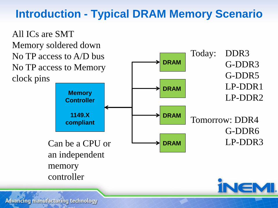
IEEE 1581 – 2011 Standard • Method for static interconnect testing of memory devices
• IEEE 1581 test mode bypasses the functional memory core and
places combinatorial logic between the device inputs and outputs
IEEE 1581 Device
Memory Cells
Combinational
Test Logic
Memory Controller
Test control
Transparent Test
Mode (optional)
Control
Device
- IEEE
1149.1
Compliant
Input
Bus
Output
Bus
x
y
XOR
Test Methods and Strategies
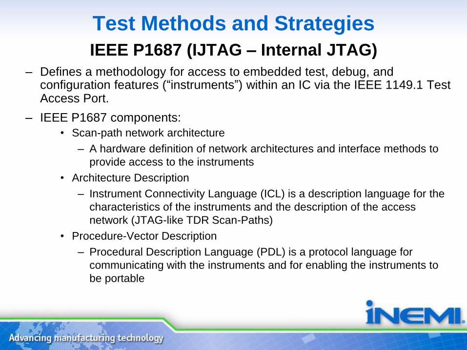
IEEE P1687 (IJTAG – Internal JTAG)
– Defines a methodology for access to embedded test, debug, and configuration features (“instruments”) within an IC via the IEEE 1149.1 Test Access Port.
– IEEE P1687 components:
• Scan-path network architecture
– A hardware definition of network architectures and interface methods to
provide access to the instruments
• Architecture Description
– Instrument Connectivity Language (ICL) is a description language for the
characteristics of the instruments and the description of the access
network (JTAG-like TDR Scan-Paths)
• Procedure-Vector Description
– Procedural Description Language (PDL) is a protocol language for
communicating with the instruments and for enabling the instruments to
be portable

Test Methods and Strategies
Powered Opens
• Used on ICT systems supporting powered opens techniques
• Combines capacitive opens techniques and boundary scan

Test Methods and Strategies
Processor Controlled Test (PCT)
• Compatible with
– IEEE 1581
– JEDEC Scan
– IEEE P1687
• However, it’s not practical to use those technologies at PCT
– Access to devices is made by conventional functional means through
the processor
• Specific DFT in memory devices is not strictly required
– They would be implemented at stand-alone boundary-scan, which
precedes PCT in the PCBA test process
• PCT can be a powerful tool to test memory, but the new DFT technologies
do not add any additional value to it.

12
Test Methods and Strategies
JTAG Module
To TAP
Stand-alone IEEE 1149.x Boundary-scan
• Traditional benchtop boundary-scan testing
– PC driven test using a JTAG module to exercise scan chains

13
Test Methods and Strategies
Processor Controlled Test (PCT)
•Access and control on-board CPU through the debug port
•At-speed testing of anything the processor can reach
JTAG/PCT Module
To TAP

Test Methods and Strategies
Embedded capacitive sense plate (ECSP) •Used with capacitive opens test methods
•Build the capacitive opens sense plate into the IC package
Fill metal (black) is added for thermal
connectivity and mechanical coplanarity.
• Electrically floating
• Has small capacitance to IC signal
nets
Figures adapted from US Patent Application Publication US2005/0253616 A1, Nov 2005. (This is a
publication; the technology is not patented.)
Connect fill metal areas that couple to DUT signals.
Bring a connection point to a surface area for our
conventional sense plate to couple with.

DFT Technologies Alignment with Test
Methods
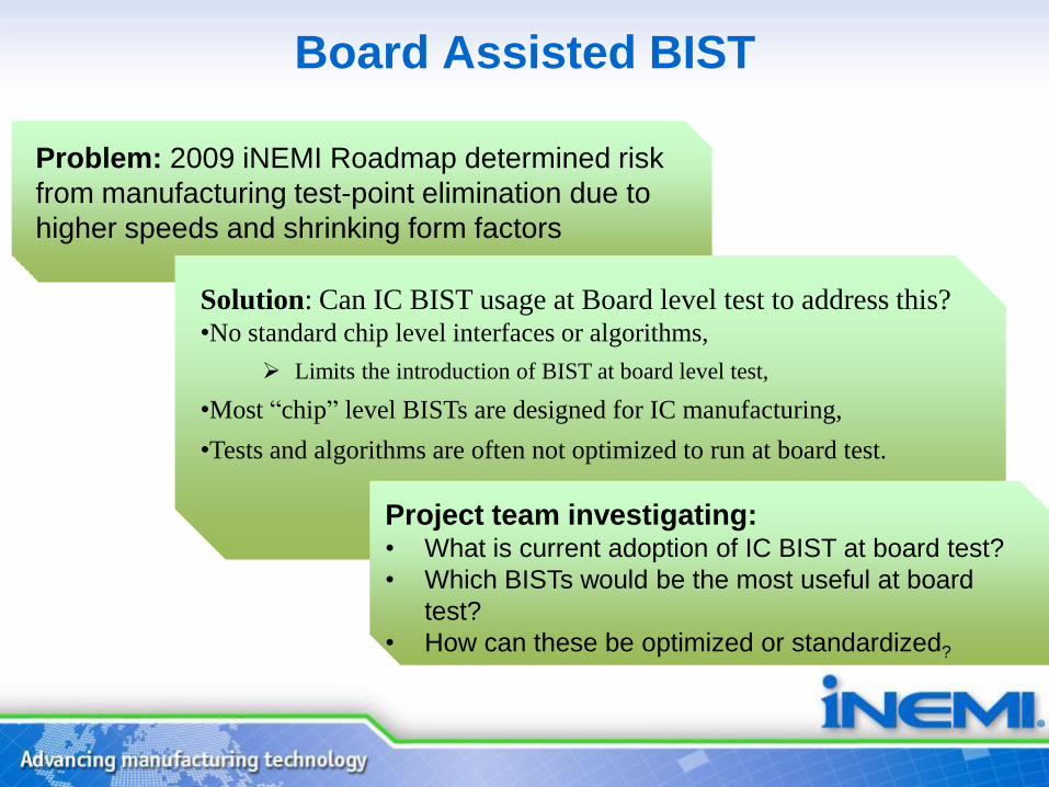
Board Assisted BIST
Problem: 2009 iNEMI Roadmap determined risk
from manufacturing test-point elimination due to
higher speeds and shrinking form factors
Solution: Can IC BIST usage at Board level test to address this? •No standard chip level interfaces or algorithms,
Limits the introduction of BIST at board level test,
•Most “chip” level BISTs are designed for IC manufacturing,
•Tests and algorithms are often not optimized to run at board test.
Project team investigating: • What is current adoption of IC BIST at board test?
• Which BISTs would be the most useful at board
test?
• How can these be optimized or standardized?

Board Assisted BIST Definition
Board-Assistance BIST is an embedded capability
within an IC that is fully or partially self-contained,
in that it incorporates some or all of the following
capabilities:
• pattern/signal generation,
• pattern/signal delivery,
• response or data capture,
• response evaluation functions.
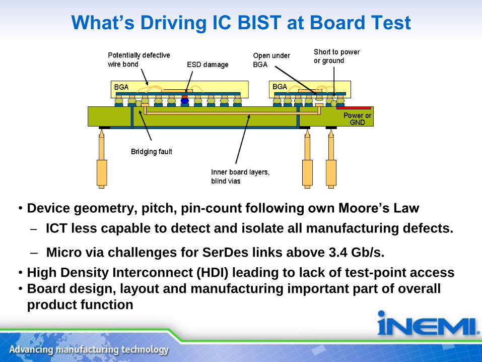
What’s Driving IC BIST at Board Test
• Device geometry, pitch, pin-count following own Moore’s Law
– ICT less capable to detect and isolate all manufacturing defects.
– Micro via challenges for SerDes links above 3.4 Gb/s.
• High Density Interconnect (HDI) leading to lack of test-point access
• Board design, layout and manufacturing important part of overall
product function
0
10
20
30
40
50
60
70
1st problem 2nd problem 3rd problem
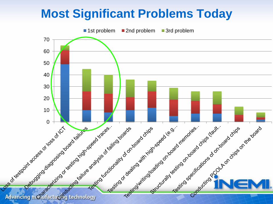
Most Significant Problems Today
0
5
10
15
20
25
30
35
40
45
50
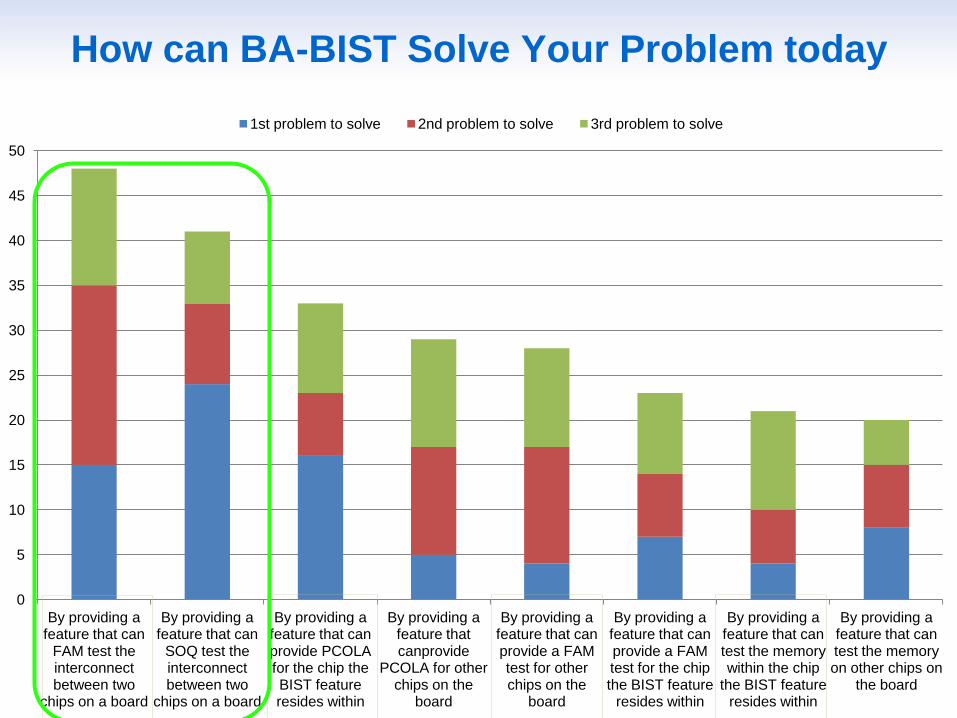
By providing a feature that can
FAM test the interconnect between two
chips on a board
By providing a feature that can
SOQ test the interconnect between two
chips on a board
By providing a feature that can provide PCOLA for the chip the BIST feature resides within
By providing a feature that canprovide
PCOLA for other chips on the
board
By providing a feature that can provide a FAM test for other chips on the
board
By providing a feature that can provide a FAM test for the chip the BIST feature
resides within
By providing a feature that can test the memory within the chip
the BIST feature resides within
By providing a feature that can test the memory on other chips on
the board
1st problem to solve 2nd problem to solve 3rd problem to solve
How can BA-BIST Solve Your Problem today

Test Environments Where Most
Issues Occur
0
10
20
30
40
50
60
70
80
Manufacturing board test
New product introduction
Board debug and diagnosis
Field return evaluation
Board yield analysis
Other
1st problem area 2nd problem area 3rd problem area

• Many IC BIST tests are available and run at board level
– 60% Board designers are requesting access to IC BIST
• Most needed BA-BIST functions are:
– To test external memories
– BIST Pattern generators to drive data off chip
– HSIO-BIST to provide pattern to/through the PHY of a chip
• Access is predominantly via IEEE1149.1 TAP
• Majority of BIST tests are proprietary
– Potential roadblock to wider adoption and implementation
• BIST run at the board level is good at catching defects
• Main areas of use: manufacturing board test, NPI, board debug
and diagnosis
Survey Key Takeaways

• However, some issues encountered:
– Some ICs do not support BIST function,
– IC suppliers often do not give BIST function to board users,
– Lack of access when IC is mounted on the board,
– BIST function at board test not supported by a standard.
• Looking to the future:
– Seen to be critical for future fault isolation,
– Would like BIST coverage to be > 80% at board test
– > 75% respondents see BIST coupled with boundary-scan replacing
lack of test point access.
– > 50% respondents plan to adopt or are actively considering adopting
current IEEE standards.
Survey Key Takeaways
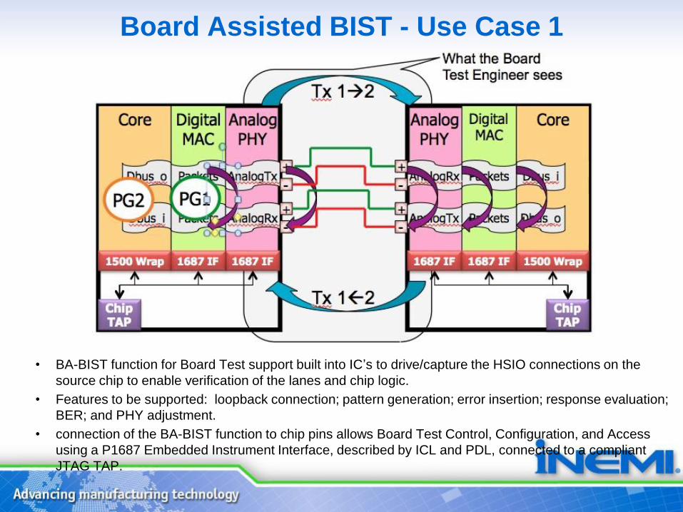
Board Assisted BIST - Use Case 1
• BA-BIST function for Board Test support built into IC’s to drive/capture the HSIO connections on the
source chip to enable verification of the lanes and chip logic.
• Features to be supported: loopback connection; pattern generation; error insertion; response evaluation;
BER; and PHY adjustment.
• connection of the BA-BIST function to chip pins allows Board Test Control, Configuration, and Access
using a P1687 Embedded Instrument Interface, described by ICL and PDL, connected to a compliant
JTAG TAP.
Conclusion
• Testability in memory devices is almost non-existant.
• DFT techniques will be mainsteam, enabling more
solutions to the problem of testing soldered down
memory.
• Board-centric DFT is needed to improve the testability
of nets without testpoint access.
• Board-assist BIST deisgned into integrated circuits can
address this.
– Future steps to support this in the short term are to continue to
educate and influence the industry about board BIST
requirements and in the long term to provide specific BIST
standardization use-case models for HSIO and IC to external
memory to the P1687 standards body for implementation into
the standard.

www.inemi.org
26
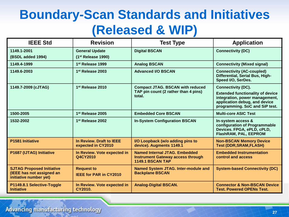
Boundary-Scan Standards and Initiatives
(Released & WIP)
27
IEEE Std Revision Test Type Application
1149.1-2001
(BSDL added 1994)
General Update
(1st Release 1990)
Digital BSCAN Connectivity (DC)
1149.4-1999 1st Release 1999 Analog BSCAN Connectivity (Mixed signal)
1149.6-2003 1st Release 2003 Advanced I/O BSCAN Connectivity (AC-coupled) Differential, Serial Bus, High-Speed I/O, SerDes.
1149.7-2009 (cJTAG) 1st Release 2010 Compact JTAG. BSCAN with reduced TAP pin count (2 rather than 4 pins) total.
Connectivity (DC).
Extended functionality of device integration, power management, application debug, and device programming. SoC and SiP test.
1500-2005 1st Release 2005 Embedded Core BSCAN Multi-core ASIC Test
1532-2002 1st Release 2002 In-System Configuration BSCAN In-system access & configuration of Programmable Devices. FPGA, ePLD, cPLD, FlashRAM, PAL, EEPROM
P1581 Initiative In Review. Draft to IEEE expected in CY2010
I/O Loopback (w/o adding pins to device). Augments 1149.1
Non-BSCAN Memory Device Test (DDR,SRAM,FLASH)
P1687 (IJTAG) Initiative In Review. Vote expected in Q4CY2010
Named Internal JTAG. Embedded Instrument Gateway access through 1149.1 BSCAN TAP
Embedded Instrumentation control and access
SJTAG Proposed Initiative (IEEE has not assigned an initiative number yet)
Request to
IEEE for PAR in CY2010
Named System JTAG. Inter-module and Backplane BSCAN
System-based Connectivity (DC)
P1149.8.1 Selective-Toggle Initiative
In Review. Vote expected in CY2010.
Analog-Digital BSCAN. Connector & Non-BSCAN Device Test. Powered OPENs Test.