
CSS555 Application Circuits - unitech, electronics · CSS555(C) Application Circuits CSS555/CSS555C...
20
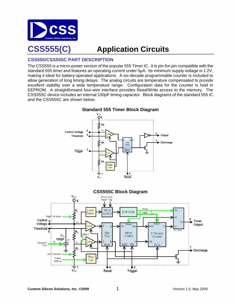
Custom Silicon Solutions, Inc. ©2009 1 Version 1.0, May 2009 css Custom Silicon Solutions, Inc. CSS555(C) Application Circuits CSS555/CSS555C PART DESCRIPTION The CSS555 is a micro-power version of the popular 555 Timer IC. It is pin-for-pin compatible with the standard 555 timer and features an operating current under 5μA. Its minimum supply voltage is 1.2V, making it ideal for battery-operated applications. A six-decade programmable counter is included to allow generation of long timing delays. The analog circuits are temperature compensated to provide excellent stability over a wide temperature range. Configuration data for the counter is held in EEPROM. A straightforward four-wire interface provides Read/Write access to the memory. The CSS555C device includes an internal 100pF timing capacitor. Block diagrams of the standard 555 IC and the CSS555C are shown below. Standard 555 Timer Block Diagram CSS555C Block Diagram
Transcript of CSS555 Application Circuits - unitech, electronics · CSS555(C) Application Circuits CSS555/CSS555C...
Custom Silicon Solutions, Inc. ©2009 1 Version 1.0, May 2009
cssCustom Silicon Solutions, Inc.
CSS555(C) Application Circuits CSS555/CSS555C PART DESCRIPTION The CSS555 is a micro-power version of the popular 555 Timer IC. It is pin-for-pin compatible with the standard 555 timer and features an operating current under 5µA. Its minimum supply voltage is 1.2V, making it ideal for battery-operated applications. A six-decade programmable counter is included to allow generation of long timing delays. The analog circuits are temperature compensated to provide excellent stability over a wide temperature range. Configuration data for the counter is held in EEPROM. A straightforward four-wire interface provides Read/Write access to the memory. The CSS555C device includes an internal 100pF timing capacitor. Block diagrams of the standard 555 IC and the CSS555C are shown below.
Standard 555 Timer Block Diagram
CSS555C Block Diagram
Custom Silicon Solutions, Inc. ©2009 2 Version 1.0, May 2009
CSS555(C) Application Circuits Application Circuits The following 555 timer circuits have been assembled to help show the advantages of the CSS555C timer. Its advanced features offer unique capabilities that can reduce power, decrease PCB area and eliminate the external timing capacitor. These circuits demonstrate many of the basic 555 timer functions. They can also be used as a starting point to improve existing timer circuits or to develop new ones.
Miscellaneous Notes Power Supply Bypassing : The original 555 Timer IC’s were made using a bipolar technology and required significant power supply bypassing (like early digital TTL ICs). Current spikes during output transitions could exceed 250mA. The CSS555C employs a “break-before-make” CMOS output driver that eliminates these spikes. Minimal supply bypassing is therefore required. A 0.001 uF capacitor is usually adequate for most applications. If a large capacitive load needs to be driven by the Timer Output, a larger bypass capacitor may be required. Control Voltage : The Control Voltage input (pin 5) provides access to the upper level trip point. It is derived from a high impedance resistive divider. As with any high impedance node, it should be isolated from sources of DC leakage and high-level clock/data signals that might be capacitively coupled into it. Keep this trace as short as possible. When possible, surround (shield) the Control Voltage signal with an AC ground. In most applications it does not require a bypass capacitor. Stray Capacitance : When using the CSS555C, it is important to minimize the stray capacitance on the Threshold and Discharge pins. The internal timing capacitor is 100pF. Printed circuit boards typically add several picofarads of stray capacitance if the routing is kept as short as possible. Timing resistors RA and RB should be located as close to the IC as possible. The stray capacitance (CSTRAY) will be fairly consistent from board-to-board and can be accounted for when selecting the timing resistors. (The internal timing capacitor can be electronically trimmed to adjust for variations in CSTRAY, RA and RB.) During development, remember that test sockets, proto-boards, connectors and cables can add significant stray capacitance to these nodes. (A typical proto-board adds about 5pF per pin.) In most prototype fixtures, the monostable delay times and astable periods will be longer than expected. After a PCB is built, delay times will approach their expected values.
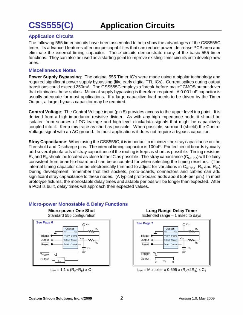
Micro-power Monostable & Delay Functions Micro-power One Shot Long Range Delay Timer Standard 555 configuration Extended range – 1 msec to days tPW = 1.1 x (RA+RB) x CT tPW = Multiplier x 0.695 x (RA+2RB) x CT
VDD
RA
Trigger
Output
Reset CT
VDD
Dischg
Thresh
Control
CSS555 VSS
Trigger
Output
Reset RB
VTH
See Page 6
Trigger
Output tPW
VDD
RA
Trigger
Output
Reset CT
VDD
Dischg
Thresh
Control
CSS555 VSS
Trigger
Output
Reset RB
VTH
See Page 7
Trigger
Output tPW
Custom Silicon Solutions, Inc. ©2009 3 Version 1.0, May 2009
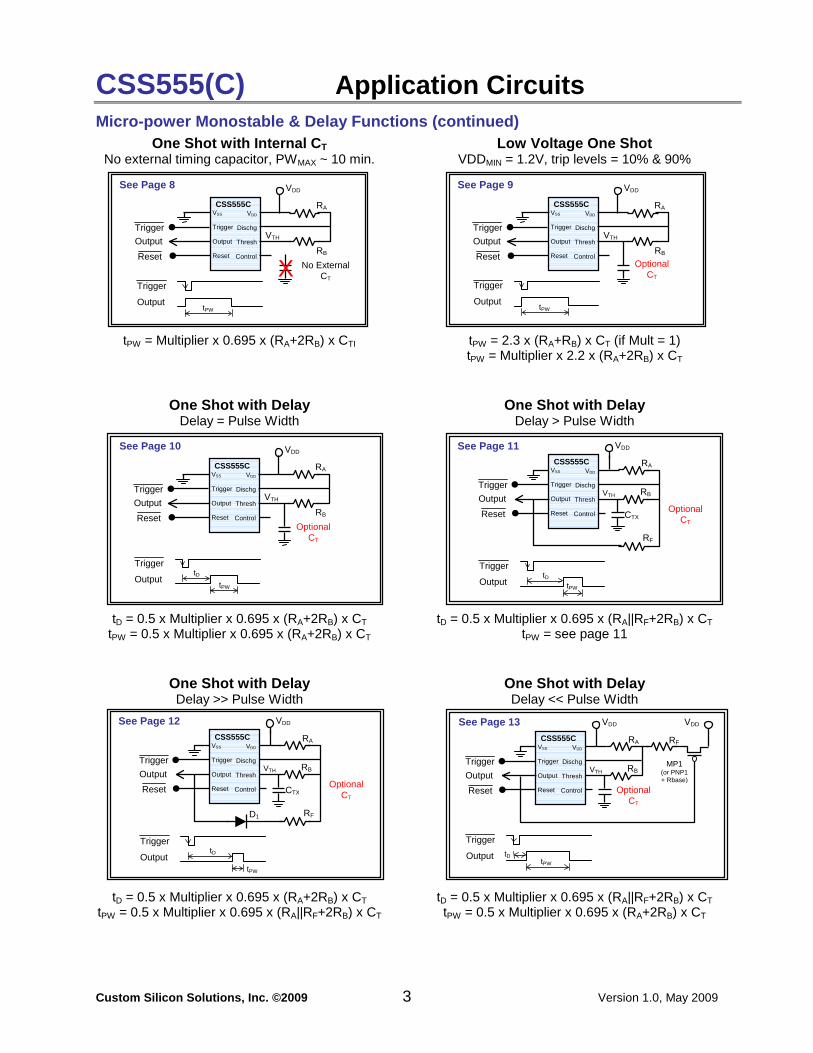
CSS555(C) Application Circuits Micro-power Monostable & Delay Functions (continued ) One Shot with Internal C T Low Voltage One Shot No external timing capacitor, PWMAX ~ 10 min. VDDMIN = 1.2V, trip levels = 10% & 90% tPW = Multiplier x 0.695 x (RA+2RB) x CTI tPW = 2.3 x (RA+RB) x CT (if Mult = 1) tPW = Multiplier x 2.2 x (RA+2RB) x CT One Shot with Delay One Shot with Delay Delay = Pulse Width Delay > Pulse Width tD = 0.5 x Multiplier x 0.695 x (RA+2RB) x CT tD = 0.5 x Multiplier x 0.695 x (RA||RF+2RB) x CT tPW = 0.5 x Multiplier x 0.695 x (RA+2RB) x CT tPW = see page 11 One Shot with Delay One Shot with Delay Delay >> Pulse Width Delay << Pulse Width tD = 0.5 x Multiplier x 0.695 x (RA+2RB) x CT tD = 0.5 x Multiplier x 0.695 x (RA||RF+2RB) x CT tPW = 0.5 x Multiplier x 0.695 x (RA||RF+2RB) x CT tPW = 0.5 x Multiplier x 0.695 x (RA+2RB) x CT
VDD
RA
Trigger
Output
Reset
VDD
Dischg
Thresh
Control
CSS555C VSS
Trigger
Output
Reset RB
VTH
Optional CT
Trigger
Output tPW
tD
See Page 10 VDD
RA
Trigger
Output
Reset CTX
VDD
Dischg
Thresh
Control
CSS555C VSS
Trigger
Output
Reset
RB VTH
RF
Optional CT
Trigger
Output tPW
tD
See Page 11
VDD
RA
Trigger
Output
Reset CTX
VDD
Dischg
Thresh
Control
CSS555C VSS
Trigger
Output
Reset
RB VTH
RF D1
Optional CT
Trigger
Output tPW
tD
See Page 12 VDD
RA
Trigger
Output
Reset
VDD
Dischg
Thresh
Control
CSS555C VSS
Trigger
Output
Reset
RB VTH
RF
MP1 (or PNP1 + Rbase)
VDD
Optional CT
Trigger
Output tPW
tD
See Page 13
VDD
RA
Trigger
Output
Reset
VDD
Dischg
Thresh
Control
CSS555C VSS
Trigger
Output
Reset RB
VTH
No External CT X
Trigger
Output tPW
See Page 8 VDD
RA
Trigger
Output
Reset
VDD
Dischg
Thresh
Control
CSS555C VSS
Trigger
Output
Reset RB
VTH
Optional CT
Trigger
Output tPW
See Page 9
Custom Silicon Solutions, Inc. ©2009 4 Version 1.0, May 2009
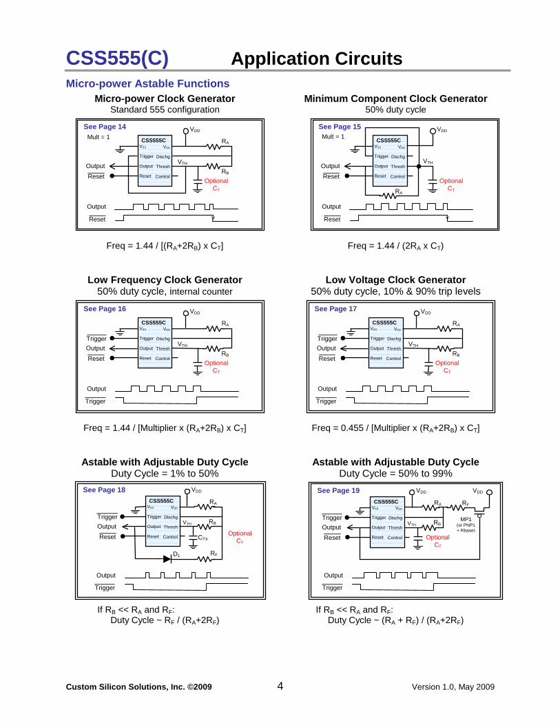
CSS555(C) Application Circuits Micro-power Astable Functions Micro-power Clock Generator Minimum Component Cloc k Generator Standard 555 configuration 50% duty cycle Freq = 1.44 / [(RA+2RB) x CT] Freq = 1.44 / (2RA x CT) Low Frequency Clock Generator Low Voltage Clock Ge nerator 50% duty cycle, internal counter 50% duty cycle, 10% & 90% trip levels Freq = 1.44 / [Multiplier x (RA+2RB) x CT] Freq = 0.455 / [Multiplier x (RA+2RB) x CT] Astable with Adjustable Duty Cycle Astable with Ad justable Duty Cycle Duty Cycle = 1% to 50% Duty Cycle = 50% to 99% If RB << RA and RF: If RB << RA and RF: Duty Cycle ~ RF / (RA+2RF) Duty Cycle ~ (RA + RF) / (RA+2RF)
VDD
RA
Trigger
Output
Reset CTX
VDD
Dischg
Thresh
Control
CSS555C VSS
Trigger
Output
Reset
RB VTH
RF D1
Optional CT
See Page 18
Output
Trigger
VDD
RA
Trigger
Output
Reset
VDD
Dischg
Thresh
Control
CSS555C VSS
Trigger
Output
Reset
RB VTH
RF
MP1 (or PNP1 + Rbase)
VDD
Optional CT
See Page 19
Output
Trigger
VDD
RA
Output
Reset
VDD
Dischg
Thresh
Control
CSS555C VSS
Trigger
Output
Reset
Output
Trigger
RB
VTH
Optional CT
Trigger
See Page 16 VDD
RA
Output
Reset
VDD
Dischg
Thresh
Control
CSS555C VSS
Trigger
Output
Reset
Output
Trigger
RB
VTH
Optional CT
Trigger
See Page 17
VDD
RA
Output
Reset
VDD
Dischg
Thresh
Control
CSS555C VSS
Trigger
Output
Reset
Output
Reset
RB
VTH
Optional CT
See Page 14 Mult = 1
VDD
RA
Output
Reset
VDD
Dischg
Thresh
Control
CSS555C VSS
Trigger
Output
Reset
Output
Reset
VTH
Optional CT
See Page 15 Mult = 1
Custom Silicon Solutions, Inc. ©2009 5 Version 1.0, May 2009
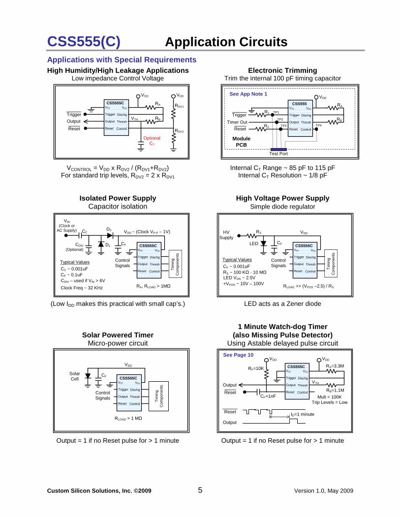
CSS555(C) Application Circuits Applications with Special Requirements High Humidity/High Leakage Applications Electronic Trimming Low impedance Control Voltage Trim the internal 100 pF timing capacitor VCONTROL = VDD x RDV2 / (RDV1+RDV2) Internal CT Range ~ 85 pF to 115 pF For standard trip levels, RDV2 = 2 x RDV1 Internal CT Resolution ~ 1/8 pF Isolated Power Supply High Voltage Power Supply Capacitor isolation Simple diode regulator (Low IDD makes this practical with small cap’s.) LED acts as a Zener diode 1 Minute Watch-dog Timer Solar Powered Timer (also Missing Pulse Detector) Micro-power circuit Using Astable delayed pulse circuit Output = 1 if no Reset pulse for > 1 minute Output = 1 if no Reset pulse for > 1 minute
VDD
RA=3.3M
Output
Reset
VDD
Dischg
Thresh
Control
CSS555C VSS
Trigger
Output
Reset RB=1.1M
VTH
Reset
Output
See Page 10 VDD
CF=1nF
RF=10K
Mult = 100K Trip Levels = Low
tD=1 minute
VDD
CF
VDD
Dischg
Thresh
Control
CSS555C VSS
Trigger
Output
Reset
Tim
ing
Com
pone
nts
Solar Cell
Control Signals
RLOAD > 1 MΩ
VDD
RA
Trigger
Output
Reset
VDD
Dischg
Thresh
Control
CSS555C VSS
Trigger
Output
Reset
RB VTH
Optional CT
VDD
RDV1
RDV2
Trigger
Reset
Timer Out
VDD
Dischg
Thresh
Control
CSS555 VSS
Trigger
Output
Reset
Test Port
Module PCB
RA
RB
VDD
TP1
TP2
TP3 TP4
R1
R2
See App Note 1
VDD HV Supply
CF
VDD
Dischg
Thresh
Control
CSS555C VSS
Trigger
Output
Reset
RS
LED
Control Signals
Typical Values
CF ~ 0.001uF
RS ~ 100 KΩ - 10 MΩ
+VPOS ~ 10V – 100V RLOAD >> (VPOS –2.5) / RS
LED VON ~ 2.5V
Tim
ing
Com
pone
nts
VDD ~ (Clock VP-P – 1V)
VIN (Clock or
AC Supply)
CF
VDD
Dischg
Thresh
Control
CSS555C VSS
Trigger
Output
Reset
D2
Tim
ing
Com
pone
nts
CC
D1
Control Signals
Typical Values
CC ~ 0.001uF
CF ~ 0.1uF
Clock Freq ~ 32 KHz RA, RLOAD > 1MΩ
CDIV(Optional)
CDIV – used if VIN > 6V
Custom Silicon Solutions, Inc. ©2009 6 Version 1.0, May 2009
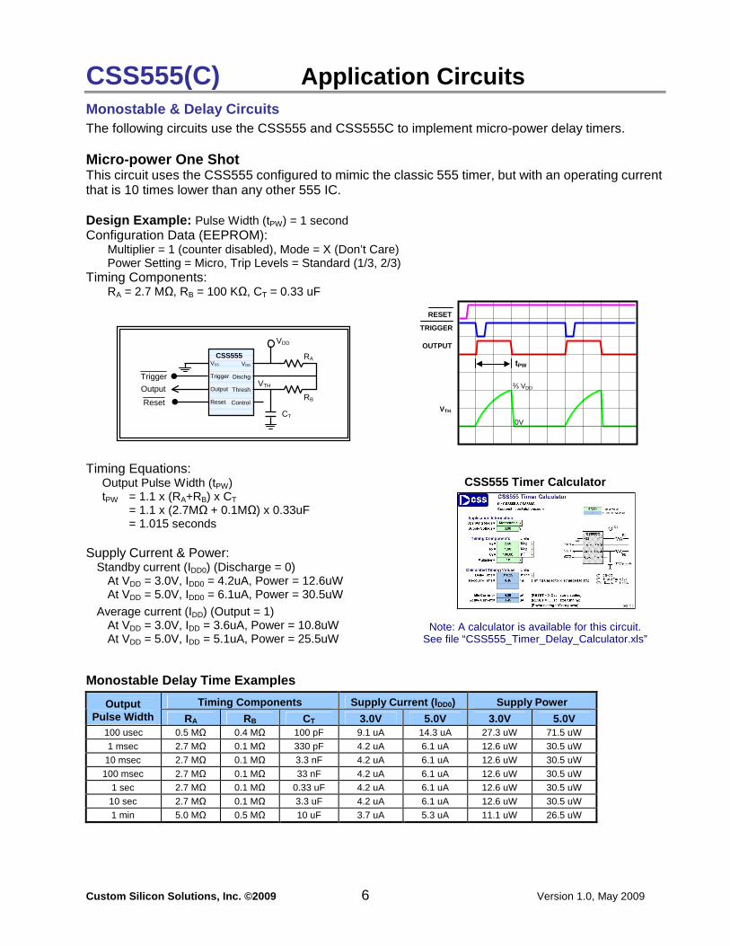
CSS555(C) Application Circuits Monostable & Delay Circuits The following circuits use the CSS555 and CSS555C to implement micro-power delay timers. Micro-power One Shot This circuit uses the CSS555 configured to mimic the classic 555 timer, but with an operating current that is 10 times lower than any other 555 IC. Design Example: Pulse Width (tPW) = 1 second Configuration Data (EEPROM):
Multiplier = 1 (counter disabled), Mode = X (Don’t Care) Power Setting = Micro, Trip Levels = Standard (1/3, 2/3)
Timing Components: RA = 2.7 MΩ, RB = 100 KΩ, CT = 0.33 uF
Timing Equations:
Output Pulse Width (tPW) tPW = 1.1 x (RA+RB) x CT = 1.1 x (2.7MΩ + 0.1MΩ) x 0.33uF = 1.015 seconds
Supply Current & Power:
Standby current (IDD0) (Discharge = 0) At VDD = 3.0V, IDD0 = 4.2uA, Power = 12.6uW At VDD = 5.0V, IDD0 = 6.1uA, Power = 30.5uW
Average current (IDD) (Output = 1) At VDD = 3.0V, IDD = 3.6uA, Power = 10.8uW At VDD = 5.0V, IDD = 5.1uA, Power = 25.5uW
CSS555 Timer Calculator
Note: A calculator is available for this circuit. See file “CSS555_Timer_Delay_Calculator.xls”
Monostable Delay Time Examples
Timing Components Supply Current (I DD0) Supply Power Output Pulse Width RA RB CT 3.0V 5.0V 3.0V 5.0V
100 usec 0.5 MΩ 0.4 MΩ 100 pF 9.1 uA 14.3 uA 27.3 uW 71.5 uW
1 msec 2.7 MΩ 0.1 MΩ 330 pF 4.2 uA 6.1 uA 12.6 uW 30.5 uW
10 msec 2.7 MΩ 0.1 MΩ 3.3 nF 4.2 uA 6.1 uA 12.6 uW 30.5 uW
100 msec 2.7 MΩ 0.1 MΩ 33 nF 4.2 uA 6.1 uA 12.6 uW 30.5 uW
1 sec 2.7 MΩ 0.1 MΩ 0.33 uF 4.2 uA 6.1 uA 12.6 uW 30.5 uW
10 sec 2.7 MΩ 0.1 MΩ 3.3 uF 4.2 uA 6.1 uA 12.6 uW 30.5 uW
1 min 5.0 MΩ 0.5 MΩ 10 uF 3.7 uA 5.3 uA 11.1 uW 26.5 uW
VDD
RA
Trigger
Output
Reset CT
VDD
Dischg
Thresh
Control
CSS555 VSS
Trigger
Output
Reset RB
VTH
TRIGGER
OUTPUT
VTH
0V
⅔ VDD
RESET
tPW
Custom Silicon Solutions, Inc. ©2009 7 Version 1.0, May 2009
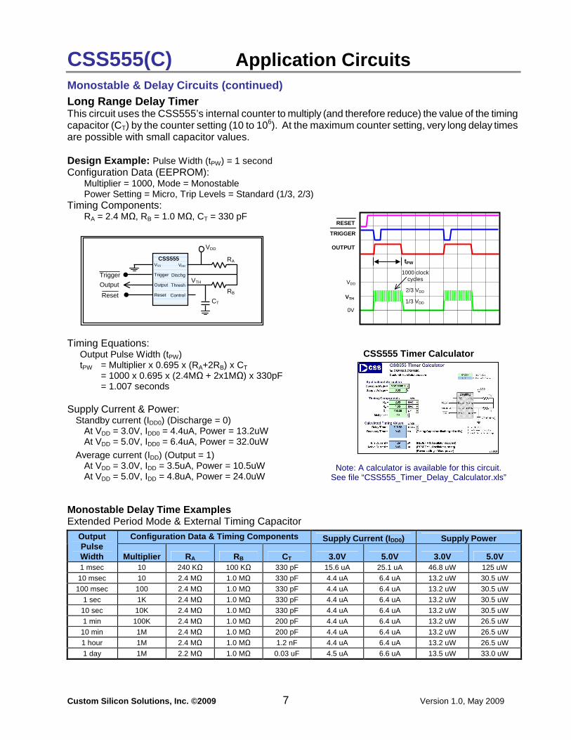
CSS555(C) Application Circuits Monostable & Delay Circuits (continued) Long Range Delay Timer This circuit uses the CSS555’s internal counter to multiply (and therefore reduce) the value of the timing capacitor (CT) by the counter setting (10 to 106). At the maximum counter setting, very long delay times are possible with small capacitor values. Design Example: Pulse Width (tPW) = 1 second Configuration Data (EEPROM):
Multiplier = 1000, Mode = Monostable Power Setting = Micro, Trip Levels = Standard (1/3, 2/3)
Timing Components: RA = 2.4 MΩ, RB = 1.0 MΩ, CT = 330 pF
Timing Equations:
Output Pulse Width (tPW) tPW = Multiplier x 0.695 x (RA+2RB) x CT = 1000 x 0.695 x (2.4MΩ + 2x1MΩ) x 330pF = 1.007 seconds
Supply Current & Power:
Standby current (IDD0) (Discharge = 0) At VDD = 3.0V, IDD0 = 4.4uA, Power = 13.2uW At VDD = 5.0V, IDD0 = 6.4uA, Power = 32.0uW
Average current (IDD) (Output = 1) At VDD = 3.0V, IDD = 3.5uA, Power = 10.5uW At VDD = 5.0V, IDD = 4.8uA, Power = 24.0uW
CSS555 Timer Calculator
Note: A calculator is available for this circuit. See file “CSS555_Timer_Delay_Calculator.xls”
Monostable Delay Time Examples Extended Period Mode & External Timing Capacitor
Configuration Data & Timing Components Supply Current (I DD0) Supply Power Output Pulse Width Multiplier RA RB CT 3.0V 5.0V 3.0V 5.0V 1 msec 10 240 KΩ 100 KΩ 330 pF 15.6 uA 25.1 uA 46.8 uW 125 uW
10 msec 10 2.4 MΩ 1.0 MΩ 330 pF 4.4 uA 6.4 uA 13.2 uW 30.5 uW
100 msec 100 2.4 MΩ 1.0 MΩ 330 pF 4.4 uA 6.4 uA 13.2 uW 30.5 uW
1 sec 1K 2.4 MΩ 1.0 MΩ 330 pF 4.4 uA 6.4 uA 13.2 uW 30.5 uW
10 sec 10K 2.4 MΩ 1.0 MΩ 330 pF 4.4 uA 6.4 uA 13.2 uW 30.5 uW
1 min 100K 2.4 MΩ 1.0 MΩ 200 pF 4.4 uA 6.4 uA 13.2 uW 26.5 uW
10 min 1M 2.4 MΩ 1.0 MΩ 200 pF 4.4 uA 6.4 uA 13.2 uW 26.5 uW
1 hour 1M 2.4 MΩ 1.0 MΩ 1.2 nF 4.4 uA 6.4 uA 13.2 uW 26.5 uW
1 day 1M 2.2 MΩ 1.0 MΩ 0.03 uF 4.5 uA 6.6 uA 13.5 uW 33.0 uW
TRIGGER
OUTPUT
VTH
0V
2/3 VDD
RESET
tPW
1/3 VDD
VDD
1000 clock cycles
VDD
RA
Trigger
Output
Reset
VDD
Dischg
Thresh
Control
CSS555 VSS
Trigger
Output
Reset RB
VTH
CT
Custom Silicon Solutions, Inc. ©2009 8 Version 1.0, May 2009
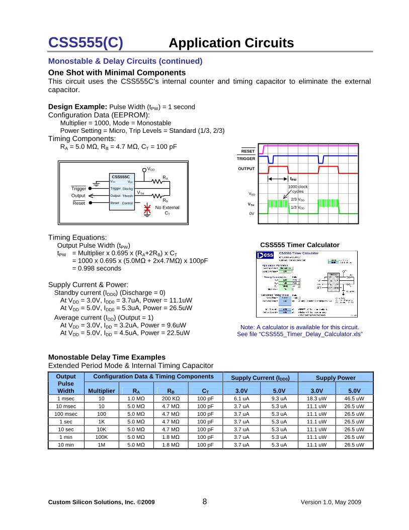
CSS555(C) Application Circuits Monostable & Delay Circuits (continued) One Shot with Minimal Components This circuit uses the CSS555C’s internal counter and timing capacitor to eliminate the external capacitor. Design Example: Pulse Width (tPW) = 1 second Configuration Data (EEPROM):
Multiplier = 1000, Mode = Monostable Power Setting = Micro, Trip Levels = Standard (1/3, 2/3)
Timing Components: RA = 5.0 MΩ, RB = 4.7 MΩ, CT = 100 pF
Timing Equations:
Output Pulse Width (tPW) tPW = Multiplier x 0.695 x (RA+2RB) x CT = 1000 x 0.695 x (5.0MΩ + 2x4.7MΩ) x 100pF = 0.998 seconds
Supply Current & Power:
Standby current (IDD0) (Discharge = 0) At VDD = 3.0V, IDD0 = 3.7uA, Power = 11.1uW At VDD = 5.0V, IDD0 = 5.3uA, Power = 26.5uW
Average current (IDD) (Output = 1) At VDD = 3.0V, IDD = 3.2uA, Power = 9.6uW At VDD = 5.0V, IDD = 4.5uA, Power = 22.5uW
CSS555 Timer Calculator
Note: A calculator is available for this circuit. See file “CSS555_Timer_Delay_Calculator.xls”
Monostable Delay Time Examples Extended Period Mode & Internal Timing Capacitor
Configuration Data & Timing Components Supply Current (I DD0) Supply Power Output Pulse Width Multiplier RA RB CT 3.0V 5.0V 3.0V 5.0V 1 msec 10 1.0 MΩ 200 KΩ 100 pF 6.1 uA 9.3 uA 18.3 uW 46.5 uW
10 msec 10 5.0 MΩ 4.7 MΩ 100 pF 3.7 uA 5.3 uA 11.1 uW 26.5 uW
100 msec 100 5.0 MΩ 4.7 MΩ 100 pF 3.7 uA 5.3 uA 11.1 uW 26.5 uW
1 sec 1K 5.0 MΩ 4.7 MΩ 100 pF 3.7 uA 5.3 uA 11.1 uW 26.5 uW
10 sec 10K 5.0 MΩ 4.7 MΩ 100 pF 3.7 uA 5.3 uA 11.1 uW 26.5 uW
1 min 100K 5.0 MΩ 1.8 MΩ 100 pF 3.7 uA 5.3 uA 11.1 uW 26.5 uW
10 min 1M 5.0 MΩ 1.8 MΩ 100 pF 3.7 uA 5.3 uA 11.1 uW 26.5 uW
VDD
RA
Trigger
Output
Reset
VDD
Dischg
Thresh
Control
CSS555C VSS
Trigger
Output
Reset RB
VTH
No External CT X
TRIGGER
OUTPUT
VTH
0V
2/3 VDD
RESET
tPW
1/3 VDD
VDD
1000 clock cycles

Custom Silicon Solutions, Inc. ©2009 9 Version 1.0, May 2009
CSS555(C) Application Circuits Monostable & Delay Circuits (continued) Low Voltage One Shot The trip levels are configured for 10% and 90% of VDD, allowing operation down to 1.2V. These trip levels may be used with or without the internal counter and timing capacitor. Design Example: Pulse Width (tPW) = 1 second Configuration Data (EEPROM):
Multiplier = 1000, Mode = Monostable Power Setting = Micro, Trip Levels = Low VDD (10%, 90%)
Timing Components: RA = 2.6 MΩ, RB = 1.0 MΩ, CT = 100 pF
Timing Equations:
Output Pulse Width (tPW) tPW = Multiplier x 2.197 x (RA+2RB) x CT = 1000 x 2.197 x (2.6MΩ + 2x1.0MΩ) x 100pF = 1.01 seconds
Supply Current & Power:
Standby current (IDD0) (Discharge = 0) At VDD = 1.5V, IDD0 = 2.8uA, Power = 4.2uW At VDD = 3.0V, IDD0 = 4.3uA, Power = 12.9uW
Average current (IDD) (Output = 1) At VDD = 1.5V, IDD = 2.4uA, Power = 7.2uW At VDD = 3.0V, IDD = 3.5uA, Power = 10.5uW
CSS555 Timer Calculator
Note: A calculator is available for this circuit. See file “CSS555_Timer_Delay_Calculator.xls”
Monostable Delay Time Examples Low VDD Configuration (Trip levels = 10% & 90%)
Configuration Data & Timing Components Supply Current (I DD0) Supply Power Output Pulse Width Multiplier RA RB CT 1.5V 3.0V 1.5V 3.0V 1 msec 1 3.3 MΩ 1.0 MΩ 100 pF 2.7 uA 4.0 uA 4.1 uW 12.2 uW
10 msec 10 2.6 MΩ 1.0 MΩ 100 pF 2.8 uA 4.3 uA 4.2 uW 12.9 uW
100 msec 100 2.6 MΩ 1.0 MΩ 100 pF 2.8 uA 4.3 uA 4.2 uW 12.9 uW
1 sec 1K 2.6 MΩ 1.0 MΩ 100 pF 2.8 uA 4.3 uA 4.2 uW 12.9 uW
10 sec 10K 2.6 MΩ 1.0 MΩ 100 pF 2.8 uA 4.3 uA 4.2 uW 12.9 uW
1 min 100K 2.6 MΩ 1.0 MΩ 100 pF 2.8 uA 4.3 uA 4.2 uW 12.9 uW
10 min 1M 2.6 MΩ 1.0 MΩ 100 pF 2.8 uA 4.3 uA 4.2 uW 12.9 uW
VDD
RA
Trigger
Output
Reset
VDD
Dischg
Thresh
Control
CSS555C VSS
Trigger
Output
Reset RB
VTH
Optional CT
TRIGGER
OUTPUT
VTH
0V
90% VDD
RESET
tPW
10% VDD
VDD
1000 clock cycles
Custom Silicon Solutions, Inc. ©2009 10 Version 1.0, May 2009
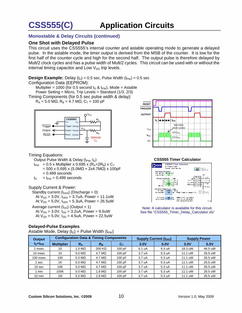
CSS555(C) Application Circuits Monostable & Delay Circuits (continued) One Shot with Delayed Pulse This circuit uses the CSS555’s internal counter and astable operating mode to generate a delayed pulse. In the astable mode, the timer output is derived from the MSB of the counter. It is low for the first half of the counter cycle and high for the second half. The output pulse is therefore delayed by Mult/2 clock cycles and has a pulse width of Mult/2 cycles. This circuit can be used with or without the internal timing capacitor and Low VDD trip levels. Design Example: Delay (tD) = 0.5 sec, Pulse Width (tPW) = 0.5 sec Configuration Data (EEPROM):
Multiplier = 1000 (for 0.5 second tD & tPW), Mode = Astable Power Setting = Micro, Trip Levels = Standard (1/3, 2/3)
Timing Components (for 0.5 sec pulse width & delay): RA = 5.0 MΩ, RB = 4.7 MΩ, CT = 100 pF
Timing Equations:
Output Pulse Width & Delay (tPW, tD) tPW = 0.5 x Multiplier x 0.695 x (RA+2RB) x CT = 500 x 0.695 x (5.0MΩ + 2x4.7MΩ) x 100pF = 0.499 seconds tD = tPW = 0.499 seconds
Supply Current & Power:
Standby current (IDD0) (Discharge = 0) At VDD = 3.0V, IDD0 = 3.7uA, Power = 11.1uW At VDD = 5.0V, IDD0 = 5.3uA, Power = 26.5uW
Average current (IDD) (Output = 1) At VDD = 3.0V, IDD = 3.2uA, Power = 9.6uW At VDD = 5.0V, IDD = 4.5uA, Power = 22.5uW
CSS555 Timer Calculator
Note: A calculator is available for this circuit. See file “CSS555_Timer_Delay_Calculator.xls”
Delayed-Pulse Examples Astable Mode, Delay (tD) = Pulse Width (tPW)
Configuration Data & Timing Components Supply Current (I DD0) Supply Power Output tD+tPW Multiplier RA RB CT 3.0V 5.0V 3.0V 5.0V 1 msec 10 1.0 MΩ 200 KΩ 100 pF 6.1 uA 9.3 uA 18.3 uW 46.5 uW
10 msec 10 5.0 MΩ 4.7 MΩ 100 pF 3.7 uA 5.3 uA 11.1 uW 26.5 uW
100 msec 100 5.0 MΩ 4.7 MΩ 100 pF 3.7 uA 5.3 uA 11.1 uW 26.5 uW
1 sec 1K 5.0 MΩ 4.7 MΩ 100 pF 3.7 uA 5.3 uA 11.1 uW 26.5 uW
10 sec 10K 5.0 MΩ 4.7 MΩ 100 pF 3.7 uA 5.3 uA 11.1 uW 26.5 uW
1 min 100K 5.0 MΩ 1.8 MΩ 100 pF 3.7 uA 5.3 uA 11.1 uW 26.5 uW
10 min 1M 5.0 MΩ 1.8 MΩ 100 pF 3.7 uA 5.3 uA 11.1 uW 26.5 uW
VDD
RA
Trigger
Output
Reset
VDD
Dischg
Thresh
Control
CSS555C VSS
Trigger
Output
Reset RB
VTH
Optional CT
TRIGGER
OUTPUT
VTH
0V
2/3 VDD
RESET
tPW
1/3 VDD
VDD
500+500 clock cycles
tD
Custom Silicon Solutions, Inc. ©2009 11 Version 1.0, May 2009
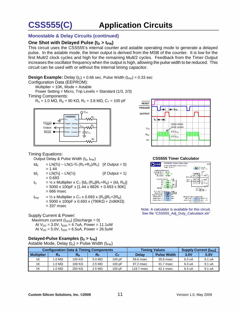
CSS555(C) Application Circuits Monostable & Delay Circuits (continued) One Shot with Delayed Pulse (t D > tPW) This circuit uses the CSS555’s internal counter and astable operating mode to generate a delayed pulse. In the astable mode, the timer output is derived from the MSB of the counter. It is low for the first Mult/2 clock cycles and high for the remaining Mult/2 cycles. Feedback from the Timer Output increases the oscillator frequency when the output is high, allowing the pulse width to be reduced. This circuit can be used with or without the internal timing capacitor. Design Example: Delay (tD) = 0.66 sec, Pulse Width (tPW) = 0.33 sec Configuration Data (EEPROM):
Multiplier = 10K, Mode = Astable Power Setting = Micro, Trip Levels = Standard (1/3, 2/3)
Timing Components: RA = 1.0 MΩ, RB = 90 KΩ, RF = 3.8 MΩ, CT = 100 pF
Timing Equations:
Output Delay & Pulse Width (tD, tPW)
td0 = LN(⅔) – LN(1-⅔ (RF+RA)/RF) (if Output = 0) = 1.44 td1 = LN(⅔) – LN(⅓) (if Output = 1) = 0.693 tD = ½ x Multiplier x CT [td0 (RA||RF+RB) + (td1 RB)] = 5000 x 100pF x [1.44 x 882K + 0.693 x 90K] = 666 msec
tPW = ½ x Multiplier x CT x 0.693 x (RA||RF+2RB) = 5000 x 100pF x 0.693 x (790KΩ + 2x90KΩ) = 337 msec
Supply Current & Power:
Maximum current (IDD0) (Discharge = 0) At VDD = 3.0V, IDD0 = 4.7uA, Power = 11.1uW At VDD = 5.0V, IDD0 = 6.5uA, Power = 26.5uW
CSS555 Timer Calculator
Note: A calculator is available for this circuit. See file “CSS555_Adj_Duty_Calculator.xls”
Delayed-Pulse Examples (t D > tPW) Astable Mode, Delay (tD) > Pulse Width (tPW)
Configuration Data & Timing Components Timing Values Supply Current (I DD0) Multiplier RA RB RF CT Delay Pulse Width 3.0V 5.0V
1K 1.0 MΩ 100 KΩ 5.0 MΩ 100 pF 59.6 msec 35.8 msec 6.3 uA 9.1 uA
1K 1.0 MΩ 100 KΩ 2.5 MΩ 100 pF 97.2 msec 31.7 msec 6.3 uA 9.1 uA
1K 1.0 MΩ 250 KΩ 2.5 MΩ 100 pF 119.7 msec 42.1 msec 6.3 uA 9.1 uA
VDD
RA
Trigger
Output
Reset CTX
VDD
Dischg
Thresh
Control
CSS555C VSS
Trigger
Output
Reset
RB VTH
RF
TRIGGER
OUTPUT
VTH
0V
2/3 VDD
RESET
tPW
1/3 VDD
VDD
5000+5000 clock cycles
tD
Custom Silicon Solutions, Inc. ©2009 12 Version 1.0, May 2009
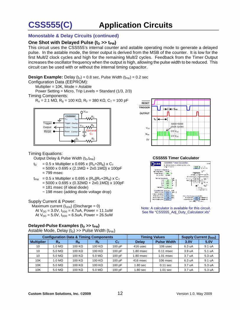
CSS555(C) Application Circuits Monostable & Delay Circuits (continued) One Shot with Delayed Pulse (t D >> tPW) This circuit uses the CSS555’s internal counter and astable operating mode to generate a delayed pulse. In the astable mode, the timer output is derived from the MSB of the counter. It is low for the first Mult/2 clock cycles and high for the remaining Mult/2 cycles. Feedback from the Timer Output increases the oscillator frequency when the output is high, allowing the pulse width to be reduced. This circuit can be used with or without the internal timing capacitor. Design Example: Delay (tD) = 0.8 sec, Pulse Width (tPW) = 0.2 sec Configuration Data (EEPROM):
Multiplier = 10K, Mode = Astable Power Setting = Micro, Trip Levels = Standard (1/3, 2/3)
Timing Components: RA = 2.1 MΩ, RB = 100 KΩ, RF = 380 KΩ, CT = 100 pF
Timing Equations:
Output Delay & Pulse Width (tD,tPW)
tD = 0.5 x Multiplier x 0.695 x (RA+2RB) x CT = 5000 x 0.695 x (2.1MΩ + 2x0.1MΩ) x 100pF = 799 msec
tPW = 0.5 x Multiplier x 0.695 x (RA||RF+2RB) x CT = 5000 x 0.695 x (0.32MΩ + 2x0.1MΩ) x 100pF = 181 msec (if ideal diode) ~ 198 msec (adding diode voltage drop)
Supply Current & Power:
Maximum current (IDD0) (Discharge = 0) At VDD = 3.0V, IDD0 = 4.7uA, Power = 11.1uW At VDD = 5.0V, IDD0 = 6.5uA, Power = 26.5uW
CSS555 Timer Calculator
Note: A calculator is available for this circuit. See file “CSS555_Adj_Duty_Calculator.xls”
Delayed-Pulse Examples (t D >> tPW) Astable Mode, Delay (tD) >> Pulse Width (tPW)
Configuration Data & Timing Components Timing Values Supply Current (I DD0) Multiplier RA RB RF CT Delay Pulse Width 3.0V 5.0V
10 1.0 MΩ 100 KΩ 100 KΩ 100 pF 416 usec 106 usec 6.3 uA 9.1 uA
10 5.0 MΩ 100 KΩ 100 KΩ 100 pF 1.80 msec 0.11 msec 3.9 uA 5.1 uA
10 5.0 MΩ 100 KΩ 5.0 MΩ 100 pF 1.80 msec 1.01 msec 3.7 uA 5.3 uA
10K 1.0 MΩ 100 KΩ 100 KΩ 100 pF 416 msec 106 msec 6.3 uA 9.1 uA
10K 5.0 MΩ 100 KΩ 100 KΩ 100 pF 1.80 sec 0.11 sec 3.7 uA 5.3 uA
10K 5.0 MΩ 100 KΩ 5.0 MΩ 100 pF 1.80 sec 1.01 sec 3.7 uA 5.3 uA
TRIGGER
OUTPUT
VTH
0V
2/3 VDD
RESET
tPW
1/3 VDD
VDD
5000+5000 clock cycles
tD
VDD
RA
Trigger
Output
Reset
VDD
Dischg
Thresh
Control
CSS555C VSS
Trigger
Output
Reset
RB VTH
RF D1
Optional CT
Custom Silicon Solutions, Inc. ©2009 13 Version 1.0, May 2009
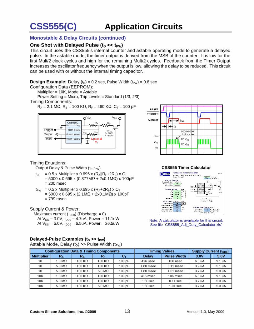
CSS555(C) Application Circuits Monostable & Delay Circuits (continued) One Shot with Delayed Pulse (t D << tPW) This circuit uses the CSS555’s internal counter and astable operating mode to generate a delayed pulse. In the astable mode, the timer output is derived from the MSB of the counter. It is low for the first Mult/2 clock cycles and high for the remaining Mult/2 cycles. Feedback from the Timer Output increases the oscillator frequency when the output is low, allowing the delay to be reduced. This circuit can be used with or without the internal timing capacitor. Design Example: Delay (tD) = 0.2 sec, Pulse Width (tPW) = 0.8 sec Configuration Data (EEPROM):
Multiplier = 10K, Mode = Astable Power Setting = Micro, Trip Levels = Standard (1/3, 2/3)
Timing Components: RA = 2.1 MΩ, RB = 100 KΩ, RF = 460 KΩ, CT = 100 pF
Timing Equations:
Output Delay & Pulse Width (tD,tPW)
tD = 0.5 x Multiplier x 0.695 x (RA||RF+2RB) x CT = 5000 x 0.695 x (0.377MΩ + 2x0.1MΩ) x 100pF = 200 msec
tPW = 0.5 x Multiplier x 0.695 x (RA+2RB) x CT = 5000 x 0.695 x (2.1MΩ + 2x0.1MΩ) x 100pF = 799 msec
Supply Current & Power:
Maximum current (IDD0) (Discharge = 0) At VDD = 3.0V, IDD0 = 4.7uA, Power = 11.1uW At VDD = 5.0V, IDD0 = 6.5uA, Power = 26.5uW
CSS555 Timer Calculator
Note: A calculator is available for this circuit. See file “CSS555_Adj_Duty_Calculator.xls”
Delayed-Pulse Examples (t D >> tPW) Astable Mode, Delay (tD) >> Pulse Width (tPW)
Configuration Data & Timing Components Timing Values Supply Current (I DD0) Multiplier RA RB RF CT Delay Pulse Width 3.0V 5.0V
10 1.0 MΩ 100 KΩ 100 KΩ 100 pF 416 usec 106 usec 6.3 uA 9.1 uA
10 5.0 MΩ 100 KΩ 100 KΩ 100 pF 1.80 msec 0.11 msec 3.9 uA 5.1 uA
10 5.0 MΩ 100 KΩ 5.0 MΩ 100 pF 1.80 msec 1.01 msec 3.7 uA 5.3 uA
10K 1.0 MΩ 100 KΩ 100 KΩ 100 pF 416 msec 106 msec 6.3 uA 9.1 uA
10K 5.0 MΩ 100 KΩ 100 KΩ 100 pF 1.80 sec 0.11 sec 3.7 uA 5.3 uA
10K 5.0 MΩ 100 KΩ 5.0 MΩ 100 pF 1.80 sec 1.01 sec 3.7 uA 5.3 uA
VDD
RA
Trigger
Output
Reset
VDD
Dischg
Thresh
Control
CSS555C VSS
Trigger
Output
Reset
RB VTH
RF
MP1 (or PNP1 + Rbase)
VDD
Optional CT
TRIGGER
OUTPUT
VTH
0V
2/3 VDD
RESET
tPW
1/3 VDD
VDD
5000+5000 clock cycles
tD
Custom Silicon Solutions, Inc. ©2009 14 Version 1.0, May 2009
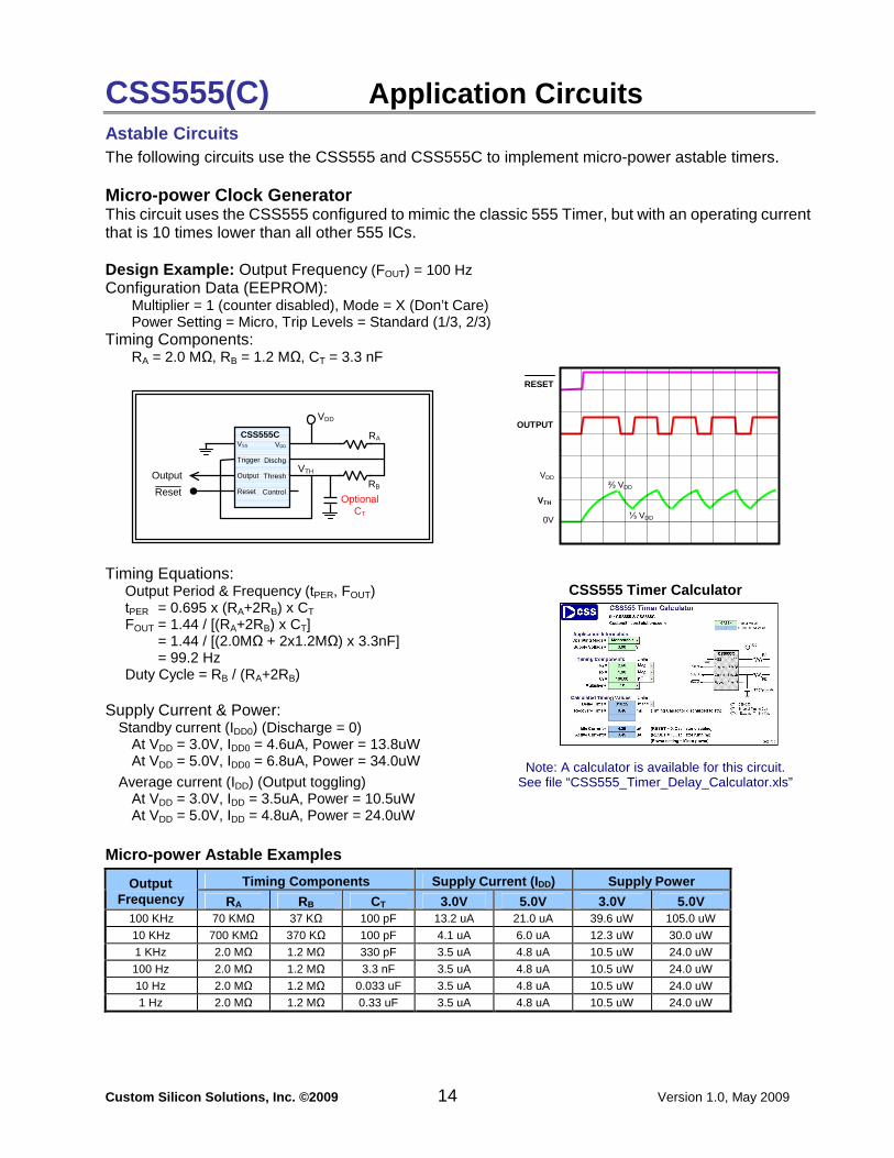
CSS555(C) Application Circuits Astable Circuits The following circuits use the CSS555 and CSS555C to implement micro-power astable timers. Micro-power Clock Generator This circuit uses the CSS555 configured to mimic the classic 555 Timer, but with an operating current that is 10 times lower than all other 555 ICs. Design Example: Output Frequency (FOUT) = 100 Hz Configuration Data (EEPROM):
Multiplier = 1 (counter disabled), Mode = X (Don’t Care) Power Setting = Micro, Trip Levels = Standard (1/3, 2/3)
Timing Components: RA = 2.0 MΩ, RB = 1.2 MΩ, CT = 3.3 nF
Timing Equations:
Output Period & Frequency (tPER, FOUT) tPER = 0.695 x (RA+2RB) x CT FOUT = 1.44 / [(RA+2RB) x CT] = 1.44 / [(2.0MΩ + 2x1.2MΩ) x 3.3nF] = 99.2 Hz Duty Cycle = RB / (RA+2RB)
Supply Current & Power:
Standby current (IDD0) (Discharge = 0) At VDD = 3.0V, IDD0 = 4.6uA, Power = 13.8uW At VDD = 5.0V, IDD0 = 6.8uA, Power = 34.0uW
Average current (IDD) (Output toggling) At VDD = 3.0V, IDD = 3.5uA, Power = 10.5uW At VDD = 5.0V, IDD = 4.8uA, Power = 24.0uW
CSS555 Timer Calculator
Note: A calculator is available for this circuit. See file “CSS555_Timer_Delay_Calculator.xls”
Micro-power Astable Examples
Timing Components Supply Current (I DD) Supply Power Output Frequency RA RB CT 3.0V 5.0V 3.0V 5.0V
100 KHz 70 KMΩ 37 KΩ 100 pF 13.2 uA 21.0 uA 39.6 uW 105.0 uW
10 KHz 700 KMΩ 370 KΩ 100 pF 4.1 uA 6.0 uA 12.3 uW 30.0 uW
1 KHz 2.0 MΩ 1.2 MΩ 330 pF 3.5 uA 4.8 uA 10.5 uW 24.0 uW
100 Hz 2.0 MΩ 1.2 MΩ 3.3 nF 3.5 uA 4.8 uA 10.5 uW 24.0 uW
10 Hz 2.0 MΩ 1.2 MΩ 0.033 uF 3.5 uA 4.8 uA 10.5 uW 24.0 uW
1 Hz 2.0 MΩ 1.2 MΩ 0.33 uF 3.5 uA 4.8 uA 10.5 uW 24.0 uW
VDD
RA
Output
Reset
VDD
Dischg
Thresh
Control
CSS555C VSS
Trigger
Output
Reset RB
VTH
Optional CT
OUTPUT
VTH
0V
⅔ VDD
⅓ VDD
RESET
VDD
Custom Silicon Solutions, Inc. ©2009 15 Version 1.0, May 2009
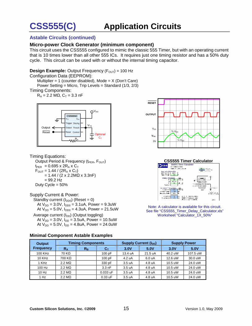
CSS555(C) Application Circuits Astable Circuits (continued) Micro-power Clock Generator (minimum component) This circuit uses the CSS555 configured to mimic the classic 555 Timer, but with an operating current that is 10 times lower than all other 555 ICs. It requires just one timing resistor and has a 50% duty cycle. This circuit can be used with or without the internal timing capacitor. Design Example: Output Frequency (FOUT) = 100 Hz Configuration Data (EEPROM):
Multiplier = 1 (counter disabled), Mode = X (Don’t Care) Power Setting = Micro, Trip Levels = Standard (1/3, 2/3)
Timing Components: RA = 2.2 MΩ, CT = 3.3 nF
Timing Equations:
Output Period & Frequency (tPER, FOUT) tPER = 0.695 x 2RA x CT FOUT = 1.44 / (2RA x CT) = 1.44 / (2 x 2.2MΩ x 3.3nF) = 99.2 Hz Duty Cycle = 50%
Supply Current & Power:
Standby current (IDD0) (Reset = 0) At VDD = 3.0V, IDD0 = 3.1uA, Power = 9.3uW At VDD = 5.0V, IDD0 = 4.3uA, Power = 21.5uW
Average current (IDD) (Output toggling) At VDD = 3.0V, IDD = 3.5uA, Power = 10.5uW At VDD = 5.0V, IDD = 4.8uA, Power = 24.0uW
CSS555 Timer Calculator
Note: A calculator is available for this circuit. See file “CSS555_Timer_Delay_Calculator.xls”
Worksheet “Calculator_1X_50%”
Minimal Component Astable Examples
Timing Components Supply Current (I DD) Supply Power Output Frequency RA RB CT 3.0V 5.0V 3.0V 5.0V
100 KHz 70 KΩ 100 pF 13.4 uA 21.5 uA 40.2 uW 107.5 uW
10 KHz 700 KΩ 100 pF 4.2 uA 6.0 uA 12.6 uW 30.0 uW
1 KHz 2.2 MΩ 330 pF 3.5 uA 4.8 uA 10.5 uW 24.0 uW
100 Hz 2.2 MΩ 3.3 nF 3.5 uA 4.8 uA 10.5 uW 24.0 uW
10 Hz 2.2 MΩ 0.033 uF 3.5 uA 4.8 uA 10.5 uW 24.0 uW
1 Hz 2.2 MΩ 0.33 uF 3.5 uA 4.8 uA 10.5 uW 24.0 uW
VDD
RA
Output
Reset
VDD
Dischg
Thresh
Control
CSS555C VSS
Trigger
Output
Reset
VTH
Optional CT
OUTPUT
VTH
0V
⅔ VDD
⅓ VDD
RESET
VDD
Custom Silicon Solutions, Inc. ©2009 16 Version 1.0, May 2009
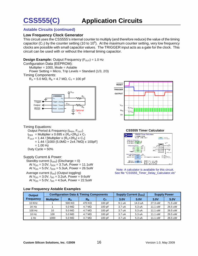
CSS555(C) Application Circuits Astable Circuits (continued) Low Frequency Clock Generator This circuit uses the CSS555’s internal counter to multiply (and therefore reduce) the value of the timing capacitor (CT) by the counter setting (10 to 106). At the maximum counter setting, very low frequency clocks are possible with small capacitor values. The TRIGGER input acts as a gate for the clock. This circuit can be used with or without the internal timing capacitor. Design Example: Output Frequency (FOUT) = 1.0 Hz Configuration Data (EEPROM):
Multiplier = 1000, Mode = Astable Power Setting = Micro, Trip Levels = Standard (1/3, 2/3)
Timing Components: RA = 5.0 MΩ, RB = 4.7 MΩ, CT = 100 pF
Timing Equations:
Output Period & Frequency (tPER, FOUT) tPER = Multiplier x 0.695 x (RA+2RB) x CT FOUT = 1.44 / [Multiplier x (RA+2RB) x CT] = 1.44 / [1000 (5.0MΩ + 2x4.7MΩ) x 100pF] = 1.00 Hz Duty Cycle = 50%
Supply Current & Power:
Standby current (IDD0) (Discharge = 0) At VDD = 3.0V, IDD0 = 3.7uA, Power = 11.1uW At VDD = 5.0V, IDD0 = 5.3uA, Power = 26.5uW
Average current (IDD) (Output toggling) At VDD = 3.0V, IDD = 3.2uA, Power = 9.6uW At VDD = 5.0V, IDD = 4.5uA, Power = 22.5uW
CSS555 Timer Calculator
Note: A calculator is available for this circuit. See file “CSS555_Timer_Delay_Calculator.xls”
Low Frequency Astable Examples
Configuration Data & Timing Components Supply Current (I DD0) Supply Power Output Frequency Multiplier RA RB CT 3.0V 5.0V 3.0V 5.0V
10 KHz 1 500 KΩ 470 KΩ 100 pF 9.1 uA 14.3 uA 27.3 uW 71.5 uW
1K Hz 1 5.0 MΩ 4.7 MΩ 100 pF 3.7 uA 5.3 uA 11.1 uW 26.5 uW
100 Hz 10 5.0 MΩ 4.7 MΩ 100 pF 3.7 uA 5.3 uA 11.1 uW 26.5 uW
10 Hz 100 5.0 MΩ 4.7 MΩ 100 pF 3.7 uA 5.3 uA 11.1 uW 26.5 uW
1 Hz 1000 5.0 MΩ 4.7 MΩ 100 pF 3.7 uA 5.3 uA 11.1 uW 26.5 uW
TRIGGER
OUTPUT
VTH
0V
⅔ VDD
⅓ VDD
RESET
VDD
VDD
RA
Output
Reset
VDD
Dischg
Thresh
Control
CSS555C VSS
Trigger
Output
Reset RB
VTH
Optional CT
Trigger
Custom Silicon Solutions, Inc. ©2009 17 Version 1.0, May 2009
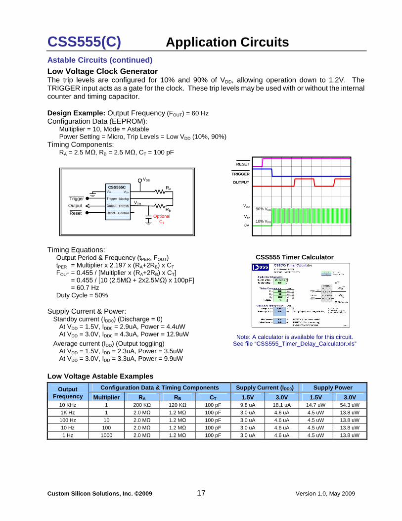
CSS555(C) Application Circuits Astable Circuits (continued) Low Voltage Clock Generator The trip levels are configured for 10% and 90% of VDD, allowing operation down to 1.2V. The TRIGGER input acts as a gate for the clock. These trip levels may be used with or without the internal counter and timing capacitor. Design Example: Output Frequency (FOUT) = 60 Hz Configuration Data (EEPROM):
Multiplier = 10, Mode = Astable Power Setting = Micro, Trip Levels = Low VDD (10%, 90%)
Timing Components: RA = 2.5 MΩ, RB = 2.5 MΩ, CT = 100 pF
Timing Equations:
Output Period & Frequency (tPER, FOUT) tPER = Multiplier x 2.197 x (RA+2RB) x CT FOUT = 0.455 / [Multiplier x (RA+2RB) x CT] = 0.455 / [10 (2.5MΩ + 2x2.5MΩ) x 100pF] = 60.7 Hz Duty Cycle = 50%
Supply Current & Power:
Standby current (IDD0) (Discharge = 0) At VDD = 1.5V, IDD0 = 2.9uA, Power = 4.4uW At VDD = 3.0V, IDD0 = 4.3uA, Power = 12.9uW
Average current (IDD) (Output toggling) At VDD = 1.5V, IDD = 2.3uA, Power = 3.5uW At VDD = 3.0V, IDD = 3.3uA, Power = 9.9uW
CSS555 Timer Calculator
Note: A calculator is available for this circuit. See file “CSS555_Timer_Delay_Calculator.xls”
Low Voltage Astable Examples
Configuration Data & Timing Components Supply Current (I DD0) Supply Power Output Frequency Multiplier RA RB CT 1.5V 3.0V 1.5V 3.0V
10 KHz 1 200 KΩ 120 KΩ 100 pF 9.8 uA 18.1 uA 14.7 uW 54.3 uW
1K Hz 1 2.0 MΩ 1.2 MΩ 100 pF 3.0 uA 4.6 uA 4.5 uW 13.8 uW
100 Hz 10 2.0 MΩ 1.2 MΩ 100 pF 3.0 uA 4.6 uA 4.5 uW 13.8 uW
10 Hz 100 2.0 MΩ 1.2 MΩ 100 pF 3.0 uA 4.6 uA 4.5 uW 13.8 uW
1 Hz 1000 2.0 MΩ 1.2 MΩ 100 pF 3.0 uA 4.6 uA 4.5 uW 13.8 uW
TRIGGER
OUTPUT
VTH
0V
90% VDD
10% VDD
RESET
VDD
VDD
RA
Output
Reset
VDD
Dischg
Thresh
Control
CSS555C VSS
Trigger
Output
Reset RB
VTH
Optional CT
Trigger
Custom Silicon Solutions, Inc. ©2009 18 Version 1.0, May 2009
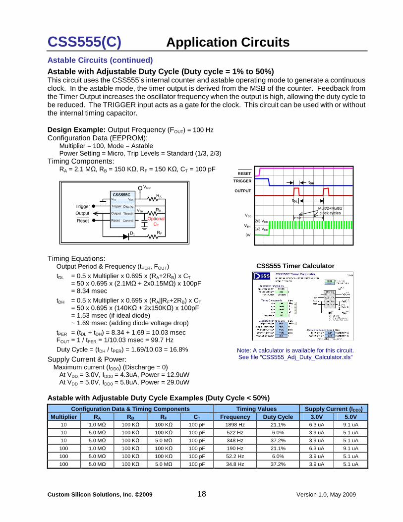
CSS555(C) Application Circuits Astable Circuits (continued) Astable with Adjustable Duty Cycle (Duty cycle = 1% to 50%) This circuit uses the CSS555’s internal counter and astable operating mode to generate a continuous clock. In the astable mode, the timer output is derived from the MSB of the counter. Feedback from the Timer Output increases the oscillator frequency when the output is high, allowing the duty cycle to be reduced. The TRIGGER input acts as a gate for the clock. This circuit can be used with or without the internal timing capacitor. Design Example: Output Frequency (FOUT) = 100 Hz Configuration Data (EEPROM):
Multiplier = 100, Mode = Astable Power Setting = Micro, Trip Levels = Standard (1/3, 2/3)
Timing Components: RA = 2.1 MΩ, RB = 150 KΩ, RF = 150 KΩ, CT = 100 pF
Timing Equations:
Output Period & Frequency (tPER, FOUT)
tDL = 0.5 x Multiplier x 0.695 x (RA+2RB) x CT = 50 x 0.695 x (2.1MΩ + 2x0.15MΩ) x 100pF = 8.34 msec
tDH = 0.5 x Multiplier x 0.695 x (RA||RF+2RB) x CT = 50 x 0.695 x (140KΩ + 2x150KΩ) x 100pF = 1.53 msec (if ideal diode) ~ 1.69 msec (adding diode voltage drop)
tPER = (tDL + tDH) = 8.34 + 1.69 = 10.03 msec FOUT = 1 / tPER = 1/10.03 msec = 99.7 Hz
Duty Cycle = (tDH / tPER) = 1.69/10.03 = 16.8%
Supply Current & Power: Maximum current (IDD0) (Discharge = 0)
At VDD = 3.0V, IDD0 = 4.3uA, Power = 12.9uW At VDD = 5.0V, IDD0 = 5.8uA, Power = 29.0uW
CSS555 Timer Calculator
Note: A calculator is available for this circuit. See file “CSS555_Adj_Duty_Calculator.xls”
Astable with Adjustable Duty Cycle Examples (Duty C ycle < 50%)
Configuration Data & Timing Components Timing Values Supply Current (I DD0) Multiplier RA RB RF CT Frequency Duty Cycle 3.0V 5.0V
10 1.0 MΩ 100 KΩ 100 KΩ 100 pF 1898 Hz 21.1% 6.3 uA 9.1 uA
10 5.0 MΩ 100 KΩ 100 KΩ 100 pF 522 Hz 6.0% 3.9 uA 5.1 uA
10 5.0 MΩ 100 KΩ 5.0 MΩ 100 pF 348 Hz 37.2% 3.9 uA 5.1 uA
100 1.0 MΩ 100 KΩ 100 KΩ 100 pF 190 Hz 21.1% 6.3 uA 9.1 uA
100 5.0 MΩ 100 KΩ 100 KΩ 100 pF 52.2 Hz 6.0% 3.9 uA 5.1 uA
100 5.0 MΩ 100 KΩ 5.0 MΩ 100 pF 34.8 Hz 37.2% 3.9 uA 5.1 uA
TRIGGER
OUTPUT
VTH
0V
2/3 VDD
RESET
tDH
1/3 VDD
VDD
Mult/2+Mult/2 clock cycles
tDL
VDD
RA
Trigger
Output
Reset
VDD
Dischg
Thresh
Control
CSS555C VSS
Trigger
Output
Reset
RB VTH
RF D1
Optional CT
Custom Silicon Solutions, Inc. ©2009 19 Version 1.0, May 2009
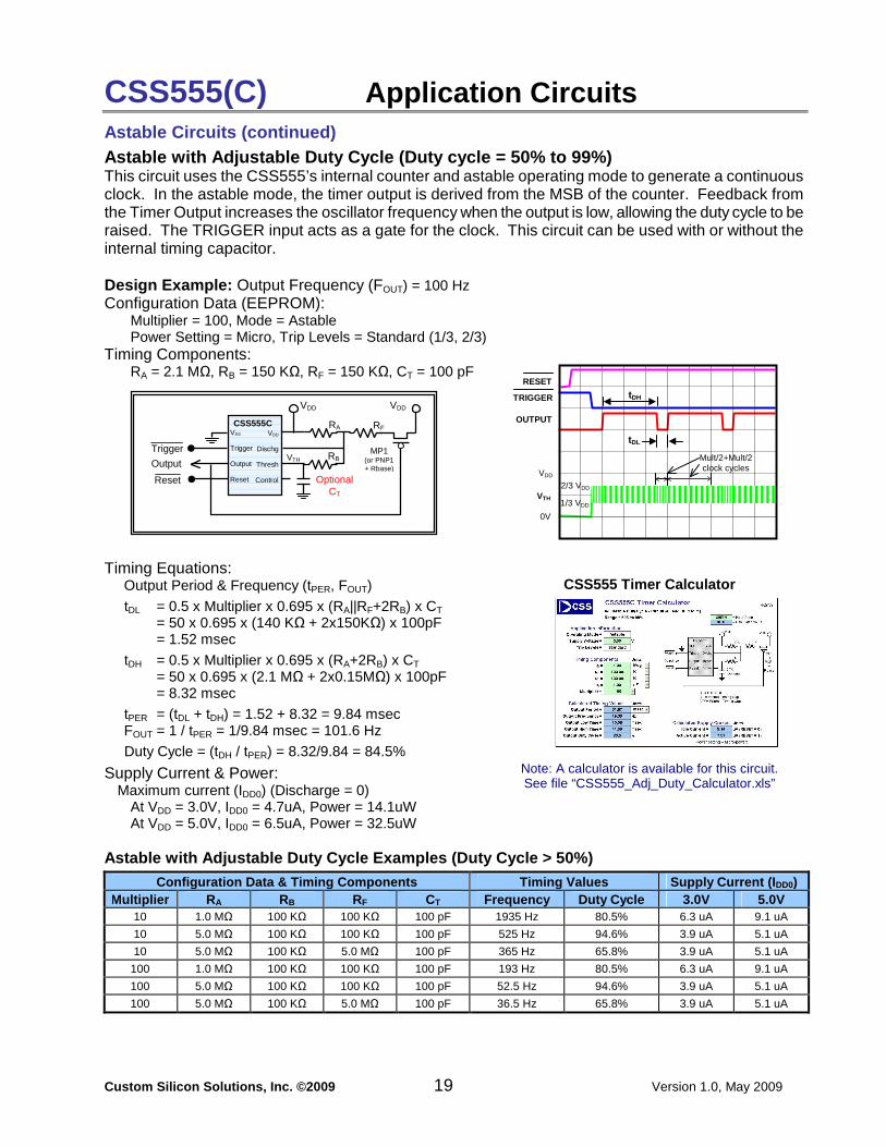
CSS555(C) Application Circuits Astable Circuits (continued) Astable with Adjustable Duty Cycle (Duty cycle = 50 % to 99%) This circuit uses the CSS555’s internal counter and astable operating mode to generate a continuous clock. In the astable mode, the timer output is derived from the MSB of the counter. Feedback from the Timer Output increases the oscillator frequency when the output is low, allowing the duty cycle to be raised. The TRIGGER input acts as a gate for the clock. This circuit can be used with or without the internal timing capacitor. Design Example: Output Frequency (FOUT) = 100 Hz Configuration Data (EEPROM):
Multiplier = 100, Mode = Astable Power Setting = Micro, Trip Levels = Standard (1/3, 2/3)
Timing Components: RA = 2.1 MΩ, RB = 150 KΩ, RF = 150 KΩ, CT = 100 pF
Timing Equations:
Output Period & Frequency (tPER, FOUT)
tDL = 0.5 x Multiplier x 0.695 x (RA||RF+2RB) x CT = 50 x 0.695 x (140 KΩ + 2x150KΩ) x 100pF = 1.52 msec
tDH = 0.5 x Multiplier x 0.695 x (RA+2RB) x CT = 50 x 0.695 x (2.1 MΩ + 2x0.15MΩ) x 100pF = 8.32 msec
tPER = (tDL + tDH) = 1.52 + 8.32 = 9.84 msec FOUT = 1 / tPER = 1/9.84 msec = 101.6 Hz
Duty Cycle = (tDH / tPER) = 8.32/9.84 = 84.5%
Supply Current & Power: Maximum current (IDD0) (Discharge = 0)
At VDD = 3.0V, IDD0 = 4.7uA, Power = 14.1uW At VDD = 5.0V, IDD0 = 6.5uA, Power = 32.5uW
CSS555 Timer Calculator
Note: A calculator is available for this circuit. See file “CSS555_Adj_Duty_Calculator.xls”
Astable with Adjustable Duty Cycle Examples (Duty C ycle > 50%)
Configuration Data & Timing Components Timing Values Supply Current (I DD0) Multiplier RA RB RF CT Frequency Duty Cycle 3.0V 5.0V
10 1.0 MΩ 100 KΩ 100 KΩ 100 pF 1935 Hz 80.5% 6.3 uA 9.1 uA
10 5.0 MΩ 100 KΩ 100 KΩ 100 pF 525 Hz 94.6% 3.9 uA 5.1 uA
10 5.0 MΩ 100 KΩ 5.0 MΩ 100 pF 365 Hz 65.8% 3.9 uA 5.1 uA
100 1.0 MΩ 100 KΩ 100 KΩ 100 pF 193 Hz 80.5% 6.3 uA 9.1 uA
100 5.0 MΩ 100 KΩ 100 KΩ 100 pF 52.5 Hz 94.6% 3.9 uA 5.1 uA
100 5.0 MΩ 100 KΩ 5.0 MΩ 100 pF 36.5 Hz 65.8% 3.9 uA 5.1 uA
VDD
RA
Trigger
Output
Reset
VDD
Dischg
Thresh
Control
CSS555C VSS
Trigger
Output
Reset
RB VTH
RF
MP1 (or PNP1 + Rbase)
VDD
Optional CT
TRIGGER
OUTPUT
VTH
0V
2/3 VDD
RESET
tDH
1/3 VDD
VDD
Mult/2+Mult/2 clock cycles
tDL
Custom Silicon Solutions, Inc. ©2009 20 Version 1.0, May 2009
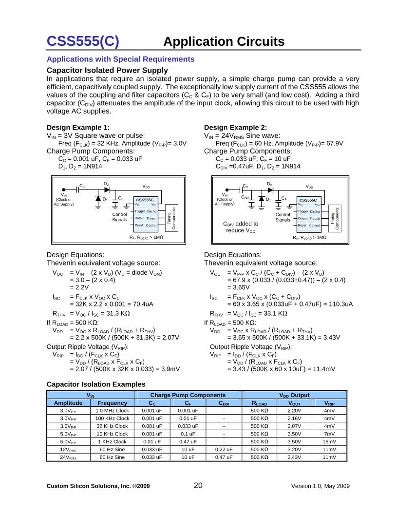
CSS555(C) Application Circuits Applications with Special Requirements Capacitor Isolated Power Supply In applications that require an isolated power supply, a simple charge pump can provide a very efficient, capacitively coupled supply. The exceptionally low supply current of the CSS555 allows the values of the coupling and filter capacitors (CC & CF) to be very small (and low cost). Adding a third capacitor (CDIV) attenuates the amplitude of the input clock, allowing this circuit to be used with high voltage AC supplies. Design Example 1: Design Example 2: VIN = 3V Square wave or pulse: VIN = 24VRMS Sine wave:
Freq (FCLK) = 32 KHz, Amplitude (VP-P)= 3.0V Freq (FCLK) = 60 Hz, Amplitude (VP-P)= 67.9V Charge Pump Components: Charge Pump Components:
CC = 0.001 uF, CF = 0.033 uF CC = 0.033 uF, CF = 10 uF D1, D2 = 1N914 CDIV =0.47uF, D1, D2 = 1N914
Design Equations: Design Equations: Thevenin equivalent voltage source: Thevenin equivalent voltage source:
VOC = VIN – (2 x VD) (VD = diode VON) VOC = VP-P x CC / (CC + CDIV) – (2 x VD) = 3.0 – (2 x 0.4) = 67.9 x (0.033 / (0.033+0.47)) – (2 x 0.4) = 2.2V = 3.65V
ISC = FCLK x VOC x CC ISC = FCLK x VOC x (CC + CDIV) = 32K x 2.2 x 0.001 = 70.4uA = 60 x 3.65 x (0.033uF + 0.47uF) = 110.3uA
RTHV = VOC / ISC = 31.3 KΩ RTHV = VOC / ISC = 33.1 KΩ
If RLOAD = 500 KΩ: If RLOAD = 500 KΩ: VDD = VOC x RLOAD / (RLOAD + RTHV) VDD = VOC x RLOAD / (RLOAD + RTHV) = 2.2 x 500K / (500K + 31.3K) = 2.07V = 3.65 x 500K / (500K + 33.1K) = 3.43V
Output Ripple Voltage (VRIP): Output Ripple Voltage (VRIP): VRIP = IDD / (FCLK x CF) VRIP = IDD / (FCLK x CF) = VDD / (RLOAD x FCLK x CF) = VDD / (RLOAD x FCLK x CF) = 2.07 / (500K x 32K x 0.033) = 3.9mV = 3.43 / (500K x 60 x 10uF) = 11.4mV
Capacitor Isolation Examples
VIN Charge Pump Components VDD Output Amplitude Frequency CC CF CDIV RLOAD VOUT VRIP
3.0VP-P 1.0 MHz Clock 0.001 uF 0.001 uF - 500 KΩ 2.20V 4mV
3.0VP-P 100 KHz Clock 0.001 uF 0.01 uF - 500 KΩ 2.16V 4mV
3.0VP-P 32 KHz Clock 0.001 uF 0.033 uF - 500 KΩ 2.07V 4mV
5.0VP-P 10 KHz Clock 0.001 uF 0.1 uF - 500 KΩ 3.50V 7mV
5.0VP-P 1 KHz Clock 0.01 uF 0.47 uF - 500 KΩ 3.50V 15mV
12VRMS 60 Hz Sine 0.033 uF 10 uF 0.22 uF 500 KΩ 3.20V 11mV
24VRMS 60 Hz Sine 0.033 uF 10 uF 0.47 uF 500 KΩ 3.43V 11mV
VDD
VIN (Clock or
AC Supply)
CF
VDD
Dischg
Thresh
Control
CSS555C VSS
Trigger
Output
Reset
D2
Tim
ing
Com
pone
nts
CC
D1
Control Signals
RA, RLOAD > 1MΩ
VDD
VIN (Clock or
AC Supply) CF
VDD
Dischg
Thresh
Control
CSS555C VSS
Trigger
Output
Reset
D2
Tim
ing
Com
pone
nts
CC
D1
Control Signals
RA, RLOAD > 1MΩ
CDIV
CDIV added to reduce VDD


