CS61C L18 Combinational Logic Blocks, Latches (1) Chae, Summer 2008 © UCB Albert Chae, Instructor...
38
CS61C L18 Combinational Logic Blocks, Latches (1) Chae, Summer 2008 © UCB Albert Chae, Instructor inst.eecs.berkeley.edu/~cs61c CS61C : Machine Structures Lecture #18 – Combinational Logic Blocks, Latches 2008-7-22
-
date post
21-Dec-2015 -
Category
Documents
-
view
222 -
download
3
Transcript of CS61C L18 Combinational Logic Blocks, Latches (1) Chae, Summer 2008 © UCB Albert Chae, Instructor...

CS61C L18 Combinational Logic Blocks, Latches (1) Chae, Summer 2008 © UCB
Albert Chae, Instructor
inst.eecs.berkeley.edu/~cs61c CS61C : Machine Structures
Lecture #18 – Combinational Logic Blocks, Latches
2008-7-22
CS61C L18 Combinational Logic Blocks, Latches (2) Chae, Summer 2008 © UCB
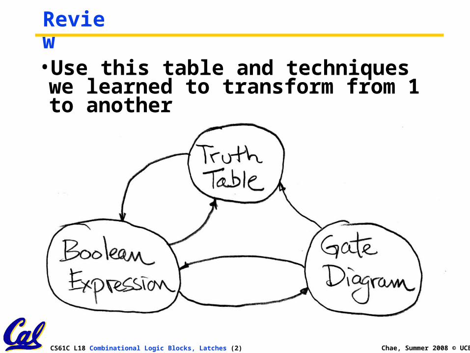
Review
•Use this table and techniques we learned to transform from 1 to another
CS61C L18 Combinational Logic Blocks, Latches (3) Chae, Summer 2008 © UCB
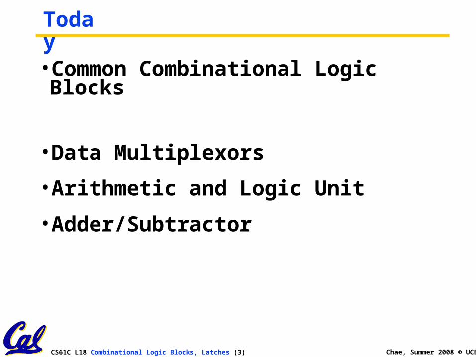
Today
•Common Combinational Logic Blocks
•Data Multiplexors
•Arithmetic and Logic Unit
•Adder/Subtractor
CS61C L18 Combinational Logic Blocks, Latches (4) Chae, Summer 2008 © UCB
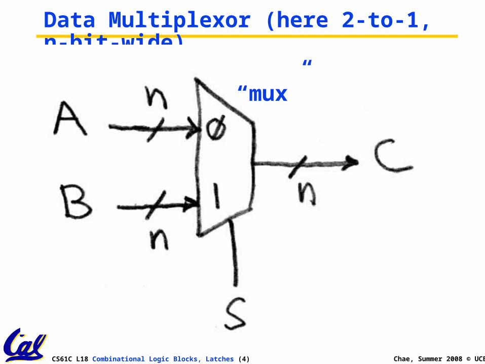
Data Multiplexor (here 2-to-1, n-bit-wide)
“mux”
CS61C L18 Combinational Logic Blocks, Latches (5) Chae, Summer 2008 © UCB
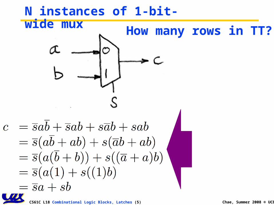
N instances of 1-bit-wide mux
How many rows in TT?

CS61C L18 Combinational Logic Blocks, Latches (6) Chae, Summer 2008 © UCB
How do we build a 1-bit-wide mux?
CS61C L18 Combinational Logic Blocks, Latches (7) Chae, Summer 2008 © UCB
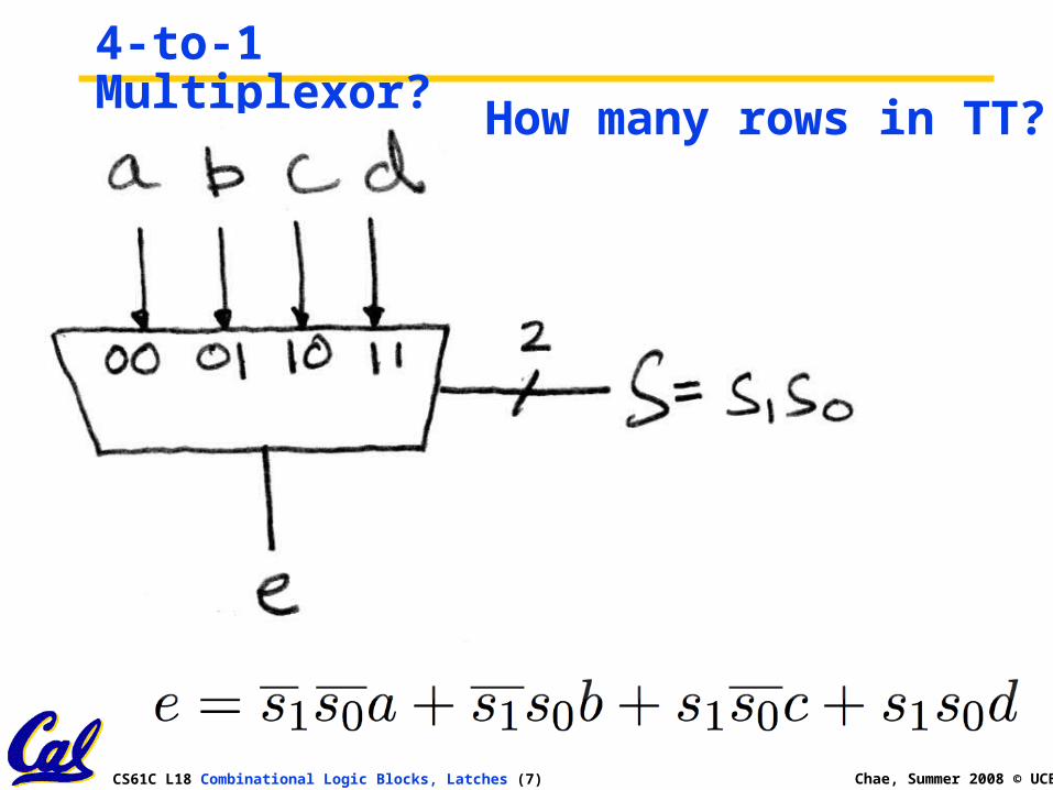
4-to-1 Multiplexor?
How many rows in TT?
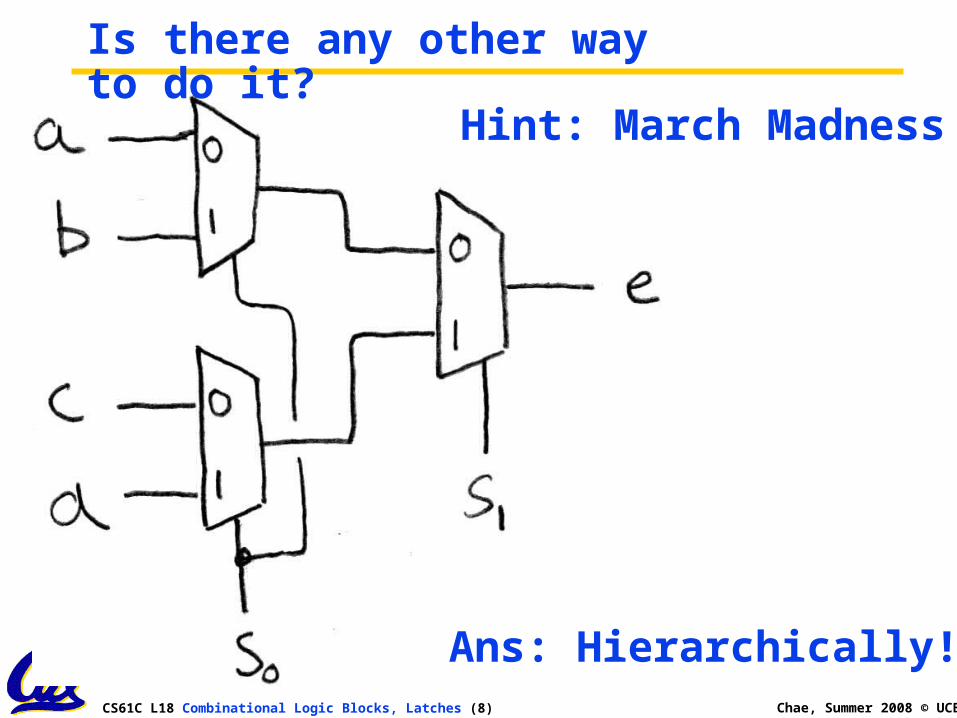
CS61C L18 Combinational Logic Blocks, Latches (8) Chae, Summer 2008 © UCB
Is there any other way to do it?
Hint: March Madness
Ans: Hierarchically!

CS61C L18 Combinational Logic Blocks, Latches (9) Chae, Summer 2008 © UCB
C
P
Q
0
1
D
D C0 P1 Q
Do you really understand NORs?• If one input is 1, what is a NOR?
• If one input is 0, what is a NOR?
A B NOR0 0 10 1 01 0 01 1 0
A
BNOR
A NOR
0 B’1 0A
_B
0NOR
CS61C L18 Combinational Logic Blocks, Latches (10) Chae, Summer 2008 © UCB
C
P
Q
0
1
D
D C0 P1 Q
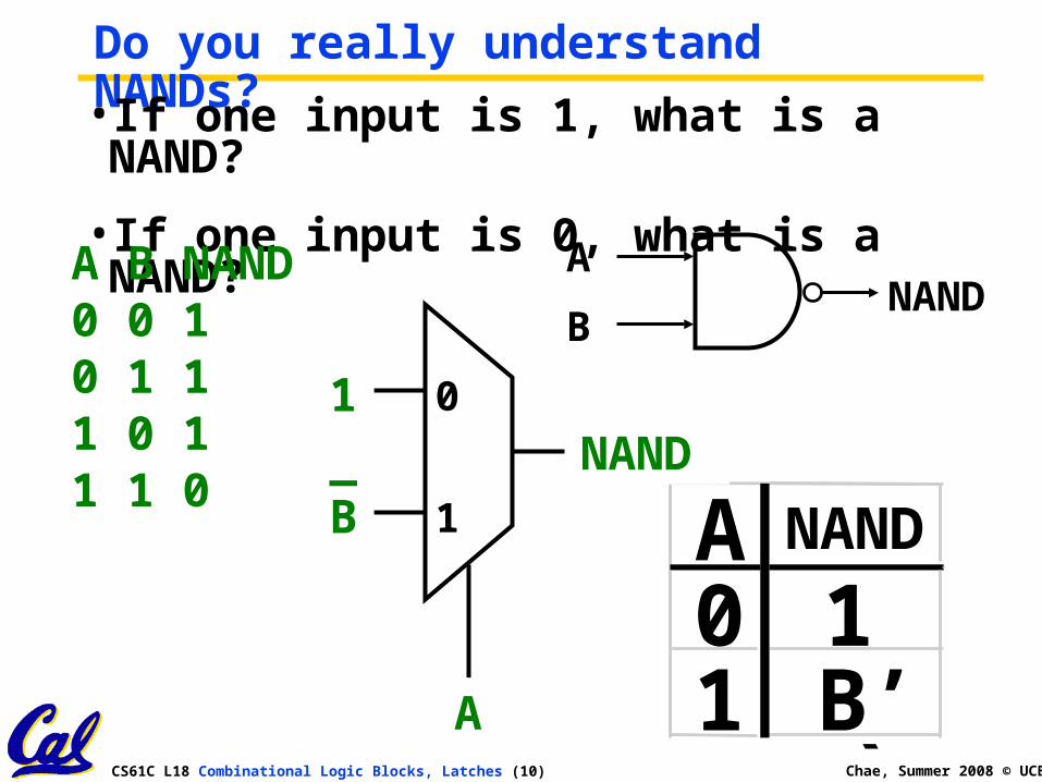
Do you really understand NANDs?• If one input is 1, what is a NAND?
• If one input is 0, what is a NAND?
A B NAND0 0 10 1 11 0 11 1 0
A NAND
0 11 B’A
1
_B
NAND
A
BNAND
CS61C L18 Combinational Logic Blocks, Latches (11) Chae, Summer 2008 © UCB
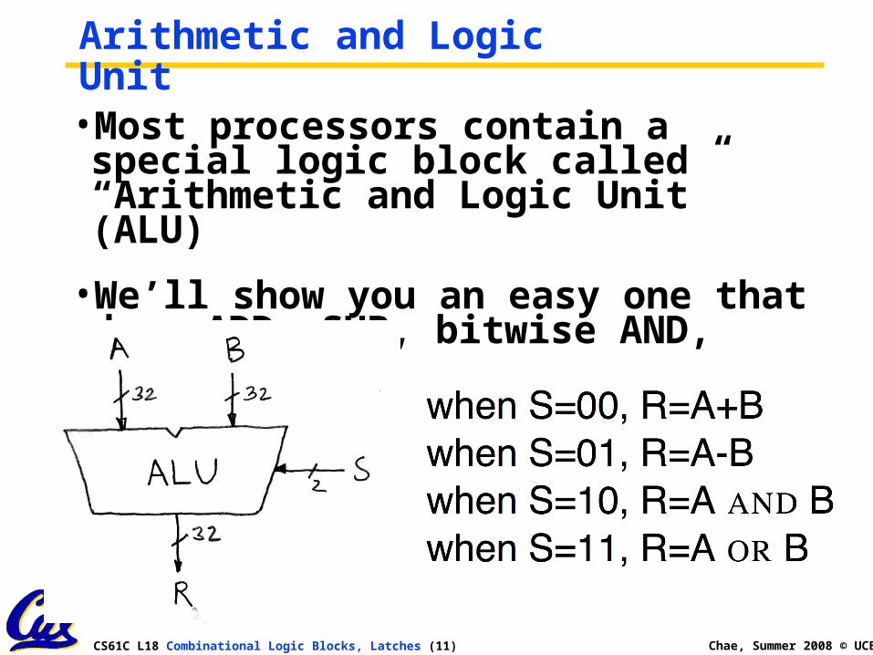
Arithmetic and Logic Unit
•Most processors contain a special logic block called “Arithmetic and Logic Unit” (ALU)
•We’ll show you an easy one that does ADD, SUB, bitwise AND, bitwise OR
CS61C L18 Combinational Logic Blocks, Latches (12) Chae, Summer 2008 © UCB
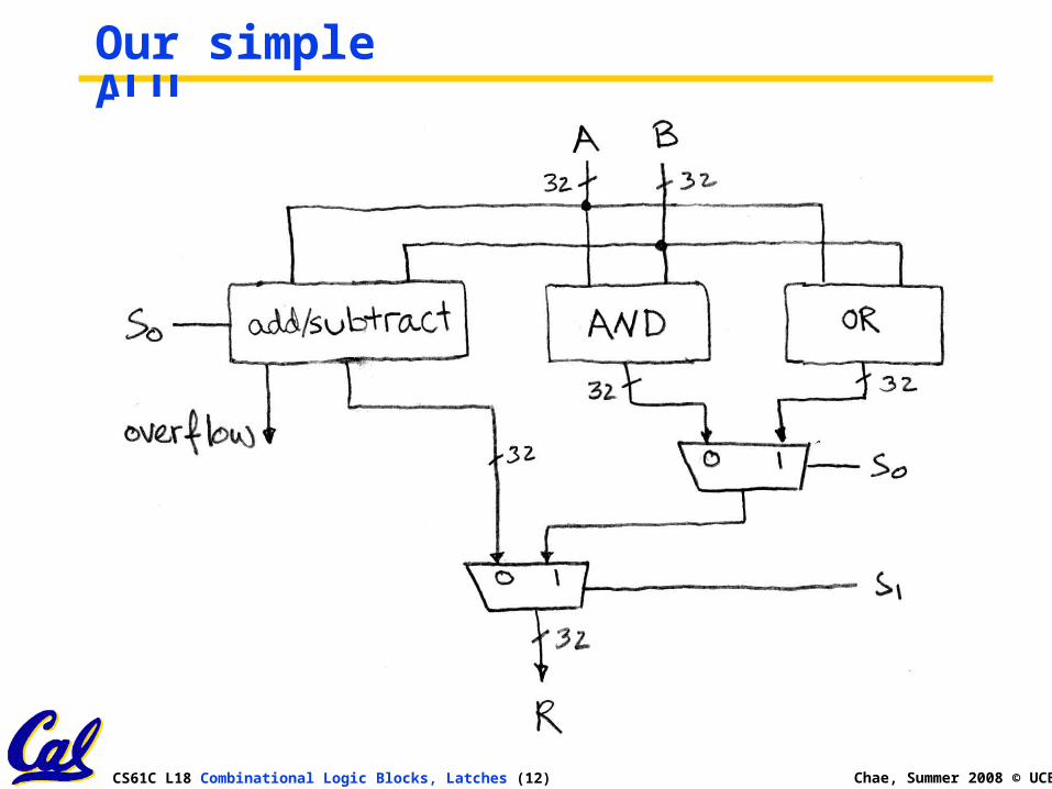
Our simple ALU
CS61C L18 Combinational Logic Blocks, Latches (13) Chae, Summer 2008 © UCB
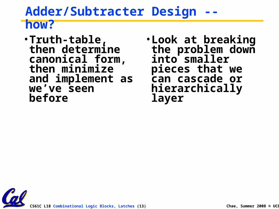
Adder/Subtracter Design -- how?• Truth-table, then
determine canonical form, then minimize and implement as we’ve seen before
• Look at breaking the problem down into smaller pieces that we can cascade or hierarchically layer
CS61C L18 Combinational Logic Blocks, Latches (14) Chae, Summer 2008 © UCB
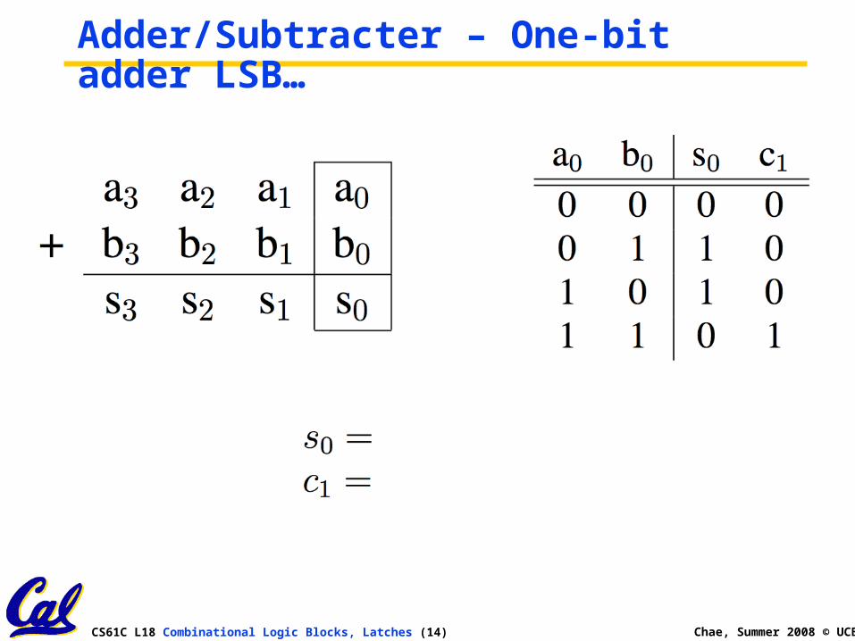
Adder/Subtracter – One-bit adder LSB…
CS61C L18 Combinational Logic Blocks, Latches (15) Chae, Summer 2008 © UCB
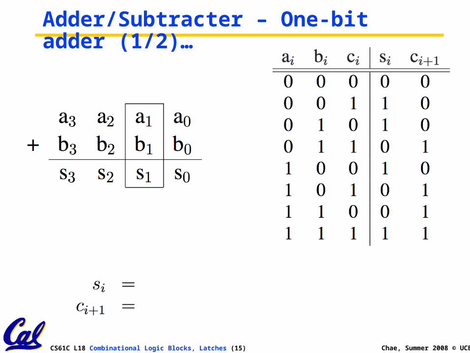
Adder/Subtracter – One-bit adder (1/2)…

CS61C L18 Combinational Logic Blocks, Latches (16) Chae, Summer 2008 © UCB
Adder/Subtracter – One-bit adder (2/2)…
CS61C L18 Combinational Logic Blocks, Latches (17) Chae, Summer 2008 © UCB
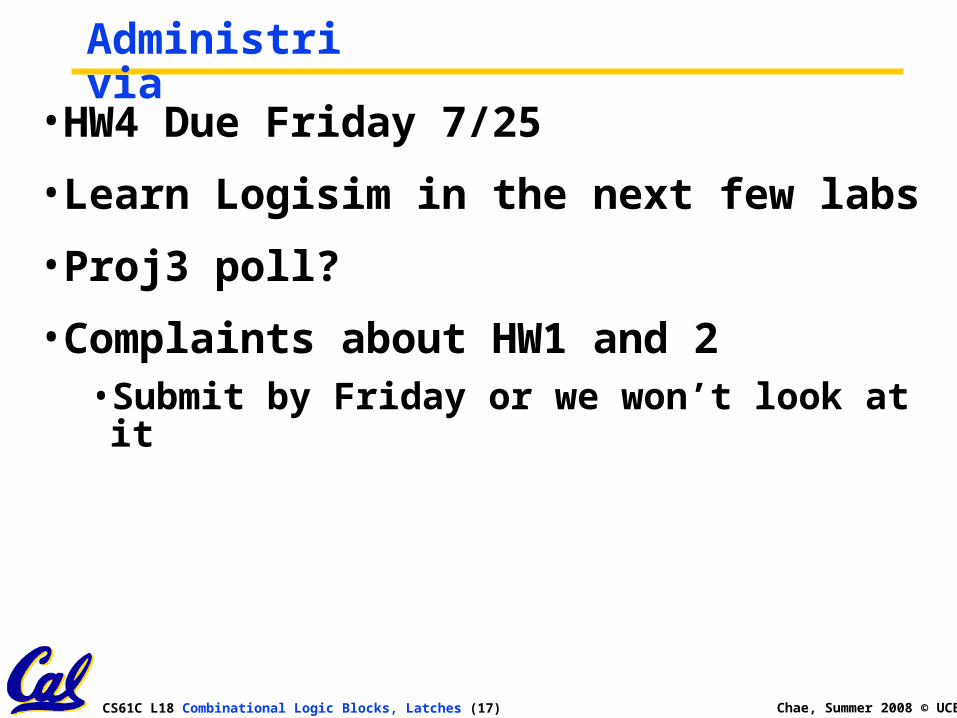
Administrivia
•HW4 Due Friday 7/25
•Learn Logisim in the next few labs
•Proj3 poll?
•Complaints about HW1 and 2• Submit by Friday or we won’t look at it
CS61C L18 Combinational Logic Blocks, Latches (18) Chae, Summer 2008 © UCB
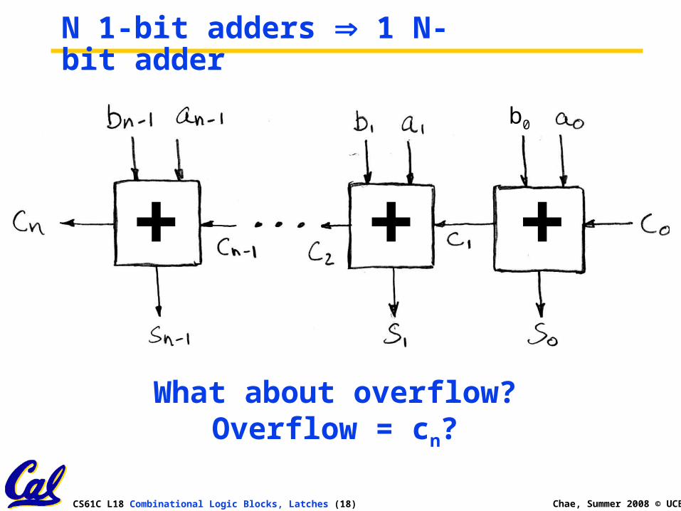
N 1-bit adders 1 N-bit adder
What about overflow?Overflow = cn?
+ + +
b0
CS61C L18 Combinational Logic Blocks, Latches (19) Chae, Summer 2008 © UCB
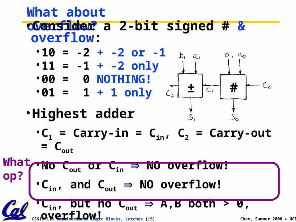
What about overflow?•Consider a 2-bit signed # & overflow:•10 = -2 + -2 or -1•11 = -1 + -2 only•00 = 0 NOTHING!•01 = 1 + 1 only
•Highest adder• C1 = Carry-in = Cin, C2 = Carry-out = Cout
• No Cout or Cin NO overflow!
• Cin, and Cout NO overflow!
• Cin, but no Cout A,B both > 0, overflow!
• Cout, but no Cin A,B both < 0, overflow!
± #
Whatop?
CS61C L18 Combinational Logic Blocks, Latches (20) Chae, Summer 2008 © UCB
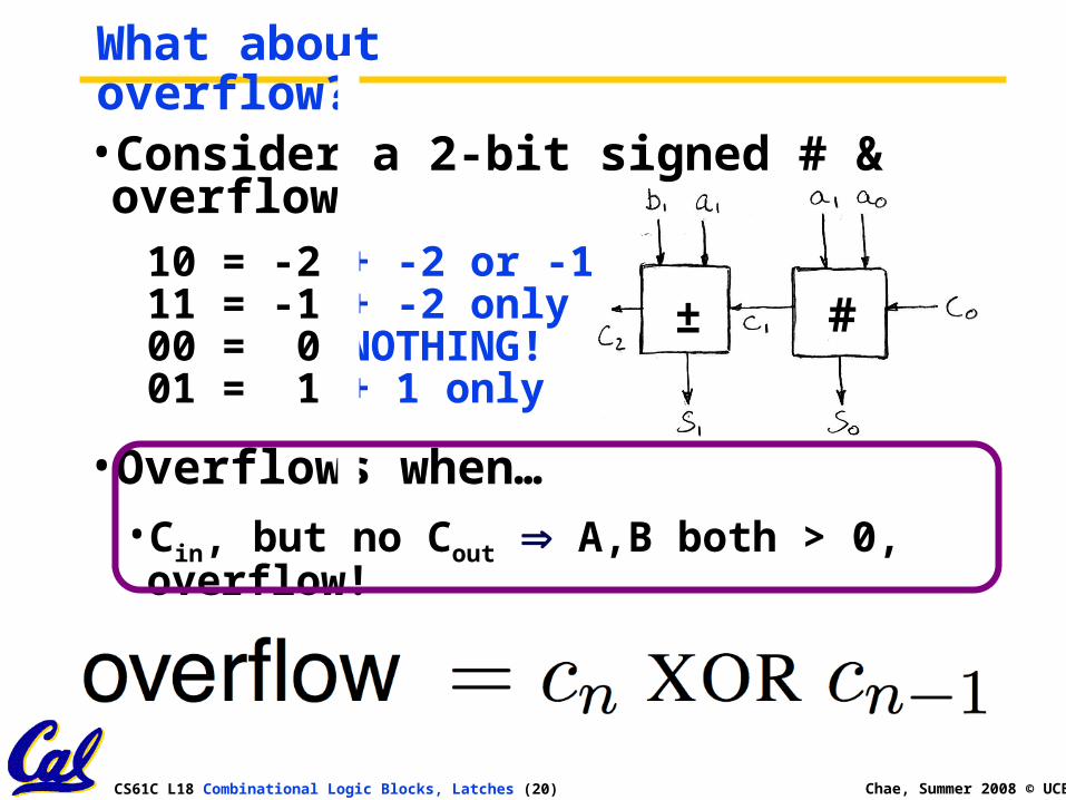
What about overflow?•Consider a 2-bit signed # & overflow:
10 = -2 + -2 or -111 = -1 + -2 only00 = 0 NOTHING!01 = 1 + 1 only
•Overflows when…• Cin, but no Cout A,B both > 0, overflow!
• Cout, but no Cin A,B both < 0, overflow!
± #
CS61C L18 Combinational Logic Blocks, Latches (21) Chae, Summer 2008 © UCB
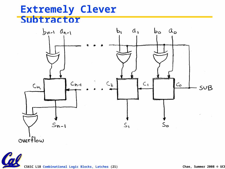
Extremely Clever Subtractor

CS61C L18 Combinational Logic Blocks, Latches (22) Chae, Summer 2008 © UCB
Taking advantage of sum-of-products
•Since sum-of-products is a convenient notation and way to think about design, offer hardware building blocks that match that notation
•One example isProgrammable Logic Arrays (PLAs)
•Designed so that can select (program) ands, ors, complements after you get the chip
• Late in design process, fix errors, figure out what to do later, …
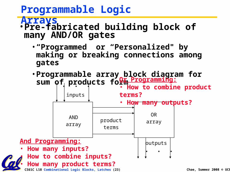
CS61C L18 Combinational Logic Blocks, Latches (23) Chae, Summer 2008 © UCB
• • •
inputs
ANDarray
• • •
outputs
ORarrayproduct
terms
Programmable Logic Arrays
• Pre-fabricated building block of many AND/OR gates
• “Programmed” or “Personalized" by making or breaking connections among gates
• Programmable array block diagram for sum of products form
And Programming:• How many inputs?• How to combine inputs?• How many product terms?
Or Programming:• How to combine product terms?• How many outputs?
CS61C L18 Combinational Logic Blocks, Latches (24) Chae, Summer 2008 © UCB
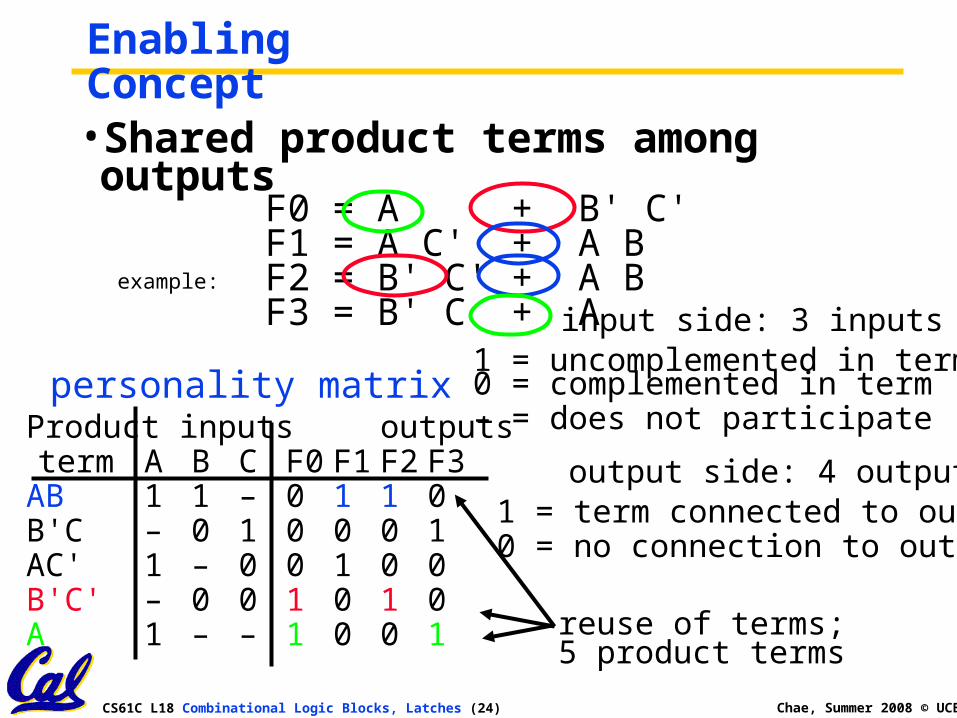
example:
F0 = A + B' C'F1 = A C' + A BF2 = B' C' + A BF3 = B' C + A
personality matrix1 = uncomplemented in term0 = complemented in term– = does not participate
1 = term connected to output0 = no connection to output
input side: 3 inputs
output side: 4 outputsProduct inputs outputsterm A B C F0 F1 F2 F3
AB 1 1 – 0 1 1 0B'C – 0 1 0 0 0 1AC' 1 – 0 0 1 0 0B'C' – 0 0 1 0 1 0A 1 – – 1 0 0 1 reuse of terms;
5 product terms
Enabling Concept•Shared product terms among outputs
CS61C L18 Combinational Logic Blocks, Latches (25) Chae, Summer 2008 © UCB
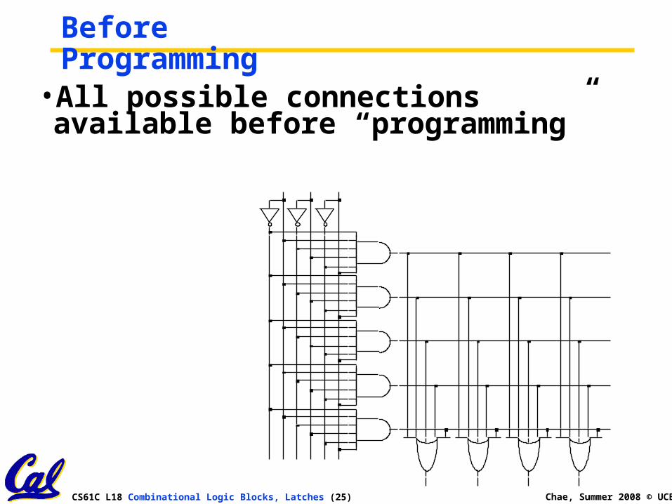
Before Programming•All possible connections available before “programming”
CS61C L18 Combinational Logic Blocks, Latches (26) Chae, Summer 2008 © UCB
A B C
F1 F2 F3F0
AB
B'C
AC'
B'C'
A
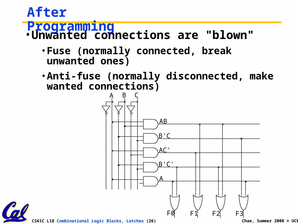
After Programming• Unwanted connections are "blown"
• Fuse (normally connected, break unwanted ones)
• Anti-fuse (normally disconnected, make wanted connections)
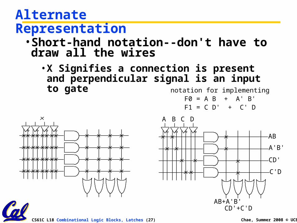
CS61C L18 Combinational Logic Blocks, Latches (27) Chae, Summer 2008 © UCB
notation for implementingF0 = A B + A' B'F1 = C D' + C' D
AB+A'B'CD'+C'D
AB
A'B'
CD'
C'D
A B C D
Alternate Representation• Short-hand notation--don't have to draw all
the wires• X Signifies a connection is present and
perpendicular signal is an input to gate
CS61C L18 Combinational Logic Blocks, Latches (28) Chae, Summer 2008 © UCB
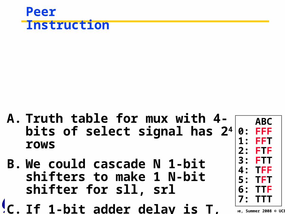
Peer Instruction
A. Truth table for mux with 4-bits of select signal has 24 rows
B. We could cascade N 1-bit shifters to make 1 N-bit shifter for sll, srl
C. If 1-bit adder delay is T, the N-bit adder delay would also be T
ABC0: FFF1: FFT 2: FTF3: FTT4: TFF5: TFT6: TTF7: TTT
CS61C L18 Combinational Logic Blocks, Latches (29) Chae, Summer 2008 © UCB
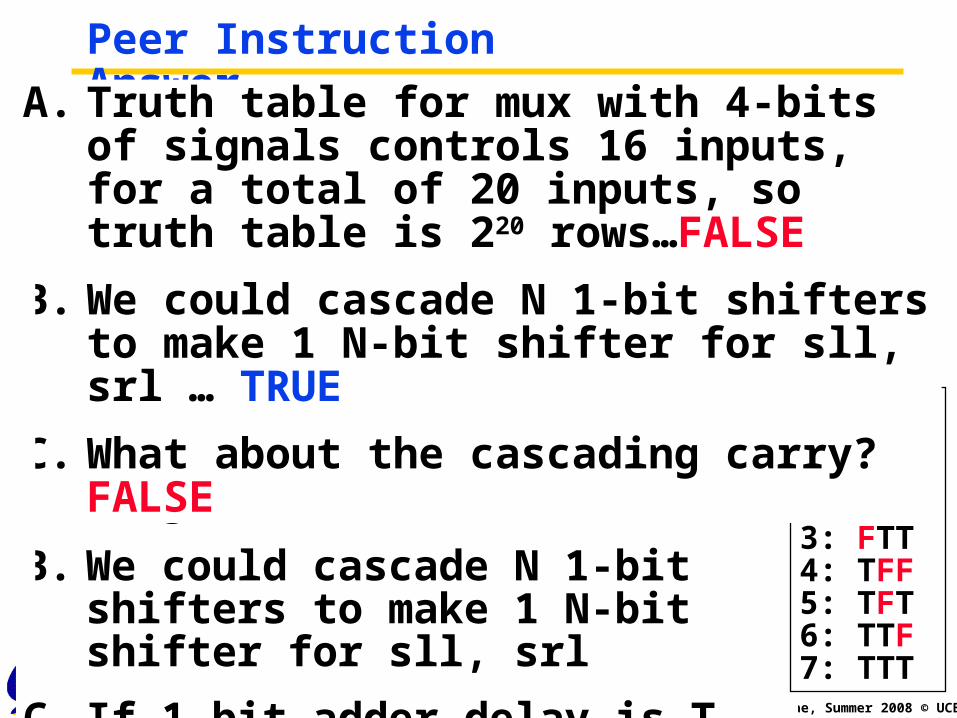
Peer Instruction Answer
A. Truth table for mux with 4-bits of signals is 24 rows long
B. We could cascade N 1-bit shifters to make 1 N-bit shifter for sll, srl
C. If 1-bit adder delay is T, the N-bit adder delay would also be T
ABC0: FFF1: FFT 2: FTF3: FTT4: TFF5: TFT6: TTF7: TTT
A. Truth table for mux with 4-bits of signals controls 16 inputs, for a total of 20 inputs, so truth table is 220 rows…FALSE
B. We could cascade N 1-bit shifters to make 1 N-bit shifter for sll, srl … TRUE
C. What about the cascading carry? FALSE
CS61C L18 Combinational Logic Blocks, Latches (30) Chae, Summer 2008 © UCB
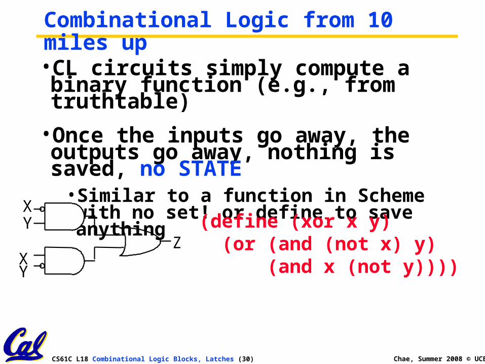
Combinational Logic from 10 miles up
•CL circuits simply compute a binary function (e.g., from truthtable)
•Once the inputs go away, the outputs go away, nothing is saved, no STATE
• Similar to a function in Scheme with no set! or define to save anything
•How does the computer remember data? [e.g., for registers]
XY
XY
Z(define (xor x y) (or (and (not x) y) (and x (not y))))
CS61C L18 Combinational Logic Blocks, Latches (31) Chae, Summer 2008 © UCB
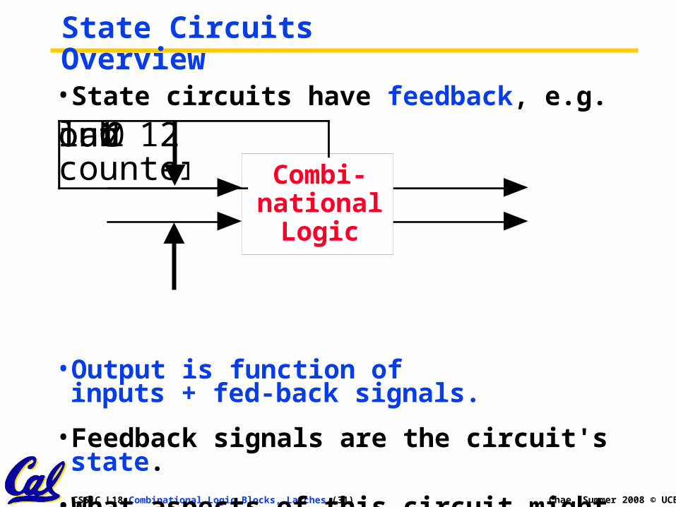
State Circuits Overview
• State circuits have feedback, e.g.
•Output is function ofinputs + fed-back signals.
• Feedback signals are the circuit's state.
•What aspects of this circuit might cause complications?
lab 12counterin0in1out0out1
Combi-national
Logic
CS61C L18 Combinational Logic Blocks, Latches (32) Chae, Summer 2008 © UCB
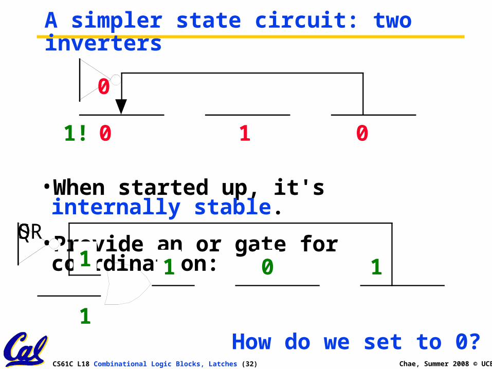
A simpler state circuit: two inverters
•When started up, it's internally stable.
•Provide an or gate for coordination:
•What's the result?
ORQS
0 1 0
0 1 0
0
0
0
1!
1
1 01 1
How do we set to 0?
CS61C L18 Combinational Logic Blocks, Latches (33) Chae, Summer 2008 © UCB
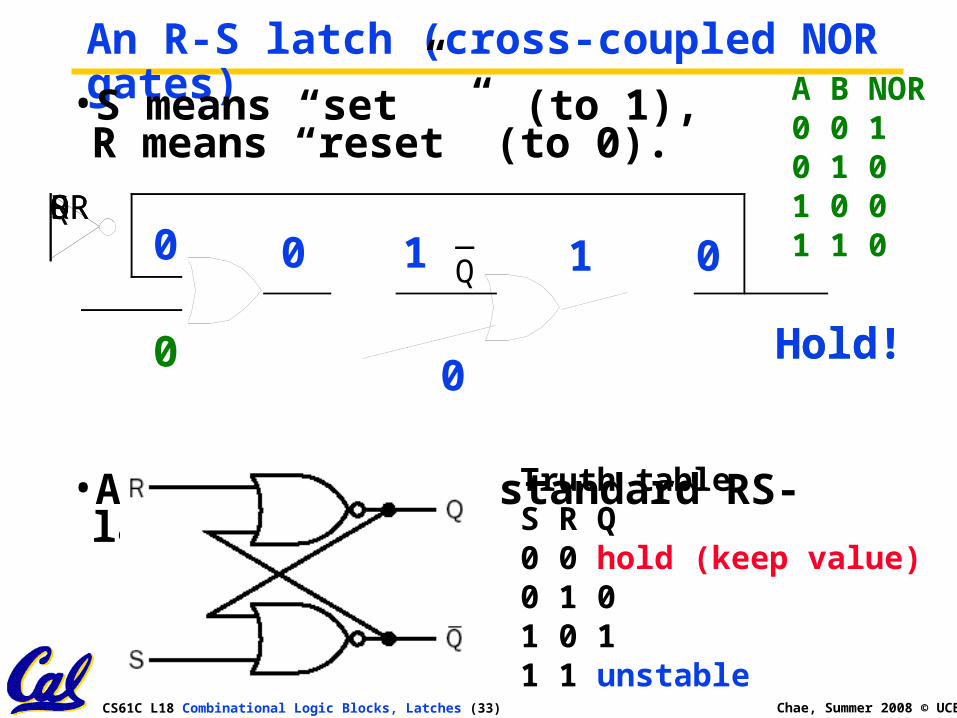
0
Hold!
An R-S latch (cross-coupled NOR gates)•S means “set” (to 1),R means “reset” (to 0).
•Adding Q’ gives standard RS-latch:
ORORSQR
Truth tableS R Q0 0 hold (keep value) 0 1 01 0 11 1 unstable
A B NOR0 0 10 1 01 0 01 1 0_
Q0 1 0
0
0
1
1 01 110
0
0 10 01
01
Hold!0
CS61C L18 Combinational Logic Blocks, Latches (34) Chae, Summer 2008 © UCB
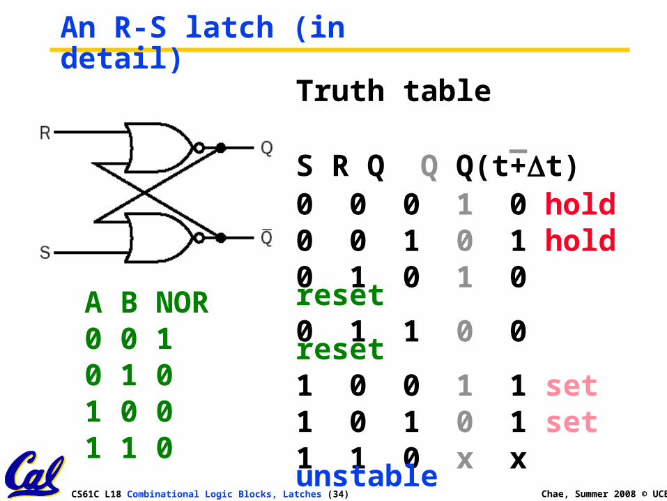
An R-S latch (in detail)
Truth table
_S R Q Q Q(t+t)0 0 0 1 0 hold0 0 1 0 1 hold0 1 0 1 0 reset0 1 1 0 0 reset1 0 0 1 1 set1 0 1 0 1 set1 1 0 x x unstable1 1 1 x x unstable
A B NOR0 0 10 1 01 0 01 1 0
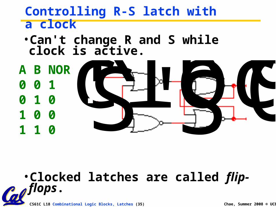
CS61C L18 Combinational Logic Blocks, Latches (35) Chae, Summer 2008 © UCB
Controlling R-S latch with a clock•Can't change R and S while clock is active.
•Clocked latches are called flip-flops.
clock'S' Q'QR'RS
A B NOR0 0 10 1 01 0 01 1 0
CS61C L18 Combinational Logic Blocks, Latches (36) Chae, Summer 2008 © UCB
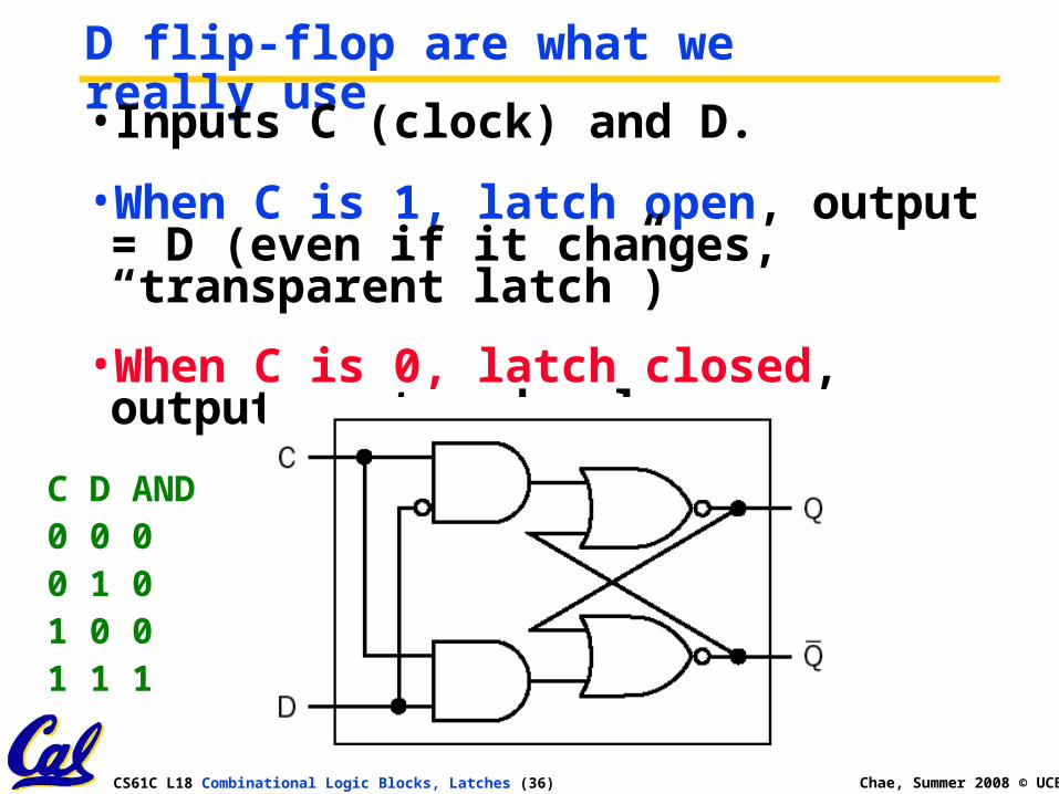
D flip-flop are what we really use• Inputs C (clock) and D.
•When C is 1, latch open, output = D (even if it changes, “transparent latch”)
•When C is 0, latch closed, output = stored value.
C D AND0 0 00 1 01 0 01 1 1
CS61C L18 Combinational Logic Blocks, Latches (37) Chae, Summer 2008 © UCB
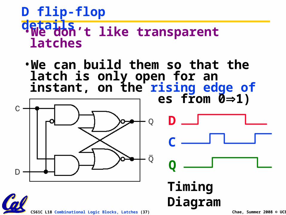
D flip-flop details•We don’t like transparent latches
•We can build them so that the latch is only open for an instant, on the rising edge of a clock (as it goes from 01)
D
C
Q
Timing Diagram
CS61C L18 Combinational Logic Blocks, Latches (38) Chae, Summer 2008 © UCB
“And In conclusion…”•Use muxes to select among input
• S input bits selects 2S inputs• Each input can be n-bits wide, indep of S
•Can implement muxes hierarchically
•ALU can be implemented using a mux• Coupled with basic block elements
•N-bit adder-subtractor done using N 1-bit adders with XOR gates on input
• XOR serves as conditional inverter
•Latches are used to implement flip-flops