CS 250 VLSI System Design Lecture 13 High-Speed I/Ocs250/fa09/lectures/lec13.pdf · CS 250 VLSI...
30
UC Regents Fall 2009 © UCB CS 250 L13: High-Speed I/O 2009-10-8 John Wawrzynek and Krste Asanovic with John Lazzaro CS 250 VLSI System Design Lecture 13 – High-Speed I/O www-inst.eecs.berkeley.edu/~cs250/ TA: Yunsup Lee 1
Transcript of CS 250 VLSI System Design Lecture 13 High-Speed I/Ocs250/fa09/lectures/lec13.pdf · CS 250 VLSI...

UC Regents Fall 2009 © UCBCS 250 L13: High-Speed I/O
2009-10-8John Wawrzynek and Krste Asanovic
with John Lazzaro
CS 250 VLSI System Design
Lecture 13 – High-Speed I/O
www-inst.eecs.berkeley.edu/~cs250/
TA: Yunsup Lee
1

UC Regents Fall 2009 © UCBCS 250 L13: High-Speed I/O
Abstract
This paper reviews the technology of high-performance
electrical signaling, presents the current state of the art, and
projects future directions. We have demonstrated equal-
ized electrical signaling between CMOS integrated circuits
at data rates of 4Gb/s. As the factors that determine this
signaling rate all scale with improving technology, we
expect the data rates of high-performance electrical signal-
ing systems to improve on a Moore’s Law curve. The fre-
quency-dependent attenuation of copper wires sets a
bandwidth-distance squared (Bd2) limit on the distance one
can signal at a given data rate. Equalizing the channel can-
cels inter-symbol interference caused by this attenuation
and greatly increases signaling distance. In the limit of
perfect equalization, distance is ultimately limited by ther-
mal noise in the receiver. At this limit, we calculate that a
4Gb/s system will be capable of operating over 100m of
24-gauge cable without repeaters.
1. Introduction
Data communication or signaling is a dominant power,
performance, and cost factor in many digital systems. The
connection between processors, caches, and main memory
in computer systems; multiprocessor and multicomputer
interconnection networks; and high-speed network
switches are all critically dependent on signaling technol-
ogy.
Conventional CMOS signaling has been limited to data
rates of 100MHz or less and these data rates have not
scaled with improving technology. Costly wide buses and
high pin-count chips and modules have resulted from try-
ing to meet the bandwidth demands of modern systems
using this slow signaling technology.
We have recently demonstrated equalized CMOS I/O
drivers that operate at 4Gb/s over moderate length copper
interconnect [DP96, DP97, PDT98]. These designs oper-
ate at data rates that are limited by timing jitter, signal rise-
time, and receiver aperture time all of which improve as
technology scales [DP98b, HYS]. Thus, we expect the
data rates of high-performance electrical signaling systems
to improve on a Moore’s Law curve.
At a given signaling rate, the distance over which one
can reliably transmit a signal is limited by the frequency-
dependent attenuation of the transmission medium. This
limitation can be expressed as a bandwidth-distance
squared, Bd2, product. This Bd2 product is proportional to
the square of the attenuation that can be tolerated by the
system.
Only a few dB of frequency-dependent attenuation can
be tolerated by an unequalized signaling system before
inter-symbol interference overwhelms the signal. Equaliz-
ing the channel cancels this inter-symbol interference
increasing the tolerable attenuation and quadratically
increasing the Bd2 product. To date we have demonstrated
a signaling system that is capable of equalizing up to 10dB
of frequency-dependent attenuation. We expect to be able
to equalize greater levels of attenuation as this technology
evolves.
With perfect equalization, a signaling system is ulti-
mately limited by thermal (Johnson) noise in the receiver.
Using conservative assumptions about system perfor-
mance, we calculate that a Johnson-noise limited system
will be capable of communicating over 100m of 24-gauge
cable at 4Gb/s without repeaters.
The remainder of this paper discusses the technology of
high-performance electrical signaling in more detail. We
begin in Section 2 by examining the limitations of conven-
tional CMOS signaling and show how they are overcome
by low-swing, incident-wave signaling. In Section 3 we
explore the limitations on signaling rate due to electronics
and wire. We see that the electronic factors that limit sig-
naling rate all improve as semiconductor technology
scales. We also see that wire characteristics place a limit
on the Bd2 product of a signaling technology and that the
magnitude of this product is heavily dependent on equal-
ization. We review our experience building an equalized
CMOS signaling system in Section 4 and discuss plans for
reducing the size and power required by this system.
2. High-Performance Signaling Basics
2.1 Traditional CMOS Signaling
Traditional CMOS signaling systems are limited to data
rates of 100Mb/s per wire or less and dissipate large
amounts of energy per bit transmitted. More importantly,
traditional CMOS signaling rates do not scale with improv-
ing semiconductor technology. Because of this, many
High-Performance Electrical Signaling
William J. Dally1, Ming-Ju Edward Lee1, Fu-Tai An1, John Poulton2, and Steve Tell2
1Computer Systems Laboratory
Stanford University
2Department of Computer Science
University of North Carolina - Chapel Hill
CMOS High-Speed I/Os — Present and Future
M.-J. Edward Lee1, William J. Dally1,2, Ramin Farjad-Rad1, Hiok-Tiaq Ng1,Ramesh Senthinathan1, John Edmondson1, and John Poulton1
1Velio Communications, Inc. 2Stanford UniversityMilpitas, CA Stanford, CA
Abstract
High-speed I/O circuits, once used only for PHYs, arenow widely used for intra-system signaling as well becauseof their bandwidth, power, area, and cost advantages. Thistechnology enables chips with over 1 Tb/s of I/O bandwidthtoday and over 10 Tb/s of bandwidth by 2010 as both sig-naling rates and number of high-speed I/Os increase withprocess scaling. Key technologies that enable this growth inI/O performance include low-jitter clock circuits and equal-ized signaling. An analysis of clock jitter and channel inter-ference suggests that signaling rates should track transistorperformance to rates of at least 40 Gb/s over boards, back-planes, and short-distance cables.
1. Introduction
High-speed input/output circuits are becoming increas-ingly critical as technology scales to increase system band-width and decrease power dissipation, die area and systemcost. Once used primarily for serial PHYs, high-speed I/Ocircuits are rapidly becoming the technology of choice forall intra-system connections as well. High-speed I/Os inte-grated in large numbers enable chips with over 1 Tb/s ofI/O bandwidth today. Furthermore, the per-pin bandwidthscales with device speed, at !20% per year. As this trendcontinues, chips with many hundreds of 20 Gb/s I/Os willbe feasible by 2010.
High-speed I/Os use incident-wave signaling in which asignal is detected on its first traversal of the signal line (theincident wave) and absorbed by a receive termination. Thisenables the data bandwidth to scale with transistor perfor-mance, independent of the length of the line. At high datarates, several bits may be in transit at once — pipelinedalong the length of the line. In contrast, traditional I/O de-signs, e.g., LVCMOS, have a bandwidth that is limited bythe length of the signal line rather than transistor perfor-mance. Without matched terminations, these I/O systemshave to ring-up the signal wire over several round-trip de-lays to reliably send one bit. Their data bandwidth is tiedto the length of the line, independent of transistor perfor-
mance, resulting in a bottleneck as bandwidth demands in-crease.
More than half of the power dissipation of many sys-tems today is I/O power, and the fraction of power due toI/O is increasing. The dynamic power of a logic functionscales as α3 (where gate length scales as α) while a portionof I/O power scales only with α, because a certain amountof current must be delivered to a load that is matched tothe line impedance to reliably detect the signal. The mini-mum current required per I/O is nearly constant, indepen-dent of bit rate; thus high-speed I/Os give more bandwidthfor this fixed power. Furthermore, the additional power re-quired to build a sophisticated high-speed I/O often scaleswith α3, like the core logic. Thus, a better process technol-ogy not only enables a higher bandwidth per channel butalso reduces the energy consumed per bit.
There are two fundamental challenges to continued scal-ing of high-speed I/Os: band-limited channels and timinguncertainty. As data rates increase, channel bandwidth be-comes limited by the frequency-dependent loss (FDL) ofthe channel. The distance that a signal can be reliably prop-agated decreases with the square-root of signal bandwidthfor cables (where skin-effect dominates) and linearly withsignal bandwidth for circuit boards (where dielectric ab-sorption dominates). Equalization can cancel the frequency-dependent part of the attenuation. However, the magnitudeof the attenuation is ultimately a limiting factor. Also, as at-tenuation levels increase, care must be taken to avoid near-end cross-talk, which is becoming a significant problem inlegacy systems.
As signal rates scale, the timing jitter of a high-speedI/O must decrease to remain a constant fraction of a bit timeor unit interval (UI). Power supply noise, substrate noiseand thermal noise are the most important contributors toclock jitter. Fortunately, our analyses show that by increas-ing reference clock frequencies and devoting a larger frac-tion of I/O area to clock circuits, timing jitter can be madeto scale with bit time. Overall, it appears that there are nomajor obstacles to achieving 40 Gb/s signaling rates overboards, backplanes, and short-distance cables (tens of me-ters). Hence signaling rates should continue to scale withtransistor performance to at least this speed.
The remainder of this paper describes high-speed I/O cir-
!"#$%%&'()*+#,+-.%+/0*-+1(-%"(2-'#(23+4#(,%"%($%+#(+4#567-%"+8%*')(+91448:;<=+0;><?>@;@A;<+B+0CD;;+E+/;;<+1FFF+
Figures of Merit to Characterize the Importanceof On-Chip Inductance
Yehea I. Ismail, Eby G. Friedman, and Jose L. Neves1
Department of Electrical EngineeringUniversity of Rochester
Rochester, New York 14627
1IBM Microelectronics
1580 Route 52 East Fishkill, New York 12533
Abstract - A closed form solution for the output signal of a CMOS
inverter driving an RLC transmission line is presented. This solution is
based on the alpha power law for deep submicrometer technologies. Two
figures of merit are presented that are useful for determining if a section
of interconnect should be modeled as either an RLC or an RC impedance.
The damping factor of a lumped RLC circuit is shown to be a useful figure
of merit. The second useful figure of merit considered in this paper is the
ratio of the rise time of the input signal at the driver of an interconnect
line to the time of flight of the signals across the line. AS/X circuit
simulations of an RLC transmission line and a five section RC ! circuit
based on a 0.25 µm IBM CMOS technology are used to quantify and
determine the relative accuracy of an RC model. One primary result of
this study is evidence demonstrating that a range for the length of the
interconnect exists for which inductance effects are prominent.
Furthermore, it is shown that under certain conditions, inductance
effects are negligible despite the length of the section of interconnect.
I. IntroductionIt has become well accepted that interconnect delay dominates
gate delay in current deep submicrometer VLSI circuits [1]-[4].
With the continuous scaling of technology and increased die area,
this situation is expected to become worse. In order to properly
design complex circuits, more accurate interconnect models and
signal propagation characterization are required. Historically,
interconnect has been modeled as a single lumped capacitance in
the analysis of the performance of on-chip interconnects. With the
scaling of technology and increased chip sizes, the cross-sectional
area of wires has been scaled down while interconnect length has
increased. The resistance of the interconnect has therefore become
significant, requiring the use of more accurate RC delay models. At
first interconnect was modeled as a lumped RC circuit. To further
improve accuracy, the interconnect has been modeled as a
distributed RC circuit (multiple T or ! sections) for those nets
requiring more accurate delay models. A well known method used to
determine which nets require more accurate delay models is to
This research was supported in part by the National Science Foundation
under Grant No. MIP-9423886 and Grant No. MIP-9610108, the ArmyResearch Office under Grant No. DAAH04-93-G-0323, a grant from theNew York State Science and Technology Foundation to the Center forAdvanced Technology - Electronic Imaging Systems, and by grants from theXerox Corporation, IBM Corporation, and Intel Corporation.
compare the driver resistance Rtr and the load capacitance C
L to the
total resistance and capacitance of the interconnect line, Rt and C
t
[5], [6]. Typically, those nets that require more accurate RC models
are longer, more highly resistive nets.
Currently, inductance is becoming more important with faster
on-chip rise times and longer wire lengths. Wide wires are
frequently encountered in clock distribution networks and in upper
metal layers. These wires are low resistive lines that can exhibit
significant inductive effects. Furthermore, performance
requirements are pushing the introduction of new materials for low
resistance interconnect [7]. In the limiting case, high temperature
superconductors may become commercially available [8]. With
these trends it is becoming crucial to be able to determine which
nets within a high speed VLSI circuit exhibit prominent inductive
effects.
The focus of this paper is the introduction of simple figures of
merit that can be used as criteria to determine which nets require
more accurate transmission line models. The equations describing
the signal behavior of an RLC transmission line are provided in
section II, along with a closed form solution for the output signal
of a CMOS inverter driving an RLC transmission line based on the
alpha power law [9] for deep submicrometer (DSM) technologies.
The damping factor of a lumped RLC circuit and the rise time of the
input signal at the driver of the interconnect are used to derive two
figures of merit that describe the relative significance of
inductance of a local interconnect line. These figures of merit are
presented in section II. In section III, the two figures of merit
described in section II are combined to define a range of the length
of interconnect at which inductance become important. AS/X
circuit simulations [10] are also compared in this section to the
analytical results presented in the previous section. Finally, some
conclusions are offered in section IV.
II. Theoretical Analysis of Inductance Effects in RLCInterconnect
The behavior of waves traveling across an RLC transmission
line is explained in this section. The attenuation that a wave
exhibits as it travels along a line is compared to the damping
factor of a lumped RLC circuit representation of the same line. It i s
shown in subsection A that the damping factor of a lumped RLC
circuit representation of a line can be a useful figure of merit to
determine the relative importance of inductance. A closed form
solution for the output voltage of a CMOS gate driving an RLC
transmission line is presented in subsection B. A closed form
solution for a CMOS gate driving a single RC T section
representation of the line is also presented. Both solutions are
compared for different values of attenuation to further investigate
the damping factor as a useful figure of merit. The two solutions are
also compared with different input transition times which leads to
the second figure of merit in this paper. It is shown that the ratio
Permission to make digital/hard copy of all or part of this work for personal orclassroom use is granted without fee provided that copies are not made or distributedfor profit or commercial advantage, the copyright notice, the title of publication andits date appear, and notice is given that copying is by permission of ACM, Inc. Tocopy otherwise, to republish, to post on servers or to redistribute to lists, requiresprior specific permission and/or fee.
DAC 98, San Francisco, California© 1998 ACM 1-58113-049-x/98/06 $3.50
834 IEEE JOURNAL OF SOLID-STATE CIRCUITS, VOL. 38, NO. 5, MAY 2003
Near Speed-of-Light Signaling Over On-Chip Electrical Interconnects
Richard T. Chang, Student Member, IEEE, Niranjan Talwalkar, Student Member, IEEE, C. Patrick Yue, Member, IEEE,and S. Simon Wong, Fellow, IEEE
Abstract—The propagation limits of electrical signals forsystems built with conventional silicon processing are explored.A design which takes advantage of the inductance-dominatedhigh-frequency regime of on-chip interconnect is shown capableof transmitting data at velocities near the speed of light. In a0.18- m six-level aluminum CMOS technology, an overall delayof 283 ps for a 20-mm-long line, corresponding to a propagationvelocity of one half the speed of light in silicon dioxide, has beendemonstrated. This approach offers a five times improvement indelay over a conventional repeater-insertion strategy.
Index Terms—Integrated circuit interconnections, microstrip,monolithic integrated circuits, on-chip interconnect, phase modu-lation, transmission lines.
I. INTRODUCTION
INTERCONNECT has long been perceived to be a bot-
tleneck in present and future high-performance digital
integrated circuits because of its inability to keep pace with
advances in transistor speeds [1]. Consequently, alternative
solutions such as on-chip optical interconnects have been
proposed in order to avoid the problems associated with global
on-chip wires altogether [2]. However, due to technology in-
compatibility, cost considerations, and nonnegligible delays in
converting the signals between optical and electrical domains,
this has not yet been shown to be practical. In this brief, we
explore the velocity limitations for systems built with conven-
tional silicon processing and show that data transmission at
near the speed of light is possible in an all-electrical system.
II. LIMITATIONS OF CONVENTIONAL REPEATER-INSERTION
APPROACH
The most common means of global communication is
through the use of wires with appropriately spaced repeaters
[3]. Based on a 0.18- m 1.8-V CMOS six-level aluminum in-
terconnect technology, simulations were carried out in HSPICE
for minimum-width (0.44- m), minimum-spacing (0.46- m)
lines with varying number of repeaters for a fixed overall
distance (Fig. 1) [4]. The optimized minimum delay, including
both wire and buffer delays, is about 1.35 ns for propagation
over a length of 20 mm, translating into an effective velocity of
about one tenth of the speed of light in silicon dioxide . This
optimized delay configuration yields a power dissipation of
30 mW, assuming 1-GHz switching, with an average transition
time of 200 ps.
Manuscript received July 27, 2002; revised December 23, 2002. This workwas supported by theMARCO Interconnect Focus Center and the Taiwan Semi-conductor Manufacturing Corporation (TSMC).The authors are with the Center for Integrated Systems, Stanford University,
Stanford, CA 94305-4070 USA (e-mail: [email protected]).Digital Object Identifier 10.1109/JSSC.2003.810060
Fig. 1. Simulated performance of minimum-sized interconnect (0.44- mwide, 0.46- m spacing for aluminum/silicon dioxide interconnects) withrepeaters.
Fig. 2. Frequency characteristics of 500-ps-wide digital pulse and typicalminimum-sized global wires. is the speed of light in silicon dioxide.
While the buffer delays can be improved by using more ad-
vanced technology and/or expending more power, the intrinsic
wire delay is fundamentally limited. To understand the reasons
for this, the power spectral density of a 500-ps digital pulse is
compared with the frequency-dependent characteristics of the
aforementioned minimum-sized wire without repeaters (Fig. 2).
The digital signal is broadband in nature, while the phase ve-
locity for signals propagating along the wire changes dramati-
cally over this frequency range. For transmission line systems,
the phase velocity, rather than the group velocity, is meaningful
to consider [5]. The telegrapher’s equation describes the signal
propagation as a function of time:
(1)
where is the distance along the wire, is time, is voltage,
and , , and are the resistance, inductance, and capacitance
0018-9200/03$17.00 © 2003 IEEE
1
Abstract - Clock recovery using phase-locked loops (PLL)with binary (bang-bang) or ternary-quantized phase detectorshas become increasingly common starting with the advent offully monolithic clock and data recovery (CDR) Circuits in thelate 1980’s. Bang-bang CDR circuits have the unique advan-tages of inherent sampling phase alignment, adaptability tomulti-phase sampling structures, and operation at the highestspeed at which a process can make a working flip-flop. Thispaper gives insight into the behavior of the nonlinear bang-bang PLL loop dynamics, giving approximate equations forloop jitter, recovered clock spectrum, and jitter tracking per-formance as a function of various design parameters. A novelanalysis shows that the bang-bang loop output jitter grows asthe square-root of the input jitter as contrasted with the lineardependence of the linear PLL.
I. INTRODUCTION
Prior to the advent of fully monolithic designs, clock recoverywas traditionally performed with some variant of the circuit in Fig.1. The clock frequency component was typically extracted from
the data stream using some combination of differentiation, rectifi-cation and filtering. The bandpass frequency filtering was pro-vided by LC tank, surface acoustic wave (SAW) filter, dielectricresonator or PLL. Because the clock recovery path was separatefrom the data retiming path, it was difficult to maintain optimumsampling phase alignment over process, temperature, data-rate,and voltage variations. Even the PLL techniques had the drawbackof using phase detectors with different set-up times than the retim-ing flip-flop so that the recovered clock was not intrinsicallyaligned to the optimum sampling point in the data eye. Circuitsutilizing SAW resonator filtering typically required hand matchingof SAW and circuit temperature coefficients along with custom cut
coaxial delay lines for setting the timing of the recovered samplingclock with respect to the data eye [1].
Early monolithic CDR designs imitated these discrete blockdiagrams. The propagation delay differences between data andclock paths could be ignored as long as the gate delay skew was anegligible fraction of the total bit time, or unit interval. The needfor higher link speeds grew faster than Moore’s law, and as clockfrequencies approached the effective fT of the active devices, itbecame increasingly difficult to maintain an optimum samplingphase alignment between the recovered clock and the data overprocess, temperature, data-rate, and voltage variations.
A second problem was that most linear phase detectors pro-duced narrow pulses with widths proportional to the phase errorbetween the timing of the data and the clock [2], [3]. These narrowpulses required a process speed in excess of that required to sim-ply sample data at a given rate. The timing skew and speed of lin-ear phase detector circuits then became the limiting factor foraggressive designs.
Both these difficulties are eliminated by a family of circuitswhich simultaneously retime data and measure phase error byusing matched flip-flops to sample both the middle of each data bitand the transitions between the data bits. Fig. 2 shows such an
early gigabit-rate monolithic example of such a circuit [4] whichsamples data with two matched flip-flops. Flip-flop “Y” samplesthe middle of each data bit on the rising edge of the VCO clock toproduce retimed data, while flip-flop “X” samples the transition ofeach bit using the falling edge of the VCO clock.
The loop is designed to use the 16B/20B line code of Fig. 3which guarantees a “01” “master transition” every 20 bits. Thedivide by 20 circuit and associated flip-flop in Fig. 2 discard everyR. Walker is with Agilent Laboratories, 3500 Deer Creek Road, MS
26-U4, Palo Alto CA 94304. (e-mail: [email protected]).
Fig. 1. Traditional non-monolithic clock and data recovery architec-ture.
Fig. 2. A simple bang-bang loop using a flip-flop for a phase detectorto lock onto a data stream with a guaranteed “0” to “1” transitionevery 20 bits.
Designing Bang-Bang PLLs for Clock and DataRecovery in Serial Data Transmission Systems
Richard C. Walker
706 IEEE JOURNAL OF SOLID-STATE CIRCUITS, VOL. 36, NO. 4, APRIL 2001
LVDS I/O Interface for Gb/s-per-Pin Operation in 0.35- m CMOS
Andrea Boni, Member, IEEE, Andrea Pierazzi, and Davide Vecchi
Abstract—This paper presents the design and the implemen-tation of input/output (I/O) interface circuits for Gb/s-per-pinoperation, fully compatible with low-voltage differential signaling(LVDS) standard. Due to the differential transmission techniqueand the low voltage swing, LVDS allows high transmission speedsand low power consumption at the same time. In the proposedtransmitter, the required tolerance on the dc output levels wasachieved over process, temperature, and supply voltage variationswith neither external components nor trimming procedures, bymeans of a closed-loop control circuit and an internal voltagereference. The proposed receiver implements a dual-gain-stagefolded-cascode architecture which allows a 1.2-Gb/s transmissionspeed with the minimum common-mode and differential voltageat the input. The circuits were implemented in a 3.3-V 0.35- mCMOS technology in a couple of test chips. Transmission opera-tions up to 1.2 Gb/s with random data patterns and up to 2 Gb/sin asynchronous mode were demonstrated. The transmitter andreceiver pad cells exhibit a power consumption of 43 and 33 mW,respectively.
Index Terms—Back-plane drivers, CMOS integrated circuits,high-speed integrated circuits, input/output (I/O), low-powerdesign, low-voltage differential signaling (LVDS).
I. INTRODUCTION
THE EVER-increasing processing speed of microprocessor
motherboards, optical transmission links, intelligent hubs
and routers, etc., is pushing the off-chip data rate into the
gigabits-per-second range. However, unlike internal clocks,
chip-to-board signaling gains little benefit in terms of operating
frequency from the increased silicon integration. In the last
decade, high data rates were achieved by massive parallelism,
with the disadvantages of increased complexity and cost for the
IC package and the printed circuit board (PCB). For this reason,
the off-chip data rate should move to the range of Gb/s-per-pin
in the near future. Indeed, the SIA Silicon Roadmap [1]
forecasts an off-chip frequency of 1 GHz for peripheral buses
with the 100-nm generation (in 2006). Furthermore, while the
reduction of the power consumption is of great concern in
battery-powered portable systems, it is also required in other
systems to reduce the costs related to packaging and additional
cooling systems. Low-voltage differential signaling (LVDS)
technology was developed in order to provide a low-power
and low-voltage alternative [2], [3] to other high-speed I/O
interfaces for point-to-point transmission, such as emitter-cou-
pled logic (ECL) [4]–[5]. LVDS achieves significant power
savings by means of a differential scheme for transmission
and termination, in conjunction with a low voltage swing.
LVDS standards pose relatively stringent requirements on the
tolerance affecting the output levels, raising interesting design
Manuscript received June 7, 2000; revised November 28, 2000.The authors are with the Dipartimento di Ingegneria dell’ Informazione, Uni-
versity of Parma, Parma I43100, Italy (e-mail: [email protected]).Publisher Item Identifier S 0018-9200(01)02414-3.
issues if low-cost solutions with neither external components
nor trimming procedures are required. At the same time, the
very large variation tolerated for the common-mode voltage at
the input of a LVDS receiver requires several design improve-
ments over the typical architecture if transmission speeds in the
gigabits-per-second range must be achieved. It should be re-
marked that a recent standard [3] recommends a maximum data
rate of 655 Mb/s, forecasting data rates of 1.5 Gb/s in the near
future with low-loss media. At the moment, commercial LVDS
chipsets are specified for operation in the megabits-per-second
range [6]–[9].
This paper describes the design and the implementation of a
complete LVDS I/O interface in 0.35- m CMOS technology.
The interface was tested up to 1.2 Gb/s with 8-bit random data
patterns and up to 2Gb/s in asynchronousmode. Complete com-
patibility of the output levels with the requirements of standards
[2], [3] was achieved by means of an internal reference.
II. LVDS LINK
LVDS uses differential data transmission and the transmitter
is configured as a switched-polarity current generator. A dif-
ferential load resistor at the receiver end provides current-to-
voltage conversion and optimum line matching at the same time,
Fig. 1(a). For operation in the gigabits-per-second range, an ad-
ditional termination resistor is usually placed at the source end
to suppress reflected waves caused by crosstalk [10] or by im-
perfect termination, due to package parasitics and component
tolerance, Fig. 1(b). Differential transmission greatly improves
the robustness of the link to common-mode voltage bouncing
(to be considered in the case of a cable as a transmission media)
and crosstalk, therefore a reduced noise margin can be well tol-
erated. Indeed, LVDS uses a lower voltage swing than ECL,
Table I, with further advantages in terms of reduced crosstalk
and radiated electro-magnetic interference (EMI). From Fig. 1,
the power saving achieved with LVDS against either differen-
tial or single-ended PECL is evident. Indeed, PECL exhibits
an open-emitter output stage and requires a resistor ( ) to
V at the receiver end for line termination and biasing
or a pull-down resistor ( ) toward ground. Whichever termi-
nation arrangement is used, the open-emitter configuration and
the larger voltage swing lead to a higher power consumption in
a PECL link than in LVDS one.
A. Transmitter
A typical LVDS transmitter behaves as a current source with
switched polarity. The output current flows through the load
resistance, establishing the correct differential output voltage
swing. The implemented transmitter, Fig. 2, uses the typical
configurations with four MOS switches in bridge configuration,
: with and switched on, the polarity of the
0018–9200/01$10.00 © 2001 IEEE
Acknowledgment: Figures and data in this talk are excerpted from the papers below:
2

UC Regents Fall 2009 © UCBCS 250 L13: High-Speed I/O
High-Speed I/O
Incident-wave signaling
Why standard approaches are slow
Line equalization and eye diagrams
Clock recovery
Coding and framing
3
UC Regents Fall 2009 © UCBCS 250 L13: High-Speed I/O
modern microprocessors operate their external buses at
small fraction of their internal clock rate.
Figure 1: A traditional CMOS signaling system.
Figure 1 shows a traditional CMOS signaling system.
CMOS inverters are used as both driver and receiver. The
transmission medium, typically a cable or PC-board trace
has a characteristic impedance of about 50!. The driver
typically has an output impedance of 400! and the line is
unterminated at the receiver. The two power supplies
(VDD = 3.3V and GND = 0V) are used to represent logic 1
and 0 respectively.
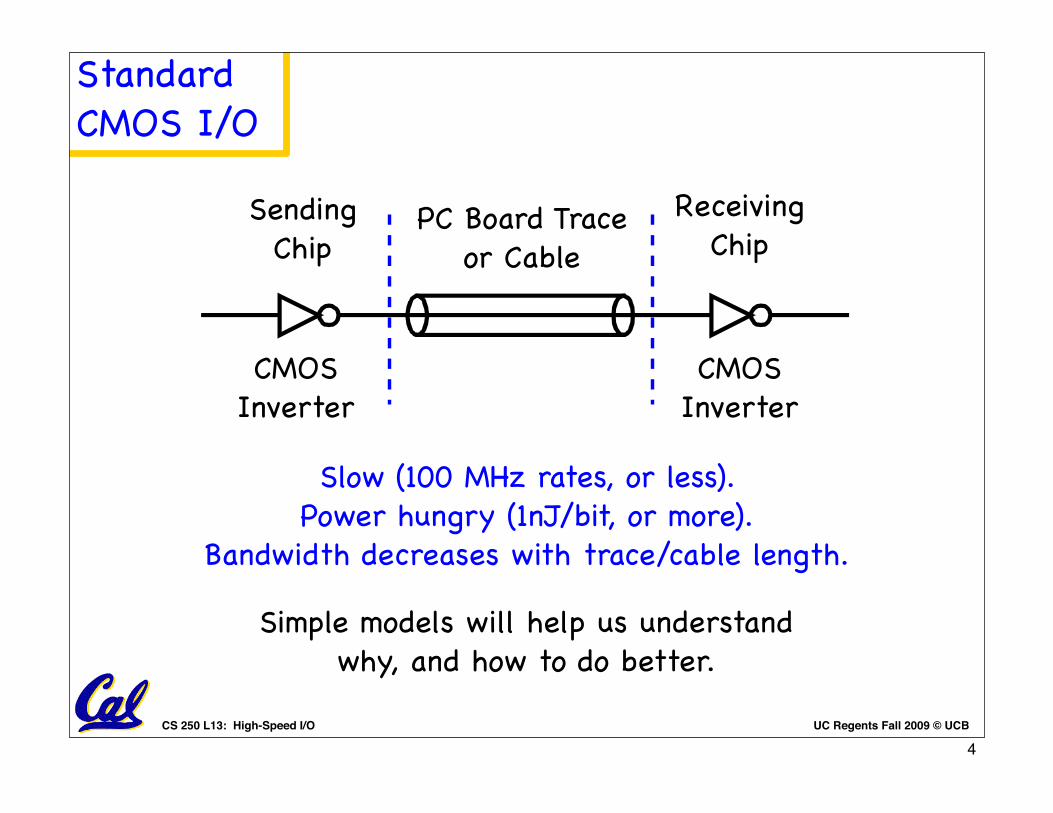
The traditional CMOS system is slow because the high
impedance driver is unable to switch the line on the inci-
dent wave. Instead, the driver must ring up the line as the
signal propagates over several round-trips of the line as
shown in Figure 2. The figure shows the voltage as a frac-
tion of VDD at the far end of the line as a function of time.
The incident wave only switches the line to 10% of VDD.
This is doubled by the first reflection at 10ns. Seven tra-
versals of the 4ns line are required to ring the line up to
50% of VDD, and over 15 traversals are needed for the line
to converge to within 10% of its final value.
Figure 2: An 8mA CMOS Driver rings up a 4ns line termi-
nated into 1K!.
The traditional CMOS system is power hungry, dissipat-
ing 1nJ or more to transmit each bit because it requires
large signal swings to overcome poor noise isolation. The
system uses noisy power supplies as transmit and receive
voltage references. It also uses a CMOS inverter which
has both a large offset voltage across process corners (typi-
cally 300mV) and poor sensitivity (about 500mV) as a
receiver. To overcome these noise sources, a large signal
swing, typically the full power supply, is required.
2.2 Low-Swing, Incident-Wave Signaling
A signaling system that overcomes the limitations of
traditional CMOS signaling is shown in Figure 2. A cur-
rent-source transmitter drives the line. A typical drive is
±5mA which gives a 250mV signal swing. The line is ter-
minated at both ends into its characteristic impedance. The
receiver termination absorbs the incident wave preventing
any reflections. The source termination makes the system
more tolerant of crosstalk and impedance discontinuities
by absorbing any ‘stray’ waves that arrive back at the
source. A high-gain clocked regenerative receive amplifier
gives low offset (typically 10mV) and good sensitivity
(10mV or better depending on settling time).
Figure 2: A low-swing, incident-wave signaling system.
By operating using only the incident wave, the system
of Figure 2 can operate at a data rate independent of the
length of the line. A new bit can be driven onto the source
end of the line before the previous bit arrives at the
receiver. As discussed below, this results in a data rate
that, to first approximation, scales linearly with device
speed.
This system operates reliably using a very small voltage
swing (250mV) because it isolates the signal from many
noise sources. Transmit and receive references are isolated
from the noisy power supplies and a clocked receive ampli-
fier greatly improves offset and sensitivity.
3. Limitations on Signaling Rate
The data rate of a signaling system is limited by both the
electronics used to generate and receive the signal and the
medium over which the signal propagates.
3.1 Electronic Limits on Signaling Rate
As illustrated in Figure 3, electronics limits signaling
rate due to rise-time, aperture time, and timing uncertainty
[DP98b]. The time for a bit cell, tbit, must be made long
enough for the signal to slew from one logic level to
another, tr, for the receiver to sample this signal while sta-
ble, ta, and to tolerate jitter between the signal and the sam-
pling clock, 2tu.
All three of these factors are related to the basic time
constant of the semiconductor technology,"n, the time for a
minimum-sized nFET to discharge the gate of an equal-
sized nFET [DP98b]. This time constant is given approxi-
mately by
. (1)
RO= 400! Z0= 50! A=6
0
0.2
0.4
0.6
0.8
0 20 40 60 80
Time (nsec)
Z0= 50!
RO= 50!
+
–
RT= 50!
+/-5mA
"n
VDDCg
IDSS
-----------------=
Standard CMOS I/O
Sending Chip
Receiving Chip
PC Board Trace or Cable
CMOS Inverter
CMOS Inverter
Slow (100 MHz rates, or less). Power hungry (1nJ/bit, or more).
Bandwidth decreases with trace/cable length.
Simple models will help us understand why, and how to do better.
4
UC Regents Fall 2009 © UCBCS 250 L13: High-Speed I/O
modern microprocessors operate their external buses at
small fraction of their internal clock rate.
Figure 1: A traditional CMOS signaling system.
Figure 1 shows a traditional CMOS signaling system.
CMOS inverters are used as both driver and receiver. The
transmission medium, typically a cable or PC-board trace
has a characteristic impedance of about 50!. The driver
typically has an output impedance of 400! and the line is
unterminated at the receiver. The two power supplies
(VDD = 3.3V and GND = 0V) are used to represent logic 1
and 0 respectively.
The traditional CMOS system is slow because the high
impedance driver is unable to switch the line on the inci-
dent wave. Instead, the driver must ring up the line as the
signal propagates over several round-trips of the line as
shown in Figure 2. The figure shows the voltage as a frac-
tion of VDD at the far end of the line as a function of time.
The incident wave only switches the line to 10% of VDD.
This is doubled by the first reflection at 10ns. Seven tra-
versals of the 4ns line are required to ring the line up to
50% of VDD, and over 15 traversals are needed for the line
to converge to within 10% of its final value.
Figure 2: An 8mA CMOS Driver rings up a 4ns line termi-
nated into 1K!.
The traditional CMOS system is power hungry, dissipat-
ing 1nJ or more to transmit each bit because it requires
large signal swings to overcome poor noise isolation. The
system uses noisy power supplies as transmit and receive
voltage references. It also uses a CMOS inverter which
has both a large offset voltage across process corners (typi-
cally 300mV) and poor sensitivity (about 500mV) as a
receiver. To overcome these noise sources, a large signal
swing, typically the full power supply, is required.
2.2 Low-Swing, Incident-Wave Signaling
A signaling system that overcomes the limitations of
traditional CMOS signaling is shown in Figure 2. A cur-
rent-source transmitter drives the line. A typical drive is
±5mA which gives a 250mV signal swing. The line is ter-
minated at both ends into its characteristic impedance. The
receiver termination absorbs the incident wave preventing
any reflections. The source termination makes the system
more tolerant of crosstalk and impedance discontinuities
by absorbing any ‘stray’ waves that arrive back at the
source. A high-gain clocked regenerative receive amplifier
gives low offset (typically 10mV) and good sensitivity
(10mV or better depending on settling time).
Figure 2: A low-swing, incident-wave signaling system.
By operating using only the incident wave, the system
of Figure 2 can operate at a data rate independent of the
length of the line. A new bit can be driven onto the source
end of the line before the previous bit arrives at the
receiver. As discussed below, this results in a data rate
that, to first approximation, scales linearly with device
speed.
This system operates reliably using a very small voltage
swing (250mV) because it isolates the signal from many
noise sources. Transmit and receive references are isolated
from the noisy power supplies and a clocked receive ampli-
fier greatly improves offset and sensitivity.
3. Limitations on Signaling Rate
The data rate of a signaling system is limited by both the
electronics used to generate and receive the signal and the
medium over which the signal propagates.
3.1 Electronic Limits on Signaling Rate
As illustrated in Figure 3, electronics limits signaling
rate due to rise-time, aperture time, and timing uncertainty
[DP98b]. The time for a bit cell, tbit, must be made long
enough for the signal to slew from one logic level to
another, tr, for the receiver to sample this signal while sta-
ble, ta, and to tolerate jitter between the signal and the sam-
pling clock, 2tu.
All three of these factors are related to the basic time
constant of the semiconductor technology,"n, the time for a
minimum-sized nFET to discharge the gate of an equal-
sized nFET [DP98b]. This time constant is given approxi-
mately by
. (1)
RO= 400! Z0= 50! A=6
0
0.2
0.4
0.6
0.8
0 20 40 60 80
Time (nsec)
Z0= 50!
RO= 50!
+
–
RT= 50!
+/-5mA
"n
VDDCg
IDSS
-----------------=
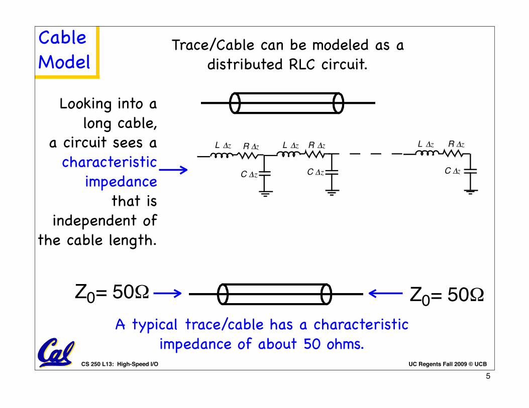
Cable Model
Trace/Cable can be modeled as a distributed RLC circuit.of the transition time of the signal at the input of a CMOS gate
driving an interconnect line to the time of flight of a wave across
the interconnect is a second useful figure of merit to determine the
relative importance of inductance to a specific line.
A. Damping Factor
R !zL !z
C !z
R !zL !z
C !z
z
R !zL !z
C !z
Fig. 1. RLC transmission line model of an interconnect line.
A single interconnect line can be modeled as an RLC
transmission line as shown in Fig. 1, where R, L, and C are the
resistance, inductance, and capacitance per unit length,
respectively, and !z is an incremental length segment of the line.
For an RLC transmission line driven by a sinusoidal input Re{ej"t},
the voltage across the transmission line [11] is
V z t V e V ej t z j t z
( , ) Re{ }( ) ( )
= +! +
1 2" # " #
. (1)
The solution of V(z,t) is the sum of two traveling waves, one in the
positive z direction and the other in the negative z direction. V1 i s
the summation of the original voltage wave and all the reflected
voltage waves in the positive z direction. V2 is the summation of
all the reflected voltage waves traveling in the negative z
direction. The propagation constant of the transmission line, #,
describes the characteristics of the wave propagation across the
line. For an RLC transmission line, the propagation constant i s
complex [11] and is
# $ %= + j , (2)
where the real part $ is the attenuation constant of the waves as the
waves propagate across the line, and the imaginary part % is the
phase constant which determines the speed of propagation of the
waves across the line. Substituting (2) into (1), the real part of the
voltage is given by
V z t V e t z V e t zz z( , ) cos( ) cos( )= ! + +
!1 2
$ $" % " % . (3)
The attenuation of a traveling wave is exponentially dependent on
the distance traveled by the wave, and both the attenuation and
speed of the wave are frequency dependent.
The speed of propagation of the wave across the line [11] is
v ="
%. (4)
The sequence of events that constitutes a transient response for an
input wave begins with a portion of the wave launched into the
line from the source end. This wave propagates across the line
towards the load with a speed determined by (4). The wave
attenuates as it travels across the lossy line. If a mismatch exists
between the characteristic impedance of the transmission line and
the load impedance, a reflected wave is generated and propagates
towards the source to compensate for the mismatch. This reflected
wave is further attenuated as it moves towards the source. The
reflection process is repeated infinitely, but practically, the signal
can be considered to be at steady state when the reflections become
negligible. As the rate of attenuation increases, the reflections
become negligible faster. This behavior can be explained by
noting that the waves are multiplied by a factor of e-2$l for a round
trip across the line, where l is the length of the line. This aspect
means that as the line becomes longer, the effect of the reflections
becomes less and the line behaves as an RC line. This same
behavior occurs if the resistance of the line increases, increasing
the attenuation constant. The attenuation constant $ of an RLC
transmission line can be derived from the basic equations and is
$ ""
= + !LCR
L
1
21 1
2( ( ( ) ) ) . (5)
The attenuation constant as a function of frequency is plotted
in Fig. 2 with L=10-8 H/cm, R=400 &/cm, and C=10-12 F/cm [12].
The attenuation constant is shown to saturate with increasing
frequency to an asymptotic value given by
$asymR C
L=2
, (6)
and the radial frequency at which this saturation begins is given by
"asymR
L& . (7)
This analysis of an RLC transmission line is compared to the
analysis of a lumped RLC circuit (see Fig. 3 for a lumped RLC
circuit). The interconnect is modeled as a single section RLC
circuit with Rt=Rl, Lt=Ll, and Ct=Cl. The poles of this circuit are
p1 2 021, [ ( )]= ! ± !" ' ' , (8)
and the damping factor ' is
' $= =Rl C
Ll asym
2. (9)
As (8) implies, if ' is greater than one, the poles are real and the
effect of the inductance on the circuit is small. The greater the
value of ', the more accurate the RC model becomes. On the other
hand, as ' becomes less than one, the poles become complex and
oscillations occur. In that case, the inductance cannot be
Fig. 2. The attenuation constant $ versus the radial frequency ".
C
RLt t
t
+
-
+
-
Vin
Vout
Fig. 3. Simple lumped RLC circuit model of an
interconnect line.
$0asym
"asym
Attenuation$
Radial Frequency " (Hz)
Looking into a long cable,
a circuit sees a characteristic
impedance that is
independent of the cable length.
modern microprocessors operate their external buses at
small fraction of their internal clock rate.
Figure 1: A traditional CMOS signaling system.
Figure 1 shows a traditional CMOS signaling system.
CMOS inverters are used as both driver and receiver. The
transmission medium, typically a cable or PC-board trace
has a characteristic impedance of about 50!. The driver
typically has an output impedance of 400! and the line is
unterminated at the receiver. The two power supplies
(VDD = 3.3V and GND = 0V) are used to represent logic 1
and 0 respectively.
The traditional CMOS system is slow because the high
impedance driver is unable to switch the line on the inci-
dent wave. Instead, the driver must ring up the line as the
signal propagates over several round-trips of the line as
shown in Figure 2. The figure shows the voltage as a frac-
tion of VDD at the far end of the line as a function of time.
The incident wave only switches the line to 10% of VDD.
This is doubled by the first reflection at 10ns. Seven tra-
versals of the 4ns line are required to ring the line up to
50% of VDD, and over 15 traversals are needed for the line
to converge to within 10% of its final value.
Figure 2: An 8mA CMOS Driver rings up a 4ns line termi-
nated into 1K!.
The traditional CMOS system is power hungry, dissipat-
ing 1nJ or more to transmit each bit because it requires
large signal swings to overcome poor noise isolation. The
system uses noisy power supplies as transmit and receive
voltage references. It also uses a CMOS inverter which
has both a large offset voltage across process corners (typi-
cally 300mV) and poor sensitivity (about 500mV) as a
receiver. To overcome these noise sources, a large signal
swing, typically the full power supply, is required.
2.2 Low-Swing, Incident-Wave Signaling
A signaling system that overcomes the limitations of
traditional CMOS signaling is shown in Figure 2. A cur-
rent-source transmitter drives the line. A typical drive is
±5mA which gives a 250mV signal swing. The line is ter-
minated at both ends into its characteristic impedance. The
receiver termination absorbs the incident wave preventing
any reflections. The source termination makes the system
more tolerant of crosstalk and impedance discontinuities
by absorbing any ‘stray’ waves that arrive back at the
source. A high-gain clocked regenerative receive amplifier
gives low offset (typically 10mV) and good sensitivity
(10mV or better depending on settling time).
Figure 2: A low-swing, incident-wave signaling system.
By operating using only the incident wave, the system
of Figure 2 can operate at a data rate independent of the
length of the line. A new bit can be driven onto the source
end of the line before the previous bit arrives at the
receiver. As discussed below, this results in a data rate
that, to first approximation, scales linearly with device
speed.
This system operates reliably using a very small voltage
swing (250mV) because it isolates the signal from many
noise sources. Transmit and receive references are isolated
from the noisy power supplies and a clocked receive ampli-
fier greatly improves offset and sensitivity.
3. Limitations on Signaling Rate
The data rate of a signaling system is limited by both the
electronics used to generate and receive the signal and the
medium over which the signal propagates.
3.1 Electronic Limits on Signaling Rate
As illustrated in Figure 3, electronics limits signaling
rate due to rise-time, aperture time, and timing uncertainty
[DP98b]. The time for a bit cell, tbit, must be made long
enough for the signal to slew from one logic level to
another, tr, for the receiver to sample this signal while sta-
ble, ta, and to tolerate jitter between the signal and the sam-
pling clock, 2tu.
All three of these factors are related to the basic time
constant of the semiconductor technology,"n, the time for a
minimum-sized nFET to discharge the gate of an equal-
sized nFET [DP98b]. This time constant is given approxi-
mately by
. (1)
RO= 400! Z0= 50! A=6
0
0.2
0.4
0.6
0.8
0 20 40 60 80
Time (nsec)
Z0= 50!
RO= 50!
+
–
RT= 50!
+/-5mA
"n
VDDCg
IDSS
-----------------=
A typical trace/cable has a characteristic impedance of about 50 ohms.
5

UC Regents Fall 2009 © UCBCS 250 L13: High-Speed I/O
modern microprocessors operate their external buses at
small fraction of their internal clock rate.
Figure 1: A traditional CMOS signaling system.
Figure 1 shows a traditional CMOS signaling system.
CMOS inverters are used as both driver and receiver. The
transmission medium, typically a cable or PC-board trace
has a characteristic impedance of about 50!. The driver
typically has an output impedance of 400! and the line is
unterminated at the receiver. The two power supplies
(VDD = 3.3V and GND = 0V) are used to represent logic 1
and 0 respectively.
The traditional CMOS system is slow because the high
impedance driver is unable to switch the line on the inci-
dent wave. Instead, the driver must ring up the line as the
signal propagates over several round-trips of the line as
shown in Figure 2. The figure shows the voltage as a frac-
tion of VDD at the far end of the line as a function of time.
The incident wave only switches the line to 10% of VDD.
This is doubled by the first reflection at 10ns. Seven tra-
versals of the 4ns line are required to ring the line up to
50% of VDD, and over 15 traversals are needed for the line
to converge to within 10% of its final value.
Figure 2: An 8mA CMOS Driver rings up a 4ns line termi-
nated into 1K!.
The traditional CMOS system is power hungry, dissipat-
ing 1nJ or more to transmit each bit because it requires
large signal swings to overcome poor noise isolation. The
system uses noisy power supplies as transmit and receive
voltage references. It also uses a CMOS inverter which
has both a large offset voltage across process corners (typi-
cally 300mV) and poor sensitivity (about 500mV) as a
receiver. To overcome these noise sources, a large signal
swing, typically the full power supply, is required.
2.2 Low-Swing, Incident-Wave Signaling
A signaling system that overcomes the limitations of
traditional CMOS signaling is shown in Figure 2. A cur-
rent-source transmitter drives the line. A typical drive is
±5mA which gives a 250mV signal swing. The line is ter-
minated at both ends into its characteristic impedance. The
receiver termination absorbs the incident wave preventing
any reflections. The source termination makes the system
more tolerant of crosstalk and impedance discontinuities
by absorbing any ‘stray’ waves that arrive back at the
source. A high-gain clocked regenerative receive amplifier
gives low offset (typically 10mV) and good sensitivity
(10mV or better depending on settling time).
Figure 2: A low-swing, incident-wave signaling system.
By operating using only the incident wave, the system
of Figure 2 can operate at a data rate independent of the
length of the line. A new bit can be driven onto the source
end of the line before the previous bit arrives at the
receiver. As discussed below, this results in a data rate
that, to first approximation, scales linearly with device
speed.
This system operates reliably using a very small voltage
swing (250mV) because it isolates the signal from many
noise sources. Transmit and receive references are isolated
from the noisy power supplies and a clocked receive ampli-
fier greatly improves offset and sensitivity.
3. Limitations on Signaling Rate
The data rate of a signaling system is limited by both the
electronics used to generate and receive the signal and the
medium over which the signal propagates.
3.1 Electronic Limits on Signaling Rate
As illustrated in Figure 3, electronics limits signaling
rate due to rise-time, aperture time, and timing uncertainty
[DP98b]. The time for a bit cell, tbit, must be made long
enough for the signal to slew from one logic level to
another, tr, for the receiver to sample this signal while sta-
ble, ta, and to tolerate jitter between the signal and the sam-
pling clock, 2tu.
All three of these factors are related to the basic time
constant of the semiconductor technology,"n, the time for a
minimum-sized nFET to discharge the gate of an equal-
sized nFET [DP98b]. This time constant is given approxi-
mately by
. (1)
RO= 400! Z0= 50! A=6
0
0.2
0.4
0.6
0.8
0 20 40 60 80
Time (nsec)
Z0= 50!
RO= 50!
+
–
RT= 50!
+/-5mA
"n
VDDCg
IDSS
-----------------=
Cable Model
IEEE JOURNAL OF SOLID-STATE CIRCUITS, VOL. 38, NO. 5, MAY 2003 835
TABLE IDIFFERENT FREQUENCY REGIMES OF PROPAGATION
per unit length, respectively. This intuitively suggests that at
lower frequencies, the first term on the right side of (1) dom-
inates, and the wire behaves as a distributed network. In
this regime, signals travel slowly by diffusion and undergo
frequency dispersion. As the frequency increases, the inductive
component of the wire [second term on the right side of (1)]
begins to dominate over the resistance, and the wire behaves
more as a waveguide. The high-frequency regime allows for
propagation of an electromagnetic wave; consequently, the peak
phase velocity is the speed of light in the dielectric surrounding
the interconnect (Table I). This is the key characteristic of the
wire that can be exploited in order to achieve high-speed signal
propagation. Fig. 3 shows the experimental velocity and atten-
uation characteristics of an on-chip 1-mm-long coplanar wave-
guide, with 4.8- m-wide signal, 20- m groundwires, and 5- m
spacing, which is obtained through -parameter measurements
[6].
In the example given in Fig. 2, most of the spectral com-
ponents of the 500-ps pulse are in the regime of the min-
imum-sized wire, traveling at speeds much less than the speed
of light. It is not until over 100 GHz that the velocity reaches its
maximum and becomes independent of frequency. The effect
on digital signals is that different frequency components travel
at different speeds and attenuate at different levels, resulting
in a significantly distorted output. Repeater insertion does not
change the frequency characteristics of the interconnect, but can
improve speed by amplifying the faster high-frequency compo-
nents of the signal, when placed at appropriate intervals. This
comes at the cost of increased power dissipation and a delay
overhead from the intrinsic delay of the repeater.
III. EXPLOITING THE LC NATURE OF WIRES
The characteristics shown in Fig. 3 suggest that a high-speed
system can be built by taking advantage of the wave nature of
interconnect. At the same time, it is beneficial to eliminate the
low-frequency portion of the signal that lags behind and con-
tributes to inter-symbol interference (ISI). This can be achieved
bymodulating the digital data with a sufficiently high-frequency
carrier, and as a result, concentrating all of the signal power in
the faster regime.
In order for this system to be realizable, wires must have a
low crossover frequency between the and regimes. By
explicitly emphasizing the parasitic inductance and reducing the
resistance, this transition can be shifted into the single-gigahertz
range. This design strategy of deliberately using the parasitic
inductance may be foreign to designers, since the inductance
for on-chip wires is often difficult to estimate. In this case, the
Fig. 3. Experimental results showing velocity and attenuation as a function offrequency for a 1-mm-long coplanar waveguide.
Fig. 4. Frequency characteristics of modulated pulse and low-loss on-chipinterconnect. is the speed of light in silicon dioxide.
on-chip transmission lines used have explicit ground returns that
provide well-controlled and predictable inductance values.
While the high-frequency regime offers high-speed
frequency-dispersionless propagation, the interconnect is
substantially more lossy at higher frequencies, as demonstrated
by Fig. 3. Therefore, the wire must be optimized to minimize
loss, while occupying a reasonable amount of area. Thicker
top layers of metal and dielectric facilitate the realization of
on-chip transmission lines [7], [8]. For example, a microstrip
structure with a 6- m-wide 2- m-thick copper signal wire on
a 2- m-thick dielectric provides a loss of about 0.5 dB/mm
[6]. This totals 10–15-dB loss for a cross-chip global wire.
This amount of attenuation is tolerable for a system to reliably
recover the signal. In this case, no gain elements, such as
repeaters or amplifiers, are present or necessary along the
length of interconnect.
Fig. 4 shows the impact of using modulated signaling in com-
bination with the use of low-loss interconnect. Using optimized
interconnect lowers the crossover frequency between the
and regimes to a few gigahertz. Using a high-frequency car-
rier pushes the signal spectral components to lie predominately
in the high-speed inductance-dominated region.
IV. SYSTEM IMPLEMENTATION
A simple implementation of this system uses direct conver-
sion from baseband to RF, as illustrated in Fig. 5. The carrier
The highest frequencies of a pulse edge on a wire travel approach the
“speed of light” of the wire medium (cw).
Wire of length “L”And so, the fast rising edge of a pulse takes about L/cw seconds to traverse a wire of length L.
For our example, assume L/cw = 4ns.
6
UC Regents Fall 2009 © UCBCS 250 L13: High-Speed I/O
modern microprocessors operate their external buses at
small fraction of their internal clock rate.
Figure 1: A traditional CMOS signaling system.
Figure 1 shows a traditional CMOS signaling system.
CMOS inverters are used as both driver and receiver. The
transmission medium, typically a cable or PC-board trace
has a characteristic impedance of about 50!. The driver
typically has an output impedance of 400! and the line is
unterminated at the receiver. The two power supplies
(VDD = 3.3V and GND = 0V) are used to represent logic 1
and 0 respectively.
The traditional CMOS system is slow because the high
impedance driver is unable to switch the line on the inci-
dent wave. Instead, the driver must ring up the line as the
signal propagates over several round-trips of the line as
shown in Figure 2. The figure shows the voltage as a frac-
tion of VDD at the far end of the line as a function of time.
The incident wave only switches the line to 10% of VDD.
This is doubled by the first reflection at 10ns. Seven tra-
versals of the 4ns line are required to ring the line up to
50% of VDD, and over 15 traversals are needed for the line
to converge to within 10% of its final value.
Figure 2: An 8mA CMOS Driver rings up a 4ns line termi-
nated into 1K!.
The traditional CMOS system is power hungry, dissipat-
ing 1nJ or more to transmit each bit because it requires
large signal swings to overcome poor noise isolation. The
system uses noisy power supplies as transmit and receive
voltage references. It also uses a CMOS inverter which
has both a large offset voltage across process corners (typi-
cally 300mV) and poor sensitivity (about 500mV) as a
receiver. To overcome these noise sources, a large signal
swing, typically the full power supply, is required.
2.2 Low-Swing, Incident-Wave Signaling
A signaling system that overcomes the limitations of
traditional CMOS signaling is shown in Figure 2. A cur-
rent-source transmitter drives the line. A typical drive is
±5mA which gives a 250mV signal swing. The line is ter-
minated at both ends into its characteristic impedance. The
receiver termination absorbs the incident wave preventing
any reflections. The source termination makes the system
more tolerant of crosstalk and impedance discontinuities
by absorbing any ‘stray’ waves that arrive back at the
source. A high-gain clocked regenerative receive amplifier
gives low offset (typically 10mV) and good sensitivity
(10mV or better depending on settling time).
Figure 2: A low-swing, incident-wave signaling system.
By operating using only the incident wave, the system
of Figure 2 can operate at a data rate independent of the
length of the line. A new bit can be driven onto the source
end of the line before the previous bit arrives at the
receiver. As discussed below, this results in a data rate
that, to first approximation, scales linearly with device
speed.
This system operates reliably using a very small voltage
swing (250mV) because it isolates the signal from many
noise sources. Transmit and receive references are isolated
from the noisy power supplies and a clocked receive ampli-
fier greatly improves offset and sensitivity.
3. Limitations on Signaling Rate
The data rate of a signaling system is limited by both the
electronics used to generate and receive the signal and the
medium over which the signal propagates.
3.1 Electronic Limits on Signaling Rate
As illustrated in Figure 3, electronics limits signaling
rate due to rise-time, aperture time, and timing uncertainty
[DP98b]. The time for a bit cell, tbit, must be made long
enough for the signal to slew from one logic level to
another, tr, for the receiver to sample this signal while sta-
ble, ta, and to tolerate jitter between the signal and the sam-
pling clock, 2tu.
All three of these factors are related to the basic time
constant of the semiconductor technology,"n, the time for a
minimum-sized nFET to discharge the gate of an equal-
sized nFET [DP98b]. This time constant is given approxi-
mately by
. (1)
RO= 400! Z0= 50! A=6
0
0.2
0.4
0.6
0.8
0 20 40 60 80
Time (nsec)
Z0= 50!
RO= 50!
+
–
RT= 50!
+/-5mA
"n
VDDCg
IDSS
-----------------=
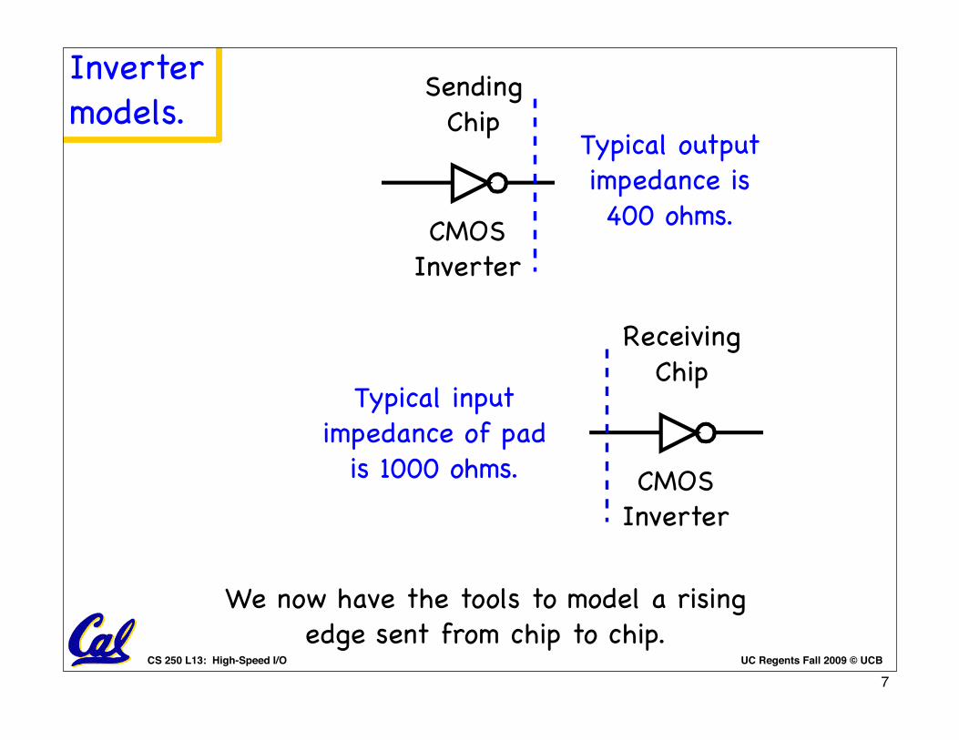
Inverter models.
Sending Chip
CMOS Inverter
Typical output impedance is 400 ohms.
modern microprocessors operate their external buses at
small fraction of their internal clock rate.
Figure 1: A traditional CMOS signaling system.
Figure 1 shows a traditional CMOS signaling system.
CMOS inverters are used as both driver and receiver. The
transmission medium, typically a cable or PC-board trace
has a characteristic impedance of about 50!. The driver
typically has an output impedance of 400! and the line is
unterminated at the receiver. The two power supplies
(VDD = 3.3V and GND = 0V) are used to represent logic 1
and 0 respectively.
The traditional CMOS system is slow because the high
impedance driver is unable to switch the line on the inci-
dent wave. Instead, the driver must ring up the line as the
signal propagates over several round-trips of the line as
shown in Figure 2. The figure shows the voltage as a frac-
tion of VDD at the far end of the line as a function of time.
The incident wave only switches the line to 10% of VDD.
This is doubled by the first reflection at 10ns. Seven tra-
versals of the 4ns line are required to ring the line up to
50% of VDD, and over 15 traversals are needed for the line
to converge to within 10% of its final value.
Figure 2: An 8mA CMOS Driver rings up a 4ns line termi-
nated into 1K!.
The traditional CMOS system is power hungry, dissipat-
ing 1nJ or more to transmit each bit because it requires
large signal swings to overcome poor noise isolation. The
system uses noisy power supplies as transmit and receive
voltage references. It also uses a CMOS inverter which
has both a large offset voltage across process corners (typi-
cally 300mV) and poor sensitivity (about 500mV) as a
receiver. To overcome these noise sources, a large signal
swing, typically the full power supply, is required.
2.2 Low-Swing, Incident-Wave Signaling
A signaling system that overcomes the limitations of
traditional CMOS signaling is shown in Figure 2. A cur-
rent-source transmitter drives the line. A typical drive is
±5mA which gives a 250mV signal swing. The line is ter-
minated at both ends into its characteristic impedance. The
receiver termination absorbs the incident wave preventing
any reflections. The source termination makes the system
more tolerant of crosstalk and impedance discontinuities
by absorbing any ‘stray’ waves that arrive back at the
source. A high-gain clocked regenerative receive amplifier
gives low offset (typically 10mV) and good sensitivity
(10mV or better depending on settling time).
Figure 2: A low-swing, incident-wave signaling system.
By operating using only the incident wave, the system
of Figure 2 can operate at a data rate independent of the
length of the line. A new bit can be driven onto the source
end of the line before the previous bit arrives at the
receiver. As discussed below, this results in a data rate
that, to first approximation, scales linearly with device
speed.
This system operates reliably using a very small voltage
swing (250mV) because it isolates the signal from many
noise sources. Transmit and receive references are isolated
from the noisy power supplies and a clocked receive ampli-
fier greatly improves offset and sensitivity.
3. Limitations on Signaling Rate
The data rate of a signaling system is limited by both the
electronics used to generate and receive the signal and the
medium over which the signal propagates.
3.1 Electronic Limits on Signaling Rate
As illustrated in Figure 3, electronics limits signaling
rate due to rise-time, aperture time, and timing uncertainty
[DP98b]. The time for a bit cell, tbit, must be made long
enough for the signal to slew from one logic level to
another, tr, for the receiver to sample this signal while sta-
ble, ta, and to tolerate jitter between the signal and the sam-
pling clock, 2tu.
All three of these factors are related to the basic time
constant of the semiconductor technology,"n, the time for a
minimum-sized nFET to discharge the gate of an equal-
sized nFET [DP98b]. This time constant is given approxi-
mately by
. (1)
RO= 400! Z0= 50! A=6
0
0.2
0.4
0.6
0.8
0 20 40 60 80
Time (nsec)
Z0= 50!
RO= 50!
+
–
RT= 50!
+/-5mA
"n
VDDCg
IDSS
-----------------=
Receiving Chip
CMOS Inverter
Typical input impedance of pad
is 1000 ohms.
We now have the tools to model a rising edge sent from chip to chip.
7

UC Regents Fall 2009 © UCBCS 250 L13: High-Speed I/O
modern microprocessors operate their external buses at
small fraction of their internal clock rate.
Figure 1: A traditional CMOS signaling system.
Figure 1 shows a traditional CMOS signaling system.
CMOS inverters are used as both driver and receiver. The
transmission medium, typically a cable or PC-board trace
has a characteristic impedance of about 50!. The driver
typically has an output impedance of 400! and the line is
unterminated at the receiver. The two power supplies
(VDD = 3.3V and GND = 0V) are used to represent logic 1
and 0 respectively.
The traditional CMOS system is slow because the high
impedance driver is unable to switch the line on the inci-
dent wave. Instead, the driver must ring up the line as the
signal propagates over several round-trips of the line as
shown in Figure 2. The figure shows the voltage as a frac-
tion of VDD at the far end of the line as a function of time.
The incident wave only switches the line to 10% of VDD.
This is doubled by the first reflection at 10ns. Seven tra-
versals of the 4ns line are required to ring the line up to
50% of VDD, and over 15 traversals are needed for the line
to converge to within 10% of its final value.
Figure 2: An 8mA CMOS Driver rings up a 4ns line termi-
nated into 1K!.
The traditional CMOS system is power hungry, dissipat-
ing 1nJ or more to transmit each bit because it requires
large signal swings to overcome poor noise isolation. The
system uses noisy power supplies as transmit and receive
voltage references. It also uses a CMOS inverter which
has both a large offset voltage across process corners (typi-
cally 300mV) and poor sensitivity (about 500mV) as a
receiver. To overcome these noise sources, a large signal
swing, typically the full power supply, is required.
2.2 Low-Swing, Incident-Wave Signaling
A signaling system that overcomes the limitations of
traditional CMOS signaling is shown in Figure 2. A cur-
rent-source transmitter drives the line. A typical drive is
±5mA which gives a 250mV signal swing. The line is ter-
minated at both ends into its characteristic impedance. The
receiver termination absorbs the incident wave preventing
any reflections. The source termination makes the system
more tolerant of crosstalk and impedance discontinuities
by absorbing any ‘stray’ waves that arrive back at the
source. A high-gain clocked regenerative receive amplifier
gives low offset (typically 10mV) and good sensitivity
(10mV or better depending on settling time).
Figure 2: A low-swing, incident-wave signaling system.
By operating using only the incident wave, the system
of Figure 2 can operate at a data rate independent of the
length of the line. A new bit can be driven onto the source
end of the line before the previous bit arrives at the
receiver. As discussed below, this results in a data rate
that, to first approximation, scales linearly with device
speed.
This system operates reliably using a very small voltage
swing (250mV) because it isolates the signal from many
noise sources. Transmit and receive references are isolated
from the noisy power supplies and a clocked receive ampli-
fier greatly improves offset and sensitivity.
3. Limitations on Signaling Rate
The data rate of a signaling system is limited by both the
electronics used to generate and receive the signal and the
medium over which the signal propagates.
3.1 Electronic Limits on Signaling Rate
As illustrated in Figure 3, electronics limits signaling
rate due to rise-time, aperture time, and timing uncertainty
[DP98b]. The time for a bit cell, tbit, must be made long
enough for the signal to slew from one logic level to
another, tr, for the receiver to sample this signal while sta-
ble, ta, and to tolerate jitter between the signal and the sam-
pling clock, 2tu.
All three of these factors are related to the basic time
constant of the semiconductor technology,"n, the time for a
minimum-sized nFET to discharge the gate of an equal-
sized nFET [DP98b]. This time constant is given approxi-
mately by
. (1)
RO= 400! Z0= 50! A=6
0
0.2
0.4
0.6
0.8
0 20 40 60 80
Time (nsec)
Z0= 50!
RO= 50!
+
–
RT= 50!
+/-5mA
"n
VDDCg
IDSS
-----------------=
Standard CMOS I/O
400 ohm output
impedance
1000 ohm input
impedance
50 ohm characteristic impedance
4ns flight time
VrVs
modern microprocessors operate their external buses at
small fraction of their internal clock rate.
Figure 1: A traditional CMOS signaling system.
Figure 1 shows a traditional CMOS signaling system.
CMOS inverters are used as both driver and receiver. The
transmission medium, typically a cable or PC-board trace
has a characteristic impedance of about 50!. The driver
typically has an output impedance of 400! and the line is
unterminated at the receiver. The two power supplies
(VDD = 3.3V and GND = 0V) are used to represent logic 1
and 0 respectively.
The traditional CMOS system is slow because the high
impedance driver is unable to switch the line on the inci-
dent wave. Instead, the driver must ring up the line as the
signal propagates over several round-trips of the line as
shown in Figure 2. The figure shows the voltage as a frac-
tion of VDD at the far end of the line as a function of time.
The incident wave only switches the line to 10% of VDD.
This is doubled by the first reflection at 10ns. Seven tra-
versals of the 4ns line are required to ring the line up to
50% of VDD, and over 15 traversals are needed for the line
to converge to within 10% of its final value.
Figure 2: An 8mA CMOS Driver rings up a 4ns line termi-
nated into 1K!.
The traditional CMOS system is power hungry, dissipat-
ing 1nJ or more to transmit each bit because it requires
large signal swings to overcome poor noise isolation. The
system uses noisy power supplies as transmit and receive
voltage references. It also uses a CMOS inverter which
has both a large offset voltage across process corners (typi-
cally 300mV) and poor sensitivity (about 500mV) as a
receiver. To overcome these noise sources, a large signal
swing, typically the full power supply, is required.
2.2 Low-Swing, Incident-Wave Signaling
A signaling system that overcomes the limitations of
traditional CMOS signaling is shown in Figure 2. A cur-
rent-source transmitter drives the line. A typical drive is
±5mA which gives a 250mV signal swing. The line is ter-
minated at both ends into its characteristic impedance. The
receiver termination absorbs the incident wave preventing
any reflections. The source termination makes the system
more tolerant of crosstalk and impedance discontinuities
by absorbing any ‘stray’ waves that arrive back at the
source. A high-gain clocked regenerative receive amplifier
gives low offset (typically 10mV) and good sensitivity
(10mV or better depending on settling time).
Figure 2: A low-swing, incident-wave signaling system.
By operating using only the incident wave, the system
of Figure 2 can operate at a data rate independent of the
length of the line. A new bit can be driven onto the source
end of the line before the previous bit arrives at the
receiver. As discussed below, this results in a data rate
that, to first approximation, scales linearly with device
speed.
This system operates reliably using a very small voltage
swing (250mV) because it isolates the signal from many
noise sources. Transmit and receive references are isolated
from the noisy power supplies and a clocked receive ampli-
fier greatly improves offset and sensitivity.
3. Limitations on Signaling Rate
The data rate of a signaling system is limited by both the
electronics used to generate and receive the signal and the
medium over which the signal propagates.
3.1 Electronic Limits on Signaling Rate
As illustrated in Figure 3, electronics limits signaling
rate due to rise-time, aperture time, and timing uncertainty
[DP98b]. The time for a bit cell, tbit, must be made long
enough for the signal to slew from one logic level to
another, tr, for the receiver to sample this signal while sta-
ble, ta, and to tolerate jitter between the signal and the sam-
pling clock, 2tu.
All three of these factors are related to the basic time
constant of the semiconductor technology,"n, the time for a
minimum-sized nFET to discharge the gate of an equal-
sized nFET [DP98b]. This time constant is given approxi-
mately by
. (1)
RO= 400! Z0= 50! A=6
0
0.2
0.4
0.6
0.8
0 20 40 60 80
Time (nsec)
Z0= 50!
RO= 50!
+
–
RT= 50!
+/-5mA
"n
VDDCg
IDSS
-----------------=
Vr15 up-and-back traversals are needed to “ring-up” Vr to 90% of Vdd !
The impedance mismatches at each cable end reduce the pulse heights and launch the cyan reflection waves.
8

UC Regents Fall 2009 © UCBCS 250 L13: High-Speed I/O
Incident-Wave Signaling
9

UC Regents Fall 2009 © UCBCS 250 L13: High-Speed I/O
Incident-wave I/O
modern microprocessors operate their external buses at
small fraction of their internal clock rate.
Figure 1: A traditional CMOS signaling system.
Figure 1 shows a traditional CMOS signaling system.
CMOS inverters are used as both driver and receiver. The
transmission medium, typically a cable or PC-board trace
has a characteristic impedance of about 50!. The driver
typically has an output impedance of 400! and the line is
unterminated at the receiver. The two power supplies
(VDD = 3.3V and GND = 0V) are used to represent logic 1
and 0 respectively.
The traditional CMOS system is slow because the high
impedance driver is unable to switch the line on the inci-
dent wave. Instead, the driver must ring up the line as the
signal propagates over several round-trips of the line as
shown in Figure 2. The figure shows the voltage as a frac-
tion of VDD at the far end of the line as a function of time.
The incident wave only switches the line to 10% of VDD.
This is doubled by the first reflection at 10ns. Seven tra-
versals of the 4ns line are required to ring the line up to
50% of VDD, and over 15 traversals are needed for the line
to converge to within 10% of its final value.
Figure 2: An 8mA CMOS Driver rings up a 4ns line termi-
nated into 1K!.
The traditional CMOS system is power hungry, dissipat-
ing 1nJ or more to transmit each bit because it requires
large signal swings to overcome poor noise isolation. The
system uses noisy power supplies as transmit and receive
voltage references. It also uses a CMOS inverter which
has both a large offset voltage across process corners (typi-
cally 300mV) and poor sensitivity (about 500mV) as a
receiver. To overcome these noise sources, a large signal
swing, typically the full power supply, is required.
2.2 Low-Swing, Incident-Wave Signaling
A signaling system that overcomes the limitations of
traditional CMOS signaling is shown in Figure 2. A cur-
rent-source transmitter drives the line. A typical drive is
±5mA which gives a 250mV signal swing. The line is ter-
minated at both ends into its characteristic impedance. The
receiver termination absorbs the incident wave preventing
any reflections. The source termination makes the system
more tolerant of crosstalk and impedance discontinuities
by absorbing any ‘stray’ waves that arrive back at the
source. A high-gain clocked regenerative receive amplifier
gives low offset (typically 10mV) and good sensitivity
(10mV or better depending on settling time).
Figure 2: A low-swing, incident-wave signaling system.
By operating using only the incident wave, the system
of Figure 2 can operate at a data rate independent of the
length of the line. A new bit can be driven onto the source
end of the line before the previous bit arrives at the
receiver. As discussed below, this results in a data rate
that, to first approximation, scales linearly with device
speed.
This system operates reliably using a very small voltage
swing (250mV) because it isolates the signal from many
noise sources. Transmit and receive references are isolated
from the noisy power supplies and a clocked receive ampli-
fier greatly improves offset and sensitivity.
3. Limitations on Signaling Rate
The data rate of a signaling system is limited by both the
electronics used to generate and receive the signal and the
medium over which the signal propagates.
3.1 Electronic Limits on Signaling Rate
As illustrated in Figure 3, electronics limits signaling
rate due to rise-time, aperture time, and timing uncertainty
[DP98b]. The time for a bit cell, tbit, must be made long
enough for the signal to slew from one logic level to
another, tr, for the receiver to sample this signal while sta-
ble, ta, and to tolerate jitter between the signal and the sam-
pling clock, 2tu.
All three of these factors are related to the basic time
constant of the semiconductor technology,"n, the time for a
minimum-sized nFET to discharge the gate of an equal-
sized nFET [DP98b]. This time constant is given approxi-
mately by
. (1)
RO= 400! Z0= 50! A=6
0
0.2
0.4
0.6
0.8
0 20 40 60 80
Time (nsec)
Z0= 50!
RO= 50!
+
–
RT= 50!
+/-5mA
"n
VDDCg
IDSS
-----------------=
4ns flight timeSending Chip
Receiving Chip
Kill reflections by making input and output impedances match the line impedance.
Each bit is communicated by the first arriving wave (the incident wave).
Several bits can be in-flight on the wire at once.
10

UC Regents Fall 2009 © UCBCS 250 L13: High-Speed I/O
Differential, low-voltage.
modern microprocessors operate their external buses at
small fraction of their internal clock rate.
Figure 1: A traditional CMOS signaling system.
Figure 1 shows a traditional CMOS signaling system.
CMOS inverters are used as both driver and receiver. The
transmission medium, typically a cable or PC-board trace
has a characteristic impedance of about 50!. The driver
typically has an output impedance of 400! and the line is
unterminated at the receiver. The two power supplies
(VDD = 3.3V and GND = 0V) are used to represent logic 1
and 0 respectively.
The traditional CMOS system is slow because the high
impedance driver is unable to switch the line on the inci-
dent wave. Instead, the driver must ring up the line as the
signal propagates over several round-trips of the line as
shown in Figure 2. The figure shows the voltage as a frac-
tion of VDD at the far end of the line as a function of time.
The incident wave only switches the line to 10% of VDD.
This is doubled by the first reflection at 10ns. Seven tra-
versals of the 4ns line are required to ring the line up to
50% of VDD, and over 15 traversals are needed for the line
to converge to within 10% of its final value.
Figure 2: An 8mA CMOS Driver rings up a 4ns line termi-
nated into 1K!.
The traditional CMOS system is power hungry, dissipat-
ing 1nJ or more to transmit each bit because it requires
large signal swings to overcome poor noise isolation. The
system uses noisy power supplies as transmit and receive
voltage references. It also uses a CMOS inverter which
has both a large offset voltage across process corners (typi-
cally 300mV) and poor sensitivity (about 500mV) as a
receiver. To overcome these noise sources, a large signal
swing, typically the full power supply, is required.
2.2 Low-Swing, Incident-Wave Signaling
A signaling system that overcomes the limitations of
traditional CMOS signaling is shown in Figure 2. A cur-
rent-source transmitter drives the line. A typical drive is
±5mA which gives a 250mV signal swing. The line is ter-
minated at both ends into its characteristic impedance. The
receiver termination absorbs the incident wave preventing
any reflections. The source termination makes the system
more tolerant of crosstalk and impedance discontinuities
by absorbing any ‘stray’ waves that arrive back at the
source. A high-gain clocked regenerative receive amplifier
gives low offset (typically 10mV) and good sensitivity
(10mV or better depending on settling time).
Figure 2: A low-swing, incident-wave signaling system.
By operating using only the incident wave, the system
of Figure 2 can operate at a data rate independent of the
length of the line. A new bit can be driven onto the source
end of the line before the previous bit arrives at the
receiver. As discussed below, this results in a data rate
that, to first approximation, scales linearly with device
speed.
This system operates reliably using a very small voltage
swing (250mV) because it isolates the signal from many
noise sources. Transmit and receive references are isolated
from the noisy power supplies and a clocked receive ampli-
fier greatly improves offset and sensitivity.
3. Limitations on Signaling Rate
The data rate of a signaling system is limited by both the
electronics used to generate and receive the signal and the
medium over which the signal propagates.
3.1 Electronic Limits on Signaling Rate
As illustrated in Figure 3, electronics limits signaling
rate due to rise-time, aperture time, and timing uncertainty
[DP98b]. The time for a bit cell, tbit, must be made long
enough for the signal to slew from one logic level to
another, tr, for the receiver to sample this signal while sta-
ble, ta, and to tolerate jitter between the signal and the sam-
pling clock, 2tu.
All three of these factors are related to the basic time
constant of the semiconductor technology,"n, the time for a
minimum-sized nFET to discharge the gate of an equal-
sized nFET [DP98b]. This time constant is given approxi-
mately by
. (1)
RO= 400! Z0= 50! A=6
0
0.2
0.4
0.6
0.8
0 20 40 60 80
Time (nsec)
Z0= 50!
RO= 50!
+
–
RT= 50!
+/-5mA
"n
VDDCg
IDSS
-----------------=
4ns flight timeSending Chip
Receiving Chip
Direction of current (+/-) codes one/zero.Magnitude of current sets voltage (V=IR).
Like an SRAM sense amp.
Differential, senses sign of
voltage.Energy dominated by DC power ...
11
UC Regents Fall 2009 © UCBCS 250 L13: High-Speed I/O
Line Equalization
12

UC Regents Fall 2009 © UCBCS 250 L13: High-Speed I/O
Wire attenuation
modern microprocessors operate their external buses at
small fraction of their internal clock rate.
Figure 1: A traditional CMOS signaling system.
Figure 1 shows a traditional CMOS signaling system.
CMOS inverters are used as both driver and receiver. The
transmission medium, typically a cable or PC-board trace
has a characteristic impedance of about 50!. The driver
typically has an output impedance of 400! and the line is
unterminated at the receiver. The two power supplies
(VDD = 3.3V and GND = 0V) are used to represent logic 1
and 0 respectively.
The traditional CMOS system is slow because the high
impedance driver is unable to switch the line on the inci-
dent wave. Instead, the driver must ring up the line as the
signal propagates over several round-trips of the line as
shown in Figure 2. The figure shows the voltage as a frac-
tion of VDD at the far end of the line as a function of time.
The incident wave only switches the line to 10% of VDD.
This is doubled by the first reflection at 10ns. Seven tra-
versals of the 4ns line are required to ring the line up to
50% of VDD, and over 15 traversals are needed for the line
to converge to within 10% of its final value.
Figure 2: An 8mA CMOS Driver rings up a 4ns line termi-
nated into 1K!.
The traditional CMOS system is power hungry, dissipat-
ing 1nJ or more to transmit each bit because it requires
large signal swings to overcome poor noise isolation. The
system uses noisy power supplies as transmit and receive
voltage references. It also uses a CMOS inverter which
has both a large offset voltage across process corners (typi-
cally 300mV) and poor sensitivity (about 500mV) as a
receiver. To overcome these noise sources, a large signal
swing, typically the full power supply, is required.
2.2 Low-Swing, Incident-Wave Signaling
A signaling system that overcomes the limitations of
traditional CMOS signaling is shown in Figure 2. A cur-
rent-source transmitter drives the line. A typical drive is
±5mA which gives a 250mV signal swing. The line is ter-
minated at both ends into its characteristic impedance. The
receiver termination absorbs the incident wave preventing
any reflections. The source termination makes the system
more tolerant of crosstalk and impedance discontinuities
by absorbing any ‘stray’ waves that arrive back at the
source. A high-gain clocked regenerative receive amplifier
gives low offset (typically 10mV) and good sensitivity
(10mV or better depending on settling time).
Figure 2: A low-swing, incident-wave signaling system.
By operating using only the incident wave, the system
of Figure 2 can operate at a data rate independent of the
length of the line. A new bit can be driven onto the source
end of the line before the previous bit arrives at the
receiver. As discussed below, this results in a data rate
that, to first approximation, scales linearly with device
speed.
This system operates reliably using a very small voltage
swing (250mV) because it isolates the signal from many
noise sources. Transmit and receive references are isolated
from the noisy power supplies and a clocked receive ampli-
fier greatly improves offset and sensitivity.
3. Limitations on Signaling Rate
The data rate of a signaling system is limited by both the
electronics used to generate and receive the signal and the
medium over which the signal propagates.
3.1 Electronic Limits on Signaling Rate
As illustrated in Figure 3, electronics limits signaling
rate due to rise-time, aperture time, and timing uncertainty
[DP98b]. The time for a bit cell, tbit, must be made long
enough for the signal to slew from one logic level to
another, tr, for the receiver to sample this signal while sta-
ble, ta, and to tolerate jitter between the signal and the sam-
pling clock, 2tu.
All three of these factors are related to the basic time
constant of the semiconductor technology,"n, the time for a
minimum-sized nFET to discharge the gate of an equal-
sized nFET [DP98b]. This time constant is given approxi-
mately by
. (1)
RO= 400! Z0= 50! A=6
0
0.2
0.4
0.6
0.8
0 20 40 60 80
Time (nsec)
Z0= 50!
RO= 50!
+
–
RT= 50!
+/-5mA
"n
VDDCg
IDSS
-----------------=
Once we adopt the incident-wave approach, what limits our bandwidth?
834 IEEE JOURNAL OF SOLID-STATE CIRCUITS, VOL. 38, NO. 5, MAY 2003
Near Speed-of-Light Signaling Over On-Chip Electrical Interconnects
Richard T. Chang, Student Member, IEEE, Niranjan Talwalkar, Student Member, IEEE, C. Patrick Yue, Member, IEEE,and S. Simon Wong, Fellow, IEEE
Abstract—The propagation limits of electrical signals forsystems built with conventional silicon processing are explored.A design which takes advantage of the inductance-dominatedhigh-frequency regime of on-chip interconnect is shown capableof transmitting data at velocities near the speed of light. In a0.18- m six-level aluminum CMOS technology, an overall delayof 283 ps for a 20-mm-long line, corresponding to a propagationvelocity of one half the speed of light in silicon dioxide, has beendemonstrated. This approach offers a five times improvement indelay over a conventional repeater-insertion strategy.
Index Terms—Integrated circuit interconnections, microstrip,monolithic integrated circuits, on-chip interconnect, phase modu-lation, transmission lines.
I. INTRODUCTION
INTERCONNECT has long been perceived to be a bot-
tleneck in present and future high-performance digital
integrated circuits because of its inability to keep pace with
advances in transistor speeds [1]. Consequently, alternative
solutions such as on-chip optical interconnects have been
proposed in order to avoid the problems associated with global
on-chip wires altogether [2]. However, due to technology in-
compatibility, cost considerations, and nonnegligible delays in
converting the signals between optical and electrical domains,
this has not yet been shown to be practical. In this brief, we
explore the velocity limitations for systems built with conven-
tional silicon processing and show that data transmission at
near the speed of light is possible in an all-electrical system.
II. LIMITATIONS OF CONVENTIONAL REPEATER-INSERTION
APPROACH
The most common means of global communication is
through the use of wires with appropriately spaced repeaters
[3]. Based on a 0.18- m 1.8-V CMOS six-level aluminum in-
terconnect technology, simulations were carried out in HSPICE
for minimum-width (0.44- m), minimum-spacing (0.46- m)
lines with varying number of repeaters for a fixed overall
distance (Fig. 1) [4]. The optimized minimum delay, including
both wire and buffer delays, is about 1.35 ns for propagation
over a length of 20 mm, translating into an effective velocity of
about one tenth of the speed of light in silicon dioxide . This
optimized delay configuration yields a power dissipation of
30 mW, assuming 1-GHz switching, with an average transition
time of 200 ps.
Manuscript received July 27, 2002; revised December 23, 2002. This workwas supported by theMARCO Interconnect Focus Center and the Taiwan Semi-conductor Manufacturing Corporation (TSMC).The authors are with the Center for Integrated Systems, Stanford University,
Stanford, CA 94305-4070 USA (e-mail: [email protected]).Digital Object Identifier 10.1109/JSSC.2003.810060
Fig. 1. Simulated performance of minimum-sized interconnect (0.44- mwide, 0.46- m spacing for aluminum/silicon dioxide interconnects) withrepeaters.
Fig. 2. Frequency characteristics of 500-ps-wide digital pulse and typicalminimum-sized global wires. is the speed of light in silicon dioxide.
While the buffer delays can be improved by using more ad-
vanced technology and/or expending more power, the intrinsic
wire delay is fundamentally limited. To understand the reasons
for this, the power spectral density of a 500-ps digital pulse is
compared with the frequency-dependent characteristics of the
aforementioned minimum-sized wire without repeaters (Fig. 2).
The digital signal is broadband in nature, while the phase ve-
locity for signals propagating along the wire changes dramati-
cally over this frequency range. For transmission line systems,
the phase velocity, rather than the group velocity, is meaningful
to consider [5]. The telegrapher’s equation describes the signal
propagation as a function of time:
(1)
where is the distance along the wire, is time, is voltage,
and , , and are the resistance, inductance, and capacitance
0018-9200/03$17.00 © 2003 IEEE
500ps pulse spectrum
Fast components of the pulse
have low amplitude.
Slow components of the pulse have high amplitude.
The result is intersymbol interference. The slow-traveling low components of earlier bits swamp the fast edge of a new bit.
13

UC Regents Fall 2009 © UCBCS 250 L13: High-Speed I/O
Equalization
modern microprocessors operate their external buses at
small fraction of their internal clock rate.
Figure 1: A traditional CMOS signaling system.
Figure 1 shows a traditional CMOS signaling system.
CMOS inverters are used as both driver and receiver. The
transmission medium, typically a cable or PC-board trace
has a characteristic impedance of about 50!. The driver
typically has an output impedance of 400! and the line is
unterminated at the receiver. The two power supplies
(VDD = 3.3V and GND = 0V) are used to represent logic 1
and 0 respectively.
The traditional CMOS system is slow because the high
impedance driver is unable to switch the line on the inci-
dent wave. Instead, the driver must ring up the line as the
signal propagates over several round-trips of the line as
shown in Figure 2. The figure shows the voltage as a frac-
tion of VDD at the far end of the line as a function of time.
The incident wave only switches the line to 10% of VDD.
This is doubled by the first reflection at 10ns. Seven tra-
versals of the 4ns line are required to ring the line up to
50% of VDD, and over 15 traversals are needed for the line
to converge to within 10% of its final value.
Figure 2: An 8mA CMOS Driver rings up a 4ns line termi-
nated into 1K!.
The traditional CMOS system is power hungry, dissipat-
ing 1nJ or more to transmit each bit because it requires
large signal swings to overcome poor noise isolation. The
system uses noisy power supplies as transmit and receive
voltage references. It also uses a CMOS inverter which
has both a large offset voltage across process corners (typi-
cally 300mV) and poor sensitivity (about 500mV) as a
receiver. To overcome these noise sources, a large signal
swing, typically the full power supply, is required.
2.2 Low-Swing, Incident-Wave Signaling
A signaling system that overcomes the limitations of
traditional CMOS signaling is shown in Figure 2. A cur-
rent-source transmitter drives the line. A typical drive is
±5mA which gives a 250mV signal swing. The line is ter-
minated at both ends into its characteristic impedance. The
receiver termination absorbs the incident wave preventing
any reflections. The source termination makes the system
more tolerant of crosstalk and impedance discontinuities
by absorbing any ‘stray’ waves that arrive back at the
source. A high-gain clocked regenerative receive amplifier
gives low offset (typically 10mV) and good sensitivity
(10mV or better depending on settling time).
Figure 2: A low-swing, incident-wave signaling system.
By operating using only the incident wave, the system
of Figure 2 can operate at a data rate independent of the
length of the line. A new bit can be driven onto the source
end of the line before the previous bit arrives at the
receiver. As discussed below, this results in a data rate
that, to first approximation, scales linearly with device
speed.
This system operates reliably using a very small voltage
swing (250mV) because it isolates the signal from many
noise sources. Transmit and receive references are isolated
from the noisy power supplies and a clocked receive ampli-
fier greatly improves offset and sensitivity.
3. Limitations on Signaling Rate
The data rate of a signaling system is limited by both the
electronics used to generate and receive the signal and the
medium over which the signal propagates.
3.1 Electronic Limits on Signaling Rate
As illustrated in Figure 3, electronics limits signaling
rate due to rise-time, aperture time, and timing uncertainty
[DP98b]. The time for a bit cell, tbit, must be made long
enough for the signal to slew from one logic level to
another, tr, for the receiver to sample this signal while sta-
ble, ta, and to tolerate jitter between the signal and the sam-
pling clock, 2tu.
All three of these factors are related to the basic time
constant of the semiconductor technology,"n, the time for a
minimum-sized nFET to discharge the gate of an equal-
sized nFET [DP98b]. This time constant is given approxi-
mately by
. (1)
RO= 400! Z0= 50! A=6
0
0.2
0.4
0.6
0.8
0 20 40 60 80
Time (nsec)
Z0= 50!
RO= 50!
+
–
RT= 50!
+/-5mA
"n
VDDCg
IDSS
-----------------=
How can we overcome intersymbol interference?
Or more generally, we want to send an ideal pulse that has been equalized to invert the wire frequency response.
IEEE JOURNAL OF SOLID-STATE CIRCUITS, VOL. 38, NO. 5, MAY 2003 835
TABLE IDIFFERENT FREQUENCY REGIMES OF PROPAGATION
per unit length, respectively. This intuitively suggests that at
lower frequencies, the first term on the right side of (1) dom-
inates, and the wire behaves as a distributed network. In
this regime, signals travel slowly by diffusion and undergo
frequency dispersion. As the frequency increases, the inductive
component of the wire [second term on the right side of (1)]
begins to dominate over the resistance, and the wire behaves
more as a waveguide. The high-frequency regime allows for
propagation of an electromagnetic wave; consequently, the peak
phase velocity is the speed of light in the dielectric surrounding
the interconnect (Table I). This is the key characteristic of the
wire that can be exploited in order to achieve high-speed signal
propagation. Fig. 3 shows the experimental velocity and atten-
uation characteristics of an on-chip 1-mm-long coplanar wave-
guide, with 4.8- m-wide signal, 20- m groundwires, and 5- m
spacing, which is obtained through -parameter measurements
[6].
In the example given in Fig. 2, most of the spectral com-
ponents of the 500-ps pulse are in the regime of the min-
imum-sized wire, traveling at speeds much less than the speed
of light. It is not until over 100 GHz that the velocity reaches its
maximum and becomes independent of frequency. The effect
on digital signals is that different frequency components travel
at different speeds and attenuate at different levels, resulting
in a significantly distorted output. Repeater insertion does not
change the frequency characteristics of the interconnect, but can
improve speed by amplifying the faster high-frequency compo-
nents of the signal, when placed at appropriate intervals. This
comes at the cost of increased power dissipation and a delay
overhead from the intrinsic delay of the repeater.
III. EXPLOITING THE LC NATURE OF WIRES
The characteristics shown in Fig. 3 suggest that a high-speed
system can be built by taking advantage of the wave nature of
interconnect. At the same time, it is beneficial to eliminate the
low-frequency portion of the signal that lags behind and con-
tributes to inter-symbol interference (ISI). This can be achieved
bymodulating the digital data with a sufficiently high-frequency
carrier, and as a result, concentrating all of the signal power in
the faster regime.
In order for this system to be realizable, wires must have a
low crossover frequency between the and regimes. By
explicitly emphasizing the parasitic inductance and reducing the
resistance, this transition can be shifted into the single-gigahertz
range. This design strategy of deliberately using the parasitic
inductance may be foreign to designers, since the inductance
for on-chip wires is often difficult to estimate. In this case, the
Fig. 3. Experimental results showing velocity and attenuation as a function offrequency for a 1-mm-long coplanar waveguide.
Fig. 4. Frequency characteristics of modulated pulse and low-loss on-chipinterconnect. is the speed of light in silicon dioxide.
on-chip transmission lines used have explicit ground returns that
provide well-controlled and predictable inductance values.
While the high-frequency regime offers high-speed
frequency-dispersionless propagation, the interconnect is
substantially more lossy at higher frequencies, as demonstrated
by Fig. 3. Therefore, the wire must be optimized to minimize
loss, while occupying a reasonable amount of area. Thicker
top layers of metal and dielectric facilitate the realization of
on-chip transmission lines [7], [8]. For example, a microstrip
structure with a 6- m-wide 2- m-thick copper signal wire on
a 2- m-thick dielectric provides a loss of about 0.5 dB/mm
[6]. This totals 10–15-dB loss for a cross-chip global wire.
This amount of attenuation is tolerable for a system to reliably
recover the signal. In this case, no gain elements, such as
repeaters or amplifiers, are present or necessary along the
length of interconnect.
Fig. 4 shows the impact of using modulated signaling in com-
bination with the use of low-loss interconnect. Using optimized
interconnect lowers the crossover frequency between the
and regimes to a few gigahertz. Using a high-frequency car-
rier pushes the signal spectral components to lie predominately
in the high-speed inductance-dominated region.
IV. SYSTEM IMPLEMENTATION
A simple implementation of this system uses direct conver-
sion from baseband to RF, as illustrated in Fig. 5. The carrier
Ideally, we would send pulses whose frequency spectrum looks like this.
14

UC Regents Fall 2009 © UCBCS 250 L13: High-Speed I/O
Equalization
modern microprocessors operate their external buses at
small fraction of their internal clock rate.
Figure 1: A traditional CMOS signaling system.
Figure 1 shows a traditional CMOS signaling system.
CMOS inverters are used as both driver and receiver. The
transmission medium, typically a cable or PC-board trace
has a characteristic impedance of about 50!. The driver
typically has an output impedance of 400! and the line is
unterminated at the receiver. The two power supplies
(VDD = 3.3V and GND = 0V) are used to represent logic 1
and 0 respectively.
The traditional CMOS system is slow because the high
impedance driver is unable to switch the line on the inci-
dent wave. Instead, the driver must ring up the line as the
signal propagates over several round-trips of the line as
shown in Figure 2. The figure shows the voltage as a frac-
tion of VDD at the far end of the line as a function of time.
The incident wave only switches the line to 10% of VDD.
This is doubled by the first reflection at 10ns. Seven tra-
versals of the 4ns line are required to ring the line up to
50% of VDD, and over 15 traversals are needed for the line
to converge to within 10% of its final value.
Figure 2: An 8mA CMOS Driver rings up a 4ns line termi-
nated into 1K!.
The traditional CMOS system is power hungry, dissipat-
ing 1nJ or more to transmit each bit because it requires
large signal swings to overcome poor noise isolation. The
system uses noisy power supplies as transmit and receive
voltage references. It also uses a CMOS inverter which
has both a large offset voltage across process corners (typi-
cally 300mV) and poor sensitivity (about 500mV) as a
receiver. To overcome these noise sources, a large signal
swing, typically the full power supply, is required.
2.2 Low-Swing, Incident-Wave Signaling
A signaling system that overcomes the limitations of
traditional CMOS signaling is shown in Figure 2. A cur-
rent-source transmitter drives the line. A typical drive is
±5mA which gives a 250mV signal swing. The line is ter-
minated at both ends into its characteristic impedance. The
receiver termination absorbs the incident wave preventing
any reflections. The source termination makes the system
more tolerant of crosstalk and impedance discontinuities
by absorbing any ‘stray’ waves that arrive back at the
source. A high-gain clocked regenerative receive amplifier
gives low offset (typically 10mV) and good sensitivity
(10mV or better depending on settling time).
Figure 2: A low-swing, incident-wave signaling system.
By operating using only the incident wave, the system
of Figure 2 can operate at a data rate independent of the
length of the line. A new bit can be driven onto the source
end of the line before the previous bit arrives at the
receiver. As discussed below, this results in a data rate
that, to first approximation, scales linearly with device
speed.
This system operates reliably using a very small voltage
swing (250mV) because it isolates the signal from many
noise sources. Transmit and receive references are isolated
from the noisy power supplies and a clocked receive ampli-
fier greatly improves offset and sensitivity.
3. Limitations on Signaling Rate
The data rate of a signaling system is limited by both the
electronics used to generate and receive the signal and the
medium over which the signal propagates.
3.1 Electronic Limits on Signaling Rate
As illustrated in Figure 3, electronics limits signaling
rate due to rise-time, aperture time, and timing uncertainty
[DP98b]. The time for a bit cell, tbit, must be made long
enough for the signal to slew from one logic level to
another, tr, for the receiver to sample this signal while sta-
ble, ta, and to tolerate jitter between the signal and the sam-
pling clock, 2tu.
All three of these factors are related to the basic time
constant of the semiconductor technology,"n, the time for a
minimum-sized nFET to discharge the gate of an equal-
sized nFET [DP98b]. This time constant is given approxi-
mately by
. (1)
RO= 400! Z0= 50! A=6
0
0.2
0.4
0.6
0.8
0 20 40 60 80
Time (nsec)
Z0= 50!
RO= 50!
+
–
RT= 50!
+/-5mA
"n
VDDCg
IDSS
-----------------=
How can we overcome intersymbol interference?
A simple 4-tap equalizer, sufficient for 4 Gb/s on a differential wire pair.
Time
Jitter
PLL
MDLL
Tref
Figure 6: Jitter Response of a PLL and a MDLL.
PhaseFilter
FreqFilter
FreqEstimate
FreqGenerate
TimingVernier
AlexanderPD
RxInput
Freq-Tracking Loop
Clock MultiplierRef Clk
up/dn
early/late
First-Order Loop
Figure 7: A digital clock recovery architecture.
grammable (e.g., to maximize jitter filtering or minimizelock time). Furthermore, the digital control to the timingvernier can be easily bypassed to allow flexible position-ing of the sampling clocks for testing purposes.
2.5. Equalization
Skin effect, dielectric absorption and discontinu-ities cause a channel to exhibit frequency-dependent loss(FDL). A pulse representing a bit not only gets atten-uated by the channel but is spread out in time, caus-ing ISI. Figure 8 shows the frequency response and the6.25 Gb/s pulse response of a backplane channel. A sig-nificant amount of ISI is present at the adjacent sam-ple points in the pulse response (the vertical grid lines arespaced at the sample points, 160 ps apart).
A filter, or equalizer, with an inverse channel responsecan be used to counteract FDL. A commonly used filter is adiscrete-time symbol-spaced FIR filter. Oftentimes it is im-plemented at the transmitter (transmitter pre-emphasis) withdirect current summing of different taps at the output [3][11]. Figure 8 shows the effect of a 4-tap filter (1 main tapand 3 post-cursor taps) in the frequency domain and timedomain on the same backplane channel. Since a portion ofthe available transmitter current is assigned to the equaliza-tion taps, in effect transmitter pre-emphasis attenuates thelow-frequency component to achieve a flat spectrum over-all. With pre-emphasis, the amount of ISI is significantly
Figure 8: Response of a backplane channel.
in+ in-
bias
out
Figure 9: Active RC-based receive equalization.
reduced. As shown in Figure 8, it opens up a completelyclosed eye (PRBS 23 pattern).
Sometimes it is beneficial to place the equalizer at the re-ceiver. Although a discrete-time FIR approach can be used,it is significantly more complicated than transmitter pre-emphasis since high-speed sampling, multiplication, andaddition of analog values are required. An alternative isan active high-pass filter, shown in Figure 9 [6]. The gainof this circuit goes up with frequency as the capacitor de-creases the amount of source degeneration. The equaliza-tion gain can be adjusted through the variable resistors.
3. Future Challenges
As gate lengths are scaled by α (at a rate of about 20%per year), gate delay also scales as α and transistor ωT
scales as 1/α. Signaling bandwidth can also scale as 1/α ifthe timing uncertainties, dominated by clock jitter and chan-nel interference can be made to scale at the same rate. Thissection investigates the scalability of clock jitter and dis-
!"#$%%&'()*+#,+-.%+/0*-+1(-%"(2-'#(23+4#(,%"%($%+#(+4#567-%"+8%*')(+91448:;<=+0;><?>@;@A;<+B+0CD;;+E+/;;<+1FFF+
Original wire:
4-tap hi-pass EQ:
Combined, flatter response.
CMOS High-Speed I/Os — Present and Future
M.-J. Edward Lee1, William J. Dally1,2, Ramin Farjad-Rad1, Hiok-Tiaq Ng1,Ramesh Senthinathan1, John Edmondson1, and John Poulton1
1Velio Communications, Inc. 2Stanford UniversityMilpitas, CA Stanford, CA
Abstract
High-speed I/O circuits, once used only for PHYs, arenow widely used for intra-system signaling as well becauseof their bandwidth, power, area, and cost advantages. Thistechnology enables chips with over 1 Tb/s of I/O bandwidthtoday and over 10 Tb/s of bandwidth by 2010 as both sig-naling rates and number of high-speed I/Os increase withprocess scaling. Key technologies that enable this growth inI/O performance include low-jitter clock circuits and equal-ized signaling. An analysis of clock jitter and channel inter-ference suggests that signaling rates should track transistorperformance to rates of at least 40 Gb/s over boards, back-planes, and short-distance cables.
1. Introduction
High-speed input/output circuits are becoming increas-ingly critical as technology scales to increase system band-width and decrease power dissipation, die area and systemcost. Once used primarily for serial PHYs, high-speed I/Ocircuits are rapidly becoming the technology of choice forall intra-system connections as well. High-speed I/Os inte-grated in large numbers enable chips with over 1 Tb/s ofI/O bandwidth today. Furthermore, the per-pin bandwidthscales with device speed, at !20% per year. As this trendcontinues, chips with many hundreds of 20 Gb/s I/Os willbe feasible by 2010.
High-speed I/Os use incident-wave signaling in which asignal is detected on its first traversal of the signal line (theincident wave) and absorbed by a receive termination. Thisenables the data bandwidth to scale with transistor perfor-mance, independent of the length of the line. At high datarates, several bits may be in transit at once — pipelinedalong the length of the line. In contrast, traditional I/O de-signs, e.g., LVCMOS, have a bandwidth that is limited bythe length of the signal line rather than transistor perfor-mance. Without matched terminations, these I/O systemshave to ring-up the signal wire over several round-trip de-lays to reliably send one bit. Their data bandwidth is tiedto the length of the line, independent of transistor perfor-
mance, resulting in a bottleneck as bandwidth demands in-crease.
More than half of the power dissipation of many sys-tems today is I/O power, and the fraction of power due toI/O is increasing. The dynamic power of a logic functionscales as α3 (where gate length scales as α) while a portionof I/O power scales only with α, because a certain amountof current must be delivered to a load that is matched tothe line impedance to reliably detect the signal. The mini-mum current required per I/O is nearly constant, indepen-dent of bit rate; thus high-speed I/Os give more bandwidthfor this fixed power. Furthermore, the additional power re-quired to build a sophisticated high-speed I/O often scaleswith α3, like the core logic. Thus, a better process technol-ogy not only enables a higher bandwidth per channel butalso reduces the energy consumed per bit.
There are two fundamental challenges to continued scal-ing of high-speed I/Os: band-limited channels and timinguncertainty. As data rates increase, channel bandwidth be-comes limited by the frequency-dependent loss (FDL) ofthe channel. The distance that a signal can be reliably prop-agated decreases with the square-root of signal bandwidthfor cables (where skin-effect dominates) and linearly withsignal bandwidth for circuit boards (where dielectric ab-sorption dominates). Equalization can cancel the frequency-dependent part of the attenuation. However, the magnitudeof the attenuation is ultimately a limiting factor. Also, as at-tenuation levels increase, care must be taken to avoid near-end cross-talk, which is becoming a significant problem inlegacy systems.
As signal rates scale, the timing jitter of a high-speedI/O must decrease to remain a constant fraction of a bit timeor unit interval (UI). Power supply noise, substrate noiseand thermal noise are the most important contributors toclock jitter. Fortunately, our analyses show that by increas-ing reference clock frequencies and devoting a larger frac-tion of I/O area to clock circuits, timing jitter can be madeto scale with bit time. Overall, it appears that there are nomajor obstacles to achieving 40 Gb/s signaling rates overboards, backplanes, and short-distance cables (tens of me-ters). Hence signaling rates should continue to scale withtransistor performance to at least this speed.
The remainder of this paper describes high-speed I/O cir-
!"#$%%&'()*+#,+-.%+/0*-+1(-%"(2-'#(23+4#(,%"%($%+#(+4#567-%"+8%*')(+91448:;<=+0;><?>@;@A;<+B+0CD;;+E+/;;<+1FFF+
From:15
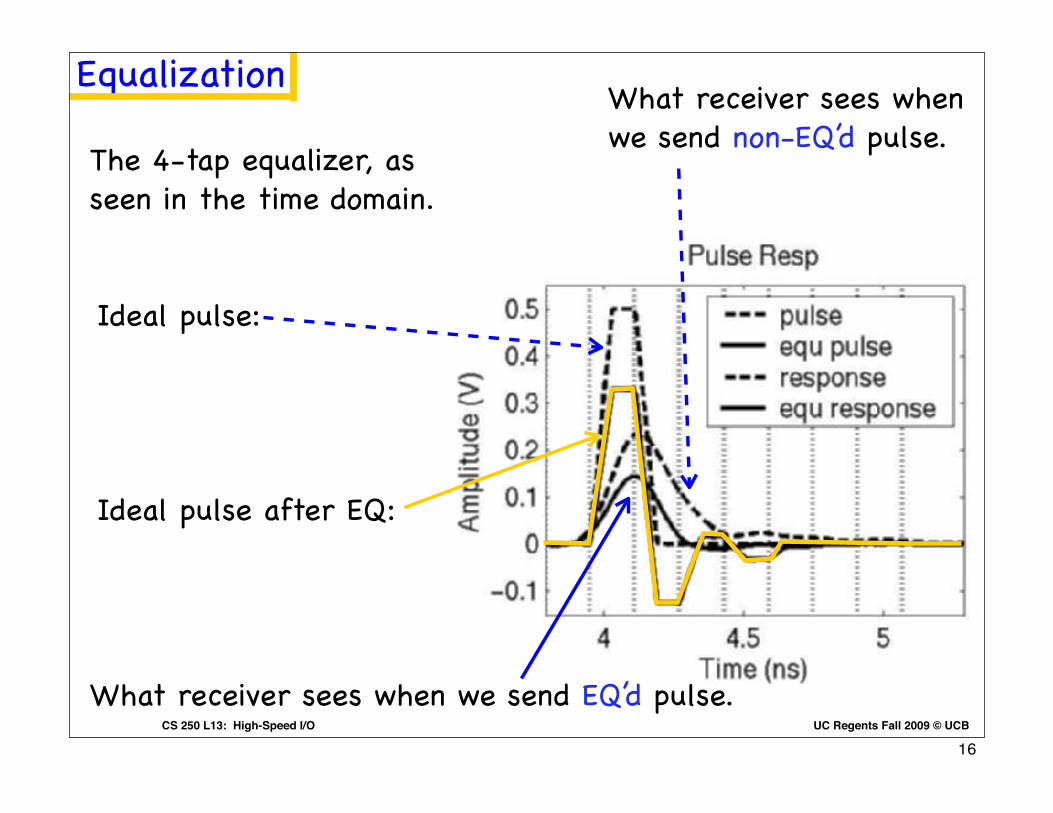
UC Regents Fall 2009 © UCBCS 250 L13: High-Speed I/O
Equalization
The 4-tap equalizer, as seen in the time domain.
Time
Jitter
PLL
MDLL
Tref
Figure 6: Jitter Response of a PLL and a MDLL.
PhaseFilter
FreqFilter
FreqEstimate
FreqGenerate
TimingVernier
AlexanderPD
RxInput
Freq-Tracking Loop
Clock MultiplierRef Clk
up/dn
early/late
First-Order Loop
Figure 7: A digital clock recovery architecture.
grammable (e.g., to maximize jitter filtering or minimizelock time). Furthermore, the digital control to the timingvernier can be easily bypassed to allow flexible position-ing of the sampling clocks for testing purposes.
2.5. Equalization
Skin effect, dielectric absorption and discontinu-ities cause a channel to exhibit frequency-dependent loss(FDL). A pulse representing a bit not only gets atten-uated by the channel but is spread out in time, caus-ing ISI. Figure 8 shows the frequency response and the6.25 Gb/s pulse response of a backplane channel. A sig-nificant amount of ISI is present at the adjacent sam-ple points in the pulse response (the vertical grid lines arespaced at the sample points, 160 ps apart).
A filter, or equalizer, with an inverse channel responsecan be used to counteract FDL. A commonly used filter is adiscrete-time symbol-spaced FIR filter. Oftentimes it is im-plemented at the transmitter (transmitter pre-emphasis) withdirect current summing of different taps at the output [3][11]. Figure 8 shows the effect of a 4-tap filter (1 main tapand 3 post-cursor taps) in the frequency domain and timedomain on the same backplane channel. Since a portion ofthe available transmitter current is assigned to the equaliza-tion taps, in effect transmitter pre-emphasis attenuates thelow-frequency component to achieve a flat spectrum over-all. With pre-emphasis, the amount of ISI is significantly
Figure 8: Response of a backplane channel.
in+ in-
bias
out
Figure 9: Active RC-based receive equalization.
reduced. As shown in Figure 8, it opens up a completelyclosed eye (PRBS 23 pattern).
Sometimes it is beneficial to place the equalizer at the re-ceiver. Although a discrete-time FIR approach can be used,it is significantly more complicated than transmitter pre-emphasis since high-speed sampling, multiplication, andaddition of analog values are required. An alternative isan active high-pass filter, shown in Figure 9 [6]. The gainof this circuit goes up with frequency as the capacitor de-creases the amount of source degeneration. The equaliza-tion gain can be adjusted through the variable resistors.
3. Future Challenges
As gate lengths are scaled by α (at a rate of about 20%per year), gate delay also scales as α and transistor ωT
scales as 1/α. Signaling bandwidth can also scale as 1/α ifthe timing uncertainties, dominated by clock jitter and chan-nel interference can be made to scale at the same rate. Thissection investigates the scalability of clock jitter and dis-
!"#$%%&'()*+#,+-.%+/0*-+1(-%"(2-'#(23+4#(,%"%($%+#(+4#567-%"+8%*')(+91448:;<=+0;><?>@;@A;<+B+0CD;;+E+/;;<+1FFF+
Ideal pulse:
Ideal pulse after EQ:
What receiver sees when we send non-EQ’d pulse.
What receiver sees when we send EQ’d pulse.16

UC Regents Fall 2009 © UCBCS 250 L13: High-Speed I/O
Eye Diagrams
17

UC Regents Fall 2009 © UCBCS 250 L13: High-Speed I/O
Eye diagrams A way to visualize bits on a wire.
IEEE JOURNAL OF SOLID-STATE CIRCUITS, VOL. 36, NO. 4, APRIL 2001 709
Fig. 5. Schematic diagram of the improved LVDS receiver supporting the fullinput range of the LVDS standard.
Fig. 6. Chip photograph of the transmitter chipset: SR is the serializer cir-cuitry, CCO is the controlled oscillator, and B.G.REF. is the biasing circuitry.
, in order to keep the voltage gain almost insensitive
to the input common-mode voltage. Since the input devices are
designed with a large aspect ratio, in order to achieve a sufficient
voltage gain, the impedance level at the drain of those devices is
critical in order to obtain the required bandwidth. The problem is
easily overcome by means of the cascode configuration, which
ensures a low small-signal resistance at nodes and . The
value of the load resistors, , is optimized so as to achieve
at the same time the required voltage gain, bandwidth, and the
correct common-mode voltage for the second differential gain
stage. Since the aspect ratio of the nMOS input devices of the
Fig. 7. Measured CK and DATA waveforms with a 11 010 010 pattern trans-mitted at 1 Gb/s.
Fig. 8. Measured eye pattern at 1 Gb/s. The probe bandwidth is limited to1 GHz.
second stage is about one order of magnitude lower than the as-
pect ratio of , the impact of on the overall
bandwidth is quite limited. Biasing voltages and are set
to 1.05 and 2.1 V, respectively (typical values). Input transistors,
and , experience a minimum source-to-drain voltage of
about 250 mV with 0.1-V common-mode voltage at the input.
The second stage is a nMOS version of the typical LVDS
receiver, Fig. 4, where the choice of pMOS input devices was
mainly determined by the input common-mode range to be sup-
ported. In the proposed receiver, the use of nMOS input devices
for the second stage has the advantage that the same voltage gain
can be achieved with lower aspect ratios, thus providing a larger
bandwidth. The implemented pad cell exhibits an area of about
0.08 mm and a current consumption of 10 mA at 1 Gb/s.
III. EXPERIMENTAL RESULTS
The two circuits were implemented in a couple of test chips in
a 0.35- m CMOS technology [16], Fig. 6. The transmitter is a
serializer transmitting a 8-bit data burst with a 90 shifted clock
reference over two pairs of 3-cm-long, 0.6-mm-large 50-
-strip lines (FR4 thickness is 360 m). The transmission speed
is set by means of an internal current-controlled oscillator. The
receiver is a serial-to-parallel converter which allows to verify
the performance of the proposed LVDS receiver. Measurements
were performed up to 1.2 Gb/s with random data patterns. Fig. 7
shows themeasuredCK andDATAwaveformswith a 11 010 010
pattern transmitted at 1 Gb/s, while the eye pattern at 1 Gb/s is
shown in Fig. 8. A 1-GHz differential probe was used for the
measurements.
Oscilloscope trace of receive-end of wire.
IEEE JOURNAL OF SOLID-STATE CIRCUITS, VOL. 36, NO. 4, APRIL 2001 709
Fig. 5. Schematic diagram of the improved LVDS receiver supporting the fullinput range of the LVDS standard.
Fig. 6. Chip photograph of the transmitter chipset: SR is the serializer cir-cuitry, CCO is the controlled oscillator, and B.G.REF. is the biasing circuitry.
, in order to keep the voltage gain almost insensitive
to the input common-mode voltage. Since the input devices are
designed with a large aspect ratio, in order to achieve a sufficient
voltage gain, the impedance level at the drain of those devices is
critical in order to obtain the required bandwidth. The problem is
easily overcome by means of the cascode configuration, which
ensures a low small-signal resistance at nodes and . The
value of the load resistors, , is optimized so as to achieve
at the same time the required voltage gain, bandwidth, and the
correct common-mode voltage for the second differential gain
stage. Since the aspect ratio of the nMOS input devices of the
Fig. 7. Measured CK and DATA waveforms with a 11 010 010 pattern trans-mitted at 1 Gb/s.
Fig. 8. Measured eye pattern at 1 Gb/s. The probe bandwidth is limited to1 GHz.
second stage is about one order of magnitude lower than the as-
pect ratio of , the impact of on the overall
bandwidth is quite limited. Biasing voltages and are set
to 1.05 and 2.1 V, respectively (typical values). Input transistors,
and , experience a minimum source-to-drain voltage of
about 250 mV with 0.1-V common-mode voltage at the input.
The second stage is a nMOS version of the typical LVDS
receiver, Fig. 4, where the choice of pMOS input devices was
mainly determined by the input common-mode range to be sup-
ported. In the proposed receiver, the use of nMOS input devices
for the second stage has the advantage that the same voltage gain
can be achieved with lower aspect ratios, thus providing a larger
bandwidth. The implemented pad cell exhibits an area of about
0.08 mm and a current consumption of 10 mA at 1 Gb/s.
III. EXPERIMENTAL RESULTS
The two circuits were implemented in a couple of test chips in
a 0.35- m CMOS technology [16], Fig. 6. The transmitter is a
serializer transmitting a 8-bit data burst with a 90 shifted clock
reference over two pairs of 3-cm-long, 0.6-mm-large 50-
-strip lines (FR4 thickness is 360 m). The transmission speed
is set by means of an internal current-controlled oscillator. The
receiver is a serial-to-parallel converter which allows to verify
the performance of the proposed LVDS receiver. Measurements
were performed up to 1.2 Gb/s with random data patterns. Fig. 7
shows themeasuredCK andDATAwaveformswith a 11 010 010
pattern transmitted at 1 Gb/s, while the eye pattern at 1 Gb/s is
shown in Fig. 8. A 1-GHz differential probe was used for the
measurements.
Fold the trace at the clock period. If the received signal is clean, an open eye is seen.
18
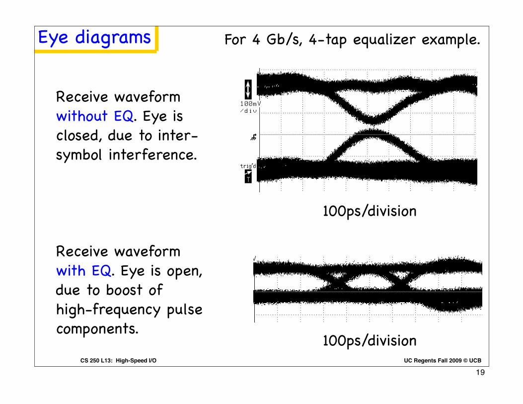
UC Regents Fall 2009 © UCBCS 250 L13: High-Speed I/O
Eye diagrams For 4 Gb/s, 4-tap equalizer example.
Receive waveform with EQ. Eye is open, due to boost of high-frequency pulse components.
on to the line by a clock generator to generate the output
signal.
Output waveforms from the transmitter are shown in
Figure 6. The figure shows an isolated 250ps one pulse in
a field of zeros being transmitted across 1m of 30AWG
twisted-pair cable. The waveform on the left is without
equalization. With 10dB of attenuation there is no eye
opening and the one is undetectable. With equalization, as
shown on the right, a clean 250ps eye opening is visible.
Figure 6: Measured waveforms from 4Gb/s test chip with
equalization off (left) and on (right).
A demultiplexing receiver, also operating at 400MHz is
used to receive the signal as shown in Figure 7. The line is
received by a bank of 20 clocked sense amplifiers. Each
amplifier is allowed 1.25ns, about 10 time constants, to set-
tle giving very good sensitivity. The amplifiers sample the
10 data bits as well as the 10 potential edges between the
bits. The edge samples are used to control the 20-phase
clock. By centering the odd samples on the edges, the even
samples remain centered on the eye openings.
Figure 7: Block diagram of 4Gb/s receiver
4.2 Input Multiplexed Architecture
While our initial test chip was successful in demonstrat-
ing equalized signaling at 4Gb/s rates it had two significant
shortcomings: (a) the transmitter was very large, measur-
ing 1mm x 0.5mm, and (b) the source-coupled delay lines
used for transmitter and receiver timing consumed consid-
erable power. While our first design is adequate for a chip
with up to a few tens of transceivers, a smaller, lower-
power transceiver is required to enable hundreds of 4Gb/s
transceivers to be placed on a chip.
After experimenting with several alternatives, we
arrived at the input-multiplexed transmitter architecture
using analog equalization to achieve our size and power
goals. A block diagram of this transmitter is shown in Fig-
ure 8. Equalization is performed by a two-tap analog filter
that is realized by having the main transmitter and an
equalizing duplicate transmitter sum their output currents
on the line. The equalizing duplicate operates one bit
delayed and with programmable weight. Longer analog
FIR filters can be constructed by building additional dupli-
cates each delayed one bit from the previous duplicate.
Figure 8: Input-multiplexed transmitter architecture with
analog equalization
The input-multiplexed transmitter of Figure 8 is consid-
erably smaller than the output-multiplexed transmitter of
Figure 7. While layout of the new transmitter is not yet
complete, we estimate that it will fit in an area of 0.1mm !
0.1mm, about 2% of the area of the old transmitter. This
reduction in area is due to three factors. First, there is only
a single copy of the transmitter circuitry as opposed to ten
copies in the previous design. Second, using an analog
equalizing filter eliminates the costly look-up table RAMs.
Finally, operating the transmitter circuitry at 1GHz rather
than 400MHz allows us to operate with 4:1 multiplexing
instead of 10:1 multiplexing reducing the required size of
the multiplexer and clock delay line.
The new design is also considerably more power-effi-
cient than the previous design. While we have not com-
pleted our power studies at this time, we anticipate
considerable gains in three areas. First, by moving the
multiplexer to the input the clock load, and hence the clock
power, is reduced by an order of magnitude. Second, this
design uses a clock circuit based on regulated CMOS
delay stages, as opposed to the source-coupled delay stages
in the previous design, that dissipates about a third the
power for a given clock load. Finally, all of the power pre-
viously dissipated in the digital filters has been eliminated.
5. Conclusion
Incident-wave electrical signaling systems currently
operate at data rates up to 4Gb/s. We expect these signal-
ing rates to improve on a Moore’s law curve over time
because all of the electronic factors limiting performance
scale with improving semiconductor technology.
At a given signaling rate, signaling distance, without
repeaters, is limited by the frequency-dependent attenua-
tion of the transmission medium. This limitation can be
Demultiplexing
ReceiverIn+In-
20-PhaseClock Generator
Clock
(400MHz)
20
10
10 ClockControl
E0-9
Retiming D0-9 10
Mu
x
ClampPreamp
4
Driver
D0-3
1GHz
4! Clock1GHz
EqualizingDuplicate
100ps/division
Receive waveform without EQ. Eye is closed, due to inter-symbol interference.
on to the line by a clock generator to generate the output
signal.
Output waveforms from the transmitter are shown in
Figure 6. The figure shows an isolated 250ps one pulse in
a field of zeros being transmitted across 1m of 30AWG
twisted-pair cable. The waveform on the left is without
equalization. With 10dB of attenuation there is no eye
opening and the one is undetectable. With equalization, as
shown on the right, a clean 250ps eye opening is visible.
Figure 6: Measured waveforms from 4Gb/s test chip with
equalization off (left) and on (right).
A demultiplexing receiver, also operating at 400MHz is
used to receive the signal as shown in Figure 7. The line is
received by a bank of 20 clocked sense amplifiers. Each
amplifier is allowed 1.25ns, about 10 time constants, to set-
tle giving very good sensitivity. The amplifiers sample the
10 data bits as well as the 10 potential edges between the
bits. The edge samples are used to control the 20-phase
clock. By centering the odd samples on the edges, the even
samples remain centered on the eye openings.
Figure 7: Block diagram of 4Gb/s receiver
4.2 Input Multiplexed Architecture
While our initial test chip was successful in demonstrat-
ing equalized signaling at 4Gb/s rates it had two significant
shortcomings: (a) the transmitter was very large, measur-
ing 1mm x 0.5mm, and (b) the source-coupled delay lines
used for transmitter and receiver timing consumed consid-
erable power. While our first design is adequate for a chip
with up to a few tens of transceivers, a smaller, lower-
power transceiver is required to enable hundreds of 4Gb/s
transceivers to be placed on a chip.
After experimenting with several alternatives, we
arrived at the input-multiplexed transmitter architecture
using analog equalization to achieve our size and power
goals. A block diagram of this transmitter is shown in Fig-
ure 8. Equalization is performed by a two-tap analog filter
that is realized by having the main transmitter and an
equalizing duplicate transmitter sum their output currents
on the line. The equalizing duplicate operates one bit
delayed and with programmable weight. Longer analog
FIR filters can be constructed by building additional dupli-
cates each delayed one bit from the previous duplicate.
Figure 8: Input-multiplexed transmitter architecture with
analog equalization
The input-multiplexed transmitter of Figure 8 is consid-
erably smaller than the output-multiplexed transmitter of
Figure 7. While layout of the new transmitter is not yet
complete, we estimate that it will fit in an area of 0.1mm !
0.1mm, about 2% of the area of the old transmitter. This
reduction in area is due to three factors. First, there is only
a single copy of the transmitter circuitry as opposed to ten
copies in the previous design. Second, using an analog
equalizing filter eliminates the costly look-up table RAMs.
Finally, operating the transmitter circuitry at 1GHz rather
than 400MHz allows us to operate with 4:1 multiplexing
instead of 10:1 multiplexing reducing the required size of
the multiplexer and clock delay line.
The new design is also considerably more power-effi-
cient than the previous design. While we have not com-
pleted our power studies at this time, we anticipate
considerable gains in three areas. First, by moving the
multiplexer to the input the clock load, and hence the clock
power, is reduced by an order of magnitude. Second, this
design uses a clock circuit based on regulated CMOS
delay stages, as opposed to the source-coupled delay stages
in the previous design, that dissipates about a third the
power for a given clock load. Finally, all of the power pre-
viously dissipated in the digital filters has been eliminated.
5. Conclusion
Incident-wave electrical signaling systems currently
operate at data rates up to 4Gb/s. We expect these signal-
ing rates to improve on a Moore’s law curve over time
because all of the electronic factors limiting performance
scale with improving semiconductor technology.
At a given signaling rate, signaling distance, without
repeaters, is limited by the frequency-dependent attenua-
tion of the transmission medium. This limitation can be
Demultiplexing
ReceiverIn+In-
20-PhaseClock Generator
Clock
(400MHz)
20
10
10 ClockControl
E0-9
Retiming D0-9 10
Mu
x
ClampPreamp
4
Driver
D0-3
1GHz
4! Clock1GHz
EqualizingDuplicate
100ps/division
19

UC Regents Fall 2009 © UCBCS 250 L13: High-Speed I/O
Eye diagrams What limits bandwidth?
For a typical 0.35µm (drawn gate length) CMOS pro-
cess, !n = 10ps, and this time constant scales linearly with
gate length.
Figure 3: Abstract eye diagram showing limitations on sig-
naling rate.
The transition time of the signal, tr, is determined by the
time required to slew the current source from one extreme
to the other. Using a current source switched by logic gates
it is easy to generate a slew time of 10!n, 100ps in an
0.35µm process. The RC time constant of the terminated
line (25") and the capacitance of the driver (about 1pF) is
smaller than the driver slew time.
The aperture time of the receive amplifier, ta, can be
made as small as 2!n by using a gate-isolated sense ampli-
fier [DP98]. Using a pass-gate to sample the arriving sig-
nal gives an aperture time of about 10!n.
The peak-to-peak jitter, 2tu, is caused by jitter in the
sampling clock, jitter in the receive clock, and delay varia-
tions in the signal path. All three sources of jitter are pri-
marily due to power-supply modulation of delay and
crosstalk-induced delay variation. Both of these factors
scale with delay and hence with process gate length. Using
circuits with good power supply rejection and layout tech-
niques to avoid crosstalk, peak-to-peak jitter of less than
5!n can be achieved.
As gate lengths shrink, variation in device parameters,
such as VT is expected to increase. This variation will lead
to a fixed variation in, for example, the delay elements
used to build timing circuits. Left uncompensated, this
effect would give fixed-pattern jitter term that does not
scale linearly with process technology. Fortunately, it is
possible to measure these variations and compensate for
them.
With careful design, an incident-wave signaling system
can achieve a bit cell width of 15-30!n (150-300ps in
0.35µm technology). Most importantly, because there is
no need to ring up the signal line, this signaling rate scales
linearly with the basic time constant of the technology, !n,
independent of the wire length. As gate lengths continue to
shrink according to the SIA roadmap [SIA97] the speed of
signaling systems can improve at the same rate.
3.2 Wire Limits on Signaling Rate
While the speed of the transmitter and receiver improve
as the gate length of semiconductor technology shrinks, the
bandwith of the wire used to connect the transmitter to the
receiver remains constant. For interconnects that traverse
any appreciable distance, the bandwidth of this wire is rap-
idly becoming the limiting factor. We can express this lim-
itation as a bandwidth-distance squared product with units
of bits#m2/s [MO97].
Frequency-dependent attenuation due to the skin-effect
resistance of the wire is the major factor limiting wire
bandwidth. Impedance discontinuities are not a limiting
factor. In a well designed system, the transmission path
from transmitter to receiver has a constant impedance with
no appreciable discontinuities to attenuate the signal and
cause inter-symbol interference. With some insulating
materials, dielectric absorption also causes frequency-
dependent attenuation; however this effect can be miti-
gated by using a low-loss dielectric.
The skin-effect attenuation in dB at frequency f of a
wire with length d is given by
(2)
where A1 is the attenuation of a 1m wire at frequency f1.
For example, the attenuation of a 100", 24AWG twisted
pair is 0.45dB/m at 1GHz (A1 = 0.45dB/m, f1 = 1GHz). At
10GHz a 1m wire has an attenuation of 1.4dB/m and a 10m
wire has an attenuation of 14dB. Attenuation is also pro-
portional to the inverse of the wire radius, so one can get
lower attenuation by using fatter wires. However, for the
remainder of this discussion we will use the 24AWG cable
for our illustrative example.
Because this attenuation is frequency dependent it
causes inter-symbol interference in addition to reducing
signal energy. At an attenuation of 6dB, the unattenuated
low frequency components of the signal completely swamp
the high frequency components. Because of this effect,
transmission without equalization is usually limited to an
attenuation of 2dB or less. If our tolerable attenuation in
dB is AT and our bandwidth in bits/s is B = 2f, then we can
rewrite Equation (2) as
(3)
For an unequalized 24AWG pair, the Bd2 product is lim-
ited to 4 # 1010 bits#m2/s. Without equalization this cable
can carry 40Gb/s over 1m or 400Mb/s over 10m.
Equalizing the signal, by pre-emphasizing the high-fre-
quency components of the signal before transmission,
eliminates the inter-symbol interference caused by the fre-
quency-dependent nature of the attenuation. To date we
have demonstrated signaling systems that can equalize up
to 10dB of frequency-dependent attenuation. From Equa-
tion (3) the Bd2 product for a 24-gauge cable with this lim-
ited equalization is 1012 bits#m2/s, 1Tb/s over 1m or 10Gb/
s over 10m. Better equalization can improve this capacity
further.
2tu
2tu
ta tr
tr ta tm
A d f,( ) A1df
f1
----$ %& '
1
2---
=
Bd2
2f1
AT
A1
------$ %& '
2
=
Rise time. Depends on drive current of output transistor.
Aperture time. How long it takes sense amp to make +/- decision.
Uncertainty time. All sources of temporal uncertainty (jitter, etc).
All should improve with process, but all have fundamental limits (thermal noise, non-perfect line equalization, etc).
20

UC Regents Fall 2009 © UCBCS 250 L13: High-Speed I/O
Clock Recovery
21
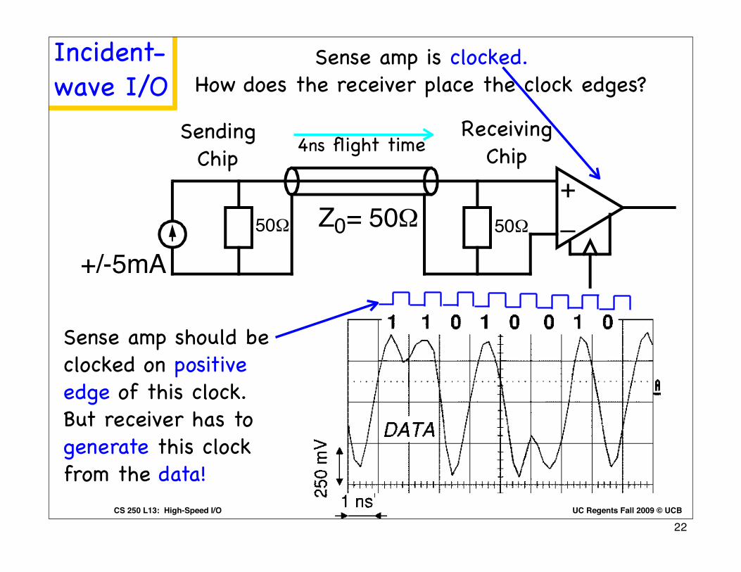
UC Regents Fall 2009 © UCBCS 250 L13: High-Speed I/O
modern microprocessors operate their external buses at
small fraction of their internal clock rate.
Figure 1: A traditional CMOS signaling system.
Figure 1 shows a traditional CMOS signaling system.
CMOS inverters are used as both driver and receiver. The
transmission medium, typically a cable or PC-board trace
has a characteristic impedance of about 50!. The driver
typically has an output impedance of 400! and the line is
unterminated at the receiver. The two power supplies
(VDD = 3.3V and GND = 0V) are used to represent logic 1
and 0 respectively.
The traditional CMOS system is slow because the high
impedance driver is unable to switch the line on the inci-
dent wave. Instead, the driver must ring up the line as the
signal propagates over several round-trips of the line as
shown in Figure 2. The figure shows the voltage as a frac-
tion of VDD at the far end of the line as a function of time.
The incident wave only switches the line to 10% of VDD.
This is doubled by the first reflection at 10ns. Seven tra-
versals of the 4ns line are required to ring the line up to
50% of VDD, and over 15 traversals are needed for the line
to converge to within 10% of its final value.
Figure 2: An 8mA CMOS Driver rings up a 4ns line termi-
nated into 1K!.
The traditional CMOS system is power hungry, dissipat-
ing 1nJ or more to transmit each bit because it requires
large signal swings to overcome poor noise isolation. The
system uses noisy power supplies as transmit and receive
voltage references. It also uses a CMOS inverter which
has both a large offset voltage across process corners (typi-
cally 300mV) and poor sensitivity (about 500mV) as a
receiver. To overcome these noise sources, a large signal
swing, typically the full power supply, is required.
2.2 Low-Swing, Incident-Wave Signaling
A signaling system that overcomes the limitations of
traditional CMOS signaling is shown in Figure 2. A cur-
rent-source transmitter drives the line. A typical drive is
±5mA which gives a 250mV signal swing. The line is ter-
minated at both ends into its characteristic impedance. The
receiver termination absorbs the incident wave preventing
any reflections. The source termination makes the system
more tolerant of crosstalk and impedance discontinuities
by absorbing any ‘stray’ waves that arrive back at the
source. A high-gain clocked regenerative receive amplifier
gives low offset (typically 10mV) and good sensitivity
(10mV or better depending on settling time).
Figure 2: A low-swing, incident-wave signaling system.
By operating using only the incident wave, the system
of Figure 2 can operate at a data rate independent of the
length of the line. A new bit can be driven onto the source
end of the line before the previous bit arrives at the
receiver. As discussed below, this results in a data rate
that, to first approximation, scales linearly with device
speed.
This system operates reliably using a very small voltage
swing (250mV) because it isolates the signal from many
noise sources. Transmit and receive references are isolated
from the noisy power supplies and a clocked receive ampli-
fier greatly improves offset and sensitivity.
3. Limitations on Signaling Rate
The data rate of a signaling system is limited by both the
electronics used to generate and receive the signal and the
medium over which the signal propagates.
3.1 Electronic Limits on Signaling Rate
As illustrated in Figure 3, electronics limits signaling
rate due to rise-time, aperture time, and timing uncertainty
[DP98b]. The time for a bit cell, tbit, must be made long
enough for the signal to slew from one logic level to
another, tr, for the receiver to sample this signal while sta-
ble, ta, and to tolerate jitter between the signal and the sam-
pling clock, 2tu.
All three of these factors are related to the basic time
constant of the semiconductor technology,"n, the time for a
minimum-sized nFET to discharge the gate of an equal-
sized nFET [DP98b]. This time constant is given approxi-
mately by
. (1)
RO= 400! Z0= 50! A=6
0
0.2
0.4
0.6
0.8
0 20 40 60 80
Time (nsec)
Z0= 50!
RO= 50!
+
–
RT= 50!
+/-5mA
"n
VDDCg
IDSS
-----------------=
Incident-wave I/O
modern microprocessors operate their external buses at
small fraction of their internal clock rate.
Figure 1: A traditional CMOS signaling system.
Figure 1 shows a traditional CMOS signaling system.
CMOS inverters are used as both driver and receiver. The
transmission medium, typically a cable or PC-board trace
has a characteristic impedance of about 50!. The driver
typically has an output impedance of 400! and the line is
unterminated at the receiver. The two power supplies
(VDD = 3.3V and GND = 0V) are used to represent logic 1
and 0 respectively.
The traditional CMOS system is slow because the high
impedance driver is unable to switch the line on the inci-
dent wave. Instead, the driver must ring up the line as the
signal propagates over several round-trips of the line as
shown in Figure 2. The figure shows the voltage as a frac-
tion of VDD at the far end of the line as a function of time.
The incident wave only switches the line to 10% of VDD.
This is doubled by the first reflection at 10ns. Seven tra-
versals of the 4ns line are required to ring the line up to
50% of VDD, and over 15 traversals are needed for the line
to converge to within 10% of its final value.
Figure 2: An 8mA CMOS Driver rings up a 4ns line termi-
nated into 1K!.
The traditional CMOS system is power hungry, dissipat-
ing 1nJ or more to transmit each bit because it requires
large signal swings to overcome poor noise isolation. The
system uses noisy power supplies as transmit and receive
voltage references. It also uses a CMOS inverter which
has both a large offset voltage across process corners (typi-
cally 300mV) and poor sensitivity (about 500mV) as a
receiver. To overcome these noise sources, a large signal
swing, typically the full power supply, is required.
2.2 Low-Swing, Incident-Wave Signaling
A signaling system that overcomes the limitations of
traditional CMOS signaling is shown in Figure 2. A cur-
rent-source transmitter drives the line. A typical drive is
±5mA which gives a 250mV signal swing. The line is ter-
minated at both ends into its characteristic impedance. The
receiver termination absorbs the incident wave preventing
any reflections. The source termination makes the system
more tolerant of crosstalk and impedance discontinuities
by absorbing any ‘stray’ waves that arrive back at the
source. A high-gain clocked regenerative receive amplifier
gives low offset (typically 10mV) and good sensitivity
(10mV or better depending on settling time).
Figure 2: A low-swing, incident-wave signaling system.
By operating using only the incident wave, the system
of Figure 2 can operate at a data rate independent of the
length of the line. A new bit can be driven onto the source
end of the line before the previous bit arrives at the
receiver. As discussed below, this results in a data rate
that, to first approximation, scales linearly with device
speed.
This system operates reliably using a very small voltage
swing (250mV) because it isolates the signal from many
noise sources. Transmit and receive references are isolated
from the noisy power supplies and a clocked receive ampli-
fier greatly improves offset and sensitivity.
3. Limitations on Signaling Rate
The data rate of a signaling system is limited by both the
electronics used to generate and receive the signal and the
medium over which the signal propagates.
3.1 Electronic Limits on Signaling Rate
As illustrated in Figure 3, electronics limits signaling
rate due to rise-time, aperture time, and timing uncertainty
[DP98b]. The time for a bit cell, tbit, must be made long
enough for the signal to slew from one logic level to
another, tr, for the receiver to sample this signal while sta-
ble, ta, and to tolerate jitter between the signal and the sam-
pling clock, 2tu.
All three of these factors are related to the basic time
constant of the semiconductor technology,"n, the time for a
minimum-sized nFET to discharge the gate of an equal-
sized nFET [DP98b]. This time constant is given approxi-
mately by
. (1)
RO= 400! Z0= 50! A=6
0
0.2
0.4
0.6
0.8
0 20 40 60 80
Time (nsec)
Z0= 50!
RO= 50!
+
–
RT= 50!
+/-5mA
"n
VDDCg
IDSS
-----------------=
modern microprocessors operate their external buses at
small fraction of their internal clock rate.
Figure 1: A traditional CMOS signaling system.
Figure 1 shows a traditional CMOS signaling system.
CMOS inverters are used as both driver and receiver. The
transmission medium, typically a cable or PC-board trace
has a characteristic impedance of about 50!. The driver
typically has an output impedance of 400! and the line is
unterminated at the receiver. The two power supplies
(VDD = 3.3V and GND = 0V) are used to represent logic 1
and 0 respectively.
The traditional CMOS system is slow because the high
impedance driver is unable to switch the line on the inci-
dent wave. Instead, the driver must ring up the line as the
signal propagates over several round-trips of the line as
shown in Figure 2. The figure shows the voltage as a frac-
tion of VDD at the far end of the line as a function of time.
The incident wave only switches the line to 10% of VDD.
This is doubled by the first reflection at 10ns. Seven tra-
versals of the 4ns line are required to ring the line up to
50% of VDD, and over 15 traversals are needed for the line
to converge to within 10% of its final value.
Figure 2: An 8mA CMOS Driver rings up a 4ns line termi-
nated into 1K!.
The traditional CMOS system is power hungry, dissipat-
ing 1nJ or more to transmit each bit because it requires
large signal swings to overcome poor noise isolation. The
system uses noisy power supplies as transmit and receive
voltage references. It also uses a CMOS inverter which
has both a large offset voltage across process corners (typi-
cally 300mV) and poor sensitivity (about 500mV) as a
receiver. To overcome these noise sources, a large signal
swing, typically the full power supply, is required.
2.2 Low-Swing, Incident-Wave Signaling
A signaling system that overcomes the limitations of
traditional CMOS signaling is shown in Figure 2. A cur-
rent-source transmitter drives the line. A typical drive is
±5mA which gives a 250mV signal swing. The line is ter-
minated at both ends into its characteristic impedance. The
receiver termination absorbs the incident wave preventing
any reflections. The source termination makes the system
more tolerant of crosstalk and impedance discontinuities
by absorbing any ‘stray’ waves that arrive back at the
source. A high-gain clocked regenerative receive amplifier
gives low offset (typically 10mV) and good sensitivity
(10mV or better depending on settling time).
Figure 2: A low-swing, incident-wave signaling system.
By operating using only the incident wave, the system
of Figure 2 can operate at a data rate independent of the
length of the line. A new bit can be driven onto the source
end of the line before the previous bit arrives at the
receiver. As discussed below, this results in a data rate
that, to first approximation, scales linearly with device
speed.
This system operates reliably using a very small voltage
swing (250mV) because it isolates the signal from many
noise sources. Transmit and receive references are isolated
from the noisy power supplies and a clocked receive ampli-
fier greatly improves offset and sensitivity.
3. Limitations on Signaling Rate
The data rate of a signaling system is limited by both the
electronics used to generate and receive the signal and the
medium over which the signal propagates.
3.1 Electronic Limits on Signaling Rate
As illustrated in Figure 3, electronics limits signaling
rate due to rise-time, aperture time, and timing uncertainty
[DP98b]. The time for a bit cell, tbit, must be made long
enough for the signal to slew from one logic level to
another, tr, for the receiver to sample this signal while sta-
ble, ta, and to tolerate jitter between the signal and the sam-
pling clock, 2tu.
All three of these factors are related to the basic time
constant of the semiconductor technology,"n, the time for a
minimum-sized nFET to discharge the gate of an equal-
sized nFET [DP98b]. This time constant is given approxi-
mately by
. (1)
RO= 400! Z0= 50! A=6
0
0.2
0.4
0.6
0.8
0 20 40 60 80
Time (nsec)
Z0= 50!
RO= 50!
+
–
RT= 50!
+/-5mA
"n
VDDCg
IDSS
-----------------=
4ns flight timeSending Chip
Receiving Chip
Sense amp is clocked. How does the receiver place the clock edges?
IEEE JOURNAL OF SOLID-STATE CIRCUITS, VOL. 36, NO. 4, APRIL 2001 709
Fig. 5. Schematic diagram of the improved LVDS receiver supporting the fullinput range of the LVDS standard.
Fig. 6. Chip photograph of the transmitter chipset: SR is the serializer cir-cuitry, CCO is the controlled oscillator, and B.G.REF. is the biasing circuitry.
, in order to keep the voltage gain almost insensitive
to the input common-mode voltage. Since the input devices are
designed with a large aspect ratio, in order to achieve a sufficient
voltage gain, the impedance level at the drain of those devices is
critical in order to obtain the required bandwidth. The problem is
easily overcome by means of the cascode configuration, which
ensures a low small-signal resistance at nodes and . The
value of the load resistors, , is optimized so as to achieve
at the same time the required voltage gain, bandwidth, and the
correct common-mode voltage for the second differential gain
stage. Since the aspect ratio of the nMOS input devices of the
Fig. 7. Measured CK and DATA waveforms with a 11 010 010 pattern trans-mitted at 1 Gb/s.
Fig. 8. Measured eye pattern at 1 Gb/s. The probe bandwidth is limited to1 GHz.
second stage is about one order of magnitude lower than the as-
pect ratio of , the impact of on the overall
bandwidth is quite limited. Biasing voltages and are set
to 1.05 and 2.1 V, respectively (typical values). Input transistors,
and , experience a minimum source-to-drain voltage of
about 250 mV with 0.1-V common-mode voltage at the input.
The second stage is a nMOS version of the typical LVDS
receiver, Fig. 4, where the choice of pMOS input devices was
mainly determined by the input common-mode range to be sup-
ported. In the proposed receiver, the use of nMOS input devices
for the second stage has the advantage that the same voltage gain
can be achieved with lower aspect ratios, thus providing a larger
bandwidth. The implemented pad cell exhibits an area of about
0.08 mm and a current consumption of 10 mA at 1 Gb/s.
III. EXPERIMENTAL RESULTS
The two circuits were implemented in a couple of test chips in
a 0.35- m CMOS technology [16], Fig. 6. The transmitter is a
serializer transmitting a 8-bit data burst with a 90 shifted clock
reference over two pairs of 3-cm-long, 0.6-mm-large 50-
-strip lines (FR4 thickness is 360 m). The transmission speed
is set by means of an internal current-controlled oscillator. The
receiver is a serial-to-parallel converter which allows to verify
the performance of the proposed LVDS receiver. Measurements
were performed up to 1.2 Gb/s with random data patterns. Fig. 7
shows themeasuredCK andDATAwaveformswith a 11 010 010
pattern transmitted at 1 Gb/s, while the eye pattern at 1 Gb/s is
shown in Fig. 8. A 1-GHz differential probe was used for the
measurements.
Sense amp should be clocked on positive edge of this clock. But receiver has to generate this clock from the data!
22

UC Regents Fall 2009 © UCBCS 250 L13: High-Speed I/O
Alexanderdetector
9
The expected phase change in the loop after one update time is
The discrete time equation for the average evolution of loop phaseunder the condition of a small input phase error can then beexpressed as
This equation has the same form as a discrete time approximationto the capacitor voltage in an RC lowpass filter. By analogy, whentime is expressed in units of loop update times, any transient phaseerror in the bang-bang loop can then be said to decay to zero with
a time constant of .
This “lowpass” loop characteristic is being driven by randomenergy from the early/late phase detector output. A related prob-lem is the computation of the baseline wander voltage generatedby passing a random NRZ data stream through a coupling capaci-tor. It can be shown that the sigma on the capacitor voltage is
given by . Extending this analogy to
the loop, we can consider the output of the phase detector as a50% duty-cycle random NRZ data stream. Given that the output
from each “bit” must cause a loop phase change of , we can
compute that the effective to satisfy our loop difference
equation must be . We can then compute the loop jitter by
using the analogous baseline wander expression with the effective
loop and . The result is
which is consistent with empirical analysis of simulation results.
One further insight into this behavior is offered. The second-order loop drives the phase detector output to a steady-state 50%duty-cycle. In this condition, the loop phase splits the input jitterdistribution into equal early and late halves. This means that thebang-bang loop phase is servoed to the median of the input jitterdistribution rather than to the mean as would be the case with alinear loop. Because of this, the bang-bang loop makes a constantmodest correction in response to large jitter outliers, rather thanthe proportionally large overcompensation of a linear loop. Thisinsight supports the idea that the bang-bang loop jitter should onlybe sub-linearly affected by the magnitude of the input jitter.
VII. DATA-DRIVEN PHASE DETECTORS
Unless the data contains a guaranteed periodic transition, theCDR will be required to lock onto random transitions embedded inthe data stream. The effects of runlength and transition density onloop performance must then be considered. The effect of these twodata attributes is dependent on the type of phase detector used.Most modern codes use some variation of Alexander’s phasedetector [9] shown in Fig. 22.Two matched flip-flops form the
front-end of Alexander’s phase detector, with the first flip-flopdriven on the rising edge of the 50% duty-cycle clock, and the sec-ond flip-flop driven on the falling edge of the same clock. (Usinga fully-differential monolithic ring-oscillator, it is possible toachieve a very precise 50% duty-cycle clock source). When theloop is locked, the rising-edge retiming flip-flop samples the cen-ter of each data bit and produces a retimed data bit at (A) and thefollowing retimed bit at (B). The falling-edge flip-flop functions asa phase detector by sampling the transition (T) between the databits (A,B). To improve the circuit’s operating speed, the (T) sam-ple is delayed an extra half bit time by a latch so that the logic on(A,T,B) has a full bit time for resolution.
The transition sample is then compared to the surrounding databits to determine whether the clock sampling phase is early or lateto derive a binary-quantized (bang-bang) or ternary phase errorindication. A truth-table for the logic in Fig. 22 is given in Table 1.
pe1
2--- !"
# j 2$----------------- .–%
"bb 1 pe–( ) pe–( )2!"
# j 2$-----------------"bb=
!" tn 1+( ) 12"bb
# j 2$-----------------–
& '( )* +
!" tn( ),=
, # j 2$ 2"bb( )⁄=
#BLW V pp tbit 8,( )⁄=
"bb
V pp
2$# j
V pp ,
#bb"bb# j 2$
8------------------------- 0.79 "bb# j,%=
TABLE 1. Truth table for logic in Fig. 22.
State A T B UP DOWN Meaning
0 0 0 0 0 0 hold
1 0 0 1 0 1 early
2 0 1 0 1 1 hold
3 0 1 1 1 0 late
4 1 0 0 1 0 late
5 1 0 1 1 1 hold
6 1 1 0 0 1 early
7 1 1 1 0 0 hold
Fig. 22. Modified form of Alexander’s ternary-quantized phasedetector for NRZ data along with a typical charge pump for drivingthe VCO tuning input.
IEEE JOURNAL OF SOLID-STATE CIRCUITS, VOL. 36, NO. 4, APRIL 2001 709
Fig. 5. Schematic diagram of the improved LVDS receiver supporting the fullinput range of the LVDS standard.
Fig. 6. Chip photograph of the transmitter chipset: SR is the serializer cir-cuitry, CCO is the controlled oscillator, and B.G.REF. is the biasing circuitry.
, in order to keep the voltage gain almost insensitive
to the input common-mode voltage. Since the input devices are
designed with a large aspect ratio, in order to achieve a sufficient
voltage gain, the impedance level at the drain of those devices is
critical in order to obtain the required bandwidth. The problem is
easily overcome by means of the cascode configuration, which
ensures a low small-signal resistance at nodes and . The
value of the load resistors, , is optimized so as to achieve
at the same time the required voltage gain, bandwidth, and the
correct common-mode voltage for the second differential gain
stage. Since the aspect ratio of the nMOS input devices of the
Fig. 7. Measured CK and DATA waveforms with a 11 010 010 pattern trans-mitted at 1 Gb/s.
Fig. 8. Measured eye pattern at 1 Gb/s. The probe bandwidth is limited to1 GHz.
second stage is about one order of magnitude lower than the as-
pect ratio of , the impact of on the overall
bandwidth is quite limited. Biasing voltages and are set
to 1.05 and 2.1 V, respectively (typical values). Input transistors,
and , experience a minimum source-to-drain voltage of
about 250 mV with 0.1-V common-mode voltage at the input.
The second stage is a nMOS version of the typical LVDS
receiver, Fig. 4, where the choice of pMOS input devices was
mainly determined by the input common-mode range to be sup-
ported. In the proposed receiver, the use of nMOS input devices
for the second stage has the advantage that the same voltage gain
can be achieved with lower aspect ratios, thus providing a larger
bandwidth. The implemented pad cell exhibits an area of about
0.08 mm and a current consumption of 10 mA at 1 Gb/s.
III. EXPERIMENTAL RESULTS
The two circuits were implemented in a couple of test chips in
a 0.35- m CMOS technology [16], Fig. 6. The transmitter is a
serializer transmitting a 8-bit data burst with a 90 shifted clock
reference over two pairs of 3-cm-long, 0.6-mm-large 50-
-strip lines (FR4 thickness is 360 m). The transmission speed
is set by means of an internal current-controlled oscillator. The
receiver is a serial-to-parallel converter which allows to verify
the performance of the proposed LVDS receiver. Measurements
were performed up to 1.2 Gb/s with random data patterns. Fig. 7
shows themeasuredCK andDATAwaveformswith a 11 010 010
pattern transmitted at 1 Gb/s, while the eye pattern at 1 Gb/s is
shown in Fig. 8. A 1-GHz differential probe was used for the
measurements.
Make an initial guess for clock frequency, and clock in data on both edges.
If we guess clock frequency perfectly, A and B would be two adjacent bits, and T would be random ...
23

UC Regents Fall 2009 © UCBCS 250 L13: High-Speed I/O
Alexanderdetector
9
The expected phase change in the loop after one update time is
The discrete time equation for the average evolution of loop phaseunder the condition of a small input phase error can then beexpressed as
This equation has the same form as a discrete time approximationto the capacitor voltage in an RC lowpass filter. By analogy, whentime is expressed in units of loop update times, any transient phaseerror in the bang-bang loop can then be said to decay to zero with
a time constant of .
This “lowpass” loop characteristic is being driven by randomenergy from the early/late phase detector output. A related prob-lem is the computation of the baseline wander voltage generatedby passing a random NRZ data stream through a coupling capaci-tor. It can be shown that the sigma on the capacitor voltage is
given by . Extending this analogy to
the loop, we can consider the output of the phase detector as a50% duty-cycle random NRZ data stream. Given that the output
from each “bit” must cause a loop phase change of , we can
compute that the effective to satisfy our loop difference
equation must be . We can then compute the loop jitter by
using the analogous baseline wander expression with the effective
loop and . The result is
which is consistent with empirical analysis of simulation results.
One further insight into this behavior is offered. The second-order loop drives the phase detector output to a steady-state 50%duty-cycle. In this condition, the loop phase splits the input jitterdistribution into equal early and late halves. This means that thebang-bang loop phase is servoed to the median of the input jitterdistribution rather than to the mean as would be the case with alinear loop. Because of this, the bang-bang loop makes a constantmodest correction in response to large jitter outliers, rather thanthe proportionally large overcompensation of a linear loop. Thisinsight supports the idea that the bang-bang loop jitter should onlybe sub-linearly affected by the magnitude of the input jitter.
VII. DATA-DRIVEN PHASE DETECTORS
Unless the data contains a guaranteed periodic transition, theCDR will be required to lock onto random transitions embedded inthe data stream. The effects of runlength and transition density onloop performance must then be considered. The effect of these twodata attributes is dependent on the type of phase detector used.Most modern codes use some variation of Alexander’s phasedetector [9] shown in Fig. 22.Two matched flip-flops form the
front-end of Alexander’s phase detector, with the first flip-flopdriven on the rising edge of the 50% duty-cycle clock, and the sec-ond flip-flop driven on the falling edge of the same clock. (Usinga fully-differential monolithic ring-oscillator, it is possible toachieve a very precise 50% duty-cycle clock source). When theloop is locked, the rising-edge retiming flip-flop samples the cen-ter of each data bit and produces a retimed data bit at (A) and thefollowing retimed bit at (B). The falling-edge flip-flop functions asa phase detector by sampling the transition (T) between the databits (A,B). To improve the circuit’s operating speed, the (T) sam-ple is delayed an extra half bit time by a latch so that the logic on(A,T,B) has a full bit time for resolution.
The transition sample is then compared to the surrounding databits to determine whether the clock sampling phase is early or lateto derive a binary-quantized (bang-bang) or ternary phase errorindication. A truth-table for the logic in Fig. 22 is given in Table 1.
pe1
2--- !"
# j 2$----------------- .–%
"bb 1 pe–( ) pe–( )2!"
# j 2$-----------------"bb=
!" tn 1+( ) 12"bb
# j 2$-----------------–
& '( )* +
!" tn( ),=
, # j 2$ 2"bb( )⁄=
#BLW V pp tbit 8,( )⁄=
"bb
V pp
2$# j
V pp ,
#bb"bb# j 2$
8------------------------- 0.79 "bb# j,%=
TABLE 1. Truth table for logic in Fig. 22.
State A T B UP DOWN Meaning
0 0 0 0 0 0 hold
1 0 0 1 0 1 early
2 0 1 0 1 1 hold
3 0 1 1 1 0 late
4 1 0 0 1 0 late
5 1 0 1 1 1 hold
6 1 1 0 0 1 early
7 1 1 1 0 0 hold
Fig. 22. Modified form of Alexander’s ternary-quantized phasedetector for NRZ data along with a typical charge pump for drivingthe VCO tuning input.
If our clock frequency guess is wrong,we can use this truth table on A, B, and T to see if the edges are arriving early or late.
9
The expected phase change in the loop after one update time is
The discrete time equation for the average evolution of loop phaseunder the condition of a small input phase error can then beexpressed as
This equation has the same form as a discrete time approximationto the capacitor voltage in an RC lowpass filter. By analogy, whentime is expressed in units of loop update times, any transient phaseerror in the bang-bang loop can then be said to decay to zero with
a time constant of .
This “lowpass” loop characteristic is being driven by randomenergy from the early/late phase detector output. A related prob-lem is the computation of the baseline wander voltage generatedby passing a random NRZ data stream through a coupling capaci-tor. It can be shown that the sigma on the capacitor voltage is
given by . Extending this analogy to
the loop, we can consider the output of the phase detector as a50% duty-cycle random NRZ data stream. Given that the output
from each “bit” must cause a loop phase change of , we can
compute that the effective to satisfy our loop difference
equation must be . We can then compute the loop jitter by
using the analogous baseline wander expression with the effective
loop and . The result is
which is consistent with empirical analysis of simulation results.
One further insight into this behavior is offered. The second-order loop drives the phase detector output to a steady-state 50%duty-cycle. In this condition, the loop phase splits the input jitterdistribution into equal early and late halves. This means that thebang-bang loop phase is servoed to the median of the input jitterdistribution rather than to the mean as would be the case with alinear loop. Because of this, the bang-bang loop makes a constantmodest correction in response to large jitter outliers, rather thanthe proportionally large overcompensation of a linear loop. Thisinsight supports the idea that the bang-bang loop jitter should onlybe sub-linearly affected by the magnitude of the input jitter.
VII. DATA-DRIVEN PHASE DETECTORS
Unless the data contains a guaranteed periodic transition, theCDR will be required to lock onto random transitions embedded inthe data stream. The effects of runlength and transition density onloop performance must then be considered. The effect of these twodata attributes is dependent on the type of phase detector used.Most modern codes use some variation of Alexander’s phasedetector [9] shown in Fig. 22.Two matched flip-flops form the
front-end of Alexander’s phase detector, with the first flip-flopdriven on the rising edge of the 50% duty-cycle clock, and the sec-ond flip-flop driven on the falling edge of the same clock. (Usinga fully-differential monolithic ring-oscillator, it is possible toachieve a very precise 50% duty-cycle clock source). When theloop is locked, the rising-edge retiming flip-flop samples the cen-ter of each data bit and produces a retimed data bit at (A) and thefollowing retimed bit at (B). The falling-edge flip-flop functions asa phase detector by sampling the transition (T) between the databits (A,B). To improve the circuit’s operating speed, the (T) sam-ple is delayed an extra half bit time by a latch so that the logic on(A,T,B) has a full bit time for resolution.
The transition sample is then compared to the surrounding databits to determine whether the clock sampling phase is early or lateto derive a binary-quantized (bang-bang) or ternary phase errorindication. A truth-table for the logic in Fig. 22 is given in Table 1.
pe1
2--- !"
# j 2$----------------- .–%
"bb 1 pe–( ) pe–( )2!"
# j 2$-----------------"bb=
!" tn 1+( ) 12"bb
# j 2$-----------------–
& '( )* +
!" tn( ),=
, # j 2$ 2"bb( )⁄=
#BLW V pp tbit 8,( )⁄=
"bb
V pp
2$# j
V pp ,
#bb"bb# j 2$
8------------------------- 0.79 "bb# j,%=
TABLE 1. Truth table for logic in Fig. 22.
State A T B UP DOWN Meaning
0 0 0 0 0 0 hold
1 0 0 1 0 1 early
2 0 1 0 1 1 hold
3 0 1 1 1 0 late
4 1 0 0 1 0 late
5 1 0 1 1 1 hold
6 1 1 0 0 1 early
7 1 1 1 0 0 hold
Fig. 22. Modified form of Alexander’s ternary-quantized phasedetector for NRZ data along with a typical charge pump for drivingthe VCO tuning input.
error
error
24

UC Regents Fall 2009 © UCBCS 250 L13: High-Speed I/O
Alexanderdetector
We can embed this truth table as logic gates, and use it to tune a VCO’s frequency to recover the transmitter’s clock.
9
The expected phase change in the loop after one update time is
The discrete time equation for the average evolution of loop phaseunder the condition of a small input phase error can then beexpressed as
This equation has the same form as a discrete time approximationto the capacitor voltage in an RC lowpass filter. By analogy, whentime is expressed in units of loop update times, any transient phaseerror in the bang-bang loop can then be said to decay to zero with
a time constant of .
This “lowpass” loop characteristic is being driven by randomenergy from the early/late phase detector output. A related prob-lem is the computation of the baseline wander voltage generatedby passing a random NRZ data stream through a coupling capaci-tor. It can be shown that the sigma on the capacitor voltage is
given by . Extending this analogy to
the loop, we can consider the output of the phase detector as a50% duty-cycle random NRZ data stream. Given that the output
from each “bit” must cause a loop phase change of , we can
compute that the effective to satisfy our loop difference
equation must be . We can then compute the loop jitter by
using the analogous baseline wander expression with the effective
loop and . The result is
which is consistent with empirical analysis of simulation results.
One further insight into this behavior is offered. The second-order loop drives the phase detector output to a steady-state 50%duty-cycle. In this condition, the loop phase splits the input jitterdistribution into equal early and late halves. This means that thebang-bang loop phase is servoed to the median of the input jitterdistribution rather than to the mean as would be the case with alinear loop. Because of this, the bang-bang loop makes a constantmodest correction in response to large jitter outliers, rather thanthe proportionally large overcompensation of a linear loop. Thisinsight supports the idea that the bang-bang loop jitter should onlybe sub-linearly affected by the magnitude of the input jitter.
VII. DATA-DRIVEN PHASE DETECTORS
Unless the data contains a guaranteed periodic transition, theCDR will be required to lock onto random transitions embedded inthe data stream. The effects of runlength and transition density onloop performance must then be considered. The effect of these twodata attributes is dependent on the type of phase detector used.Most modern codes use some variation of Alexander’s phasedetector [9] shown in Fig. 22.Two matched flip-flops form the
front-end of Alexander’s phase detector, with the first flip-flopdriven on the rising edge of the 50% duty-cycle clock, and the sec-ond flip-flop driven on the falling edge of the same clock. (Usinga fully-differential monolithic ring-oscillator, it is possible toachieve a very precise 50% duty-cycle clock source). When theloop is locked, the rising-edge retiming flip-flop samples the cen-ter of each data bit and produces a retimed data bit at (A) and thefollowing retimed bit at (B). The falling-edge flip-flop functions asa phase detector by sampling the transition (T) between the databits (A,B). To improve the circuit’s operating speed, the (T) sam-ple is delayed an extra half bit time by a latch so that the logic on(A,T,B) has a full bit time for resolution.
The transition sample is then compared to the surrounding databits to determine whether the clock sampling phase is early or lateto derive a binary-quantized (bang-bang) or ternary phase errorindication. A truth-table for the logic in Fig. 22 is given in Table 1.
pe1
2--- !"
# j 2$----------------- .–%
"bb 1 pe–( ) pe–( )2!"
# j 2$-----------------"bb=
!" tn 1+( ) 12"bb
# j 2$-----------------–
& '( )* +
!" tn( ),=
, # j 2$ 2"bb( )⁄=
#BLW V pp tbit 8,( )⁄=
"bb
V pp
2$# j
V pp ,
#bb"bb# j 2$
8------------------------- 0.79 "bb# j,%=
TABLE 1. Truth table for logic in Fig. 22.
State A T B UP DOWN Meaning
0 0 0 0 0 0 hold
1 0 0 1 0 1 early
2 0 1 0 1 1 hold
3 0 1 1 1 0 late
4 1 0 0 1 0 late
5 1 0 1 1 1 hold
6 1 1 0 0 1 early
7 1 1 1 0 0 hold
Fig. 22. Modified form of Alexander’s ternary-quantized phasedetector for NRZ data along with a typical charge pump for drivingthe VCO tuning input.
2
transition sample except for this master transition sample. Duringlink start-up a training sequence is sent that has only one risingtransition at the location of the master transition. Once the loop islocked, arbitrary data is allowed to be sent at the other 18 bits ofthe frame, while the transition sampler pays attention only to thedata stream in the vicinity of the master transition. If the VCO fre-quency is too high, the transition flip-flop starts sampling prior tothe master transition and outputs a “0” to the loop filter. A slightlylower VCO frequency, on the other hand, will cause the loop to bedriven by 1’s.
The loop drives the falling edge of the VCO into alignmentwith the data transitions based on the binary-quantized phaseerror. Because the clock-to-Q delay of the retiming flip-flop ismonolithically matched with the phase detector flip-flop, the PLLaligns the recovered clock precisely in the middle of the data eyewith no first-order timing skew over process and temperature vari-ations. Because the narrowest pulse is the output of a flip-flop,such detectors operate at the full speed at which a process is capa-ble of building a functioning flip-flop. This ensures that the phasedetector will not be the limiting factor in building the fastest possi-ble retiming circuit.
An additional advantage of flip-flop-based phase detectors isthat since they only require simple processing of digital values,they easily generalize to multi-phase sampling structures allowingCDR operation at frequencies in which it would be impossible tobuild a working full-speed flip-flop. In contrast, most linear phasedetectors require at least some analog processing at the full bitrate, limiting process speed and poorly generalizing to multi-phasesampling architectures.
Because of these compelling advantages, the bang-bang loophas become a common design choice for state-of-the CDR designswhich are pushing the capability of available IC processes. Fig. 4surveys CDR designs presented from 1988 to 2001 at the Interna-tional Solid State Circuits Conference. Designs are plotted by yearof presentation against each design’s ratio of link speed to effec-tive fT. The majority of current designs utilize a combination ofmultiphase sampling structures and bang-bang PLLs. In addition,all CDRs operating at data rates greater than 0.4 fT are bang-bangdesigns.
II. FIRST-ORDER LOOP DYNAMICS
Unfortunately, transition-sampling flip-flop-based phase detec-tors can provide only binary (early/late) or ternary (early/late +hold) phase information. This amounts to a hard non-linearity inthe loop structure, leading to an oscillatory steady-state and ren-dering the circuit unanalyzable with standard linear PLL theory.Precise loop behavior can be simulated efficiently with time-stepsimulators, but this is cumbersome to use for routine design. For-tunately, simple approximate closed-form expressions can bederived for performance parameters of interest, such as loop jittergeneration, recovered clock spectrum, and jitter tracking perfor-mance as a function of various design parameters.
A simple BB PLL is shown in Fig. 5. A flip-flop is used as aphase detector to lock onto a square wave input signal. Dependingon whether the VCO phase samples slightly before or after the ris-ing edge of the input square wave, the flip-flop output is either lowor high, adjusting the VCO period in such a way as to move thesampling phase error back towards zero. The dynamics of such abinary-quantized loop are equivalent to a data-driven phase detec-tor operating on alternating 0,1 data with 100% transition density,or a master-transition based loop similar to that shown in Fig. 2.For simplicity, we assume that a valid binary phase determinationcan be made at every timestep. The consequence of random data
Fig. 3. Format of 16B/20B line code used with bang-bang CDRof.Fig. 2.
Fig. 4. CDR PLL designs over time. The ratio of link speed toeffective process transit frequency is plotted vs year of publication.Multi-phase BB PLLs predominate as data rate approaches the pro-cess transit frequency limit. (The number of retiming phases usedin each design is given in parentheses.)
Fig. 5. A simple bang-bang loop using a flip-flop for a phase detectorto lock onto square-wave input.
Real-world versions track duty-cycle changes, etc ...
25

UC Regents Fall 2009 © UCBCS 250 L13: High-Speed I/O
Coding and Framing
26
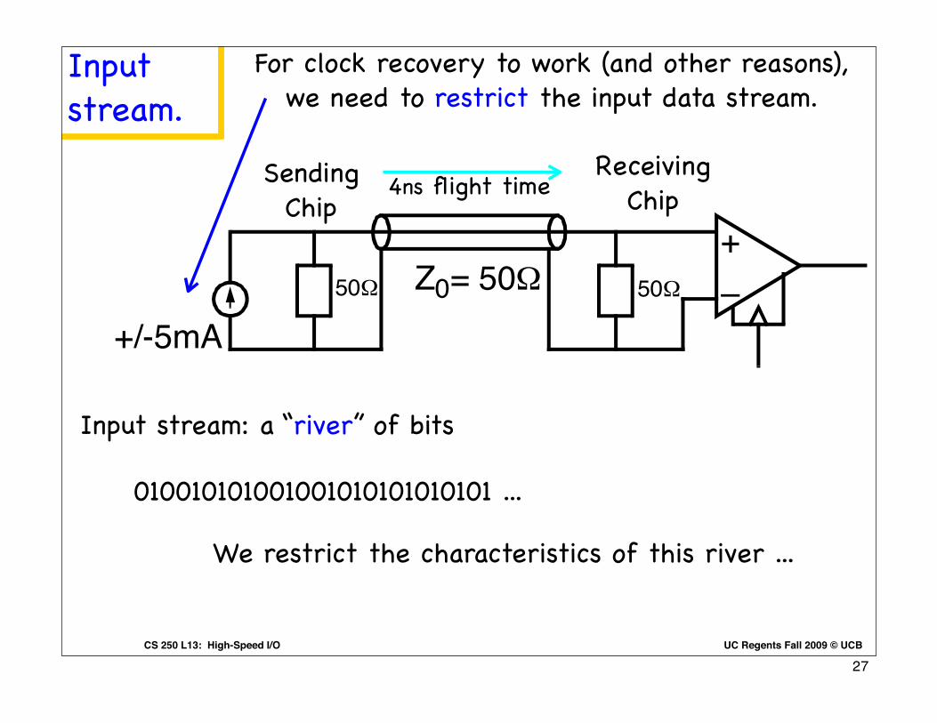
UC Regents Fall 2009 © UCBCS 250 L13: High-Speed I/O
modern microprocessors operate their external buses at
small fraction of their internal clock rate.
Figure 1: A traditional CMOS signaling system.
Figure 1 shows a traditional CMOS signaling system.
CMOS inverters are used as both driver and receiver. The
transmission medium, typically a cable or PC-board trace
has a characteristic impedance of about 50!. The driver
typically has an output impedance of 400! and the line is
unterminated at the receiver. The two power supplies
(VDD = 3.3V and GND = 0V) are used to represent logic 1
and 0 respectively.
The traditional CMOS system is slow because the high
impedance driver is unable to switch the line on the inci-
dent wave. Instead, the driver must ring up the line as the
signal propagates over several round-trips of the line as
shown in Figure 2. The figure shows the voltage as a frac-
tion of VDD at the far end of the line as a function of time.
The incident wave only switches the line to 10% of VDD.
This is doubled by the first reflection at 10ns. Seven tra-
versals of the 4ns line are required to ring the line up to
50% of VDD, and over 15 traversals are needed for the line
to converge to within 10% of its final value.
Figure 2: An 8mA CMOS Driver rings up a 4ns line termi-
nated into 1K!.
The traditional CMOS system is power hungry, dissipat-
ing 1nJ or more to transmit each bit because it requires
large signal swings to overcome poor noise isolation. The
system uses noisy power supplies as transmit and receive
voltage references. It also uses a CMOS inverter which
has both a large offset voltage across process corners (typi-
cally 300mV) and poor sensitivity (about 500mV) as a
receiver. To overcome these noise sources, a large signal
swing, typically the full power supply, is required.
2.2 Low-Swing, Incident-Wave Signaling
A signaling system that overcomes the limitations of
traditional CMOS signaling is shown in Figure 2. A cur-
rent-source transmitter drives the line. A typical drive is
±5mA which gives a 250mV signal swing. The line is ter-
minated at both ends into its characteristic impedance. The
receiver termination absorbs the incident wave preventing
any reflections. The source termination makes the system
more tolerant of crosstalk and impedance discontinuities
by absorbing any ‘stray’ waves that arrive back at the
source. A high-gain clocked regenerative receive amplifier
gives low offset (typically 10mV) and good sensitivity
(10mV or better depending on settling time).
Figure 2: A low-swing, incident-wave signaling system.
By operating using only the incident wave, the system
of Figure 2 can operate at a data rate independent of the
length of the line. A new bit can be driven onto the source
end of the line before the previous bit arrives at the
receiver. As discussed below, this results in a data rate
that, to first approximation, scales linearly with device
speed.
This system operates reliably using a very small voltage
swing (250mV) because it isolates the signal from many
noise sources. Transmit and receive references are isolated
from the noisy power supplies and a clocked receive ampli-
fier greatly improves offset and sensitivity.
3. Limitations on Signaling Rate
The data rate of a signaling system is limited by both the
electronics used to generate and receive the signal and the
medium over which the signal propagates.
3.1 Electronic Limits on Signaling Rate
As illustrated in Figure 3, electronics limits signaling
rate due to rise-time, aperture time, and timing uncertainty
[DP98b]. The time for a bit cell, tbit, must be made long
enough for the signal to slew from one logic level to
another, tr, for the receiver to sample this signal while sta-
ble, ta, and to tolerate jitter between the signal and the sam-
pling clock, 2tu.
All three of these factors are related to the basic time
constant of the semiconductor technology,"n, the time for a
minimum-sized nFET to discharge the gate of an equal-
sized nFET [DP98b]. This time constant is given approxi-
mately by
. (1)
RO= 400! Z0= 50! A=6
0
0.2
0.4
0.6
0.8
0 20 40 60 80
Time (nsec)
Z0= 50!
RO= 50!
+
–
RT= 50!
+/-5mA
"n
VDDCg
IDSS
-----------------=
Input stream.
modern microprocessors operate their external buses at
small fraction of their internal clock rate.
Figure 1: A traditional CMOS signaling system.
Figure 1 shows a traditional CMOS signaling system.
CMOS inverters are used as both driver and receiver. The
transmission medium, typically a cable or PC-board trace
has a characteristic impedance of about 50!. The driver
typically has an output impedance of 400! and the line is
unterminated at the receiver. The two power supplies
(VDD = 3.3V and GND = 0V) are used to represent logic 1
and 0 respectively.
The traditional CMOS system is slow because the high
impedance driver is unable to switch the line on the inci-
dent wave. Instead, the driver must ring up the line as the
signal propagates over several round-trips of the line as
shown in Figure 2. The figure shows the voltage as a frac-
tion of VDD at the far end of the line as a function of time.
The incident wave only switches the line to 10% of VDD.
This is doubled by the first reflection at 10ns. Seven tra-
versals of the 4ns line are required to ring the line up to
50% of VDD, and over 15 traversals are needed for the line
to converge to within 10% of its final value.
Figure 2: An 8mA CMOS Driver rings up a 4ns line termi-
nated into 1K!.
The traditional CMOS system is power hungry, dissipat-
ing 1nJ or more to transmit each bit because it requires
large signal swings to overcome poor noise isolation. The
system uses noisy power supplies as transmit and receive
voltage references. It also uses a CMOS inverter which
has both a large offset voltage across process corners (typi-
cally 300mV) and poor sensitivity (about 500mV) as a
receiver. To overcome these noise sources, a large signal
swing, typically the full power supply, is required.
2.2 Low-Swing, Incident-Wave Signaling
A signaling system that overcomes the limitations of
traditional CMOS signaling is shown in Figure 2. A cur-
rent-source transmitter drives the line. A typical drive is
±5mA which gives a 250mV signal swing. The line is ter-
minated at both ends into its characteristic impedance. The
receiver termination absorbs the incident wave preventing
any reflections. The source termination makes the system
more tolerant of crosstalk and impedance discontinuities
by absorbing any ‘stray’ waves that arrive back at the
source. A high-gain clocked regenerative receive amplifier
gives low offset (typically 10mV) and good sensitivity
(10mV or better depending on settling time).
Figure 2: A low-swing, incident-wave signaling system.
By operating using only the incident wave, the system
of Figure 2 can operate at a data rate independent of the
length of the line. A new bit can be driven onto the source
end of the line before the previous bit arrives at the
receiver. As discussed below, this results in a data rate
that, to first approximation, scales linearly with device
speed.
This system operates reliably using a very small voltage
swing (250mV) because it isolates the signal from many
noise sources. Transmit and receive references are isolated
from the noisy power supplies and a clocked receive ampli-
fier greatly improves offset and sensitivity.
3. Limitations on Signaling Rate
The data rate of a signaling system is limited by both the
electronics used to generate and receive the signal and the
medium over which the signal propagates.
3.1 Electronic Limits on Signaling Rate
As illustrated in Figure 3, electronics limits signaling
rate due to rise-time, aperture time, and timing uncertainty
[DP98b]. The time for a bit cell, tbit, must be made long
enough for the signal to slew from one logic level to
another, tr, for the receiver to sample this signal while sta-
ble, ta, and to tolerate jitter between the signal and the sam-
pling clock, 2tu.
All three of these factors are related to the basic time
constant of the semiconductor technology,"n, the time for a
minimum-sized nFET to discharge the gate of an equal-
sized nFET [DP98b]. This time constant is given approxi-
mately by
. (1)
RO= 400! Z0= 50! A=6
0
0.2
0.4
0.6
0.8
0 20 40 60 80
Time (nsec)
Z0= 50!
RO= 50!
+
–
RT= 50!
+/-5mA
"n
VDDCg
IDSS
-----------------=
4ns flight timeSending Chip
Receiving Chip
For clock recovery to work (and other reasons), we need to restrict the input data stream.
Input stream: a “river” of bits
010010101001001010101010101 ...
We restrict the characteristics of this river ...
27
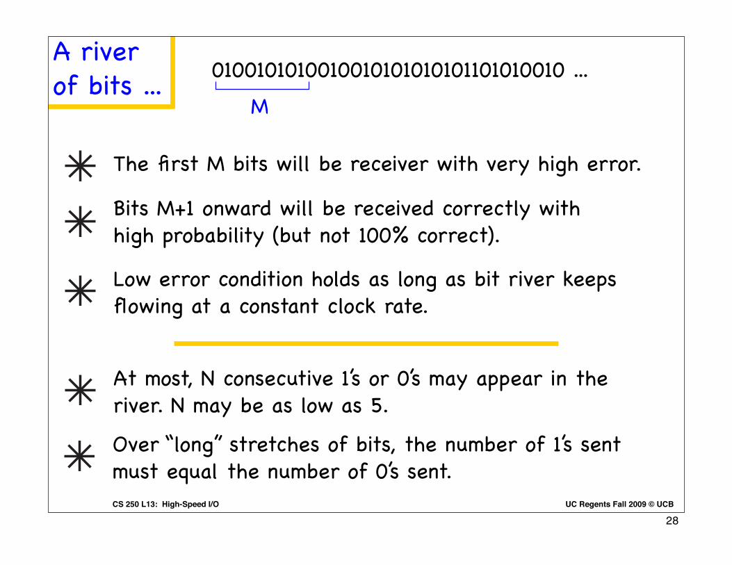
UC Regents Fall 2009 © UCBCS 250 L13: High-Speed I/O
A river of bits ... 0100101010010010101010101101010010 ...
M
The first M bits will be receiver with very high error.
Bits M+1 onward will be received correctly with high probability (but not 100% correct).
Low error condition holds as long as bit river keeps flowing at a constant clock rate.
At most, N consecutive 1’s or 0’s may appear in the river. N may be as low as 5.
Over “long” stretches of bits, the number of 1’s sent must equal the number of 0’s sent.
28

UC Regents Fall 2009 © UCBCS 250 L13: High-Speed I/O
8b/10b codes
Given an arbitrary bitstream, we can code it to have these desired properties.
Example: 8b/10b coding
... 0100101010010010101010101101010010 ...Bits we want to send:
Each 8 bit sequence recoded as 10 bits
... xxxxxxxxxx ...
Recoding algorithm guarantees 0/1 restrictions are met.
Code also offers “out-of-band” 10-bit codes that act as control characters, which higher-level protocols can use to frame the stream, etc.
Does not do error-correction on user data ...29

UC Regents Fall 2009 © UCBCS 250 L13: High-Speed I/O
Next Week : Project Details
Have a good weekend!
30