Crystallization Effects of Nanocrystalline GaN Films on ... · Crystallization Effects of...
6
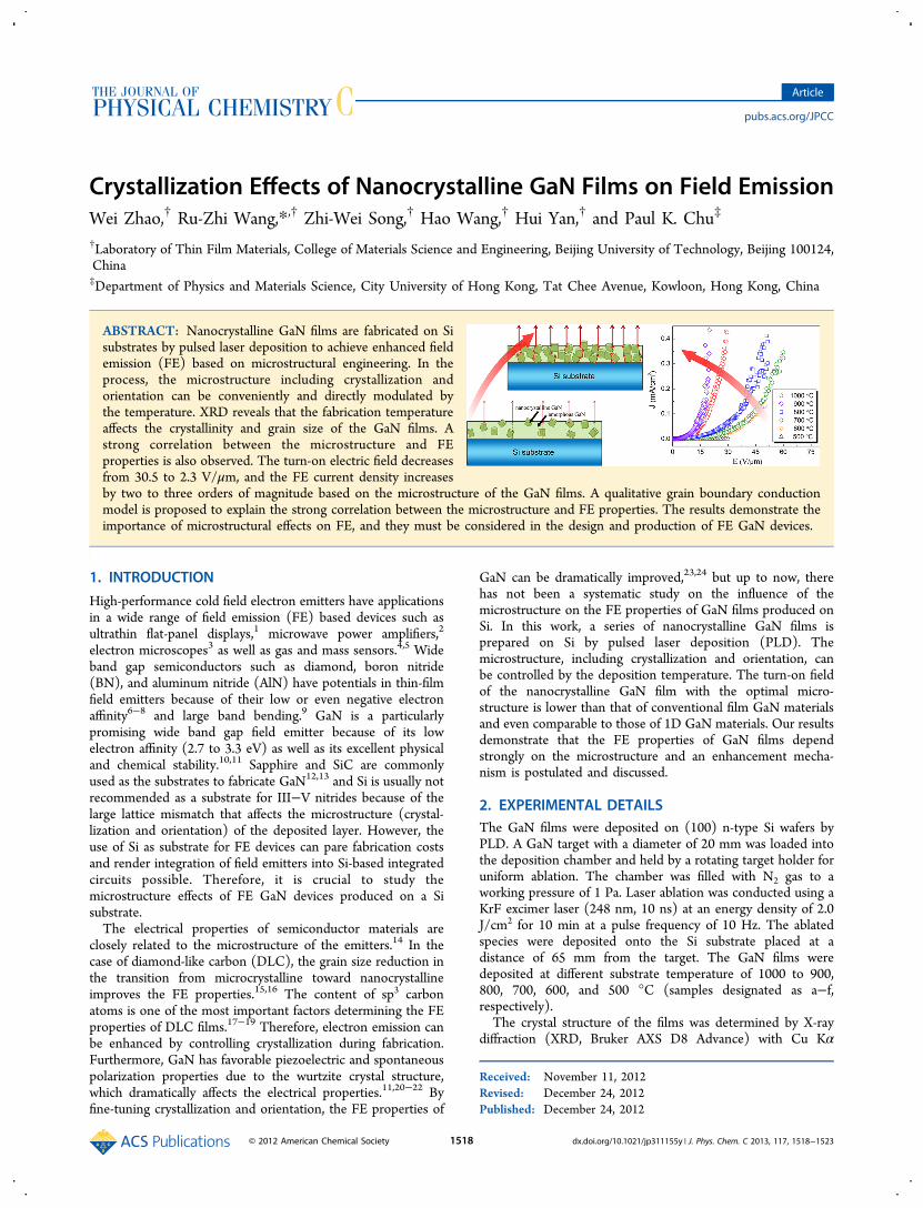
Crystallization Effects of Nanocrystalline GaN Films on Field Emission Wei Zhao, † Ru-Zhi Wang,* ,† Zhi-Wei Song, † Hao Wang, † Hui Yan, † and Paul K. Chu ‡ † Laboratory of Thin Film Materials, College of Materials Science and Engineering, Beijing University of Technology, Beijing 100124, China ‡ Department of Physics and Materials Science, City University of Hong Kong, Tat Chee Avenue, Kowloon, Hong Kong, China ABSTRACT: Nanocrystalline GaN films are fabricated on Si substrates by pulsed laser deposition to achieve enhanced field emission (FE) based on microstructural engineering. In the process, the microstructure including crystallization and orientation can be conveniently and directly modulated by the temperature. XRD reveals that the fabrication temperature affects the crystallinity and grain size of the GaN films. A strong correlation between the microstructure and FE properties is also observed. The turn-on electric field decreases from 30.5 to 2.3 V/μm, and the FE current density increases by two to three orders of magnitude based on the microstructure of the GaN films. A qualitative grain boundary conduction model is proposed to explain the strong correlation between the microstructure and FE properties. The results demonstrate the importance of microstructural effects on FE, and they must be considered in the design and production of FE GaN devices. 1. INTRODUCTION High-performance cold field electron emitters have applications in a wide range of field emission (FE) based devices such as ultrathin flat-panel displays, 1 microwave power amplifiers, 2 electron microscopes 3 as well as gas and mass sensors. 4,5 Wide band gap semiconductors such as diamond, boron nitride (BN), and aluminum nitride (AlN) have potentials in thin-film field emitters because of their low or even negative electron affinity 6-8 and large band bending. 9 GaN is a particularly promising wide band gap field emitter because of its low electron affinity (2.7 to 3.3 eV) as well as its excellent physical and chemical stability. 10,11 Sapphire and SiC are commonly used as the substrates to fabricate GaN 12,13 and Si is usually not recommended as a substrate for III-V nitrides because of the large lattice mismatch that affects the microstructure (crystal- lization and orientation) of the deposited layer. However, the use of Si as substrate for FE devices can pare fabrication costs and render integration of field emitters into Si-based integrated circuits possible. Therefore, it is crucial to study the microstructure effects of FE GaN devices produced on a Si substrate. The electrical properties of semiconductor materials are closely related to the microstructure of the emitters. 14 In the case of diamond-like carbon (DLC), the grain size reduction in the transition from microcrystalline toward nanocrystalline improves the FE properties. 15,16 The content of sp 3 carbon atoms is one of the most important factors determining the FE properties of DLC films. 17-19 Therefore, electron emission can be enhanced by controlling crystallization during fabrication. Furthermore, GaN has favorable piezoelectric and spontaneous polarization properties due to the wurtzite crystal structure, which dramatically affects the electrical properties. 11,20-22 By fine-tuning crystallization and orientation, the FE properties of GaN can be dramatically improved, 23,24 but up to now, there has not been a systematic study on the influence of the microstructure on the FE properties of GaN films produced on Si. In this work, a series of nanocrystalline GaN films is prepared on Si by pulsed laser deposition (PLD). The microstructure, including crystallization and orientation, can be controlled by the deposition temperature. The turn-on field of the nanocrystalline GaN film with the optimal micro- structure is lower than that of conventional film GaN materials and even comparable to those of 1D GaN materials. Our results demonstrate that the FE properties of GaN films depend strongly on the microstructure and an enhancement mecha- nism is postulated and discussed. 2. EXPERIMENTAL DETAILS The GaN films were deposited on (100) n-type Si wafers by PLD. A GaN target with a diameter of 20 mm was loaded into the deposition chamber and held by a rotating target holder for uniform ablation. The chamber was filled with N 2 gas to a working pressure of 1 Pa. Laser ablation was conducted using a KrF excimer laser (248 nm, 10 ns) at an energy density of 2.0 J/cm 2 for 10 min at a pulse frequency of 10 Hz. The ablated species were deposited onto the Si substrate placed at a distance of 65 mm from the target. The GaN films were deposited at different substrate temperature of 1000 to 900, 800, 700, 600, and 500 °C (samples designated as a-f, respectively). The crystal structure of the films was determined by X-ray diffraction (XRD, Bruker AXS D8 Advance) with Cu Kα Received: November 11, 2012 Revised: December 24, 2012 Published: December 24, 2012 Article pubs.acs.org/JPCC © 2012 American Chemical Society 1518 dx.doi.org/10.1021/jp311155y | J. Phys. Chem. C 2013, 117, 1518-1523
Transcript of Crystallization Effects of Nanocrystalline GaN Films on ... · Crystallization Effects of...
Crystallization Effects of Nanocrystalline GaN Films on Field EmissionWei Zhao,† Ru-Zhi Wang,*,† Zhi-Wei Song,† Hao Wang,† Hui Yan,† and Paul K. Chu‡
†Laboratory of Thin Film Materials, College of Materials Science and Engineering, Beijing University of Technology, Beijing 100124,China‡Department of Physics and Materials Science, City University of Hong Kong, Tat Chee Avenue, Kowloon, Hong Kong, China
ABSTRACT: Nanocrystalline GaN films are fabricated on Sisubstrates by pulsed laser deposition to achieve enhanced fieldemission (FE) based on microstructural engineering. In theprocess, the microstructure including crystallization andorientation can be conveniently and directly modulated bythe temperature. XRD reveals that the fabrication temperatureaffects the crystallinity and grain size of the GaN films. Astrong correlation between the microstructure and FEproperties is also observed. The turn-on electric field decreasesfrom 30.5 to 2.3 V/μm, and the FE current density increasesby two to three orders of magnitude based on the microstructure of the GaN films. A qualitative grain boundary conductionmodel is proposed to explain the strong correlation between the microstructure and FE properties. The results demonstrate theimportance of microstructural effects on FE, and they must be considered in the design and production of FE GaN devices.
1. INTRODUCTION
High-performance cold field electron emitters have applicationsin a wide range of field emission (FE) based devices such asultrathin flat-panel displays,1 microwave power amplifiers,2
electron microscopes3 as well as gas and mass sensors.4,5 Wideband gap semiconductors such as diamond, boron nitride(BN), and aluminum nitride (AlN) have potentials in thin-filmfield emitters because of their low or even negative electronaffinity6−8 and large band bending.9 GaN is a particularlypromising wide band gap field emitter because of its lowelectron affinity (2.7 to 3.3 eV) as well as its excellent physicaland chemical stability.10,11 Sapphire and SiC are commonlyused as the substrates to fabricate GaN12,13 and Si is usually notrecommended as a substrate for III−V nitrides because of thelarge lattice mismatch that affects the microstructure (crystal-lization and orientation) of the deposited layer. However, theuse of Si as substrate for FE devices can pare fabrication costsand render integration of field emitters into Si-based integratedcircuits possible. Therefore, it is crucial to study themicrostructure effects of FE GaN devices produced on a Sisubstrate.The electrical properties of semiconductor materials are
closely related to the microstructure of the emitters.14 In thecase of diamond-like carbon (DLC), the grain size reduction inthe transition from microcrystalline toward nanocrystallineimproves the FE properties.15,16 The content of sp3 carbonatoms is one of the most important factors determining the FEproperties of DLC films.17−19 Therefore, electron emission canbe enhanced by controlling crystallization during fabrication.Furthermore, GaN has favorable piezoelectric and spontaneouspolarization properties due to the wurtzite crystal structure,which dramatically affects the electrical properties.11,20−22 Byfine-tuning crystallization and orientation, the FE properties of
GaN can be dramatically improved,23,24 but up to now, therehas not been a systematic study on the influence of themicrostructure on the FE properties of GaN films produced onSi. In this work, a series of nanocrystalline GaN films isprepared on Si by pulsed laser deposition (PLD). Themicrostructure, including crystallization and orientation, canbe controlled by the deposition temperature. The turn-on fieldof the nanocrystalline GaN film with the optimal micro-structure is lower than that of conventional film GaN materialsand even comparable to those of 1D GaN materials. Our resultsdemonstrate that the FE properties of GaN films dependstrongly on the microstructure and an enhancement mecha-nism is postulated and discussed.
2. EXPERIMENTAL DETAILSThe GaN films were deposited on (100) n-type Si wafers byPLD. A GaN target with a diameter of 20 mm was loaded intothe deposition chamber and held by a rotating target holder foruniform ablation. The chamber was filled with N2 gas to aworking pressure of 1 Pa. Laser ablation was conducted using aKrF excimer laser (248 nm, 10 ns) at an energy density of 2.0J/cm2 for 10 min at a pulse frequency of 10 Hz. The ablatedspecies were deposited onto the Si substrate placed at adistance of 65 mm from the target. The GaN films weredeposited at different substrate temperature of 1000 to 900,800, 700, 600, and 500 °C (samples designated as a−f,respectively).The crystal structure of the films was determined by X-ray
diffraction (XRD, Bruker AXS D8 Advance) with Cu Kα
Received: November 11, 2012Revised: December 24, 2012Published: December 24, 2012
Article
pubs.acs.org/JPCC
© 2012 American Chemical Society 1518 dx.doi.org/10.1021/jp311155y | J. Phys. Chem. C 2013, 117, 1518−1523

radiation and X-ray photoelectron spectroscopy (XPS,ESCALAB 250) was applied to examine the surfacecomposition. Atomic force microscopy (AFM, NT-MDTSolver P47) and scanning electron microscopy (SEM, HitachiS4800) were employed to investigate the surface morphology,and the FE properties were determined at room temperatureusing a parallel-plate diode configuration at a pressure of 5 ×10⁻⁷ Pa or lower. A Si wafer (0.001 Ω·cm) was used as theanode, and the cathode and anode (10 × 10 mm2) wereseparated by a glass fiber. The I−V curves were acquired on aKeithley 2410. To remove adsorbates from the cathode surface,the measurements were conducted for several cycles until theJ−E characteristics became stable and reproducible.
3. RESULTS AND DISCUSSIONXPS is used to determine the composition of the samples.Figure 1 shows a general scan in the binding energy range from
0 to 600 eV. The binding energies of the spectra are referencedto that of the C 1s peak (284.8 eV). The nanocrystalline GaNfilm consists of Ga, N, C, and O, and the correspondingphotoelectron peaks are Ga 3d (19.8 eV), Ga 3p (105.4 eV),Ga 3s (159.8 eV), and N 1s (397.6 eV). Because of priorexposure to air, the O 1s and C 1s core level peaks are alsopresent. The insert in Figure 1 shows O 1s and Ga 3d XPSspectra. The O 1s peak at 531.3 eV is attributed to chemisorbedoxygen25 and the Ga 3d core level yields peak positions at 20.6to 20.8 eV for Ga−O bonding and 19.6 to 19.8 eV for Ga−Nbonding.26,27 Therefore, the Ga 3d peak at 19.8 eV can beassigned to nitride. The O 1s and Ga 3d peaks confirm that thesamples are gallium nitride and not oxide.XRD is carried out to determine the crystal structure of the
GaN films. The GaN film deposited at below 500 °C exhibits atypical amorphous pattern. As shown in Figure 2, when thetemperature reaches 600 °C, the characteristic diffraction peaksof GaN begin to appear as a broad peak around 35°. As thetemperature is increased to 800 °C, the peaks at (100), (002),and (101) can be indexed to hexagonal wurtzite GaN,28
indicating the development of a crystalline structure. When thetemperature is further increased to 1000 °C, only the (002)peak can be observed implying that the GaN film ispreferentially oriented in the c-axis direction. The diffractionintensity increases as the deposition temperature is increasedfrom 500 to 1000 °C, indicating that the nanocrystalline GaN
content improves at a higher temperature. The full width athalf-maximum (fwhm) of the (002) peak shows an obviousdrop providing direct evidence that the nanocrystalline GaNgrain size increases at a high substrate temperature. Themodification of crystal structure is attributed to the betterlattice arrangement resulting from increased lattice vibration ata high temperature.To observe the evolution of the GaN films surface
morphology, we show the AFM images of the GaN surfacesin Figure 3. A large quantity of small nanoscale protrusions canbe observed from the surface, and they greatly enhance thelocal electric field.24 As the temperature is increased, thediameter of the surface protrusions decreases from 500 to 100nm, and the corresponding root-mean-square surface roughnessvalues of samples f−a are 50.3, 51.8, 33.6, 16.8, 11.0, and 3.9nm, respectively. XRD and AFM reveal that the depositiontemperature dramatically affects the microstructure and surfacemorphology of the GaN films.The thickness of the GaN films ranges from 220 to 260 nm,
and it may affect the FE characteristics. Zhao et al.29 studied theFE properties of ta-C films with different thicknesses, and athickness-independent phenomenon was observed. However,Lu et al.30 observed that the FE properties of BaSrTiO3 filmwere thickness-dependent. The present study reveals that thefilm-thickness dependence stems from the microstructuralfeatures associated with the different thicknesses. Sugino etal.31 studied the thickness effects of BN nanofilms, and in BNfilms thicker than 20 nm, the turn-on field of the electronemission decreased because of increasing surface roughnessrather than thickness modulation. Hence, it appears that thefilm thickness change alone cannot affect the FE properties oftraditional cathodes thicker than 20 nm. In our experiments,because the films are all thicker than 200 nm, the thicknesseffects can be ignored.The J−E characteristics are shown in Figure 4a, and the
corresponding Fowler−Nordheim (F−N) plots are given inFigure 4b. All samples exhibit a clear FE behavior. The FNplots of all samples in Figure 4b exhibit a linear relationship inthe high-field region, suggesting that the emission currentshould originate from a quantum mechanical tunneling process.In this work, the turn-on field Eon and threshold field Eth aredefined at an emission current density of 1 μA/cm2 and 0.1mA/cm2, respectively. The values of Eon and data from otherGaN nanostructured materials reported previously aresummarized in Table 1. The Eon of the microstructuremodulated nanocrystalline GaN film (sample b) is smaller
Figure 1. XPS spectra of nanocrystalline GaN film. The insert showsthe O 1s and Ga 3d core-level XPS spectra.
Figure 2. XRD pattern obtained from samples b to f. The insert showsthe XRD patterns acquired from sample a.
The Journal of Physical Chemistry C Article
dx.doi.org/10.1021/jp311155y | J. Phys. Chem. C 2013, 117, 1518−15231519

than that of the conventional film GaN materials32−34 and evencomparable to those of 1D GaN materials,28,35−42 indicatingefficient FE from the GaN films with the optimal micro-structure. The detailed information about the F−N plot of GaNfilms is necessary to understand the microstructure effects onfield electron emission.According to the F−N field electron emission theory, the
emission current is related to the applied electric field by thefollowing relationship:43
ϕβ
α βϕ
= − +⎜ ⎟⎛⎝
⎞⎠
⎛⎝⎜
⎞⎠⎟
IV
B dV
Ad
ln ln2
3/2 2
2(1)
where ϕ is the surface effective barrier, d is the distancebetween the anode and cathode, β is the field enhancementfactor, α is the effective emission area, and A and B areconstants corresponding to 1.54 × 10⁻⁶ A(eV)V−2 and 6.83 ×10⁷ (eV)−3/2 V cm−1, respectively. By linear fitting, the field-
enhancement factor and effective emission area can becalculated from the intercept k and slope b of the F−N plot.Because the GaN films are thick enough so that the quantumstructural effects can be neglected24,44−46 and withoutchemisorbed materials, the surface effective barrier ϕ can beconsidered as a constant. If βA and αA are normalized to 1 forsample a, then the field-enhancement factor ratio βr can becalculated from the following relationship:
βββ
ϕϕ
= = · =B dk
kB d
kk
x
A x
A A
xr
2/3
2/3(2)
and the effective emission area ratio αr can be calculated fromthe following
ααα
ϕβ
βϕ β
= = · =b d
A
A
b db
bexp( )
exp( )exp( )
exp( )x
A
x
x
A
A
x
A rr
2
2
2
2 2(3)
Figure 3. AFM images of (a) sample a, (b) sample b, (c) sample c, (d) sample d, (e) sample e, and (f) sample f.
The Journal of Physical Chemistry C Article
dx.doi.org/10.1021/jp311155y | J. Phys. Chem. C 2013, 117, 1518−15231520
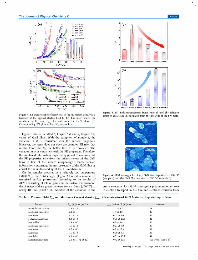
Figure 5 shows the fitted βr (Figure 5a) and αr (Figure 5b)values of GaN films. With the exception of sample f, thevariation in βr is consistent with the surface roughness.However, the result does not obey the common FE rule; thatis, the lower the βr, the better the FE performance. Thevariation in αr is consistent with the FE properties. Therefore,the combined information imparted by βr and αr confirms thatthe FE properties arise from the microstructure of the GaNfilms in lieu of the surface morphology. Hence, detailedinformation concerning the microstructure of the GaN films iscrucial to the understanding of the FE mechanism.On the samples prepared at a relatively low temperature
(<800 °C), the SEM images (Figure 6) reveal a number ofnanosized surface protrusions (according to the results ofAFM) consisting of lots of grains on the surface. Furthermore,the diameter of these grains increases from <10 nm (500 °C) tonearly 100 nm (1000 °C), indicative of the evolution in the
crystal structure. Such GaN nanocrystals play an important rolein electron transport in the film and electrons emission from
Figure 4. FE characteristics of samples a−f: (a) FE current density as afunction of the applied electric field (J−E). The insert shows thevariation in Eon and Eth observed from the GaN films. (b)Corresponding FN plots of ln(I/V2) versus 1/V.
Table 1. Turn-on Field Eon and Maximum Current density Jmax of Nanostructured GaN Materials Reported up to Now
features Eon (V/μm) (μA/cm) Jmax (mA/cm2) (V/μm) reference
triangular microtubes 2.9 at 10 3.0 at 9.5 28needlelike nanowires 2.1 at 1 1.4 at 4.8 40nanowires 4.0 at 10 0.01 at 4.0 37patterned nanowires 8.4 at 10 0.96 at 10.8 42nanocables 1.4 at 0.1 0.1 at 3.4 36needlelike nanowires 7.5 at 10 0.03 at 8.0 39nanowires 8.5 at 0.1 0.2 at 17.5 38nanowires 7.0 at 10 0.09 at 8.3 35nanobelts 6.1 at 0.1 0.35 at 13.5 41nanocrystalline films 2.3 at 1 (6.5 at 10) 0.43 at 20.0 this work (sample b)
Figure 5. (a) Field-enhancement factor ratio βr and (b) effectiveemission areas ratio αr calculated from the linear fit of the FN plots.
Figure 6. SEM micrographs of (a) GaN film deposited at 500 °C(sample f) and (b) GaN film deposited at 700 °C (sample d).
The Journal of Physical Chemistry C Article
dx.doi.org/10.1021/jp311155y | J. Phys. Chem. C 2013, 117, 1518−15231521

the surface; a conducting channel model is proposed to explainelectron transport in the nanocrystalline GaN films.In the interior of the GaN film (Figure 7), the GaN
nanocrystals are embedded in an amorphous GaN matrix. In
the samples fabricated at a low temperature, on account of thesmall grain size and content, the GaN nanocrystals cannotconnect to each other, as shown in Figure 7a. As thetemperature is increased, both the grain size and contentimprove considerably, and connection of separate GaNnanocrystals forms a conducting GaN medium, whichdetermines the electron supply for field electron emission.In general, the FE current can be written as43,47
∫=J e N W E D W W E( , ) ( ) d d(4)
where D(W) is the probability that an electron with energy Wwill penetrate the surface barrier and mainly determined by theeffective surface barrier and field enhancement factor. Thesupply function N(W,E) dW dE is the number of electrons withenergy within the range of E to dE with the z direction of theenergy in the range ofW toW + dW incident on the surface perunit area and time. The electron supply is mainly determinedby electron transport, which can be dramatically affected by themicrostructure of the films.48 In our previous work,24 weproposed that the effective emission area reflected the electrontransport characteristics as well as FE properties. In this work,the combined information imparted by the crystallographiccharacteristics and αr values indicates that the electron supplycan be improved due to the effective conducting pathway.On the basis of the aforementioned analysis, it can be
concluded that the conducting channels depend closely on thenanocrystalline GaN grain size and content. Moreover, theseconducting channels may be caused by two different electrontransport mechanisms that are crucial to the understanding ofthe principles governing the FE enhancement and improve-ment of the FE performance. The first one is electron transportthrough the interior of the nanocrystalline materials.Semenenko et al.48 reported that the Si wires in the SiOx(Si)films led to a high current originating from electron transportthrough these Si wires. Thelander et al.49 observed that the
extended wurtzite segments in zinc blende nanowires had astrong effect on electron transport and increased the resistivityby about two orders of magnitude. Therefore, we suggest thatthe connected GaN nanocrystals embedded in the amorphousGaN matrix act as the effective conduction pathway in whichelectrons can traverse across the GaN films from the interior ofthe conduction channels. However, with regard to sample a,XRD reveals that increasing temperature further improves thecrystallinity and leads to oriented growth in the c-axis direction,thus implying that the nanocrystalline GaN content and grainsize can be dramatically enhanced. As a result, αr is furtherimproved and so are the FE properties, whereas αr and the FEproperties decrease as shown in Figures 4 and 5. It confirmsthat the electron transport does not originate from the interiorof the connected nanocrystalline materials.The second conduction mechanism arises from electron
transport through the grain boundary. A recent study suggestedthat the grain boundary defects introduced localized defectstates.18,50 The evolution of these defect states is thus proposedto be responsible for the high conduction as well as emissionperformance. Herein, compared with sample b, as a result of thenanocrystalline GaN content and grain size being furtherimproved for sample a, the grain boundary and correspondingdefects are dramatically decreased. As a result, electrontransport is suppressed and so is αr in Figure 5b. Hence,grain boundary conduction should be used to explain the originof the FE phenomenon, as shown in Figure 7b. In addition, thegrain size and content can act together or have different signs,thus leading to an additive or subtracting global effect,respectively. The FE properties of GaN can be furtherenhanced by suppression of grain size and improving thenanocrystalline content.
4. CONCLUSIONSThe FE performance of GaN films is improved by micro-structural engineering. A strong correlation between themicrostructure and FE properties of GaN nanocrystals filmsis obtained. The improved nanocrystalline GaN grain size andcontent enhance the electron supply for the FE process. TheFE measurement shows a low turn-on electric field of 2.3 V/μmand yields a stable emission current of 0.43 mA/cm2 at 20 V/μm. The FE performance can be further improved by post-treatment to roughen the surface. However, the effectiveelectron supply is suppressed when the crystallinity improvesfurther. The FE properties of the nanocrystalline GaN films canbe explained by a grain boundary conduction mechanism. Inthis model, the nanocrystalline GaN grain boundary plays animportant role in the electron emitting process, and the resultsprovide insight into the design and fabrication of high-efficiencyFE nanodevices.
■ AUTHOR INFORMATIONCorresponding Author*E-mail: [email protected] authors declare no competing financial interest.
■ ACKNOWLEDGMENTSThe work was financially supported by the National NaturalScience Foundation of China (NSFC) (Grant Nos. 11274029,11074017 and 51032002), the IHLB (Grant No. PHR201007101), the Beijing Nova Program (Grant No.
Figure 7. Models of electron emission from nanocrystalline GaN filmswith (a) small and (b) improved grain size and content.
The Journal of Physical Chemistry C Article
dx.doi.org/10.1021/jp311155y | J. Phys. Chem. C 2013, 117, 1518−15231522

2008B10), the Beijing Natural Science Foundation (Grant No.1102006), the Key Programs of Beijing Plan of Science andTechnology (D121100001812002), Basic Research Foundationof Beijing University of Technology, and Hong Kong ResearchGrants Council (RGC) General Research Funds (GRF) No.CityU 112212.
■ REFERENCES(1) Jeong, H. J.; Jeong, H. D.; Kim, H. Y.; Kim, J. S.; Jeong, S. Y.;Han, J. T.; Bang, D. S.; Lee, G. W. Adv. Funct. Mater. 2011, 21, 1526.(2) Teo, K. B. K.; Minoux, E.; Hudanski, L.; Peauger, F.; Schnell, J.-P.; Gangloff, L.; Legagneux, P.; Dieumegard, D.; Amaratunga, G. A. J.;Milne, W. I. Nature 2005, 437, 968.(3) de Jonge, N.; Lamy, Y.; Schoots, K.; Oosterkamp, T. H. Nature2002, 420, 393.(4) JensenK, K.; ZettlA, K. Nat. Nanotechnol. 2008, 3, 533.(5) Modi, A.; Koratkar, N.; Lass, E.; Wei, B.; Ajayan, P. M. Nature2003, 424, 171.(6) Benjamin, M. C.; Wang, C.; Davis, R. F.; Nemanich, R. J. Appl.Phys. Lett. 1994, 64, 3288.(7) Powers, M. J.; Benjamin, M. C.; Porter, L. M.; Nemanich, R. J.;Davis, R. F.; Cuomo, J. J.; Doll, G. L.; Harris, S. J. Appl. Phys. Lett.1995, 67, 3912.(8) Yamaguchi, H.; Masuzawa, T.; Nozue, S.; Kudo, Y.; Saito, I.; Koe,J.; Kudo, M.; Yamada, T.; Takakuwa, Y.; Okano, K. Phys. Rev. B 2009,80.(9) Wang, R. Z.; Wang, B.; Wang, H.; Zhou, H.; Huang, A. P.; Zhu,M. K.; Yan, H.; Yan, X. H. Appl. Phys. Lett. 2002, 81, 2782.(10) Pankove, J. I.; Schade, H. Appl. Phys. Lett. 1974, 25, 53.(11) Wang, X.; Song, J.; Zhang, F.; He, C.; Hu, Z.; Wang, Z. Adv.Mater. 2010, 22, 2155.(12) Reitmeier, Z. J.; Einfeldt, S.; Davis, R. F.; Zhang, X.; Fang, X.;Mahajan, S. Acta Mater. 2010, 58, 2165.(13) Davis, R. F.; Einfeldt, S.; Preble, E. A.; Roskowski, A. M.;Reitmeier, Z. J.; Miraglia, P. Q. Acta Mater. 2003, 51, 5961.(14) Simon, J.; Protasenko, V.; Lian, C. X.; Xing, H. L.; Jena, D.Science 2010, 327, 60.(15) Joseph, P. T.; Tai, N. H.; Chen, C. H.; Niu, H.; Cheng, H. F.;Palnitkar, U. A.; Lin, I. N. J. Appl. Phys. 2009, 105, 123710.(16) Wang, C. S.; Chen, H. C.; Cheng, H. F.; Lin, I. N. DiamondRelat. Mater. 2009, 18, 136.(17) LeQuan, X. C.; Kang, W. P.; Davidson, J. L.; Choi, B. K.; Wong,Y. M.; Barbosa, R.; Lu, W. Diamond Relat. Mater. 2009, 18, 200.(18) Ikeda, T.; Teii, K. Appl. Phys. Lett. 2009, 94, 143102.(19) Ahmed, S. F.; Moon, M. W.; Lee, K. R. Appl. Phys. Lett. 2008,92, 193502.(20) Fiorentini, V.; Bernardini, F.; Ambacher, O. Appl. Phys. Lett.2002, 80, 1204.(21) Bernardini, F.; Fiorentini, V.; Vanderbilt, D. Phys. Rev. B 1997,56, R10024.(22) Simon, J.; Protasenko, V.; Lian, C.; Xing, H.; Jena, D. Science2010, 327, 60.(23) Zhao, W.; Wang, R. Z.; Han, S.; Xue, K.; Wang, H.; Yan, H. J.Phys. Chem. C 2010, 114, 11584.(24) Zhao, W.; Wang, R. Z.; Song, X. M.; Wang, H.; Wang, B.; Yan,H.; Chu, P. K. Appl. Phys. Lett. 2010, 96, 092101.(25) Li, D.; Sumiya, M.; Fuke, S.; Yang, D.; Que, D.; Suzuki, Y.;Fukuda, Y. J. Appl. Phys. 2001, 90, 4219.(26) Shiozaki, N.; Hashizume, T. J. Appl. Phys. 2009, 105, 064912.(27) Wolter, S. D.; Luther, B. P.; Waltemyer, D. L.; Onneby, C.;Mohney, S. E.; Molnar, R. J. Appl. Phys. Lett. 1997, 70, 2156.(28) Fu, L. T.; Chen, Z. G.; Wang, D. W.; Cheng, L.; Xu, H. Y.; Liu,J. Z.; Cong, H. T.; Lu, G. Q.; Zou, J. J. Phys. Chem. C 2010, 114, 9627.(29) Zhao, J. P.; Chen, Z. Y.; Wang, X.; Shi, T. S.; Yano, T. Appl.Phys. Lett. 2000, 76, 191.(30) Lu, H.; Chen, X. F.; Pan, J. S.; Zhu, W. G. Thin Solid Films 2008,516, 7735.
(31) Sugino, T.; Kimura, C.; Yamamoto, T. Appl. Phys. Lett. 2002, 80,3602.(32) Evtukh, A.; Yilmazoglu, O.; Litovchenko, V.; Semenenko, M.;Gorbanyuk, T.; Grygoriev, A.; Hartnagel, H.; Pavlidis, D. Phys. StatusSolidi C 2008, 5, 425.(33) Deb, P.; Westover, T.; Kim, H.; Fisher, T.; Sands, T. J. Vac. Sci.Technol. B 2007, 25, L15.(34) Sugino, T.; Hori, T.; Kimura, C.; Yamamoto, T. Appl. Phys. Lett.2001, 78, 3229.(35) Liu, B.; Bando, Y.; Tang, C.; Xu, F.; Golberg, D. Appl. Phys. Lett.2005, 87, 073106.(36) Jang, W.; Kim, S.; Lee, J.; Park, J.; Park, C.; Lee, C. Chem. Phys.Lett. 2006, 422, 41.(37) Dinh, D. V.; Kang, S. M.; Yang, J. H.; Kim, S. W.; Yoon, D. H. J.Cryst. Growth. 2009, 311, 495.(38) Ha, B.; Seo, S. H.; Cho, J. H.; Yoon, C. S.; Yoo, J.; Yi, G. C.;Park, C. Y.; Lee, C. J. J. Phys. Chem. B 2005, 109, 11095.(39) Liu, B.; Bando, Y.; Tang, C.; Xu, F.; Hu, J.; Golberg, D. J. Phys.Chem. B 2005, 109, 17082.(40) Lin, C.; Yu, G.; Wang, X.; Cao, M.; Lu, H.; Gong, H.; Qi, M.; Li,A. J Phys Chem C 2008, 112, 18821.(41) Luo, L. Mater. Lett. 2004, 58, 2893.(42) Ng, D. K. T.; Hong, M. H.; Tan, L. S.; Zhu, Y. W.; Sow, C. H.Nanotechnology 2007, 18, 375707.(43) Fowler, R. H.; Nordheim, L. Proc. R. Soc. London, Ser. A 1928,119, 173.(44) Wang, R. Z.; Yan, H.; Wang, B.; Zhang, X. W.; Hou, X. Y. Appl.Phys. Lett. 2008, 92, 142102.(45) Wang, R. Z.; Ding, X. M.; Wang, B.; Xue, K.; Xu, J. B.; Yan, H.;Hou, X. Y. Phys. Rev. B 2005, 72, 125310.(46) Binh, V. T.; Adessi, C. Phys. Rev. Lett. 2000, 85, 864.(47) Young, R. D. Phys. Rev. 1959, 113, 110.(48) Semenenko, M. J. Appl. Phys. 2010, 107, 013702.(49) Thelander, C.; Caroff, P.; Plissard, S. b.; Dey, A. W.; Dick, K. A.Nano Lett. 2011, 11, 2424.(50) Zapol, P.; Sternberg, M.; Curtiss, L. A.; Frauenheim, T.; Gruen,D. M. Phys. Rev. B 2001, 65, 045403.
The Journal of Physical Chemistry C Article
dx.doi.org/10.1021/jp311155y | J. Phys. Chem. C 2013, 117, 1518−15231523