Cryogenic Characterization of Technology for Quantum Computing
4
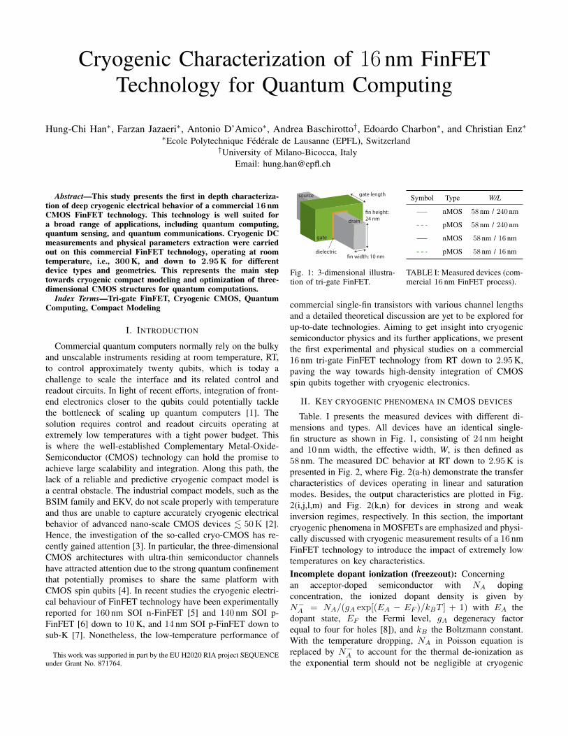
Cryogenic Characterization of 16 nm FinFET Technology for Quantum Computing Hung-Chi Han * , Farzan Jazaeri * , Antonio D’Amico * , Andrea Baschirotto † , Edoardo Charbon * , and Christian Enz * * Ecole Polytechnique F´ ed´ erale de Lausanne (EPFL), Switzerland † University of Milano-Bicocca, Italy Email: hung.han@epfl.ch Abstract—This study presents the first in depth characteriza- tion of deep cryogenic electrical behavior of a commercial 16 nm CMOS FinFET technology. This technology is well suited for a broad range of applications, including quantum computing, quantum sensing, and quantum communications. Cryogenic DC measurements and physical parameters extraction were carried out on this commercial FinFET technology, operating at room temperature, i.e., 300 K, and down to 2.95 K for different device types and geometries. This represents the main step towards cryogenic compact modeling and optimization of three- dimensional CMOS structures for quantum computations. Index Terms—Tri-gate FinFET, Cryogenic CMOS, Quantum Computing, Compact Modeling I. I NTRODUCTION Commercial quantum computers normally rely on the bulky and unscalable instruments residing at room temperature, RT, to control approximately twenty qubits, which is today a challenge to scale the interface and its related control and readout circuits. In light of recent efforts, integration of front- end electronics closer to the qubits could potentially tackle the bottleneck of scaling up quantum computers [1]. The solution requires control and readout circuits operating at extremely low temperatures with a tight power budget. This is where the well-established Complementary Metal-Oxide- Semiconductor (CMOS) technology can hold the promise to achieve large scalability and integration. Along this path, the lack of a reliable and predictive cryogenic compact model is a central obstacle. The industrial compact models, such as the BSIM family and EKV, do not scale properly with temperature and thus are unable to capture accurately cryogenic electrical behavior of advanced nano-scale CMOS devices . 50 K [2]. Hence, the investigation of the so-called cryo-CMOS has re- cently gained attention [3]. In particular, the three-dimensional CMOS architectures with ultra-thin semiconductor channels have attracted attention due to the strong quantum confinement that potentially promises to share the same platform with CMOS spin qubits [4]. In recent studies the cryogenic electri- cal behaviour of FinFET technology have been experimentally reported for 160 nm SOI n-FinFET [5] and 140 nm SOI p- FinFET [6] down to 10 K, and 14 nm SOI p-FinFET down to sub-K [7]. Nonetheless, the low-temperature performance of This work was supported in part by the EU H2020 RIA project SEQUENCE under Grant No. 871764. fin height: 24 nm fin width: 10 nm gate length gate source drain dielectric Fig. 1: 3-dimensional illustra- tion of tri-gate FinFET. Symbol Type W/L nMOS 58 nm / 240 nm pMOS 58 nm / 240 nm nMOS 58 nm / 16 nm pMOS 58 nm / 16 nm TABLE I: Measured devices (com- mercial 16 nm FinFET process). commercial single-fin transistors with various channel lengths and a detailed theoretical discussion are yet to be explored for up-to-date technologies. Aiming to get insight into cryogenic semiconductor physics and its further applications, we present the first experimental and physical studies on a commercial 16 nm tri-gate FinFET technology from RT down to 2.95 K, paving the way towards high-density integration of CMOS spin qubits together with cryogenic electronics. II. KEY CRYOGENIC PHENOMENA IN CMOS DEVICES Table. I presents the measured devices with different di- mensions and types. All devices have an identical single- fin structure as shown in Fig. 1, consisting of 24 nm height and 10 nm width, the effective width, W, is then defined as 58 nm. The measured DC behavior at RT down to 2.95 K is presented in Fig. 2, where Fig. 2(a-h) demonstrate the transfer characteristics of devices operating in linear and saturation modes. Besides, the output characteristics are plotted in Fig. 2(i,j,l,m) and Fig. 2(k,n) for devices in strong and weak inversion regimes, respectively. In this section, the important cryogenic phenomena in MOSFETs are emphasized and physi- cally discussed with cryogenic measurement results of a 16 nm FinFET technology to introduce the impact of extremely low temperatures on key characteristics. Incomplete dopant ionization (freezeout): Concerning an acceptor-doped semiconductor with N A doping concentration, the ionized dopant density is given by N - A = N A /(g A exp[(E A - E F )/k B T ] + 1) with E A the dopant state, E F the Fermi level, g A degeneracy factor equal to four for holes [8]), and k B the Boltzmann constant. With the temperature dropping, N A in Poisson equation is replaced by N - A to account for the thermal de-ionization as the exponential term should not be negligible at cryogenic
Transcript of Cryogenic Characterization of Technology for Quantum Computing
Cryogenic Characterization of 16 nm FinFETTechnology for Quantum Computing
Hung-Chi Han∗, Farzan Jazaeri∗, Antonio D’Amico∗, Andrea Baschirotto†, Edoardo Charbon∗, and Christian Enz∗∗Ecole Polytechnique Federale de Lausanne (EPFL), Switzerland
†University of Milano-Bicocca, ItalyEmail: [email protected]
Abstract—This study presents the first in depth characteriza-tion of deep cryogenic electrical behavior of a commercial 16nmCMOS FinFET technology. This technology is well suited fora broad range of applications, including quantum computing,quantum sensing, and quantum communications. Cryogenic DCmeasurements and physical parameters extraction were carriedout on this commercial FinFET technology, operating at roomtemperature, i.e., 300K, and down to 2.95K for differentdevice types and geometries. This represents the main steptowards cryogenic compact modeling and optimization of three-dimensional CMOS structures for quantum computations.
Index Terms—Tri-gate FinFET, Cryogenic CMOS, QuantumComputing, Compact Modeling
I. INTRODUCTION
Commercial quantum computers normally rely on the bulkyand unscalable instruments residing at room temperature, RT,to control approximately twenty qubits, which is today achallenge to scale the interface and its related control andreadout circuits. In light of recent efforts, integration of front-end electronics closer to the qubits could potentially tacklethe bottleneck of scaling up quantum computers [1]. Thesolution requires control and readout circuits operating atextremely low temperatures with a tight power budget. Thisis where the well-established Complementary Metal-Oxide-Semiconductor (CMOS) technology can hold the promise toachieve large scalability and integration. Along this path, thelack of a reliable and predictive cryogenic compact model isa central obstacle. The industrial compact models, such as theBSIM family and EKV, do not scale properly with temperatureand thus are unable to capture accurately cryogenic electricalbehavior of advanced nano-scale CMOS devices . 50K [2].Hence, the investigation of the so-called cryo-CMOS has re-cently gained attention [3]. In particular, the three-dimensionalCMOS architectures with ultra-thin semiconductor channelshave attracted attention due to the strong quantum confinementthat potentially promises to share the same platform withCMOS spin qubits [4]. In recent studies the cryogenic electri-cal behaviour of FinFET technology have been experimentallyreported for 160 nm SOI n-FinFET [5] and 140 nm SOI p-FinFET [6] down to 10K, and 14 nm SOI p-FinFET down tosub-K [7]. Nonetheless, the low-temperature performance of
This work was supported in part by the EU H2020 RIA project SEQUENCEunder Grant No. 871764.
�n height:24 nm
�n width: 10 nm
gate length
gate
source
drain
dielectric
Fig. 1: 3-dimensional illustra-tion of tri-gate FinFET.
Symbol Type W/L
nMOS 58 nm / 240 nm
pMOS 58 nm / 240 nm
nMOS 58 nm / 16 nm
pMOS 58 nm / 16 nm
TABLE I: Measured devices (com-mercial 16 nm FinFET process).
commercial single-fin transistors with various channel lengthsand a detailed theoretical discussion are yet to be explored forup-to-date technologies. Aiming to get insight into cryogenicsemiconductor physics and its further applications, we presentthe first experimental and physical studies on a commercial16 nm tri-gate FinFET technology from RT down to 2.95K,paving the way towards high-density integration of CMOSspin qubits together with cryogenic electronics.
II. KEY CRYOGENIC PHENOMENA IN CMOS DEVICES
Table. I presents the measured devices with different di-mensions and types. All devices have an identical single-fin structure as shown in Fig. 1, consisting of 24 nm heightand 10 nm width, the effective width, W, is then defined as58 nm. The measured DC behavior at RT down to 2.95K ispresented in Fig. 2, where Fig. 2(a-h) demonstrate the transfercharacteristics of devices operating in linear and saturationmodes. Besides, the output characteristics are plotted in Fig.2(i,j,l,m) and Fig. 2(k,n) for devices in strong and weakinversion regimes, respectively. In this section, the importantcryogenic phenomena in MOSFETs are emphasized and physi-cally discussed with cryogenic measurement results of a 16 nmFinFET technology to introduce the impact of extremely lowtemperatures on key characteristics.Incomplete dopant ionization (freezeout): Concerningan acceptor-doped semiconductor with NA dopingconcentration, the ionized dopant density is given byN−
A = NA/(gA exp[(EA − EF )/kBT ] + 1) with EA thedopant state, EF the Fermi level, gA degeneracy factorequal to four for holes [8]), and kB the Boltzmann constant.With the temperature dropping, NA in Poisson equation isreplaced by N−
A to account for the thermal de-ionization asthe exponential term should not be negligible at cryogenic
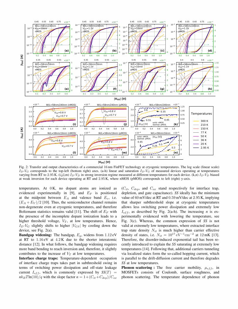
Fig. 2: Transfer and output characteristics of a commercial 16 nm FinFET technology at cryogenic temperatures. The log scale (linear scale)ID-VG corresponds to the top-left (bottom right) axes. (a-h) linear and saturation ID-VG of measured devices operating at temperaturesvarying from RT to 2.95K. (i,j,l,m) ID-VD in strong inversion regime measured at different temperatures for each device. (k,n) ID-VD biasedat weak inversion for each device operating at RT and 2.95K, where nMOS (pMOS) corresponds to left (right) y-axis.
temperatures. At 0K, no dopant atoms are ionized asevidenced experimentally in [9], and EF is positionedat the midpoint between EA and valence band Ev , i.e.(EA +EV )/2 [10]. Thus, the semiconductor channel remainsnon-degenerate even at cryogenic temperatures, and thereforeBoltzmann statistics remains valid [11]. The shift of EF withthe presence of the incomplete dopant ionization leads to ahigher threshold voltage, VT , at low temperatures. Hence,ID-VG slightly shifts to higher |VGS | by cooling down thedevice, see Fig. 2(a).Bandgap widening: The bandgap, Eg , widens from 1.12 eVat RT to 1.16 eV at 4.2K due to the shorter interatomicdistance [12]. In what follows, the bandgap widening requiresmore band bending to reach inversion and, therefore, it slightlycontributes to the increase of VT at low temperatures.Interface charge traps: Temperature-dependent occupationof interface charge traps takes part in subthreshold swing interms of switching power dissipation and off-state leakagecurrent Ioff , which is commonly expressed by SS(T ) =nkBT ln(10)/q with the slope factor n = 1+(Cit+Cdep)/Cox
(Cit, Cdep, and Cox stand respectively for interface trap,depletion, and gate capacitance). SS ideally has the minimumvalue of 60mV/dec at RT and 0.59mV/dec at 2.95K, implyingthat sharper subthreshold slope at cryogenic temperaturesallows less switching power dissipation and extremely lowIoff , as described by Fig. 2(a-h). The increasing n is ex-perimentally evidenced with lowering the temperature, seeFig. 3(c). Whereas, the common expression of SS is notvalid at extremely low temperatures, where extracted interfacetrap state density Nit is much higher than carrier effectivedensity of states, i.e. Nit = 1017 eV−1cm−2 at 12mK [13].Therefore, the disorder-induced exponential tail has been re-cently introduced to explain the SS saturating at extremely lowtemperatures [14]. Following that, additional carriers tunnelingvia localized states form the so-called hopping current, whichis parallel to the drift-diffusion current and therefore degradesSS at low temperatures.Phonon scattering : The free carrier mobility, µeff , inMOSFETs consists of Coulomb, surface roughness, andphonon scattering. The temperature dependence of phonon
10 11 10 10 10 9 10 8 10 7 10 6
ISD [A]
0
20
40
60
80
100dV
SG/d
(logI
SD) [
mV/
dec] W/L=58nm/240nm (pMOS)
|VDS| = 1.1 V
(a)
2.95 K36 K
77 K300 K
3 20 36 50 77 300
T [K]
610
20
4060
100
SS [m
V/de
c] |VDS| = 1.1 V
L=240 nm
L=16 nm
(b)
UTln(10)
3 20 36 50 77 300
T [K]
1246
102030
n
|VDS|=1.1 V
L=240 nm
L=16 nm
(c)
T [K]
0.35
0.40
0.45
0.50
0.55
0.60
V T [V
]
|VDS|=1.1 V
L=240 nm
L=16 nm
(d)
3 36 77 150 210 300
T [K]
0.00
0.02
0.04
0.06
0.08
0.10
DIBL
L=240 nm
L=16 nm
(e)
0.05 0.10 0.15 0.20 0.25 0.30 0.35 0.40 0.45
VOV [V]
5
10
15
effC
ox [m
F/Vs
] W/L=58nm/240nm (nMOS)
VDS=10 mV
T
(f)
3 36 77 150 210 300
T [K]
1
2
3
4
eff /
ef
fat
300K
Vov, interp=0.2 V|VDS|=10 mV
nMOSpMOS
(g)
0.0
0.5
1.0
1.5
2.0
2.5
3.0
Go [
S]
W/L=58nm/240nm|VGS|=0.8 V nMOS
(h)
3 36 77 150 210 300
T [K]
5.5
6.0
6.5
7.0
7.5
Go [
S]
W/L=58nm/16nm|VGS|=0.8 V
nMOS(i)
0.05
0.10
0.15
0.20
0.25
0.30
pMOS
9.5
10.0
10.5
11.0pMOS
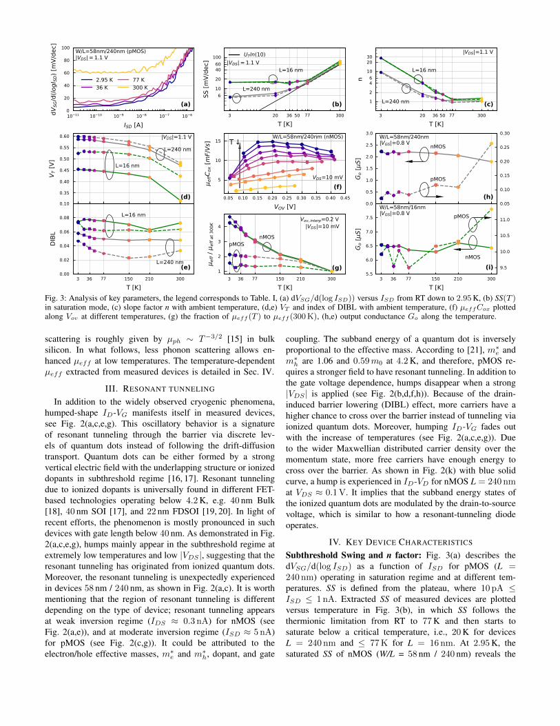
Fig. 3: Analysis of key parameters, the legend corresponds to Table. I, (a) dVSG/d(log ISD)) versus ISD from RT down to 2.95K, (b) SS(T )in saturation mode, (c) slope factor n with ambient temperature, (d,e) VT and index of DIBL with ambient temperature, (f) µeffCox plottedalong Vov at different temperatures, (g) the fraction of µeff (T ) to µeff (300K), (h,e) output conductance Go along the temperature.
scattering is roughly given by µph ∼ T−3/2 [15] in bulksilicon. In what follows, less phonon scattering allows en-hanced µeff at low temperatures. The temperature-dependentµeff extracted from measured devices is detailed in Sec. IV.
III. RESONANT TUNNELING
In addition to the widely observed cryogenic phenomena,humped-shape ID-VG manifests itself in measured devices,see Fig. 2(a,c,e,g). This oscillatory behavior is a signatureof resonant tunneling through the barrier via discrete lev-els of quantum dots instead of following the drift-diffusiontransport. Quantum dots can be either formed by a strongvertical electric field with the underlapping structure or ionizeddopants in subthreshold regime [16, 17]. Resonant tunnelingdue to ionized dopants is universally found in different FET-based technologies operating below 4.2K, e.g. 40 nm Bulk[18], 40 nm SOI [17], and 22 nm FDSOI [19, 20]. In light ofrecent efforts, the phenomenon is mostly pronounced in suchdevices with gate length below 40 nm. As demonstrated in Fig.2(a,c,e,g), humps mainly appear in the subthreshold regime atextremely low temperatures and low |VDS |, suggesting that theresonant tunneling has originated from ionized quantum dots.Moreover, the resonant tunneling is unexpectedly experiencedin devices 58 nm / 240 nm, as shown in Fig. 2(a,c). It is worthmentioning that the region of resonant tunneling is differentdepending on the type of device; resonant tunneling appearsat weak inversion regime (IDS ≈ 0.3 nA) for nMOS (seeFig. 2(a,e)), and at moderate inversion regime (ISD ≈ 5 nA)for pMOS (see Fig. 2(c,g)). It could be attributed to theelectron/hole effective masses, m∗
e and m∗h, dopant, and gate
coupling. The subband energy of a quantum dot is inverselyproportional to the effective mass. According to [21], m∗
e andm∗
h are 1.06 and 0.59m0 at 4.2K, and therefore, pMOS re-quires a stronger field to have resonant tunneling. In addition tothe gate voltage dependence, humps disappear when a strong|VDS | is applied (see Fig. 2(b,d,f,h)). Because of the drain-induced barrier lowering (DIBL) effect, more carriers have ahigher chance to cross over the barrier instead of tunneling viaionized quantum dots. Moreover, humping ID-VG fades outwith the increase of temperatures (see Fig. 2(a,c,e,g)). Dueto the wider Maxwellian distributed carrier density over themomentum state, more free carriers have enough energy tocross over the barrier. As shown in Fig. 2(k) with blue solidcurve, a hump is experienced in ID-VD for nMOS L = 240 nmat VDS ≈ 0.1V. It implies that the subband energy states ofthe ionized quantum dots are modulated by the drain-to-sourcevoltage, which is similar to how a resonant-tunneling diodeoperates.
IV. KEY DEVICE CHARACTERISTICS
Subthreshold Swing and n factor: Fig. 3(a) describes thedVSG/d(log ISD) as a function of ISD for pMOS (L =240 nm) operating in saturation regime and at different tem-peratures. SS is defined from the plateau, where 10 pA ≤ISD ≤ 1 nA. Extracted SS of measured devices are plottedversus temperature in Fig. 3(b), in which SS follows thethermionic limitation from RT to 77K and then starts tosaturate below a critical temperature, i.e., 20K for devicesL = 240 nm and ≤ 77K for L = 16nm. At 2.95K, thesaturated SS of nMOS (W/L = 58 nm / 240 nm) reveals the

deviation between experimental (5.2mV/dec) and theoreticalvalues (0.6mV/dec), leading to n factor rise up to ≈ 9, asshown in Fig. 3(c). Whereas, SS is 18mV/dec at 2.95K forsuch devices with L = 16nm, which dramatically raises then factor to ≈ 30, as shown in Fig. 3(c). Comparing the darkblue lines from Fig. 2(g) and Fig. 2(h), SS is degraded more ina short device operating in saturation regime and at cryogenictemperatures. The degradation in SS is likely due to the source-to-drain tunneling current [22], which starts to dominate thesubthreshold current at 77 K for L = 16nm.Threshold Voltage: The linear extrapolation method is uti-lized for extracting VT ; VT is defined by the extrapolation froma region of ID-VG where the maximum transconductance,max(Gm), is reached. Extracted threshold voltages from Fig.2(b,d,f,h) are plotted versus temperature in Fig. 3(d). Anincreasing and saturating VT is experienced with the fall oftemperatures; the VT at 2.95K is overall higher than that atRT by 120mV. The phenomenon is mainly attributed to theshifted EF with the presence of incomplete dopant ionizationand bandgap widening. DIBL is described as a function oftemperature in Fig. 3(e). Devices with 16 nm gate lengthsshow stronger DIBL over temperatures. It is worth notingthat the impact of DIBL can be clearly observed from outputcharacteristic of pMOS with L = 16nm at 2.95K (see dashedblue line in Fig. 2(n)).Free carrier mobility: The gDS function by Jazaeri et al.is used to extract low-field free carrier mobility, µeff inFETs [23]. This approach relies on drift-diffusion trans-port without assuming any gate-voltage-mobility dependence.µeff is expressed by µeff ' −(2L/WCox)(∂gDS/∂VDS)and is only used within strong inversion and linear regimes.Fig. 3(f) demonstrates µeffCox versus the overdrive voltage,Vov , at different temperatures, where cryogenic temperatureallows lower phonon scattering assuming Cox is temperature-independent. At temperatures below 36K, µeffCox reachesa maximum at Vov ≈ 0.15V and then decreases at higherVov (stronger normal effective field), where the degradationof mobility is due to the dominance of the surface roughnessscattering [24]. Fig. 3(g) reveals a ratio of µeff (normalizedto the room-temperature µeff ) versus temperature with Vov ≈0.2V. Electron µeff at 2.95K is enhanced by > 4 times incomparison to that at RT. Besides, it does not show significantdifference between devices with L = 16 and 240 nm. However,hole µeff is only increased by 2.2 and 1.5 times for pMOSdevices with L = 240 and 16 nm, respectively.Output conductance: Output conductance, Go, obtainedfrom saturation ID-VD is roughly proportional to inversioncharge density and mobility, which are competing as thetemperature decreased. As evidenced by Fig. 3(h,i), Go(T )at constant |VGS | = 0.8V does not show a significantdependence on temperature for nMOS. Whereas, Go of pMOSslightly decrease at cryogenic temperatures owing to lessenhancement to the free hole mobility.
V. CONCLUSION
We present the first cryogenic characterization of differentdevice types and geometries from a commercial 16 nm FinFETtechnology. The important low-temperature effects on CMOSdevices are shown and discussed in this work in terms ofSS, VT , and µeff . Besides, the additional carrier transportmechanisms, resonant tunneling and source-to-drain tunneling,are observed at cryogenic temperatures.
REFERENCES
[1] E. Charbon, F. Sebastiano et al., “Cryo-CMOS for quantum computing,”in IEDM, Dec. 2016, pp. 13.5.1–13.5.4.
[2] A. Akturk, M. Holloway et al., “Compact and distributed modeling ofcryogenic bulk MOSFET operation,” IEEE TED, vol. 57, no. 6, pp.1334–1342, Jun. 2010.
[3] C. Enz, A. Beckers, and F. Jazaeri, “Cryo-CMOS Compact Modeling,”in IEDM, Dec. 2020, pp. 1–25.
[4] F. Jazaeri, A. Beckers et al., “A Review on quantum computing:From qubits to front-end electronics and cryogenic mosfet physics,” inMIXDES, Jun. 2019, pp. 15–25.
[5] H. Achour, B. Cretu et al., “Detailled characterisation of SOI n-FinFETsat very low temperature,” in ULIS, Mar. 2013, pp. 125–128.
[6] H. Achour, R. Talmat et al., “DC and low frequency noise performancesof SOI p-FinFETs at very low temperature,” SSE, vol. 90, pp. 160–165,Dec. 2013.
[7] O. Lopez-L, I. Martınez et al., “Electrical and thermal characterizationfor soi p-type finfet down to sub-kelvin temperatures,” in LAEDC, 2020,pp. 1–3.
[8] S. Sze and K. K. Ng, Physics of Semiconductor Devices. John Wiley& Sons, Inc., 2006.
[9] M. Rudan, Physics of Semiconductor Devices. Springer New York,2015.
[10] R. F. Pierret, Advanced semiconductor fundamentals. Pearson Educa-tion, 2003.
[11] A. Beckers, F. Jazaeri, and C. Enz, “Cryogenic MOS Transistor Model,”IEEE TED, vol. 65, no. 9, pp. 3617–3625, 2018.
[12] Y. P. Varshni, “Temperature dependence of the energy gap in semicon-ductors,” Physica, vol. 34, no. 1, pp. 149–154, Jan. 1967.
[13] P. Galy, J. Camirand Lemyre et al., “Cryogenic Temperature Characteri-zation of a 28-nm FD-SOI Dedicated Structure for Advanced CMOS andQuantum Technologies Co-Integration,” IEEE JEDS, vol. 6, pp. 594–600, May 2018.
[14] A. Beckers, F. Jazaeri, and C. Enz, “Theoretical Limit of Low Tem-perature Subthreshold Swing in Field-Effect Transistors,” IEEE EDL,vol. 41, no. 2, pp. 276–279, 2020.
[15] M. Lundstrom, Fundamentals of Carrier Transport. Cambridge Uni-versity Press, Oct. 2010.
[16] R. Wacquez, M. Vinet et al., “Single dopant impact on electricalcharacteristics of SOI NMOSFETs with effective length down to 10nm,”VLSIT, pp. 193–194, 2010.
[17] Y. Ono, K. Nishiguchi et al., “Conductance modulation by individualacceptors in Si nanoscale field-effect transistors,” APL, vol. 90, no. 10,2007.
[18] P. A. ’T Hart, M. Babaie et al., “Characterization and modeling ofmismatch in cryo-cmos,” IEEE JEDS, vol. 8, pp. 263–273, 2020.
[19] S. Bonen, U. Alakusu et al., “Cryogenic characterization of 22-nmFDSOI CMOS technology for quantum computing ICs,” IEEE EDL,vol. 40, no. 1, pp. 127–130, 2019.
[20] A. Beckers, F. Jazaeri et al., “Characterization and modeling of 28-nmFDSOI CMOS technology down to cryogenic temperatures,” SSE, vol.159, pp. 106–115, 2019.
[21] M. A. Green, “Intrinsic concentration, effective densities of states, andeffective mass in silicon,” J. Appl. Phys, vol. 67, no. 6, pp. 2944–2954,Mar. 1990.
[22] J. Wang and M. Lundstrom, “Does source-to-drain tunneling limit theultimate scaling of MOSFETs?” in IEDM, 2002, pp. 707–710.
[23] F. Jazaeri, A. Pezzotta, and C. Enz, “Free Carrier Mobility Extractionin FETs,” IEEE TED, vol. 64, no. 12, pp. 5279–5283, Dec. 2017.
[24] S.-i. Takagi, A. Toriumi et al., “On the Universality of InversionLayer Mobility in Si MOSFET’s: Part I—Effects of Substrate ImpurityConcentration,” IEEE TED, vol. 41, no. 12, pp. 2357–2362, 1994.


![Quantum Non-Markovianity: Characterization, Quantification ...arXiv:1405.0303v2 [quant-ph] 24 Aug 2014 REVIEW ARTICLE Quantum Non-Markovianity: Characterization, Quantification and](https://static.fdocuments.net/doc/165x107/5f686450aac7fc0d604af5b8/quantum-non-markovianity-characterization-quantiication-arxiv14050303v2.jpg)