CrossLink High-Speed I/O MIPI D-PHY and DDR Interfaces
61
CrossLink High-Speed I/O MIPI D-PHY and DDR Interfaces Preliminary Technical Note FPGA-TN-02012 Version 1.1 July 2016
Transcript of CrossLink High-Speed I/O MIPI D-PHY and DDR Interfaces

CrossLink High-Speed I/O MIPI D-PHY and DDR Interfaces
Preliminary Technical Note
FPGA-TN-02012 Version 1.1
July 2016

CrossLink High-Speed I/O MIPI D-PHY and DDR Interfaces Preliminary Technical Note
© 2015-2016 Lattice Semiconductor Corp. All Lattice trademarks, registered trademarks, patents, and disclaimers are as listed at www.latticesemi.com/legal. All other brand or product names are trademarks or registered trademarks of their respective holders. The specifications and information herein are subject to change without notice.
2 FPGA-TN-02012-1.1
Contents Acronyms in This Document ................................................................................................................................................. 5 1. Introduction .................................................................................................................................................................. 6 2. MIPI D-PHY Interface .................................................................................................................................................... 6 3. High-Speed External Interface ...................................................................................................................................... 7 4. General Purpose High-Speed Interface Building Blocks ............................................................................................... 8
4.1. Edge Clocks .......................................................................................................................................................... 8 4.2. Primary Clocks ..................................................................................................................................................... 8 4.3. PLL ....................................................................................................................................................................... 8 4.4. DDRDLL ................................................................................................................................................................ 8 4.5. DLLDEL ................................................................................................................................................................. 8 4.6. Input DDR ............................................................................................................................................................ 8 4.7. Output DDR ......................................................................................................................................................... 9 4.8. Edge Clock Dividers (CLKDIV) .............................................................................................................................. 9 4.9. Input/Output DELAY ............................................................................................................................................ 9
5. High-Speed DDR Interface Details .............................................................................................................................. 10 5.1. Types of High-Speed DDR Interfaces ................................................................................................................. 10 5.2. Generic DDR Receive Interfaces ........................................................................................................................ 11
5.2.1. GDDRX1_RX.SCLK.Centered ......................................................................................................................... 11 5.2.2. GDDRX1_RX.SCLK.Aligned ............................................................................................................................ 13 5.2.3. GDDRX2_RX.ECLK.Centered (1:4 Gearing), GDDRX4_RX.ECLK.Centered (1:8 Gearing) and
GDDRX8_RX.ECLK.Centered (1:16 Gearing) ................................................................................................. 15 5.2.4. GDDRX2_RX.ECLK.Aligned (1:4 Gearing), GDDRX4_RX.ECLK.Aligned (1:8 Gearing) and
GDDRX8_RX.ECLK.Aligned (1:16 Gearing) .................................................................................................... 16 5.3. 7:1 LVDS Receive Interfaces .............................................................................................................................. 18
5.3.1. GDDRX71_RX.ECLK (1:7 Gearing) and GDDRX141_RX.ECLK (1:14 Gearing) ................................................. 18 5.4. MIPI D-PHY Receive Interfaces .......................................................................................................................... 22
5.4.1. MIPI DSI Receive Interface – Soft D-PHY Module ......................................................................................... 22 5.4.2. MIPI CSI2 Receive Interface – Soft D-PHY Module ....................................................................................... 24 5.4.3. MIPI DSI Receive Interface – Hard D-PHY Module ....................................................................................... 26 5.4.4. MIPI CSI-2 Receive Interface – Hard D-PHY Module .................................................................................... 28
5.5. Generic DDR Transmit Interfaces ...................................................................................................................... 31 5.5.1. GDDRX1_TX.SCLK.Aligned (2:1 Gearing)....................................................................................................... 31 5.5.2. GDDRX1_TX.SCLK.Centered (2:1 Gearing) .................................................................................................... 33 5.5.3. GDDRX2_TX.ECLK.Aligned (4:1 Gearing), GDDRX4_TX.ECLK.Aligned (8:1 Gearing) and
GDDRX8_TX.ECLK.Aligned (16:1 Gearing) .................................................................................................... 34 5.5.4. GDDRX2_TX.ECLK.Centered (4:1 Gearing), GDDRX4_TX.ECLK.Centered (8:1 Gearing) and
GDDRX8_TX.ECLK. Centered (16:1 Gearing) ................................................................................................. 36 5.6. 7:1 LVDS Transmit Interfaces ............................................................................................................................ 38
5.6.1. GDDRX71_TX.ECLK (7:1 Gearing) and GDDRX141_TX.ECLK (14:1 Gearing) ................................................. 38 5.7. MIPI D-PHY Transmit Interfaces ........................................................................................................................ 39
5.7.1. MIPI DSI Transmit Interface – Hard D-PHY Module ...................................................................................... 39 5.7.2. MIPI CSI-2 Transmit Interface – Hard D-PHY Module ................................................................................... 42
6. Using Clarity to Build High-Speed I/O Interfaces ........................................................................................................ 45 6.1. Configuring High-Speed I/O Interfaces in Clarity Designer ............................................................................... 45 6.2. Building DDR Generic Modules ......................................................................................................................... 45 6.3. Building 7:1 LVDS Interface Modules ................................................................................................................ 50 6.4. Building MIPI D-PHY Interface Modules ............................................................................................................ 51 6.5. Building SDR Modules ....................................................................................................................................... 53 6.6. Receive Interface Guidelines ............................................................................................................................. 54 6.7. Transmit Interface Guidelines ........................................................................................................................... 55 6.8. Clocking Guidelines for Generic DDR Interface ................................................................................................. 55 6.9. Timing Analysis for High-Speed DDR Interfaces ................................................................................................ 55

CrossLink High-Speed I/O MIPI D-PHY and DDR Interfaces Preliminary Technical Note
© 2015-2016 Lattice Semiconductor Corp. All Lattice trademarks, registered trademarks, patents, and disclaimers are as listed at www.latticesemi.com/legal. All other brand or product names are trademarks or registered trademarks of their respective holders. The specifications and information herein are subject to change without notice.
FPGA-TN-02012-1.1 3
6.9.1. Frequency Constraints.................................................................................................................................. 55 6.9.2. DDR Input Setup and Hold Time Constraints ............................................................................................... 56 6.9.3. DDR Clock to Out Constraints for Transmit Interfaces ................................................................................. 57
References .......................................................................................................................................................................... 60 Technical Support Assistance ............................................................................................................................................. 60 Revision History .................................................................................................................................................................. 60
Figures
Figure 3.1. External Interface Definitions ............................................................................................................................. 7 Figure 5.1. GDDRX1_RX.SCLK.Centered Interface (Static Delay) ........................................................................................ 12 Figure 5.2. GDDRX1_RX.SCLK.Centered Interface (Dynamic Data Delay) ........................................................................... 12 Figure 5.3. GDDRX1_RX.SCLK.Aligned Interface (Static Data Delay) .................................................................................. 13 Figure 5.4. GDDRX1_RX.SCLK.Aligned Interface (Dynamic Data/Clock Delay) ................................................................... 14 Figure 5.5. GDDRX2_RX.ECLK.Centered Interface (Static Delay) ........................................................................................ 15 Figure 5.6. GDDRX2_RX.ECLK.Centered Interface (Static Delay) with GDDR_SYNC Soft IP ................................................ 15 Figure 5.7. GDDRX2_RX.ECLK.Centered Interface (Dynamic Data Delay) without GDDR_SYNC Soft IP ............................. 16 Figure 5.8. GDDRX2_RX.ECLK.Aligned Interface (Static Delay) with RXDLL_SYNC IP ......................................................... 17 Figure 5.9. GDDRX2_RX.ECLK.Aligned Interface (Dynamic Data/Clock Delay) ................................................................... 17 Figure 5.10. GDDRX71_RX.ECLK Interface (DELAYF and BW_ALIGN not enabled) ............................................................. 19 Figure 5.11. GDDRX71_RX.ECLK Interface with GDDR_SYNC and BW_ALIGN Soft IP ........................................................ 20 Figure 5.12. GDDRX71_RX.ECLK Interface with GDDR_SYNC, BW_ALIGN Soft IP and DELAYF Tuning .............................. 20 Figure 5.13. GDDRX141_RX.ECLK Interface with GDDR_SYNC, BW_ALIGN and DELAYF Tuning Soft IP ............................ 21 Figure 5.14. MIPI DSI Receive Interface with Soft D-PHY Module ...................................................................................... 23 Figure 5.15. MIPI CSI-2 Receive Interface with Soft D-PHY Module ................................................................................... 25 Figure 5.16. MIPI DSI Receive Interface with Hard D-PHY Module .................................................................................... 27 Figure 5.17. MIPI CSI2 Receive Interface with Hard D-PHY Module ................................................................................... 30 Figure 5.18. GDDRX1_TX.SCLK.Aligned Interface ............................................................................................................... 32 Figure 5.19. GDDRX1_TX.SCLK.Aligned Interface (with Registered Tristate and Optional Dynamic Data Delay) .............. 32 Figure 5.20. GDDRX1_TX.SCLK.Centered Interface ............................................................................................................ 33 Figure 5.21. GDDRX1_TX.SCLK.Centered Interface (with Registered Tristate and Optional Dynamic Delay) .................... 34 Figure 5.22. GDDRX2_TX.ECLK.Aligned Interface ............................................................................................................... 35 Figure 5.23. GDDRX2_TX.ECLK.Aligned Interface (with Registered Tristate) ..................................................................... 35 Figure 5.24. GDDRX2_TX.ECLK.Centered Interface ............................................................................................................ 37 Figure 5.25. GDDRX2_TX.ECLK.Centered Interface (with Registered Tristate) ................................................................... 37 Figure 5.26. GDDRX71_TX.ECLK Interface .......................................................................................................................... 38 Figure 5.27. GDDRX141_TX.ECLK Interface ........................................................................................................................ 39 Figure 5.28. MIPI DSI Transmit with Hard D-PHY Module .................................................................................................. 41 Figure 5.29. MIPI CSI2 Transmit Interface with Hard D-PHY Module ................................................................................. 43 Figure 6.1. Clarity Designer Project .................................................................................................................................... 45 Figure 6.2. DDR_Generic Selected in Clarity Designer Main Window ................................................................................ 46 Figure 6.3. DDR_Generic Pre-Configuration tab ................................................................................................................. 46 Figure 6.4. DDR_Generic Configuration Tab ....................................................................................................................... 47 Figure 6.5. GDDR_7:1 Selected in Clarity Designer Main Window ..................................................................................... 50 Figure 6.6. GDDR_7:1 LVDS Configuration Tab ................................................................................................................... 50 Figure 6.7. MIPI D-PHY Selected in Clarity Designer Main Window ................................................................................... 51 Figure 6.8. MIPI D-PHY Configuration ................................................................................................................................. 52 Figure 6.9. SDR Selected in Clarity Designer Main Window ............................................................................................... 53 Figure 6.10. SDR Configuration Tab .................................................................................................................................... 53

CrossLink High-Speed I/O MIPI D-PHY and DDR Interfaces Preliminary Technical Note
© 2015-2016 Lattice Semiconductor Corp. All Lattice trademarks, registered trademarks, patents, and disclaimers are as listed at www.latticesemi.com/legal. All other brand or product names are trademarks or registered trademarks of their respective holders. The specifications and information herein are subject to change without notice.
4 FPGA-TN-02012-1.1
Figure 6.11. RX Centered Interface Timing ......................................................................................................................... 56 Figure 6.12. RX Aligned Interface Timing ............................................................................................................................ 57 Figure 6.13. tCO Min and Max Timing Analysis .................................................................................................................... 58 Figure 6.14. Transmit Centered Interface Timing ............................................................................................................... 58 Figure 6.15. Transmit Aligned Interface Timing .................................................................................................................. 59
Tables Table 4.1. Allowed Gearing Mode vs Data Rate ................................................................................................................... 9 Table 5.1. Supported High-Speed I/O DDR Interfaces ........................................................................................................ 10 Table 5.2. GDDRX1_RX.SCLK.CENTERED Port List ............................................................................................................... 12 Table 5.3. GDDRX1_RX.SCLK.ALIGNED Port List ................................................................................................................. 14 Table 5.4. GDDRX2_RX.ECLK.CENTERED Port List ............................................................................................................... 16 Table 5.5. GDDRX2_RX.ECLK.ALIGNED Port List ................................................................................................................. 18 Table 5.6. GDDRX71_RX.ECLK Port List ............................................................................................................................... 21 Table 5.7. MIPI DSI Receive Interface with Soft D-PHY Port List......................................................................................... 23 Table 5.8. MIPI CSI-2 Receive Interface with Soft D-PHY Port List ...................................................................................... 25 Table 5.9. MIPI DSI Hard D-PHY Receive Port List ............................................................................................................... 28 Table 5.10. MIPI CSI-2 Hard D-PHY Receive Port List .......................................................................................................... 31 Table 5.11. GDDRX1_TX.SCLK.Aligned Port List .................................................................................................................. 33 Table 5.12. GDDRX1_TX.SCLK.Centered Port List ............................................................................................................... 34 Table 5.13. GDDRX2_TX.ECLK.Aligned Port List .................................................................................................................. 36 Table 5.14. GDDRX2_TX.ECLK.Centered Port List ............................................................................................................... 37 Table 5.15. GDDRX71_TX.ECLK Port List ............................................................................................................................. 39 Table 6.1. DDR_Generic Pre-Configuration Parameters ..................................................................................................... 47 Table 6.2. DDR_Generic Configuration Tab Parameters ..................................................................................................... 48 Table 6.3. Clarity Designer DDR_Generic Interface Selection ............................................................................................ 49 Table 6.4. GDDR_7:1 LVDS Configuration Parameters ....................................................................................................... 51 Table 6.5. MIPI D-PHY Configuration Parameters............................................................................................................... 52 Table 6.6. SDR Configuration Parameters ........................................................................................................................... 54

CrossLink High-Speed I/O MIPI D-PHY and DDR Interfaces Preliminary Technical Note
© 2015-2016 Lattice Semiconductor Corp. All Lattice trademarks, registered trademarks, patents, and disclaimers are as listed at www.latticesemi.com/legal. All other brand or product names are trademarks or registered trademarks of their respective holders. The specifications and information herein are subject to change without notice.
FPGA-TN-02012-1.1 5
Acronyms in This Document A list of acronyms used in this document.
Acronym Definition
CMOS Complementary Metal-Oxide Semiconductor
CSI Camera Serial Interface
DDR Double Data Rate
DSI Display Serial Interface
ECLK Edge Clock
FPD-Link Flat Panel Display Link
GPIO General Purpose Input/Output
GUI Graphical User Interface
LVCMOS Low-Voltage Complementary Metal Oxide Semiconductor
LVDS Low-Voltage Differential Signaling
PCLK Primary Clock
PLL Phase Locked Loops
SDR Single Data Rate
SLVS Scalable Low Voltage Signaling

CrossLink High-Speed I/O MIPI D-PHY and DDR Interfaces Preliminary Technical Note
© 2015-2016 Lattice Semiconductor Corp. All Lattice trademarks, registered trademarks, patents, and disclaimers are as listed at www.latticesemi.com/legal. All other brand or product names are trademarks or registered trademarks of their respective holders. The specifications and information herein are subject to change without notice.
6 FPGA-TN-02012-1.1
1. Introduction The Lattice Semiconductor CrossLink™ device family has been specially designed for video interface bridging. CrossLink devices support multiple high-speed I/O interfaces, including MIPI® D-PHY and OpenLDI/FPD-Link I. The devices also support flexible implementation of generic Double Data Rate (DDR) and Single Data Rate (SDR) interfaces using built-in logic blocks. SDR applications capture data on one edge of a clock while DDR interfaces capture data on both rising and falling edges of the clock.
The top of the CrossLink device has two hard D-PHY blocks used for MIPI D-PHY interfaces. The LVDS banks on the bottom of the device can be used to implement soft MIPI D-PHY receive interfaces using CrossLink I/Os built in generic DDR registers. These interfaces are pre-defined and characterized and can be generated using the Lattice Diamond®
tools.
This document describes how to use CrossLink devices to implement MIPI D-PHY interfaces and other DDR interfaces for customized bridging applications. The I/O buffer behavior, along with supported electrical standards (such as SLVS and subLVDS) are described in FPGA-TN-02016, CrossLink sysI/O Usage Guide.
End-to-end bridge IP designs supplied for the CrossLink devices, covering popular display and camera bridging applications are available in the CrossLink section of the Lattice website.
2. MIPI D-PHY Interface The key video bridging building block in the CrossLink device family is the hardened MIPI D-PHY block. CrossLink devices include up to two D-PHY quads. These quads follow the MIPI D-PHY specification revision 1.1. The usage of the D-PHY blocks is described in detail in the MIPI D-PHY Receive Interfaces and MIPI D-PHY Transmit Interfaces sections. The features of the integrated D-PHY blocks include:
Transmit and receive support for both DSI and CSI-2
Data rate up to 6 Gb/s per quad (1.5 Gb/s per lane)
Integrated PLL for Tx frequency synthesis
Dynamic switching between high-speed (HS) and low-power (LP modes)
Integrated serializer and deserializer for 8:1 or 16:1 interfacing with FPGA fabric
Support for both continuous clock and low-power clock Rx and Tx
The D-PHY blocks contain all the necessary components to move data to/from DSI and CSI-2 data links and the FPGA fabric. In addition to the FPGA fabric, CrossLink includes additional on-chip building blocks such as:
Generic DDR interface blocks,
General purpose PLL,
Flexible LVDS I/O, and
Embedded memory resources.
The flexible LVDS banks can be used to implement D-PHY Rx quads, as well as a variety of LVDS and CMOS based standards. By combining these blocks with functions such as Mux, Merge, Duplicate, Scale, and Split implemented in the FPGA fabric and memory resources, CrossLink can support a wide variety of video bridging applications.

CrossLink High-Speed I/O MIPI D-PHY and DDR Interfaces Preliminary Technical Note
© 2015-2016 Lattice Semiconductor Corp. All Lattice trademarks, registered trademarks, patents, and disclaimers are as listed at www.latticesemi.com/legal. All other brand or product names are trademarks or registered trademarks of their respective holders. The specifications and information herein are subject to change without notice.
FPGA-TN-02012-1.1 7
3. High-Speed External Interface This technical note uses two types of external interface definitions, centered and aligned. A centered external interface means that, at the device pins, the clock is centered in the data opening. An aligned external interface means that, at the device pins, the clock and data transition are aligned. This is also sometimes called edge-on-edge. Figure 3.1 shows the external interface waveform for SDR and DDR.
SDR Aligned
DDR Aligned
SDR Centered
DDR Centered
Figure 3.1. External Interface Definitions
The interfaces described are referenced as centered or aligned interfaces. An aligned interface needs to adjust the clock location to satisfy the capture flip-flop setup and hold times. A centered interface needs to balance the clock and data delay to the first flip-flop to maintain the setup and hold already provided. MIPI D-PHY is a DDR, Center-Aligned interface.
CrossLink devices contain dedicated functions for building high-speed interfaces, such as DDR input and output modules, a variety of delay modules, and hardware for routing and syncing high speed edge clocks.
A complete description of the CrossLink device family clocking resources and clock routing restrictions are available in FPGA-TN-02015, CrossLink sysCLOCK PLL/DLL Design and Usage Guide.
Below is a brief description of each of the major elements used for building various high-speed interfaces. The following section briefly describes the building blocks used to build interfaces using the flexible LVDS banks.

CrossLink High-Speed I/O MIPI D-PHY and DDR Interfaces Preliminary Technical Note
© 2015-2016 Lattice Semiconductor Corp. All Lattice trademarks, registered trademarks, patents, and disclaimers are as listed at www.latticesemi.com/legal. All other brand or product names are trademarks or registered trademarks of their respective holders. The specifications and information herein are subject to change without notice.
8 FPGA-TN-02012-1.1
4. General Purpose High-Speed Interface Building Blocks The following resources are used to implement high-speed interfaces utilizing the LVDS banks in the CrossLink device family. These building blocks are combined to support MIPI D-PHY Rx, FPD-Link, and any other generic DDR interface based on LVDS, SLVS, subLVDS, or CMOS I/O standards. Several of the building blocks (such as the Primary Clocks and PLL) are used along with the FPGA fabric to implement bridging designs.
4.1. Edge Clocks Edge clocks (ECLK) are high-speed, low-skew I/O dedicated clocks. They are arranged in groups of two per I/O bank on the bottom two LVDS banks. Each of these edge clocks can be used to implement a high-speed interface. There is an Edge Clock cascade mux that allows you to build large interfaces by cascading the edge clocks from one LVDS bank to the other bank.
4.2. Primary Clocks Primary clocks (SCLK) refer to the system clock of the design. The SCLK ports of the DDR modules are connected to the primary clock network in the device.
4.3. PLL There is one general purpose PLL at the bottom of the device between the two LVDS banks. This PLL provides frequency synthesis, with additional static and dynamic phase adjustment, as well. Four output ports are provided, CLKOP, CLKOS, CLKOS2 and CLKOS3. All four outputs have the same set of dividers. The PLL is described in more detail in FPGA-TN-02015, CrossLink sysCLOCK PLL/DLL Design and Usage Guide.
4.4. DDRDLL The DDRDLL is a dedicated DLL for DDR interfaces which generates precise, compensated 90-degree phase shift codes that are used in the DLLDEL module to delay the input clock. DDRDLL is used in the Rx aligned interfaces where a 90-degree shift on the input clock is necessary to capture the input data. There are two DDRDLL modules, one for each of the LVDS banks.
4.5. DLLDEL DLLDEL provides phase shift on the receive side clocks to each ECLK. It shifts the clock input by delay that is set by the DDRDLL delay code, before the clock drives the clock tree. The DLLDEL element has the ability to further adjust the delay from the delay set by the DDRDLL code. DLLDEL implements 90-degree phase shift for receive side clocks using the code received from DDRDLL.
While the DDRDLL provides compensated shift codes, it is possible that this precise 90-degree clock shift is not always optimal in capturing the input data with the best margin dependent on system level issues like PCB signal integrity. To address these issues, the DLLDEL element has the ability to further adjust the clock shift delay by using the MOVE and DIRECTION inputs controlled by the user logic. The LOADN resets the delay to DDRDLL code. There are up to four DLLDEL modules on-chip – two DLLDEL modules per LVDS bank.
4.6. Input DDR The input DDR (IDDR) function can be used in either 1X (2:1), 2X (4:1), 4X (8:1), 8X (16:1), 7:1 and 14:1 gearing modes. In the 1X mode, the IDDR module inputs a single DDR data input and SCLK (primary clock) and provides a 2-bit wide data synchronized to the SCLK (primary clock) to the FPGA fabric. The higher gearing modes are used in systems where the clock and data rate would have difficulty meeting timing in the FPGA fabric. The software tool prohibits SCLK rates above 200 MHz when the input and output DDR functions are being configured. See Table 4.1 for details on the associated Max Data Rate and DDR Gearing Mode. Note that many designs will require lower SCLK than the max

CrossLink High-Speed I/O MIPI D-PHY and DDR Interfaces Preliminary Technical Note
© 2015-2016 Lattice Semiconductor Corp. All Lattice trademarks, registered trademarks, patents, and disclaimers are as listed at www.latticesemi.com/legal. All other brand or product names are trademarks or registered trademarks of their respective holders. The specifications and information herein are subject to change without notice.
FPGA-TN-02012-1.1 9
allowed gearing SCLK – this is dependent on the design architecture. Choosing a conservative gearing ratio (with a lower SCLK) is recommended for initial system design.
Table 4.1. Allowed Gearing Mode vs Data Rate
DDR Gearing Mode Max DDR Clock Frequency
(Max DDR Data Rate) Max SCLK
1X (2:1) 200 MHz (400 Mb/s) 200 MHz
2X (4:1) 400 MHz (800 Mb/s) 200 MHz
4X (8:1) 600 MHz (1200 Mb/s) 150 MHz
8X (16:1) 600 MHz (1200 Mb/s) 75 MHz
The IDDR element inputs a single DDR data input and input clock from either the SCLK tree or ECLK tree (for all geared interfaces) and provides a parallel data synchronized to SCLK (primary clock) to the FPGA fabric. Each LVDS pair in Banks 1 and 2 of the CrossLink device family includes an IDDR module.
In the 7:1 or 14:1 mode, mostly used in video applications like FPD-Link, the IDDR element inputs a single DDR data input and ECLK (per lane) and outputs a 7-bit or 14-bit wide parallel data synchronized to SCLK (primary clock) to the FPGA fabric.
4.7. Output DDR The output DDR (ODDR) function can also be supported in 1X (2:1), 2X (4:1), 4x (8:1), 8x (16:1), 7:1 or 14:1 gearing modes. In the 1X mode, the ODDR element receives 2-bit wide data from the FPGA fabric and generates a single DDR data output or clock output. The gearing modes for the output DDR should follow the same rules as Table 4.1.
When using gearing, ODDR elements use high-speed edge clock (ECLK) to clock the data out for generic high-speed interfaces and pre-defined video interfaces. In 7:1 and 14:1 mode, the ODDR element receives 7-bit or 14 bit wide data from FPGA fabric and generates a single DDR data output or Clock output. The 7:1 and 14:1 element sends out data using high-speed edge clock.
4.8. Edge Clock Dividers (CLKDIV) Clock dividers are provided to create the divided down clocks used with IDDR and ODDR elements and drive to the Primary Clock routing to the fabric. There are two clock dividers on each LVDS bank of the device. The CLKDIV modules are described in detail in FPGA-TN-02015, CrossLink sysCLOCK PLL/DLL Design and Usage Guide.
4.9. Input/Output DELAY There are two different types of input/output data delay available. Both DELAYF and DELAYG provide a fixed value of delay to compensate for clock injection delay. The DELAYF element also allows the delay value to be set by the user using 128 steps of delay. Each delay step generates ~25 ps of delay. In DELAYF, user can overwrite the DELAY setting dynamically using the MOVE and DIRECTION control inputs. The LOADN resets the delay to factory default value. The DELAYG element provides a factory preset delay which is not programmable.

CrossLink High-Speed I/O MIPI D-PHY and DDR Interfaces Preliminary Technical Note
© 2015-2016 Lattice Semiconductor Corp. All Lattice trademarks, registered trademarks, patents, and disclaimers are as listed at www.latticesemi.com/legal. All other brand or product names are trademarks or registered trademarks of their respective holders. The specifications and information herein are subject to change without notice.
10 FPGA-TN-02012-1.1
5. High-Speed DDR Interface Details This section describes the high-speed interfaces that can be built using the building blocks defined in the General Purpose High-Speed Interface Building Blocks section on page 8. The Clarity Designer tool in Lattice Diamond design software builds these interfaces based on external interface requirements. Each of the generic high-speed interfaces is described in detail in the following sections, including the clocking to be used for each interface. For detailed information about the CrossLink device clocking structure, refer to FPGA-TN-02015, CrossLink sysCLOCK PLL/DLL Design and Usage Guide. The various interface rules listed under each interface should be followed to build these interfaces successfully. See the Timing Analysis for High-Speed DDR Interfaces section on page 55 for more information about the timing analysis on these interfaces.
Some of these interfaces may require a soft IP in order to utilize all the features available in the hardware. These soft IP cores are available in Clarity Designer and are described in this section. Some of the soft IPs are optional and can be selected in the Clarity Designer. Some of these are mandatory for the module to function as expected and are automatically generated when building the interface through Clarity Designer.
5.1. Types of High-Speed DDR Interfaces Table 5.1 provides a summary of the generic DDR interfaces and specialized video interfaces supported by the CrossLink device family.
Table 5.1. Supported High-Speed I/O DDR Interfaces
Interface Topology Description
SDR Receive Interface
GIREG_RX.SCLK SDR Input register using SCLK.
Generic DDR Receive Interfaces
GDDRX1_RX.SCLK.Aligned Generic DDR X1 Input using SCLK. Data is edge-to-edge with incoming clock. DLLDEL is used to shift the incoming clock.
GDDRX1_RX.SCLK.Centered Generic DDR X1 using SCLK. Clock is already centered to the data.
GDDRX2_RX.ECLK.Aligned Generic DDR X2 using Edge Clock. DLLDEL is used to shift the incoming clock.
GDDRX2_RX.ECLK.Centered Generic DDR X2 using Edge Clock. Clock is already centered to the data.
GDDRX4_RX.ECLK.Aligned Generic DDR X4 using Edge Clock. DLLDEL is used to shift the incoming clock.
GDDRX4_RX.ECLK.Centered Generic DDR X4 using Edge Clock. Clock is already centered to the data.
GDDRX8_RX.ECLK.Aligned Generic DDR X8 using Edge Clock. DLLDEL is used to shift the incoming clock.
GDDRX8_RX.ECLK.Centered Generic DDR X8 using Edge Clock. Clock is already centered to the data.
7:1 LVDS Receive Interfaces (FPD-Link/OpenLDI)
GDDRX71_RX.ECLK FPD-Link/OpenLDI interface uses PLL to generate the 3.5x ECLK and DDRX71 to receive data.
GDDRX141_RX.ECLK FPD-Link/OpenLDI interface uses PLL to generate the 7x ECLK and DDRX141 to receive data.
MIPI D-PHY Receive Interfaces
MIPI DSI Receive Interface (Soft-D-PHY) MIPI DSI Receive using Generic DDR and MIPI I/O buffers
MIPI CSI-2 Receive Interface (Soft-D-PHY) MIPI CSI-2 Receive using Generic DDR and MIPI I/O buffers
MIPI DSI Receive Interface (Hard D-PHY) Hard D-PHY configured as receiver – DSI Mode
MIPI CSI-2 Receive Interface (Hard D-PHY) Hard D-PHY configured as receiver – CSI-2 Mode
SDR Transmit Interfaces
GOREG_TX.SCLK SDR Output register using SCLK.

CrossLink High-Speed I/O MIPI D-PHY and DDR Interfaces Preliminary Technical Note
© 2015-2016 Lattice Semiconductor Corp. All Lattice trademarks, registered trademarks, patents, and disclaimers are as listed at www.latticesemi.com/legal. All other brand or product names are trademarks or registered trademarks of their respective holders. The specifications and information herein are subject to change without notice.
FPGA-TN-02012-1.1 11
Table 5.1. Supported High-Speed I/O DDR Interfaces (Continued)
Interface Topology Description
Generic DDR Transmit Interfaces
GDDRX1_TX.SCLK.Centered Generic DDR X1 Output using SCLK. The clock output must be shifted to be center aligned to the data.
GDDRX1_TX.SCLK.Aligned Generic DDR X1 using SCLK. The clock output must be aligned to the data.
GDDRX2_TX.ECLK.Centered Generic DDR X2 Output using ECLK. The clock must be shifted using a PLL to be centered to the data output.
GDDRX2_TX.ECLK.Aligned Generic DDR X2 using ECLK. The clock output must be aligned to the data.
GDDRX4_TX.ECLK.Centered Generic DDR X4 Output using ECLK. The clock must be shifted using a PLL to be centered to the data output.
GDDRX4_TX.ECLK.Aligned Generic DDR X4 using ECLK. The clock output must be aligned to the data.
GDDRX8_TX.ECLK.Centered Generic DDR X8 Output using ECLK. The clock must be shifted using a PLL to be centered to the data output.
GDDRX8_TX.ECLK.Aligned Generic DDR X8 using ECLK. The clock output must be aligned to the data.
7:1 LVDS Transmit Interfaces (FPD-Link, OpenLDI)
GDDRX71_TX.ECLK FPD-Link/OpenLDI interface uses PLL to generate the 3.5x ECLK and DDRX71 to output data
GDDRX141_TX.ECLK FPD-Link/OpenLDI interface uses PLL to generate the 7x ECLK and DDRX141 to output data
MIPI D-PHY Transmit Interfaces
MIPI DSI Transmit Interface (Hard D-PHY) Hard D-PHY configured as transmitter – DSI Mode
MIPI CSI-2 Transmit Interface (Hard D-PHY) Hard D-PHY configured as transmitter – CSI-2 Mode
Notes:
The following list describes the naming conventions used for each of the interfaces:
G – Generic
IREG – SDR Input I/O Register
OREG – SDR Output I/O Register
DDRX1 – DDR 1x Gearing I/O Register
DDRX2 – DDR 2x Gearing I/O Registers
DDRX4 – DDR 4x Gearing I/O Registers
DDRX8 – DDR 8x Gearing I/O Registers
DDRX71 – DDR 7:1 Gearing I/O Registers
DDRX141 – DDR 14:1 Gearing I/O Registers
_RX – Receive Interface
_TX – Transmit Interface
.ECLK – Uses ECLK (edge clock) clocking resource
.SCLK – Uses SCLK (primary clock) clocking resource
.Centered – Clock is centered to the data when coming into the device
.Aligned – Clock is aligned edge-on-edge to the data when coming into the device
The B/D pads of the differential pairs cannot be used when the A and C pairs are used for GDDRX4/X8/X71/X141 gearing as these gearing modes always use differential IO_TYPES (LVDS).
5.2. Generic DDR Receive Interfaces
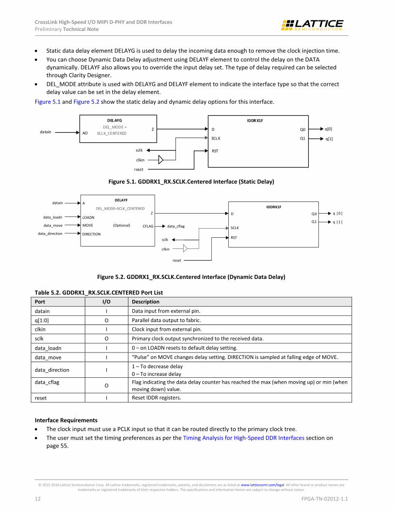
5.2.1. GDDRX1_RX.SCLK.Centered
This is a generic receive interface using X1 gearing and SCLK. The input clock is centered relative to the data. This interface can be used for DDR data rates below 400 Mb/s.
This DDR interface uses the following modules:
IDDRX1F element to capture the data.
The incoming clock is routed through the Primary (SCLK) clock tree.
CrossLink High-Speed I/O MIPI D-PHY and DDR Interfaces Preliminary Technical Note
© 2015-2016 Lattice Semiconductor Corp. All Lattice trademarks, registered trademarks, patents, and disclaimers are as listed at www.latticesemi.com/legal. All other brand or product names are trademarks or registered trademarks of their respective holders. The specifications and information herein are subject to change without notice.
12 FPGA-TN-02012-1.1
Static data delay element DELAYG is used to delay the incoming data enough to remove the clock injection time.
You can choose Dynamic Data Delay adjustment using DELAYF element to control the delay on the DATA dynamically. DELAYF also allows you to override the input delay set. The type of delay required can be selected through Clarity Designer.
DEL_MODE attribute is used with DELAYG and DELAYF element to indicate the interface type so that the correct delay value can be set in the delay element.
Figure 5.1 and Figure 5.2 show the static delay and dynamic delay options for this interface.
Figure 5.1. GDDRX1_RX.SCLK.Centered Interface (Static Delay)
IDDRX1F
SCLK
D Q0
Q1
RST
datain
reset
q [0 ]
q [1 ]
ADELAYF
LOADN
MOVE
DIRECTION
Zdata_loadn
data_move
data_direction
clkin
(Optional)
DEL_MODE=SCLK_CENTERED
CFLAG
sclk
data_cflag
Figure 5.2. GDDRX1_RX.SCLK.Centered Interface (Dynamic Data Delay)
Table 5.2. GDDRX1_RX.SCLK.CENTERED Port List
Port I/O Description
datain I Data input from external pin.
q[1:0] O Parallel data output to fabric.
clkin I Clock input from external pin.
sclk O Primary clock output synchronized to the received data.
data_loadn I 0 – on LOADN resets to default delay setting.
data_move I “Pulse” on MOVE changes delay setting. DIRECTION is sampled at falling edge of MOVE.
data_direction I 1 – To decrease delay
0 – To increase delay
data_cflag O
Flag indicating the data delay counter has reached the max (when moving up) or min (when moving down) value.
reset I Reset IDDR registers.
Interface Requirements
The clock input must use a PCLK input so that it can be routed directly to the primary clock tree.
The user must set the timing preferences as per the Timing Analysis for High-Speed DDR Interfaces section on page 55.
CrossLink High-Speed I/O MIPI D-PHY and DDR Interfaces Preliminary Technical Note
© 2015-2016 Lattice Semiconductor Corp. All Lattice trademarks, registered trademarks, patents, and disclaimers are as listed at www.latticesemi.com/legal. All other brand or product names are trademarks or registered trademarks of their respective holders. The specifications and information herein are subject to change without notice.
FPGA-TN-02012-1.1 13
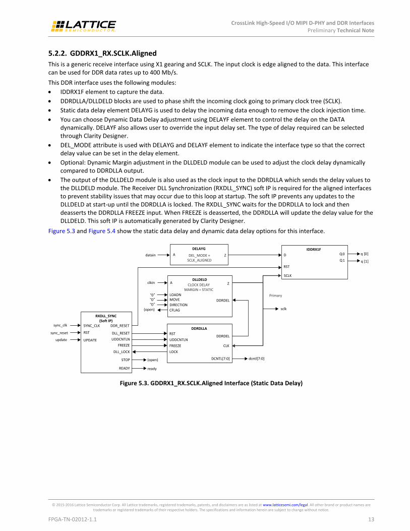
5.2.2. GDDRX1_RX.SCLK.Aligned
This is a generic receive interface using X1 gearing and SCLK. The input clock is edge aligned to the data. This interface can be used for DDR data rates up to 400 Mb/s.
This DDR interface uses the following modules:
IDDRX1F element to capture the data.
DDRDLLA/DLLDELD blocks are used to phase shift the incoming clock going to primary clock tree (SCLK).
Static data delay element DELAYG is used to delay the incoming data enough to remove the clock injection time.
You can choose Dynamic Data Delay adjustment using DELAYF element to control the delay on the DATA dynamically. DELAYF also allows user to override the input delay set. The type of delay required can be selected through Clarity Designer.
DEL_MODE attribute is used with DELAYG and DELAYF element to indicate the interface type so that the correct delay value can be set in the delay element.
Optional: Dynamic Margin adjustment in the DLLDELD module can be used to adjust the clock delay dynamically compared to DDRDLLA output.
The output of the DLLDELD module is also used as the clock input to the DDRDLLA which sends the delay values to the DLLDELD module. The Receiver DLL Synchronization (RXDLL_SYNC) soft IP is required for the aligned interfaces to prevent stability issues that may occur due to this loop at startup. The soft IP prevents any updates to the DLLDELD at start-up until the DDRDLLA is locked. The RXDLL_SYNC waits for the DDRDLLA to lock and then deasserts the DDRDLLA FREEZE input. When FREEZE is deasserted, the DDRDLLA will update the delay value for the DLLDELD. This soft IP is automatically generated by Clarity Designer.
Figure 5.3 and Figure 5.4 show the static data delay and dynamic data delay options for this interface.
IDDRX1F
SCLK
D Q0
Q1
RST
datain q [0]
q [1]
clkin
A
DELAYG
Z
DLLDELDZA
DDRDEL
LOADN
DIRECTION
CFLAG
“0”“0”
(open)
Primary
DEL_MODE =SCLK_ALIGNED
UPDATE
sync_reset
READY
“0”MOVE
DDRDLLA
DDRDEL
CLK
DCNTL[7:0]
RST
UDDCNTLN
FREEZE
LOCK
(open)
ready
RXDLL_SYNC (Soft IP)
SYNC_CLK
RST
sync_clk
update
DDR_RESET
DLL_RESET
UDDCNTLN
FREEZE
DLL_LOCK
STOP dcntl[7:0]
CLOCK DELAY MARGIN = STATIC
sclk
Figure 5.3. GDDRX1_RX.SCLK.Aligned Interface (Static Data Delay)

CrossLink High-Speed I/O MIPI D-PHY and DDR Interfaces Preliminary Technical Note
© 2015-2016 Lattice Semiconductor Corp. All Lattice trademarks, registered trademarks, patents, and disclaimers are as listed at www.latticesemi.com/legal. All other brand or product names are trademarks or registered trademarks of their respective holders. The specifications and information herein are subject to change without notice.
14 FPGA-TN-02012-1.1
data_loadn
data_move
data_direction
A
DELAYF
LOADN
MOVE
DIRECTION
CFLAG
datain
q[0]
q[1]
clkinDLLDELD
ZA
DDRDELLOADN
MOVE
DIRECTION
CFLAG
IDDRX1F
SCLK
DQ0
Q1
RST
CLK
RST
UDDCNTLN
FREEZE
DDRDEL
LOCK
DDRDLLA
DCNTL[7:0] dcntl[7:0]
clock_loadn
clock_move
clock_direction
clock_cflag
data_cflag
7
Z
Primary
(optional)
DEL_MODE=SCLK_ALIGNED
STOP
DLL_LOCK
FREEZEUDDCNTLNDDL_RESET
DDR_RESETSYNC_CLK
RST
UPDATE
sync _ clk
sync_reset
update
READY
(open)
RX_DLLSYNC (Soft IP)
ready
sclk
Figure 5.4. GDDRX1_RX.SCLK.Aligned Interface (Dynamic Data/Clock Delay)
Table 5.3. GDDRX1_RX.SCLK.ALIGNED Port List
Port I/O Description
datain I Data input from external pin.
q[1:0] O Parallel data output to fabric.
clkin I Clock input from external pin.
sclk O Primary clock output synchronized to the received data.
sync_clk I Startup clock. This cannot be the refclk or divided version. It can be other low speed continuously running clock. For example, oscillator clock.
sync_reset I Active high reset to this sync circuit. When RST is asserted to High, then STOP and READY go low while DDR_RESET goes to High.
ready O RXDLL sync is achieved, data is ready to receive
update I Start the RXDLL sync procedure, or restart if need to optimize again.
dcntl [7:0] O The delay codes from the DDRDLL available for the user IP.
data_loadn I 0 – On LOADN resets to default delay setting
data_move I “Pulse” on MOVE changes delay setting. DIRECTION is sampled at falling edge of MOVE.
data_direction I 1 – To decrease delay
0 – To increase delay
data_cflag O
Flag indicating the data delay counter has reached the max (when moving up) or min (when moving down) value.
clock_loadn I Used to reset back to 90° delay from the DDRDLLA code.
clock_move I Pulse is required to change delay settings. The value on Direction is sampled at the falling edge of MOVE.
clock_direction I Indicates delay direction.
1 – To decrease delay
0 – To increase delay
clock_cflag O Indicates the delay counter has reached its maximum value when moving up or minimum value when moving down.
Interface Requirements
The clock input must use a PCLK input so that it can be routed directly to the DLLDELD input.
The user must set the timing preferences as per the Timing Analysis for High-Speed DDR Interfaces section on page 55.

CrossLink High-Speed I/O MIPI D-PHY and DDR Interfaces Preliminary Technical Note
© 2015-2016 Lattice Semiconductor Corp. All Lattice trademarks, registered trademarks, patents, and disclaimers are as listed at www.latticesemi.com/legal. All other brand or product names are trademarks or registered trademarks of their respective holders. The specifications and information herein are subject to change without notice.
FPGA-TN-02012-1.1 15
5.2.3. GDDRX2_RX.ECLK.Centered (1:4 Gearing), GDDRX4_RX.ECLK.Centered (1:8 Gearing) and GDDRX8_RX.ECLK.Centered (1:16 Gearing)
These are Generic receive interfaces using X2, X4, or X4 gearing and Edge Clock Tree (ECLK). The input clock is centered relative to the data. These interfaces must be used for DDR data rates above 400 Mb/s as shown in Table 4.1 on page 9.
This DDR interface uses the following modules:
IDDRX2F element for X2 mode (1:4 gearing)
IDDRX4C element for X4 mode (1:8 gearing)
IDDRX8A element for X4 mode (1:16 gearing)
The incoming clock is routed to the Edge clock (ECLK) clock tree through the ECLKSYNCB module.
CLKDIVG module is used to divide the incoming clock by 2 for X2 gearing, by 4 for X4 gearing and by 8 for x8 gearing. For details on CLKDIVG, refer to FPGA-TN-02015, CrossLink sysCLOCK PLL/DLL Design and Usage Guide.
Static data delay element DELAYG to delay the incoming data enough to remove the clock injection time.
At initialization either the GDDR_SYNC soft IP can be used to make sure the modules are in sync or the RESET of the DDR modules can be connected to the STOP port of the ECLKSYNC module.
By default the RESET is connected to the STOP of the ECLKSYNC module, the user can enable the GDDR_SYNC soft IP through the GUI if needed.
Optional the Dynamic Data Delay adjustment using DELAYF can be enabled using the GUI as well.
These dynamic options give the user better control over the data margin window.
Figure 5.5, Figure 5.6, and Figure 5.7 show the static delay and dynamic delay options for this interface.
ALIGNWD
datain
clkin
A
DELAYG Z
ECLKI
STOPECLKO
SCLK
D
RSTALIGNWD
ECLK
IDDRX2F
Edge
Primarysclk
CLKDIVG
CLKI
RSTCDIVX
alignWD
q [3:0]
ECLKSYNCB
DEL_MODE=ECLK_CENTERED
reset
Q [3:0]
Figure 5.5. GDDRX2_RX.ECLK.Centered Interface (Static Delay)
A
DELAYG
datain Z
ECLKI
STOPECLKO
SCLK
D
RSTALIGNWD
ECLK
Edge
Primarysclk
CLKDIVG
CLKI
RST
CDIVX
alignwd
clkin
Q[3:0] q [3:0]
IDDRX2F
ECLKSYNCB
sync_reset
GDDR_SYNC
sync_clk
start
RST
START
SYNC_CLK
DDR_RESET
STOP
READY ready
DEL_MODE=ECLK_CENTERED
Figure 5.6. GDDRX2_RX.ECLK.Centered Interface (Static Delay) with GDDR_SYNC Soft IP

CrossLink High-Speed I/O MIPI D-PHY and DDR Interfaces Preliminary Technical Note
© 2015-2016 Lattice Semiconductor Corp. All Lattice trademarks, registered trademarks, patents, and disclaimers are as listed at www.latticesemi.com/legal. All other brand or product names are trademarks or registered trademarks of their respective holders. The specifications and information herein are subject to change without notice.
16 FPGA-TN-02012-1.1
Figure 5.7. GDDRX2_RX.ECLK.Centered Interface (Dynamic Data Delay) without GDDR_SYNC Soft IP
Note: Figure 5.7 shows the X2 gearing interface. The X4 and X8 gearing interfaces are similar but use the IDDRX4C and IDDRX8A primitives.
Table 5.4. GDDRX2_RX.ECLK.CENTERED Port List
Port I/O Description
datain I Data input from external pin.
q[3:0] O Parallel data output to fabric.
clkin I Clock input from external pin.
sclk O Primary clock output synchronized to the received data.
data_loadn I 0 – On LOADN resets to default delay setting.
data_move I “Pulse” on MOVE changes delay setting. DIRECTION is sampled at falling edge of MOVE.
data_direction I 1 – To decrease delay
0 – To increase delay
data_cflag O
Flag indicating the data delay counter has reached the max (when moving up) or min (when moving down) value.
reset I Reset IDDR registers.
alignwd I This signal is used for word alignment. It shifts the word by 1 bit.
Interface Requirements
The ECLKSYNCB “STOP” input should be tied to the RESET of CLKDIVG and IDDR modules if not using the GDDR_SYNC soft IP. For details on ECLKSYNCB module, refer to FPGA-TN-02015, CrossLink sysCLOCK PLL/DLL Design and Usage Guide.
The clock input must use a PCLK input so that it can be routed directly to the edge clock tree.
DELAYF is used when user selects Dynamic Data Delay.
The user must set the timing preferences as per the Timing Analysis for High-Speed DDR Interfaces section on page 55.
5.2.4. GDDRX2_RX.ECLK.Aligned (1:4 Gearing), GDDRX4_RX.ECLK.Aligned (1:8 Gearing) and GDDRX8_RX.ECLK.Aligned (1:16 Gearing)
These are generic receive interfaces using X2, X4, or X4 gearing and Edge Clock Tree (ECLK). The input clock is edge aligned to the data. These interfaces must be used for DDR data rates above 400 Mb/s as shown in Table 4.1 on page 9. This DDR interface uses the following modules:
IDDRX2F element for X2 mode
IDDRX4C element for X4 mode

CrossLink High-Speed I/O MIPI D-PHY and DDR Interfaces Preliminary Technical Note
© 2015-2016 Lattice Semiconductor Corp. All Lattice trademarks, registered trademarks, patents, and disclaimers are as listed at www.latticesemi.com/legal. All other brand or product names are trademarks or registered trademarks of their respective holders. The specifications and information herein are subject to change without notice.
FPGA-TN-02012-1.1 17
IDDRX8A element for X4 mode
DDRDLLA/DLLDELD blocks to phase shift the incoming clock routed to the Edge clock (ECLK) clock tree through the ECLKSYNCB module.
CLKDIVG module is used to divide the incoming clock by 2 for X2 gearing, by 4 for x4 gearing and by 8 for x8 gearing.
Static data delay element DELAYG to delay the incoming data enough to remove the clock injection time.
Unlike the Centered interface for Aligned interface it is required to use the RXDLL_SYNC module.
Optional the Dynamic Data delay adjustment using DELAYF can be enable using the GUI as well.
These dynamic options give the user better control over the data margin window.
datain
clkin
A
DELAYG Z
DLLDELDZA
DDRDEL
LOADN
MOVE
DIRECTIONCFLAG
CLK
RST
UDDCNTLN
FREEZE
DDRDEL
LOCK
DDRDLLA
DCNTL[7:0]
“0”“0”
(open)
ECLKI
STOPECLKO
SCLK
D
RSTALIGNWD
ECLK
Edge
Primary
CLKDIVGCLKI
RST
ALIGNWD
CDIVX
alignwd
IDDRX2F
Q [3:0] q[3:0]
ECLKSYNCB
dcntl[7:0]
STOP
DLL_LOCK
FREEZE
UDDCNTLN
DLL_RESET
DDR_RESETSYNC_CLK
RST
UPDATE
sync_clk
sync_reset
update
READY ready
RXDLL_SYNC (Soft IP)
DEL_MODE=ECLK_CENTERED
sclk
“0”
Figure 5.8. GDDRX2_RX.ECLK.Aligned Interface (Static Delay) with RXDLL_SYNC IP
d ata_loadn
d ata_move
d ata_d irection
ADELAYF
LOADN
MOVE
DIR E C TION
C F LAG
d atain
c lkinDLLDELD
ZA
DDR DE L
LOADN
MOVE
DIR E C TION
C F LAG
C LK
R S T
UDDC NTLN
F R E E ZE
DDR DE L
LOC K
DDRDLLA
DCNTL[7:0] d cntl[7:0]
c lock_loadn
c lock_move
c lock_d irection
c lock_c f lag
d ata_c f lag
Z
E C LK I
S TOP
E C LK O
S C LK
D
R S T
ALIGNWD
E C LK
E dge
P rimarysclk
CLKDIVG
C LK I
R S T
AL IGNWD
C DIVX
a lignw d
Q[3:0] q [3:0]
IDDRX2F
ECLKSYNCB
(optional)
S TOP
DLL_LOC K
F R E E ZE
UDDC NTLN
DLL_R E S E T
DDR _R E S E TS Y NC _C LK
R S T
UP DATE
s ync_clk
s ync_reset
u pdate
R E ADY
RXDLL_SYNC (Soft IP)
ready
DEL_MODE=ECLK_CENTERED
Figure 5.9. GDDRX2_RX.ECLK.Aligned Interface (Dynamic Data/Clock Delay)
Note: Figure 5.9 shows the X2 gearing interface. The X4 and X8 gearing interfaces are similar but use the IDDRX4C and IDDRX8A primitives.

CrossLink High-Speed I/O MIPI D-PHY and DDR Interfaces Preliminary Technical Note
© 2015-2016 Lattice Semiconductor Corp. All Lattice trademarks, registered trademarks, patents, and disclaimers are as listed at www.latticesemi.com/legal. All other brand or product names are trademarks or registered trademarks of their respective holders. The specifications and information herein are subject to change without notice.
18 FPGA-TN-02012-1.1
Table 5.5. GDDRX2_RX.ECLK.ALIGNED Port List
Port I/O Description
datain I Data input from external pin.
q[3:0] O Parallel data output to fabric.
clkin I Clock input from external pin.
sclk O Primary clock output synchronized to the received data.
sync_clk I Startup clock. This cannot be the refclk or divided version. It can be other low speed continuously running clock. For example, oscillator clock.
sync_reset I Active high reset to this sync circuit. When RST is asserted to High, then STOP and READY go low while DDR_RESET goes to High.
ready O RXDLL sync is achieved, data is ready to receive.
update I Start the RXDLL sync procedure, or restart if need to optimize again.
dcntl [7:0] O The delay codes from the DDRDLL available for the user IP.
data_loadn I 0 – On LOADN resets to default delay setting.
data_move I “Pulse” on MOVE changes delay setting. DIRECTION is sampled at falling edge of MOVE.
data_direction I 1 – To decrease delay
0 – To increase delay
data_cflag O
Flag indicating the data delay counter has reached the max (when moving up) or min (when moving down) value.
clock_loadn I Used to reset back to 90° delay from the DDRDLLA code.
clock_move I Pulse is required to change delay settings. The value on Direction is sampled at the falling edge of MOVE.
clock_direction I Indicates delay direction.
1 – To decrease delay
0 – To increase delay
clock_cflag O Indicates the delay counter has reached its maximum value when moving up or minimum value when moving down.
Interface Requirements
The clock input must use a PCLK input so that it can be routed directly to the edge clock tree.
When Enable dynamic Margin Control option is selected the dynamic inputs of the DLLDELD should be brought out to ports.
DELAYF is used when user selects Dynamic Data Delay.
RXDLL_SYNC module must be instantiated as a part of this interface. Clarity Designer automatically adds it when this interface is selected.
The user must set the timing preferences as per the Timing Analysis for High-Speed DDR Interfaces section on page 55.
5.3. 7:1 LVDS Receive Interfaces
5.3.1. GDDRX71_RX.ECLK (1:7 Gearing) and GDDRX141_RX.ECLK (1:14 Gearing)
This is a specialized receive interface (called 7:1 LVDS, FPD-Link, or OpenLDI) using 1:7 gearing (or 1:14) and ECLK. The input clock coming in is multiplied 3.5X using a PLL. The multiplied clock is used to capture the data at the receive IDDRX module.
This DDR interface uses the following modules:
IDDRX71B element is used to capture the data. (Alternatively IDDRX141A can be used for higher data rates).
EHXPLLM multiplies the input clock by 3.5 and phase shifts the incoming clock based on the dynamic phase shift input.
This clock is routed to the edge clock tree (ECLK) through the ECLKSYNCB module.

CrossLink High-Speed I/O MIPI D-PHY and DDR Interfaces Preliminary Technical Note
© 2015-2016 Lattice Semiconductor Corp. All Lattice trademarks, registered trademarks, patents, and disclaimers are as listed at www.latticesemi.com/legal. All other brand or product names are trademarks or registered trademarks of their respective holders. The specifications and information herein are subject to change without notice.
FPGA-TN-02012-1.1 19
CLKDIVG module is used to divide the ECLK by 3.5 for 1:7 Gearing or by 7 for 1:14 Gearing and route the SCLK to the primary clock tree.
A second IDDR71B or IDDR141A element is used with clock connected to the data input to generate 7-bit (or 14-bit) clock phase.
The GDDR_SYNC soft IP must be used for startup sync.
The BW_ALIGN soft IP may be included for bit and word alignment.
DELAYF modules can be added to enable tuning the receiver timing between clock and data.
datain
clkin
EXHPLLMCLKOP
CLKI
PHASESEL
PHASEDIR
RST
CLKFB
CLKOS
LOC KPHASESTEP
pl l_reset
sync_reset
PHASELOADREG
phasedir
“0”
phasestep
phaseloadreg
Figure 5.10. GDDRX71_RX.ECLK Interface (DELAYF and BW_ALIGN not enabled)

CrossLink High-Speed I/O MIPI D-PHY and DDR Interfaces Preliminary Technical Note
© 2015-2016 Lattice Semiconductor Corp. All Lattice trademarks, registered trademarks, patents, and disclaimers are as listed at www.latticesemi.com/legal. All other brand or product names are trademarks or registered trademarks of their respective holders. The specifications and information herein are subject to change without notice.
20 FPGA-TN-02012-1.1
datain
clkin
EXHPLLMCLKOP
CLKI
PHASEDIR
RST
CLKFB
CLKOS
LOCKPHASESTEP
pll_reset
sync_reset
PHASELOADREG
Figure 5.11. GDDRX71_RX.ECLK Interface with GDDR_SYNC and BW_ALIGN Soft IP
datain
clkin
EXHPLLMCLKOP
CLKI
PHASESEL
PHASEDIR
RST
CLKFB
CLKOS
LOCKPHASESTEP
pll_reset
sync_reset
PHASELOADREG
A
DELAYF
DIRECTION
Z
CFLAG
MOVELOADN
A
DELAYF
DIRECTION
Z
CFLAG
MOVELOADN
data_cflag
clock_cflag
Figure 5.12. GDDRX71_RX.ECLK Interface with GDDR_SYNC, BW_ALIGN Soft IP and DELAYF Tuning

CrossLink High-Speed I/O MIPI D-PHY and DDR Interfaces Preliminary Technical Note
© 2015-2016 Lattice Semiconductor Corp. All Lattice trademarks, registered trademarks, patents, and disclaimers are as listed at www.latticesemi.com/legal. All other brand or product names are trademarks or registered trademarks of their respective holders. The specifications and information herein are subject to change without notice.
FPGA-TN-02012-1.1 21
datain
clkin
EHXPLLMCLKOP
CLKI
PHASESEL
PHASEDIR
RSTECLKI
STOP
ECLKO
Edge
Primary
sclk
CLKDIVG
CLKI
RST
ALIGNWD
CDIVX
CLKFB
CLKOS
LOCKPHASESTEP
SCLK
DQ 0
Q 1
RST
ALIGNWD
ECLK
SCLK
D Q 0Q 1
RST
ALIGNWD
ECLK
q [0]
q [1]
ECLKSYNCB
pll_reset
sync_resetGDDR_SYNC
sync_clkRST
START
SYNC_CLK
DDR_RESET
STOP
READY ready
RX _ SCLK
RXCLK _WORD < 6:0>UPDATE
SYNC_READY
RST
PHASESTEP
PHASEDIR
ALIGNWORD
WINDOW_SIZE
BIT_ LOCK
WORD _LOCK
READY align_ready
update
bw _ align _ rstwindow_size[3:0]
bit_lock
word_lock
PHASELOADREG“1”
DELAY_LOADNDELAY_MOVEDELAY_DIRECTION
ADELAYF
DIRECTION
Z
CFLAG
MOVELOADN
A
DELAYF
DIRECTION
ZCFLAG
MOVELOADN
BW_ALIGN
(divby7)
IDDR141A
... ...
...
IDDR141A
Q12
Q13
Q12Q13
q
q
clock_phase [13:0]
clock_cflag
data_cflag
Figure 5.13. GDDRX141_RX.ECLK Interface with GDDR_SYNC, BW_ALIGN and DELAYF Tuning Soft IP
Note: BW_ALIGN and DELAYF tuning are optional in the GDDRX141 interface. Implementations without these modules will be connected similar to the connections in Figure 5.10 and Figure 5.11.
Table 5.6. GDDRX71_RX.ECLK Port List
Port I/O Description
datain I Data input from external pin.
q[6:0] O Parallel data output to fabric.
clkin I Clock input from external pin.
sclk O Primary clock output synchronized to the received data.
pll_reset I Reset PLL, will cause other modules to reset as well.
sync_clk I Startup clock. This cannot be the refclk or divided version. It can be other low speed
continuously running clock. For example, oscillator clock.
sync_reset I Active high reset to this sync circuit. When RST is asserted to High, then STOP and READY
go low while DDR_RESET goes to High.
clock_phase[6:0] O 7-bits of clock phase, used by byte / word aligner.
update I Start the byte/word align procedure, or restart if need to optimize again.
window[3:0] O Final valid window size.
bit_lock O Status output, bit lock has been achieved.
word_lock O Status output, word lock has been achieved.
align_ready O Indicate that alignment procedure is finished and Rx circuit is ready to operate.
data_cflag O Flag indicating the data delay counter has reached the max (when moving up) or min (when moving down) value.
clock_cflag O Flag indicating the data delay counter has reached the max (when moving up) or min (when moving down) value.
bit_align_rst I Reset bit align module.

CrossLink High-Speed I/O MIPI D-PHY and DDR Interfaces Preliminary Technical Note
© 2015-2016 Lattice Semiconductor Corp. All Lattice trademarks, registered trademarks, patents, and disclaimers are as listed at www.latticesemi.com/legal. All other brand or product names are trademarks or registered trademarks of their respective holders. The specifications and information herein are subject to change without notice.
22 FPGA-TN-02012-1.1
Interface Requirements
START of GDDR_SYNC should be connected to PLL Lock output.
The SYNC_CLK should be sourced by the oscillator clock or other constant running low speed clock. Note that this clock should not come from clock sources that this module stops or resets (such as ECLKSYNC, CLKDIV)
The clock input must use a dedicated PLL input pin routed directly to the PLL.
The CLKOP of the PLL is routed to a separate edge clock back to the PLL CLKFB to remove the clock path delay across the operating range of the device.
BW_ALIGN soft IP may be enabled to determine the right phase of the input clock and to drives the dynamic phase adjustments of the PLL. It also drives the ALIGNWD input of the CLKDIVG and IDDRX71B to achieve a 7-bit word alignment.
GDDR_SYNC soft IP is required to tolerate the large skew between stop and reset.
5.4. MIPI D-PHY Receive Interfaces The CrossLink device family provides two distinct hardware solutions for D-PHY receive. The programmable LVDS banks (Bank 1 and Bank 2) support a soft D-PHY receive function using a combination of the MIPI I/O buffers, Input DDR elements and clock and delay elements. CrossLink also includes up to two hardened D-PHY blocks, which support both Rx and Tx.
5.4.1. MIPI DSI Receive Interface – Soft D-PHY Module
The Input DDR elements can be configured as MIPI-D-PHY inputs to receive MIPI DSI data using the X4 and X8 gearing with ECLK sync and clock divider elements. MIPI D-PHY uses a center-aligned clock. The interfaces use the programmable LVDS I/O as input MIPI buffers. For DSI the D0 bit supports BIDI capability for the LP mode.
This DDR interface uses the following modules:
MIPI I/O buffer used to receive the MIPI data and clock. Refer to FPGA-TN-02016, CrossLink sysI/O Usage Guide for more details on the MIPI I/O buffer.
The HSSEL input of the MIPI buffer is used to switch between the High-Speed and Low-Power modes. The transitions between High-Speed (HS) and Low-Power (LP)
The RXHSEN and TXLPEN inputs are connected to the TP/TN tristate control inputs of the MIPI I/O buffer to control the LP ports which can be bidirectional.
When in High-Speed mode:
Differential data received at the BP/BN ports (either DPx/DNx or CLKP/CLKN) is output on the OHS port
The OHS of the data MIPI element is connected to the Data input of the IDDRX4C or IDDRX8A element via the DELAYG element in centered mode. The output of the IDDRX4C or IDDRX8A element is connected to the fabric as HSRXDATA[7:0] (x4 gearing) or HSRXDATA[15:0] (x8 gearing).
The OHS of the clock MIPI is connected through the ECLKSYNCB element to the data input DDR elements as well as the CLKDIVG element (both ECLKSYNCB and CLKDIVG are described in detail in FPGA-TN-02015, CrossLink sysCLOCK PLL/DLL Design and Usage Guide). The CLKDIVG generates the RXBYTECLK signal which is connected to the fabric. HSRXDATA signals are synchronized to the RXBYTECLK.
When in Low-Power mode:
The OLSP and OLSN outputs of MIPI are active and transmitting data on the RXLPP and RXLPN ports to the fabric as shown in Figure 5.14. The OLSP and OLSN can also be inputs, it depends on the state of RXHSEN and TXLPEN which control TP/TN tristate inputs. The OLSP and OLSN states are also used to generate the D0_CD or CLK_CD signals which can be monitored by the fabric for contention detection.

CrossLink High-Speed I/O MIPI D-PHY and DDR Interfaces Preliminary Technical Note
© 2015-2016 Lattice Semiconductor Corp. All Lattice trademarks, registered trademarks, patents, and disclaimers are as listed at www.latticesemi.com/legal. All other brand or product names are trademarks or registered trademarks of their respective holders. The specifications and information herein are subject to change without notice.
FPGA-TN-02012-1.1 23
DP0
DN0
D0_TXLPEN
BPBN
HSSEL
OHS
OLSP
CLKP
CLKN
IPIN
D0_TXLPP
TP
TNOLSN
MIPI
D0_RXHSEN
D0_TXLPN
D0_RXLPP
D0_RXLPN
OR D0_CD
CLK_RXHSEN
1'b1CLK_RXLPP
CLK_RXLPN
OR CLK_CD
DxP
DxN
ECLKI
STOP ECLKO
ECLKSYNCBReset
SCLK
D Q[15:0]
RSTALIGNWD
ECLK
IDDRX8ADx_HSRXDATA[15:0]
RXBYTECLK
*x = 1, 2, 3
AND
ADELAYG
Z
SCLK
D Q[15:0]
RST
ALIGNWD
ECLK
IDDRX8A
DEL_MODE=ECLK_CENTERED
D0_HSRXDATA[15:0]
ALIGNWD
PrimaryCLKDIVGCLKI
RST CDIVXBPBN
HSSELOHS
OLSP
IPINTP
TNOLSN
MIPI
BPBN
HSSEL
OHS
OLSP
IPINTP
TNOLSN
MIPI
1'b1
1'b1
1'b1
ADELAYG
ZDEL_MODE=
ECLK_CENTERED
1'b0
1'b0
1'b0
Figure 5.14. MIPI DSI Receive Interface with Soft D-PHY Module
Note: Figure 5.14 shows the X8 gearing interface. X4 is similar but uses the IDDRX4C primitive.
Table 5.7. MIPI DSI Receive Interface with Soft D-PHY Port List
Pin Name I/O Description
CKP I MIPI Input Positive Clock
CKN I MIPI Input Negative Clock
RXBYTECLK O Byte Clock Output – Geared down clock from the CLK Input
CLK_RXHSEN I High-Speed Clock Receiver Enable Signal
CLK_RXLPP O Low Power Clock Receiver Positive Data Output
CLK_RXLPN O Low Power Clock Receiver Negative Data Output
CLK_CD O Low Power Clock Contention Detector Output
D0_TXLPP I Low Power Data Transmitter Positive Data Input
D0_TXLPEN I Low Power Data Transmitter Enable Signal
D0_TXLPN I Low Power Data Transmitter Negative Data Input
DP0 I/O MIPI I/O Positive Data Lane 0
DN0 I/O MIPI I/O Negative Data Lane 0
DxN I MIPI Input Data
DxP I MIPI Input Data
D0_RXLPP O Low Power Data Receiver Positive Data Output
D0_RXLPN O Low Power Data Receiver Negative Data Output
D0_CD O Low Power Data Contention Detector Output
D0_RXHSEN I High-Speed Data Receiver Enable Signal
DyHSRXDATA[15:0] O Eight Bit High-Speed data received. DY_HSRX_DATA[0] is received first.
reset I Asynchronous reset to the interface.

CrossLink High-Speed I/O MIPI D-PHY and DDR Interfaces Preliminary Technical Note
© 2015-2016 Lattice Semiconductor Corp. All Lattice trademarks, registered trademarks, patents, and disclaimers are as listed at www.latticesemi.com/legal. All other brand or product names are trademarks or registered trademarks of their respective holders. The specifications and information herein are subject to change without notice.
24 FPGA-TN-02012-1.1
Interface Requirements
The clock input must use a PCLK input so that it can be routed directly to the edge clock tree.
GDDRX_SYNC soft IP is optional for startup synchronization. By default the STOP input of ECLKSYNC is connect to the RESET.
Bank 1 and Bank 2 of LIF-MD6000 support the Soft D-PHY.
Assigned I/O will be configured as the MIPI I/O type.
5.4.2. MIPI CSI2 Receive Interface – Soft D-PHY Module
The Input DDR elements can be configured as MIPI-D-PHY inputs to receive MIPI DSI data using the X4 and X8 gearing with ECLK sync and clock divider elements. MIPI D-PHY uses a center-aligned clock. The interfaces use the programmable LVDS I/O as input MIPI buffers. The only difference between the DSI and CSI-2 D-PHY interfaces is the LP ports for CSI-2 are not bidirectional, they are only receive.
This DDR interface uses the following modules:
MIPI I/O buffer used to receive the MIPI data and clock (Refer to FPGA-TN-02016, CrossLink sysI/O Usage Guide for more details on the MIPI I/O buffer).
The RXHSEN inputs to the interface block are tied to the HSSEL input of the MIPI buffer to switch between the High-Speed and Low-Power modes. The transitions between High-Speed (HS) and Low-Power (LP).
The TP/TN is the tristate port used to switch LP ports which can be bidirectional. But in this mode, the LP ports are always receive, so the TP/TN ports are internally tied off to always receive.
When in High-Speed mode:
Differential data received at the BP/BN ports (either DPx/DNx or CLKP/CLKN) is output on the OHS port
The OHS of the data MIPI element is connected to the Data input of the IDDRX4C or IDDRX8A element via the DELAYG element in centered mode. The output of the IDDRX4C or IDDRX8A element is connected to the fabric as HSRXDATA[7:0] (x4 gearing) or HSRXDATA[15:0] (x8 gearing).
The OHS of the clock MIPI is connected through the ECLKSYNCB element to the data input DDR elements as well as the CLKDIVG element (both ECLKSYNCB and CLKDIVG are described in detail in FPGA-TN-02015, CrossLink sysCLOCK PLL/DLL Design and Usage Guide). The CLKDIVG generates the RXBYTECLK signal which is connected to the fabric. HSRXDATA signals are synchronized to the RXBYTECLK.
When in Low-Power mode:
The OLSP and OLSN outputs of MIPI are active and transmitting data on the RXLPP and RXLPN ports to the fabric as shown in Figure 5.15. The OLSP and OLSN states are also used to generate the D0_CD or CLK_CD signals which can be monitored by the fabric for contention detection.

CrossLink High-Speed I/O MIPI D-PHY and DDR Interfaces Preliminary Technical Note
© 2015-2016 Lattice Semiconductor Corp. All Lattice trademarks, registered trademarks, patents, and disclaimers are as listed at www.latticesemi.com/legal. All other brand or product names are trademarks or registered trademarks of their respective holders. The specifications and information herein are subject to change without notice.
FPGA-TN-02012-1.1 25
DP0
DN0BPBN
HSSEL
OHS
OLSP
CLKP
CLKN
IPINTP
TNOLSN
MIPI
D0_RXHSEN
D0_RXLPP
D0_RXLPN
OR D0_CD
CLK_RXHSEN
1'b1
CLK_RXLPP
CLK_RXLPN
OR CLK_CD
DxP
DxN
ECLKI
STOP ECLKO
ECLKSYNCB
Reset
SCLK
D Q[15:0]
RSTALIGNWD
ECLK
IDDRX8ADx_HSRXDATA[15:0]
RXBYTECLK
*x = 1, 2, 3
ADELAYG
Z
SCLK
D Q[15:0]
RST
ALIGNWD
ECLK
IDDRX8A
DEL_MODE=ECLK_CENTERED
D0_HSRXDATA[15:0]
ALIGNWD
PrimaryCLKDIVGCLKI
RST CDIVXBPBN
HSSEL
OHS
OLSPIPINTP
TNOLSN
MIPI
BPBN
HSSEL
OHS
OLSP
IPINTP
TNOLSN
MIPI
1'b1
1'b1
1'b1
1'b1
ADELAYG
ZDEL_MODE=
ECLK_CENTERED
1'b0
1'b0
1'b0
1'b1
1'b1
Figure 5.15. MIPI CSI-2 Receive Interface with Soft D-PHY Module
Note: Figure 5.15 shows the X8 gearing interface. X4 is similar but uses the IDDRX4C primitive.
Table 5.8. MIPI CSI-2 Receive Interface with Soft D-PHY Port List
Pin Name I/O Description
CKP I MIPI Input Positive Clock
CKN I MIPI Input Negative Clock
RXBYTECLK O Byte Clock Output – Geared down clock from the CLK Input
CLK_RXHSEN I High-Speed Clock Receiver Enable Signal
CLK_RXLPP O Low Power Clock Receiver Positive Data Output
CLK_RXLPN O Low Power Clock Receiver Negative Data Output
CLK_CD O Low Power Clock Contention Detector Output
DPy I/O MIPI Input Positive Data
DNy I/O MIPI Input Negative Data
D0_RXLPP O Low Power Data Receiver Positive Data Output
D0_RXLPN O Low Power Data Receiver Negative Data Output
D0_CD O Low Power Data Contention Detector Output
D0_RXHSEN I High-Speed Data Receiver Enable Signal
DyHSRXDATA[15:0] O Eight Bit High-Speed data received. DY_HSRX_DATA[0] is received first.
reset I Asynchronous reset to the interface.
Interface Requirements
The clock input must use a PCLK input so that it can be routed directly to the edge clock tree.
GDDRX_SYNC soft IP is optional for startup synchronization. By default the STOP input of ECLKSYNC is connected to the RESET.
Bank 1 and Bank 2 of LIF-MD6000 support the Soft D-PHY.
Assigned I/O will be configured as the MIPI I/O type.

CrossLink High-Speed I/O MIPI D-PHY and DDR Interfaces Preliminary Technical Note
© 2015-2016 Lattice Semiconductor Corp. All Lattice trademarks, registered trademarks, patents, and disclaimers are as listed at www.latticesemi.com/legal. All other brand or product names are trademarks or registered trademarks of their respective holders. The specifications and information herein are subject to change without notice.
26 FPGA-TN-02012-1.1
5.4.3. MIPI DSI Receive Interface – Hard D-PHY Module
The hardened D-PHY blocks can be configured as DSI Receive interfaces.
This hardened D-PHY block is referred to as the MIPIDPHYA primitive in the following discussion. The D-PHY block is automatically configured to receive based on the Clarity Catalog GUI selection.
The MIPIDPHYA primitive is used to receive MIPI data (up to 4 lanes) and clock.
The D0RXHSEN/DxRXHSEN is used to enable high-speed mode.
Figure 5.16 on the next page shows the signals connected to the fabric and the automatic settings when the hardened D-PHY is configured for DSI receive mode. The Clarity Catalog GUI settings automatically powers down unused lanes of the hardened D-PHY.
Only D0 and CLK bits are used in LP mode. Only D0 is used as a bidirectional pin. D1, D2, and D3 pins (when those lanes are used) should be toggled between LP/HS mode based on D0 state as shown in Figure 5.16.
The gearing mode of x8 and x16 are available and the gearing mode is selected by the Clarity Catalog GUI based on the speed of the interface. Depending on the gearing mode, the D-PHY outputs received, de-serialized data on the Dy_HSRXDATA[15:0] (x16 gearing) or Dy_HSRXDATA[7:0] (where y = 1, 2, 3, 4). This data should be connected to the fabric and is synchronized to the RXHSBYTECLK signal.
There are two receive clocks: RXHSBYTECLK and CLKHSBYTE. The receive data is synchronized to the RXHSBYTECLK, but this signal is only active when the de-serializer is running (meaning a properly synchronized HS mode transmission is being received). The CLKHSBYTE is a geared down version of the received clock on the CLKP/CLKN differential pair. This output is always active when the D-PHY is receiving a clock and the CLKRXHSEN is asserted.
The Hard D-PHY includes an integrated PLL block. This is powered down when in DSI receive mode.
The USRSTANDBY port can be used to power down the D-PHY.

CrossLink High-Speed I/O MIPI D-PHY and DDR Interfaces Preliminary Technical Note
© 2015-2016 Lattice Semiconductor Corp. All Lattice trademarks, registered trademarks, patents, and disclaimers are as listed at www.latticesemi.com/legal. All other brand or product names are trademarks or registered trademarks of their respective holders. The specifications and information herein are subject to change without notice.
FPGA-TN-02012-1.1 27
DxRXHSEN (unused lanes)
DyDRXHS
DxHSDESEREN (unused)
DyHSRXDATA[15:0]
HSBYTECLKD
DySYNC
DyERRSYNC
DyNOSYNC
D0DRXLPPD0RXLPEN
D0DRXLPN
D0DCDP
D0CDEN
D0DCDN
CKP
CKN
CLKRXHSENCLKDRXHS
CLKHSBYTE
CLKDRXLPP
CLKDRXLPN
CLKDCDN
CLKRXLPEN
CLKCDEN
DyTXHSEN
DyHSSEREN
DyHSTXDATA[15:0]
HSBYTECLKS
DyTXHSPD
CLKDTXLPP
CLKDTXLPN
CLKTXLPEN
CLKTXHSEN
CLKTXHSGATE
CLKTXHSPD
PDDPHY
LBEN
Bidirectional clk and Data
RX–Data HS Ports
RX–CLK LP Ports
RX–Data LP Ports
DxDTXLPP
DxDTXLPN DxTXLPEN
TX–Data LP Ports
TX–CLK LP Ports
Control Ports
PLL Ports
CLKREF LOCK
MIPIDPHYA
DP0
DN0
PDPLL
PDCKGPDBIAS
DxRXLPEN (unused lanes)
DxCDEN
D0DTXLPP
D0DTXLPN
D0TXLPEN
1'b1
OR
DxDRXLPP
DxDRXLPNDxDCDP
DxDCDN
DPx
DNx
CLKP
CLKN
DPx
DNx
DP0
DN0
D0_RXLPEN
D0_TXLPP
D0_TXLPN
CLK_CD
CLK_RXLPN
CLK_RXLPP
RXHSBYTECLK
Dy_HSRXDATA[15:0]
* x = 1, 2, 3 y = 0, 1, 2, 3
D0_RXLPP
D0_RXHSEN
USRSTDBY
AND
CLK_RXLPEN
CLKRXHSEN
AND
AND
1'b01'b01'b0
1'b0
1'b0
1'b0
1'b1
TX–CLK HS Ports
1'b0
1'b1
1'b0
1'b0
1'b1
TX–Data HS Ports
D0RXHSEN
1'b1
1'b1
D0_RXLPN
D0_CD
1'b1
1'b0
1'b0
RX–CLK HS Ports
DxRXHSEN (used lanes)
DxHSDESEREN (used)
DxRXLPEN (used lanes)
CLKHSBYTE
Figure 5.16. MIPI DSI Receive Interface with Hard D-PHY Module

CrossLink High-Speed I/O MIPI D-PHY and DDR Interfaces Preliminary Technical Note
© 2015-2016 Lattice Semiconductor Corp. All Lattice trademarks, registered trademarks, patents, and disclaimers are as listed at www.latticesemi.com/legal. All other brand or product names are trademarks or registered trademarks of their respective holders. The specifications and information herein are subject to change without notice.
28 FPGA-TN-02012-1.1
Table 5.9. MIPI DSI Hard D-PHY Receive Port List
Pin Name I/O Description
CLKP I/O MIPI Input/Output Positive Clock
CLKN I/O MIPI Input/Output Negative Clock
CLKHSBYTE O Byte Clock Output – Geared down clock from the CLK Input
CLKRXHSEN I High-Speed Clock Receiver Enable Signal
CLK_RXLPP O Low Power Clock Receiver Positive Data Output
CLK_RXLPEN I Low Power Clock Receiver Enable Signal
CLK_RXLPN O Low Power Clock Receiver Negative Data Output
CLK_CD O Low Power Clock Contention Detector Negative Output
DPy I/O MIPI Input/Output Positive Data
DNy I/O MIPI Input/Output Negative Data
D0_RXLPP O Low Power Data Receiver Positive Data Output
D0_RXLPEN I Low Power Data Receiver Enable Signal
D0_RXLPN O Low Power Data Receiver Negative Data Output
D0_CDP O Low Power Data Contention Detector Positive Output
D0_TXLPP I Low Power Data Transmitter Positive Data Input
D0_TXLPN I Low Power Data Transmitter Negative Data Input
D0_RXHSEN I High-Speed Data Receiver Enable Signal
DyHSRXDATA[15:0] O Eight Bit High-Speed data received. DY_HSRX_DATA[0] is received first.
RXHSBYTECLK O High-Speed Receive Byte Clock used to latch the output 8 bits parallel data. This clock is generated from lane D0. DyHSRXDATA is synchronized to this clock.
USRSTDBY I Power Down input for D-PHY. When high, all blocks are powered down.
Note: y=0, 1 ,2, 3
Interface Requirements
The MIPIDPHYA primitive should be mapped to one of the available hardened D-PHY blocks on the CrossLink device. This is done using the LOCATE preference shown below. The component name for the LOCATE preference can be found in the ASIC area of the MAP report in Lattice Diamond. LOCATE COMP " csi2csi_inst/cmos2dphy_inst/dci_wrapper_inst/MIPIDPHYA_inst”
SITE "MIPIDPHY0" ;# constraint for MIPI location
The output of the module RXHSBYTECLK and the CLKHSBYTE should be connected to primary clock tree.
5.4.4. MIPI CSI-2 Receive Interface – Hard D-PHY Module
The hardened D-PHY blocks can be configured as CSI-2 Receive interfaces.
The D-PHY block is automatically configured to receive based on the Clarity Catalog GUI selection.
The MIPIDPHYA primitive is used to receive MIPI data (up to 4 lanes) and clock.
The D0RXHSEN/DxRXHSEN is used to enable high-speed mode.
Figure 5.17 on page 30 shows the signals connected to the fabric and the automatic settings when the hardened D-PHY is configured for CSI-2 receive mode. The Clarity Catalog GUI settings automatically powers down unused lanes of the hardened D-PHY.
Only D0 and CLK bits are used in LP mode. The key difference between CSI-2 and DSI is that the D0 signal is always an input in HS and LP modes, rather than bi-directional. D1, D2, and D3 pins (when those lanes are used) should be toggled between LP/HS mode based on D0 state as shown in Figure 5.17.
The gearing mode of x8 and x16 are available and the gearing mode is selected by the Clarity Catalog GUI based on the speed of the interface. Depending on the gearing mode, the D-PHY outputs received, de-serialized data on the Dy_HSRXDATA[15:0] (x16 gearing) or Dy_HSRXDATA[7:0] (where y = 1, 2, 3, 4). This data should be connected to the fabric and is synchronized to the RXHSBYTECLK signal.
There are two receive clocks: RXHSBYTECLK and CLKHSBYTE. The receive data is synchronized to the RXHSBYTECLK, but this signal is only active when the de-serializer is running (meaning a properly synchronized HS mode

CrossLink High-Speed I/O MIPI D-PHY and DDR Interfaces Preliminary Technical Note
© 2015-2016 Lattice Semiconductor Corp. All Lattice trademarks, registered trademarks, patents, and disclaimers are as listed at www.latticesemi.com/legal. All other brand or product names are trademarks or registered trademarks of their respective holders. The specifications and information herein are subject to change without notice.
FPGA-TN-02012-1.1 29
transmission is being received). The CLKHSBYTE is a geared down version of the received clock on the CLKP/CLKN differential pair. This output is always active when the D-PHY is receiving a clock and the CLKRXHSEN is asserted.
The Hard D-PHY includes an integrated PLL block. This is powered down when in CSI-2 receive mode.
The USRSTANDBY port can be used to power down the D-PHY.

CrossLink High-Speed I/O MIPI D-PHY and DDR Interfaces Preliminary Technical Note
© 2015-2016 Lattice Semiconductor Corp. All Lattice trademarks, registered trademarks, patents, and disclaimers are as listed at www.latticesemi.com/legal. All other brand or product names are trademarks or registered trademarks of their respective holders. The specifications and information herein are subject to change without notice.
30 FPGA-TN-02012-1.1
DxRXHSEN (unused lanes)
DyDRXHS
DxHSDESEREN (unused)
DyHSRXDATA[15:0]
HSBYTECLKD
DySYNC
DyERRSYNC
DyNOSYNC
D0DRXLPPD0RXLPEN
D0DRXLPN
D0DCDP
D0CDEN
D0DCDN
CKP
CKN
CLKRXHSENCLKDRXHS
CLKHSBYTE
CLKDRXLPP
CLKDRXLPN
CLKDCDN
CLKRXLPEN
CLKCDEN
DyTXHSEN
DyHSSEREN
DyHSTXDATA[15:0]
HSBYTECLKS
DyTXHSPD
CLKDTXLPP
CLKDTXLPN
CLKTXLPEN
CLKTXHSEN
CLKTXHSGATE
CLKTXHSPD
PDDPHY
LBEN
Bidirectional clk and Data
RX–Data HS Ports
RX–CLK LP Ports
RX–Data LP Ports
DxDTXLPP
DxDTXLPN DxTXLPEN
TX–Data LP Ports
TX–CLK LP Ports
Control Ports
PLL Ports
CLKREF LOCK
MIPIDPHYA
DP0
DN0
PDPLL
PDCKGPDBIAS
DxRXLPEN (unused lanes)
DxCDEN
D0DTXLPP
D0DTXLPN
D0TXLPEN
1'b1
OR
DxDRXLPP
DxDRXLPNDxDCDP
DxDCDN
DPx
DNx
CLKP
CLKN
DPx
DNx
DP0
DN0
D0_RXLPEN
CLK_CD
CLK_RXLPN
CLK_RXLPP
RXHSBYTECLK
Dy_HSRXDATA[15:0]
* x = 1, 2, 3 y = 0, 1, 2, 3
D0_RXLPP
D0_RXHSEN
USRSTDBY
CLK_RXLPEN
CLKRXHSEN
AND
AND
1'b01'b01'b0
1'b0
1'b0
1'b0
1'b1
TX–CLK HS Ports
1'b0
1'b1
1'b0
1'b0
1'b1
TX–Data HS Ports
D0RXHSEN
1'b0
1'b0
D0_RXLPN
D0_CD
1'b1
1'b0
1'b0
RX–CLK HS Ports
DxRXHSEN (used lanes)
DxHSDESEREN (used)
DxRXLPEN (used lanes)
CLKHSBYTE
1'b0
Figure 5.17. MIPI CSI2 Receive Interface with Hard D-PHY Module

CrossLink High-Speed I/O MIPI D-PHY and DDR Interfaces Preliminary Technical Note
© 2015-2016 Lattice Semiconductor Corp. All Lattice trademarks, registered trademarks, patents, and disclaimers are as listed at www.latticesemi.com/legal. All other brand or product names are trademarks or registered trademarks of their respective holders. The specifications and information herein are subject to change without notice.
FPGA-TN-02012-1.1 31
Table 5.10. MIPI CSI-2 Hard D-PHY Receive Port List
Pin Name I/O Description
CLKP I/O MIPI Input/Output Positive Clock
CLKN I/O MIPI Input/Output Negative Clock
CLKHSBYTE O Byte Clock Output – Geared down clock from the CLK Input
CLKRXHSEN I High-Speed Clock Receiver Enable Signal
CLK_RXLPP O Low Power Clock Receiver Positive Data Output
CLK_RXLPEN I Low Power Clock Receiver Enable Signal
CLK_RXLPN O Low Power Clock Receiver Negative Data Output
CLK_CD O Low Power Clock Contention Detector Negative Output
CLKDRXHS O High-Speed Clock Receiver Clock output.
DPy I/O MIPI Input/Output Positive Data
DNy I/O MIPI Input/Output Negative Data
D0_RXLPP O Low Power Data Receiver Positive Data Output
D0_RXLPEN I Low Power Data Receiver Enable Signal
D0_RXLPN O Low Power Data Receiver Negative Data Output
D0_CDP O Low Power Data Contention Detector Positive Output
DyHSRXDATA[15:0] O Eight Bit High-Speed data received. DY_HSRX_DATA[0] is received first.
RXHSBYTECLK O High-Speed Receive Byte Clock used to latch the output 8 bits parallel data. This clock is generated from lane D0. DyHSRXDATA is synchronized to this clock.
USRSTDBY I Power Down input for D-PHY. When high, all blocks are powered down.
Interface Requirements
The MIPIDPHYA primitive should be mapped to one of the available hardened D-PHY blocks on the CrossLink device. This is done using the LOCATE preference shown below. The component name for the LOCATE preference can be found in the ASIC area of the MAP report in Lattice Diamond. LOCATE COMP " csi2csi_inst/cmos2dphy_inst/dci_wrapper_inst/MIPIDPHYA_inst”
SITE "MIPIDPHY0" ;# constraint for MIPI location
The output of the module RXHSBYTECLK and the CLKHSBYTE should be connected to primary clock tree.
5.5. Generic DDR Transmit Interfaces
5.5.1. GDDRX1_TX.SCLK.Aligned (2:1 Gearing)
This is a generic receive interface using X1 gearing and SCLK. The output clock is edge aligned to the data. This interface can be used for DDR data rates up to 400 Mb/s. This DDR interface uses the following modules:
ODDRX1F element to send out the data.
Additional ODDRX1F element used to output DDR clock from SCLK.
The primary clock is used as the clock for both data and clock generation.
You can choose:
The DELAYG or DELAYF element to delay the output data before sending out to the IO pad. DELAYG is used with a static delay, DELAYF is used with dynamic delay.
Tristate control using an IOFF and output buffer tristate input.

CrossLink High-Speed I/O MIPI D-PHY and DDR Interfaces Preliminary Technical Note
© 2015-2016 Lattice Semiconductor Corp. All Lattice trademarks, registered trademarks, patents, and disclaimers are as listed at www.latticesemi.com/legal. All other brand or product names are trademarks or registered trademarks of their respective holders. The specifications and information herein are subject to change without notice.
32 FPGA-TN-02012-1.1
Figure 5.18. GDDRX1_TX.SCLK.Aligned Interface
D0
D1
SCLK
RST
Q
ODDRX1F
data[1:0]
D0
D1
SCLK
RST
Q
ODDRX1F
1'b1
refclk
reset
dout
clkout
Primary
1'b0
IO FFtristate
A
DIRECTIONMOVE
LOADN
Z
DELAYF
data_directiondata_movedata_loadn
Figure 5.19. GDDRX1_TX.SCLK.Aligned Interface (with Registered Tristate and Optional Dynamic Data Delay)

CrossLink High-Speed I/O MIPI D-PHY and DDR Interfaces Preliminary Technical Note
© 2015-2016 Lattice Semiconductor Corp. All Lattice trademarks, registered trademarks, patents, and disclaimers are as listed at www.latticesemi.com/legal. All other brand or product names are trademarks or registered trademarks of their respective holders. The specifications and information herein are subject to change without notice.
FPGA-TN-02012-1.1 33
Table 5.11. GDDRX1_TX.SCLK.Aligned Port List
Port I/O Description
dout O Data output from register block (or delay primitive).
data[1:0] I Parallel data input to ODDR (data[0] is sent out first then data[1]).
refclk I Fabric primary clock.
clkout O DDR clock – data is clocked out on both edges.
reset I Reset to DDR registers.
data_direction I 1 – To decrease delay
0 – To increase delay
data_move I “Pulse” on MOVE changes delay setting. DIRECTION is sampled at falling edge of MOVE.
data_loadn I 0 – On LOADN resets to default delay setting.
tristate I Setting to 1 will tristate DDR data and clock outputs.
Interface Requirements
The recflk to the output DDR modules must be routed on the primary clock tree.
5.5.2. GDDRX1_TX.SCLK.Centered (2:1 Gearing)
This is a generic transmit interface using X1 gearing and SCLK. The output clock is centered relative to the data. This interface can be used for DDR data rates below 400 Mb/s.
This DDR interface uses the following modules:
ODDRX1F element to send out the data.
Additional ODDRX1F element to send out the DDR clock
The EHXPLLM element is used to generate the clocks for the data and clock DDR modules. The clock used to generate the clock output is delayed 90 degrees to center to data at the output.
You can choose:
The DELAYG or DELAYF element to delay the output data before sending out to the IO pad. DELAYG is used with a static delay, DELAYF is used with dynamic delay.
Tristate control using an IOFF and output buffer tristate input.
reset
D0
D1
SCLK
RST
Q
ODDRX1F
data[1:0]
D0
D1
SCLK
RST
Q
ODDRX1F1'b 1
1'b 0
refclk
dout
clkout
Primary
Primary
EHXPLLMCLKOPCLKI
RST CLKOS
LOCK
sclk
lock
Figure 5.20. GDDRX1_TX.SCLK.Centered Interface

CrossLink High-Speed I/O MIPI D-PHY and DDR Interfaces Preliminary Technical Note
© 2015-2016 Lattice Semiconductor Corp. All Lattice trademarks, registered trademarks, patents, and disclaimers are as listed at www.latticesemi.com/legal. All other brand or product names are trademarks or registered trademarks of their respective holders. The specifications and information herein are subject to change without notice.
34 FPGA-TN-02012-1.1
reset
D0
D1
SCLK
RST
Q
ODDRX1F
data [1 :0]
D0
D1
SCLK
RST
Q
ODDRX1F11'b 1
1'b 0
refclk
Primary
Primary
EHXPLLKCLKOPCLKI
RST CLKOS
LOCK
sclk
lock
IO FFtristate
dout
clkout
A
DIRECTIONMOVE
LOADN
Z
DELAYF
data_directiondata_movedata_loadn
Figure 5.21. GDDRX1_TX.SCLK.Centered Interface (with Registered Tristate and Optional Dynamic Delay)
Table 5.12. GDDRX1_TX.SCLK.Centered Port List
Port I/O Description
dout O Data output from register block (or delay primitive).
data[1:0] I Parallel data input to ODDR (data[0] is sent out first then data[1]).
refclk I Fabric primary clock.
clkout O DDR clock – data is clocked out on both edges.
reset I Reset to DDR registers.
lock O PLL lock.
tristate I Setting to 1 will tristate DDR data and clock outputs.
Interface Requirements
The refclk to the output DDR modules must be routed on the primary clock tree.
5.5.3. GDDRX2_TX.ECLK.Aligned (4:1 Gearing), GDDRX4_TX.ECLK.Aligned (8:1 Gearing) and GDDRX8_TX.ECLK.Aligned (16:1 Gearing)
These are Generic transmit interfaces using X2, X4, or X4 gearing and Edge Clock Tree (ECLK). The output clock is edge aligned to the data. These interfaces must be used for DDR data rates above 400 Mb/s as shown in Table 4.1 on page 9.
This DDR interface uses the following modules:
For 4:1 gearing, one ODDRX2F module is used to send out the data with another ODDRX2F module used to send out the DDR clock.
For 8:1 gearing, one ODDRX4C module is used to send out the data with another ODDRX4C module used to send out the DDR clock.
For 16:1 gearing, one ODDRX8A module is used to send out the data with another ODDRX8A module used to send out the DDR clock.
The high-speed ECLK is routed to the edge clock tree through the ECLKSYNCB module.
The SCLK is routed on the primary clock tree and is generated from the ECLK using the CLKDIVG module.
The same ECLK and SCLK are used for both Data and Clock generation.
At initialization either the GDDR_SYNC soft IP can be used to make sure the modules are in sync or the RESET of the DDR modules can be connected to the STOP port of the ECLKSYNC module.
By default the RESET is connected to the STOP of the ECLKSYNC module, the user can enable the GDDR_SYNC soft IP through the GUI if needed.

CrossLink High-Speed I/O MIPI D-PHY and DDR Interfaces Preliminary Technical Note
© 2015-2016 Lattice Semiconductor Corp. All Lattice trademarks, registered trademarks, patents, and disclaimers are as listed at www.latticesemi.com/legal. All other brand or product names are trademarks or registered trademarks of their respective holders. The specifications and information herein are subject to change without notice.
FPGA-TN-02012-1.1 35
You can choose:
The DELAYG or DELAYF element to delay the output data before sending out to the IO pad. DELAYG is used with a static delay, DELAYF is used with dynamic delay. This is not shown in the following diagrams but the implementation is similar to Figure 5.19.
Tristate control using an IOFF and output buffer tristate input.
D[3:0]
SCLK
RST
Qdata [ 3:0]
SCLK
RSTQ4'b0101
refclk
dout
clkout
ECLK
ECLKI
STOP
ECLKO
CLKDIVGCLKI
RST
ALIGNWD
CDIVX
ECLK
ODDRX2F
Edge
Primarysclk
1'b 0
ECLKSYNCB
D[3:0]
ODDRX2F
reset
Figure 5.22. GDDRX2_TX.ECLK.Aligned Interface
D[3:0]
SCLK
RST
Qdata [3:0]
SCLK
RSTQ“0101”
refclk
ECLK
ECLKI
STOP
ECLKO
CLKDIVGCLKI
RST
ALIGNWD
CDIVX
ECLK
ODDRX2F
Edge
Primarysclk
1'b 0
ECLKSYNCB
D[3:0]
ODDRX2F
reset
dout
clkout
IO FFtristate
Figure 5.23. GDDRX2_TX.ECLK.Aligned Interface (with Registered Tristate)
Note: Figure 5.23 shows X2 gearing interface. X4 and X8 are similar but use the ODDRX4C and ODDRX8A primitives.

CrossLink High-Speed I/O MIPI D-PHY and DDR Interfaces Preliminary Technical Note
© 2015-2016 Lattice Semiconductor Corp. All Lattice trademarks, registered trademarks, patents, and disclaimers are as listed at www.latticesemi.com/legal. All other brand or product names are trademarks or registered trademarks of their respective holders. The specifications and information herein are subject to change without notice.
36 FPGA-TN-02012-1.1
Table 5.13. GDDRX2_TX.ECLK.Aligned Port List
Port I/O Description
dout O Data output from register block (or delay primitive).
data[3:0] I Parallel data input to ODDR (data[0] is sent out first then data[1] up to data [3]).
refclk I Fabric primary clock.
clkout O DDR clock – data is clocked out on both edges.
reset I Reset to DDR registers.
data_direction I 1 – To decrease delay
0 – To increase delay
data_move I “Pulse” on MOVE changes delay setting. DIRECTION is sampled at falling edge of MOVE.
data_loadn I 0 – On LOADN resets to default delay setting.
tristate I Setting to 1 will tristate DDR data and clock outputs.
Interface Requirements
The ECLKSYNCB “STOP” input should be tied to the RESET for CLKDIVG and ODDR modules.
The SCLK input to the output DDR modules must be routed on the primary clock tree and the ECLK input is routed on the edge clock tree.
GDDR_SYNC soft IP can be used here to tolerate the large skew between stop and reset.
5.5.4. GDDRX2_TX.ECLK.Centered (4:1 Gearing), GDDRX4_TX.ECLK.Centered (8:1 Gearing) and GDDRX8_TX.ECLK. Centered (16:1 Gearing)
This is a generic transmit interface using X2, X4, or X8 gearing and ECLK. The output clock is centered relative to the data. These interfaces must be used for DDR data rates above 400 Mb/s as shown in Table 4.1 on page 9.
This DDR interface uses the following modules:
For 4:1 gearing, one ODDRX2F module is used to send out the data with another ODDRX2F module used to send out the DDR clock.
For 8:1 gearing, one ODDRX4C module is used to send out the data with another ODDRX4C module used to send out the DDR clock.
For 16:1 gearing, one ODDRX8A module is used to send out the data with another ODDRX8A module used to send out the DDR clock.
The high-speed ECLK for data is routed to the edge clock tree through the ECLKSYNCB module.
The high-speed ECLK for the clock output DDR module is routed to the edge clock tree from the EHXPLLM.
The SCLK is the same for data and clock and is routed on the primary clock tree and is generated from the ECLK using the CLKDIVG module.
The EHXPLLM element is used to generate the edge clocks for the data and clock ODDR modules. The clock used to generate the clock output is delayed 90 degrees to center to data at the output.
The GDDR_SYNC soft IP must always be included with this interface.
You can choose:
The DELAYG or DELAYF element to delay the output data before sending out to the IO pad. DELAYG is used with a static delay, DELAYF is used with dynamic delay. This is not shown in the following diagrams but the implementation is similar to Figure 5.21.
Tristate control using an IOFF and output buffer tristate input.

CrossLink High-Speed I/O MIPI D-PHY and DDR Interfaces Preliminary Technical Note
© 2015-2016 Lattice Semiconductor Corp. All Lattice trademarks, registered trademarks, patents, and disclaimers are as listed at www.latticesemi.com/legal. All other brand or product names are trademarks or registered trademarks of their respective holders. The specifications and information herein are subject to change without notice.
FPGA-TN-02012-1.1 37
Figure 5.24. GDDRX2_TX.ECLK.Centered Interface
Figure 5.25. GDDRX2_TX.ECLK.Centered Interface (with Registered Tristate)
Note: Figure 5.25 shows the X2 gearing interface. X4 and X8 are similar but use the ODDRX4C and ODDRX8A primitive.
Table 5.14. GDDRX2_TX.ECLK.Centered Port List
Port I/O Description
dout O Data output from register block (or delay primitive).
data[3:0] I Parallel data input to ODDR (data[0] is sent out first then data[1], up to data[3]).
refclk I Fabric primary clock to PLL.
clkout O DDR clock – data is clocked out on both edges.
pll_reset I Reset to PLL, causes reset to full interface.
sync_clkc I Startup clock. This cannot be the refclk or divided version. It can be other low speed continuously running clock. For example, oscillator clock.
sync_reset I Active high reset to this sync circuit. When RST is asserted to High, then STOP and READY go low while DDR_RESET goes to High.
ready O Indicates that startup is finished and receive circuit is ready to operate.
tristate I Setting to 1 will tristate DDR data and clock outputs.

CrossLink High-Speed I/O MIPI D-PHY and DDR Interfaces Preliminary Technical Note
© 2015-2016 Lattice Semiconductor Corp. All Lattice trademarks, registered trademarks, patents, and disclaimers are as listed at www.latticesemi.com/legal. All other brand or product names are trademarks or registered trademarks of their respective holders. The specifications and information herein are subject to change without notice.
38 FPGA-TN-02012-1.1
Interface Requirements
The ECLKSYNCB STOP input is tied to the STOP output of the GDDR_SYNC soft IP. The GDDR_SYNC DDR_RESET output is tied to the RESET of CLKDIVG and ODDR modules.
The SCLK input to the output DDR modules is routed on the primary clock tree and the ECLK input is routed on the edge clock tree.
GDDR_SYNC soft IP is required here to tolerate the large skew between stop and reset. The START input of GDDRX_SYNC for this interface should be connected to PLL Lock.
5.6. 7:1 LVDS Transmit Interfaces
5.6.1. GDDRX71_TX.ECLK (7:1 Gearing) and GDDRX141_TX.ECLK (14:1 Gearing)
This is a specialized transmit interface (called 7:1 LVDS, FPD-Link, or OpenLDI) using 7:1 gearing (or 14:1) and ECLK. The output clock going out is divided by 3.5X using CLKDIVG. The multiplied clock is used to capture the data at the receive IDDRX module. Transmit side for the 7:1 LVDS interface DDR using the 7:1 or 14:1 gearing with ECLK. The clock output is aligned to the data output.
This DDR interface uses the following modules:
ODDR71B or ODDR141A is used to send out the data.
The high-speed ECLK is routed to the edge clock tree through the ECLKSYNCB module.
The SCLK is routed on the primary clock tree and is generated from the ECLK using the CLKDIVG module.
The same ECLK and SCLK are used for both Data and Clock generation.
The GDDR_SYNC soft IP should always be included with this interface.
Figure 5.26. GDDRX71_TX.ECLK Interface

CrossLink High-Speed I/O MIPI D-PHY and DDR Interfaces Preliminary Technical Note
© 2015-2016 Lattice Semiconductor Corp. All Lattice trademarks, registered trademarks, patents, and disclaimers are as listed at www.latticesemi.com/legal. All other brand or product names are trademarks or registered trademarks of their respective holders. The specifications and information herein are subject to change without notice.
FPGA-TN-02012-1.1 39
SCLK
RSTQ
ODDRX141Adata[13:0]
SCLK
RSTQ
14'b11000111100011
dout
clkout
ECLK
ECLKI
STOPECLKO
CLKDIVFCLKIRSTALIGNWD
CDIVXD[13:0]
ECLK
(divby 7)
Edge
Primarysclk
refclk
D[13:0]
ECLKSYNCB
“0”
sync_reset
GDDR_SYNC
sync _clkstart
RST
STARTSYNC_CLK
DDR_RESETSTOP
READY ready
ODDRX141A
Figure 5.27. GDDRX141_TX.ECLK Interface
Table 5.15. GDDRX71_TX.ECLK Port List
Port I/O Description
dout O Data output from register block (or delay primitive).
data[6:0] I Parallel data input to ODDR (data[0] is sent out first then data[1], up to data[6]).
refclk I Fabric primary clock.
clkout O DDR clock – data is clocked out on both edges.
start I Start sync process. This is used to wait for PLL lock, then start sync process in 7:1 LVDS (FPD-Link or OpenLDI) interface.
sync_clkc I Startup clock. This cannot be the refclk or divided version. It can be other low speed continuously running clock. For example, oscillator clock.
sync_reset I Active high reset to this sync circuit. When RST is asserted to High, then STOP and READY go low while DDR_RESET goes to High.
ready O Indicates that startup is finished and receive circuit is ready to operate.
sclk I Primary clock input.
tristate I Setting to 1 will tristate DDR data and clock outputs.
Interface Requirements
The ECLKSYNCB STOP input is tied to the STOP output of the GDDR_SYNC soft IP. The GDDR_SYNC DDR_RESET output is tied to the RESET of CLKDIVG and ODDR modules.
The SCLK input to the output DDR modules must be routed on the primary clock tree and the ECLK input is routed on the edge clock tree.
GDDR_SYNC soft IP is required here to tolerate the large skew between stop and reset.
5.7. MIPI D-PHY Transmit Interfaces
5.7.1. MIPI DSI Transmit Interface – Hard D-PHY Module
The hardened D-PHY blocks can be configured as DSI Transmit interfaces.
This hardened D-PHY block is referred to as the MIPIDPHYA primitive in the following discussion. The D-PHY block is automatically configured to transmit based on the Clarity Catalog GUI selection.
The MIPIDPHYA primitive is used to transmit MIPI DSI data (up to 4 lanes) and clock.
The D0TXHSEN/DxTXHSEN is used to enable high-speed mode.
CrossLink High-Speed I/O MIPI D-PHY and DDR Interfaces Preliminary Technical Note
© 2015-2016 Lattice Semiconductor Corp. All Lattice trademarks, registered trademarks, patents, and disclaimers are as listed at www.latticesemi.com/legal. All other brand or product names are trademarks or registered trademarks of their respective holders. The specifications and information herein are subject to change without notice.
40 FPGA-TN-02012-1.1
Figure 5.28 shows the signals connected to the fabric and the automatic settings when the hardened D-PHY is configured for DSI transmit mode. The Clarity Catalog GUI settings automatically powers down unused lanes of the hardened D-PHY.
Only D0 and CLK bits are used in LP mode. Only D0 is used as a bidirectional pin. D1, D2, and D3 pins (when those lanes are used) should be toggled between LP/HS mode based on D0 state as shown in Figure 5.28.
The gearing mode of x8 and X16 are available and the gearing mode is selected by the Clarity Catalog GUI based on the speed of the interface. Depending on the gearing mode, the D-PHY serializes and transmits data from the Dy_HSTXDATA[15:0] (X16 gearing) or Dy_HSTXDATA[7:0] (where y = 1, 2, 3, 4). This data should be driven from the fabric and should be synchronized to the TXHSBYTECLK signal.
The Hard D-PHY includes an integrated PLL block. The PLL is used to generate clocks required to transmit the data and the clock. The PLL settings are generated automatically by Clarity Designer. A reference clock is provided to the PLL input (REFCLK). The REFCLK may be sourced from an external dedicated pin or a primary clock net on the device. For details, refer to FPGA-TN-02015, CrossLink sysCLOCK PLL/DLL Design and Usage Guide. The PD_PLL signal is used to power down or reset the PLL. The PLL also provides a LOCK indicator signal.
The USRSTANDBY port can be used to power down the D-PHY.

CrossLink High-Speed I/O MIPI D-PHY and DDR Interfaces Preliminary Technical Note
© 2015-2016 Lattice Semiconductor Corp. All Lattice trademarks, registered trademarks, patents, and disclaimers are as listed at www.latticesemi.com/legal. All other brand or product names are trademarks or registered trademarks of their respective holders. The specifications and information herein are subject to change without notice.
FPGA-TN-02012-1.1 41
DyRXHSEN
DyDRXHS
DyHSDESEREN
DyHSRXDATA[15:0]
HSBYTECLKD
DySYNC
DyERRSYNC
DyNOSYNC
D0DRXLPP
D0RXLPEND0DRXLPN
D0DCDP
D0CDEND0DCDN
CKP
CKN
CLKRXHSENCLKDRXHS
CLKHSBYTE
CLKDRXLPP
CLKDRXLPN
CLKDCDN
CLKRXLPEN
CLKCDEN
DyTXHSEN
DyHSSEREN
DyHSTXDATA[15:0]
HSBYTECLKS
DyTXHSPD (used)
CLKDTXLPP
CLKDTXLPN
CLKTXLPEN
CLKTXHSEN
CLKTXHSGATE
CLKTXHSPD
PDDPHY
LBEN
Bidirectional clk & data
RX - Data HS ports
RX - CLK HS ports
RX - CLK LP ports
TX – CLK HS ports
RX - Data LP ports
TX – Data HS ports
DxDTXLPP (Used)
DxDTXLPN (Used)
DxTXLPEN (Unused)
TX – Data LP ports
TX – CLK LP ports
Control Ports
PLL PortsCLKREF LOCK
MIPIDPHYA
DP0
DN0
PDPLL
PDCKGPDBIAS
1'b0
1'b0
DxRXLPEN
DxCDEN
1'b0
1'b0
1'b0
1'b0
1'b0
1'b0
D0DTXLPP
D0DTXLPN
D0TXLPEN
1'b0
DxDRXLPP
DxDRXLPNDxDCDPDxDCDN
DP[3:1]
DN[3:1]
1'b0
1'b0
CLKP
CLKN
DP0
DN0
DP[3:1]
DN[3:1]
Dy_HSTXDATA[15:0]
D0_TXLPP
D0_TXLPN
D0_TXLPEN
CLK_TXHSGATE
D0_RXLPP
D0_RXLPN
TXHSBYTECLK
REFCLK LOCK
* x = 1, 2, 3 y = 0, 1, 2, 3
D0TXHSEN
AND
D0_TXHSEN
CLK_TXHSEN
AND
CLK_TXLPP
CLK_TXLPN
AND
PDPLL1'b0
USRSTDBY
1'b0
1'b0
Dx_TXLPP
Dx_TXLPN
DxDTXLPP (Unused)
DxDTXLPN (Unused)
DxTXLPEN (Used)
DyTXHSEN (unused)
DyHSSEREN (unused)1'b01'b0
DyTXHSPD (unused)1'b1
Figure 5.28. MIPI DSI Transmit with Hard D-PHY Module

CrossLink High-Speed I/O MIPI D-PHY and DDR Interfaces Preliminary Technical Note
© 2015-2016 Lattice Semiconductor Corp. All Lattice trademarks, registered trademarks, patents, and disclaimers are as listed at www.latticesemi.com/legal. All other brand or product names are trademarks or registered trademarks of their respective holders. The specifications and information herein are subject to change without notice.
42 FPGA-TN-02012-1.1
Interface Requirements
The MIPIDPHYA primitive should be mapped to one of the available hardened D-PHY blocks on the CrossLink device. This is done using the LOCATE preference shown below. The component name for the LOCATE preference can be found in the ASIC area of the MAP report in Lattice Diamond. LOCATE COMP " csi2csi_inst/cmos2dphy_inst/dci_wrapper_inst/MIPIDPHYA_inst”
SITE "MIPIDPHY0" ;# constraint for MIPI location
The output of the module TXHSBYTECLK should be connected to primary clock tree.
The D-PHY REFCLK input can come from one the following sources:
I/O pin with MIPI_CLK function
Primary clock net
5.7.2. MIPI CSI-2 Transmit Interface – Hard D-PHY Module
The hardened D-PHY blocks can be configured as CSI-2 Transmit interfaces. The D-PHY block is automatically configured to transmit based on the Clarity Catalog GUI selection.
The MIPIDPHYA primitive is used to transmit MIPI CSI-2 data (up to 4 lanes) and clock.
The D0TXHSEN/DxTXHSEN is used to enable high-speed mode.
Figure 5.29 shows the signals connected to the fabric and the automatic settings when the hardened D-PHY is configured for CSI-2 transmit mode. The Clarity Catalog GUI settings automatically powers down unused lanes of the hardened D-PHY.
Only D0 and CLK bits are used in LP mode. The key difference between CSI-2 and DSI transmit is that the D0 signal is always an output in HS and LP modes, rather than bi-directional. D1, D2, and D3 pins (when those lanes are used) should be toggled between LP/HS mode based on D0 state as shown in Figure 5.29.
The gearing mode of x8 and x16 are available and the gearing mode is selected by the Clarity Catalog GUI based on the speed of the interface. Depending on the gearing mode, the D-PHY serializes and transmits data from the Dy_HSTXDATA[15:0] (x16 gearing) or Dy_HSTXDATA[7:0] (where y = 1, 2, 3, 4). This data should be driven from the fabric and should be synchronized to the TXHSBYTECLK signal.
The Hard D-PHY includes an integrated PLL block. The PLL is used to generate clocks required to transmit the data and the clock. The PLL settings are generated automatically by Clarity Designer. A reference clock is provided to the PLL input (REFCLK). The REFCLK may be sourced from an external dedicated pin or a primary clock net on the device. For details refer to FPGA-TN-02015, CrossLink sysCLOCK PLL/DLL Design and Usage Guide. The PD_PLL signal is used to power down or reset the PLL. The PLL also provides a LOCK indicator signal.
The USRSTANDBY port can be used to power down the D-PHY.

CrossLink High-Speed I/O MIPI D-PHY and DDR Interfaces Preliminary Technical Note
© 2015-2016 Lattice Semiconductor Corp. All Lattice trademarks, registered trademarks, patents, and disclaimers are as listed at www.latticesemi.com/legal. All other brand or product names are trademarks or registered trademarks of their respective holders. The specifications and information herein are subject to change without notice.
FPGA-TN-02012-1.1 43
DyRXHSEN
DyDRXHS
DyHSDESEREN
DyHSRXDATA[15:0]
HSBYTECLKD
DySYNC
DyERRSYNC
DyNOSYNC
D0DRXLPP
D0RXLPEND0DRXLPN
D0DCDP
D0CDEND0DCDN
CKP
CKN
CLKRXHSENCLKDRXHS
CLKHSBYTE
CLKDRXLPP
CLKDRXLPN
CLKDCDN
CLKRXLPEN
CLKCDEN
DyTXHSEN
DyHSSEREN
DyHSTXDATA[15:0]
HSBYTECLKS
DyTXHSPD (used)
CLKDTXLPP
CLKDTXLPN
CLKTXLPEN
CLKTXHSEN
CLKTXHSGATE
CLKTXHSPD
PDDPHY
LBEN
Bidirectional clk & data
RX - Data HS ports
RX - CLK HS ports
RX - CLK LP ports
TX – CLK HS ports
RX - Data LP ports
TX – Data HS ports
DxDTXLPP (Used)
DxDTXLPN (Used)
DxTXLPEN (Unused)
TX – Data LP ports
TX – CLK LP ports
Control Ports
PLL PortsCLKREF LOCK
MIPIDPHYA
DP0
DN0
PDPLL
PDCKGPDBIAS
1'b0
1'b0
DxRXLPEN
DxCDEN
1'b0
1'b0
1'b0
1'b0
1'b0
1'b0
D0DTXLPP
D0DTXLPN
D0TXLPEN
1'b0
DxDRXLPP
DxDRXLPNDxDCDPDxDCDN
DP[3:1]
DN[3:1]
1'b0
1'b0
CLKP
CLKN
DP0
DN0
DP[3:1]
DN[3:1]
Dy_HSTXDATA[15:0]
D0_TXLPP
D0_TXLPN
D0_TXLPEN
CLK_TXHSGATE
TXHSBYTECLK
REFCLK LOCK
* x = 1, 2, 3 y = 0, 1, 2, 3
D0TXHSEN
AND
D0_TXHSEN
CLK_TXHSEN
ANDCLK_TXLPEN
CLK_TXLPP
CLK_TXLPN
PDPLL1'b0
USRSTDBY
1'b0
1'b0
Dx_TXLPP
Dx_TXLPN
DxDTXLPP (Unused)
DxDTXLPN (Unused)
DxTXLPEN (Used)
DyTXHSEN (unused)
DyHSSEREN (unused)1'b01'b0
DyTXHSPD (unused)1'b1
1'b0
1'b0
Figure 5.29. MIPI CSI2 Transmit Interface with Hard D-PHY Module

CrossLink High-Speed I/O MIPI D-PHY and DDR Interfaces Preliminary Technical Note
© 2015-2016 Lattice Semiconductor Corp. All Lattice trademarks, registered trademarks, patents, and disclaimers are as listed at www.latticesemi.com/legal. All other brand or product names are trademarks or registered trademarks of their respective holders. The specifications and information herein are subject to change without notice.
44 FPGA-TN-02012-1.1
Interface Requirement
The MIPIDPHYA primitive should be mapped to one of the available hardened D-PHY blocks on the CrossLink device. This is done using the LOCATE preference shown below. The component name for the LOCATE preference can be found in the ASIC area of the MAP report in Lattice Diamond. LOCATE COMP " csi2csi_inst/cmos2dphy_inst/dci_wrapper_inst/MIPIDPHYA_inst”
SITE "MIPIDPHY0" ;# constraint for MIPI location
The output of the module TXHSBYTECLK should be connected to primary clock tree.
The D-PHY REFCLK input can come from one the following sources:
I/O pin with MIPI_CLK function
Primary clock net

CrossLink High-Speed I/O MIPI D-PHY and DDR Interfaces Preliminary Technical Note
© 2015-2016 Lattice Semiconductor Corp. All Lattice trademarks, registered trademarks, patents, and disclaimers are as listed at www.latticesemi.com/legal. All other brand or product names are trademarks or registered trademarks of their respective holders. The specifications and information herein are subject to change without notice.
FPGA-TN-02012-1.1 45
6. Using Clarity to Build High-Speed I/O Interfaces Clarity Designer tool is used to configure and generate all the high-speed interfaces described above. Clarity Designer generates a complete HDL module including clocking requirements for each of the interfaces described above.
To see the detailed block diagram for each interface generated by Clarity Designer see the High-Speed DDR Interface Details section on page 10.
Clarity Designer can be opened from the Tools Menu in Lattice Diamond software. All the I/O modules are located under Architecture Modules.
Figure 6.1 shows a Clarity Designer Project which includes following three tabs:
Catalog – Used to Configure the High-Speed I/O Interfaces
Builder – Used to Build the HDL file that includes all the High-Speed I/O Interfaces configured
Figure 6.1. Clarity Designer Project
6.1. Configuring High-Speed I/O Interfaces in Clarity Designer The catalog section of Clarity Designer lists pre-defined High-Speed I/O Interfaces supported by the CrossLink device family. This includes:
DDR_GENERIC – Select to build any DDR Generic Receive and Transmit Interfaces
GDDR_7:1 – Select to build 7:1 LVDS Receiver and Transmit Interface (Supports FPD-Link I or OpenLDI interfaces)
MIPI_DPHY – Select to build DDR Memory Interfaces
SDR – Select to build SDR Modules
6.2. Building DDR Generic Modules Choose interface type DDR_GENERIC, enter module name and then click Customize to open the Configuration tab.

CrossLink High-Speed I/O MIPI D-PHY and DDR Interfaces Preliminary Technical Note
© 2015-2016 Lattice Semiconductor Corp. All Lattice trademarks, registered trademarks, patents, and disclaimers are as listed at www.latticesemi.com/legal. All other brand or product names are trademarks or registered trademarks of their respective holders. The specifications and information herein are subject to change without notice.
46 FPGA-TN-02012-1.1
Figure 6.2. DDR_Generic Selected in Clarity Designer Main Window
When clicking Customize, DDR modules have a Pre-Configuration tab and a Configuration tab. The Pre-Configuration tab allows the user to enter information about the type of interface to be built. Based on the entries in the Pre-Configuration tab, the Configuration tab is populated with the best interface selection. The user can also, if needed, override the selection made for the interface in the Configuration tab and customize the interface based on the design requirement.
Figure 6.3 shows the Pre-Configuration tab for DDR generic interfaces.
Figure 6.3. DDR_Generic Pre-Configuration tab

CrossLink High-Speed I/O MIPI D-PHY and DDR Interfaces Preliminary Technical Note
© 2015-2016 Lattice Semiconductor Corp. All Lattice trademarks, registered trademarks, patents, and disclaimers are as listed at www.latticesemi.com/legal. All other brand or product names are trademarks or registered trademarks of their respective holders. The specifications and information herein are subject to change without notice.
FPGA-TN-02012-1.1 47
Table 6.1 explains the various parameters in the Pre-Configuration tab.
Table 6.1. DDR_Generic Pre-Configuration Parameters
GUI Option Range
Interface Type Transmit, Receive
I/O Standard for this Interface List of valid IO_TYPE available for the interface type selected
Enable Tristate Control Enabled, Disabled
Bus Width for this Interface 1 – N (N= total number of I/Os that support the interface type)
Clock Frequency for this Interface 4.685 MHz – 600 MHz (for Transmit)
100 MHz – 600 MHz (for Receive)
Interface Bandwidth (Calculated) Clock Frequency * 2 * Bus Width
Clock to Data Relationship at the Pins Edge-to-Edge, Centered
Based on the selections made in the Pre-Configuration tab, the Configuration tab is populated with the selections.
Figure 6.4 shows the Configuration tab for the selection made in the Pre-Configuration tab.
Figure 6.4. DDR_Generic Configuration Tab
The check box on the top of this tab indicates that the interface is selected based on entries in the Pre-Configuration tab. You can choose to change these values by disabling this entry. The best suitable interface is picked based on the selections made in the Pre-Configuration tab.
Table 6.2 explains the various parameters in the Configuration tab

CrossLink High-Speed I/O MIPI D-PHY and DDR Interfaces Preliminary Technical Note
© 2015-2016 Lattice Semiconductor Corp. All Lattice trademarks, registered trademarks, patents, and disclaimers are as listed at www.latticesemi.com/legal. All other brand or product names are trademarks or registered trademarks of their respective holders. The specifications and information herein are subject to change without notice.
48 FPGA-TN-02012-1.1
Table 6.2. DDR_Generic Configuration Tab Parameters
GUI Option Description Values Default Value
Interface selection based on pre-configuration
Indicates interface is selected based on the Pre-configuration tab. Disabling this checkbox allows you to make changes to the generated configuration
ENABLED, DISABLED ENABLED
Interface Type Type of interface Transmit, Receive Dependent on Pre-Configuration
Enable Tristate Control Generate Tristate control for Transmit Interfaces
ENABLED, DISABLED Dependent on Pre-Configuration
I/O Standard I/O Standard used for the interface
All valid I/O types for the chosen standard
Dependent on Pre-Configuration
Clock Frequency Speed of the Interface 4.685 MHz – 600 MHz (for Transmit)
100 MHz – 600 MHz (for Receive)
Dependent on Pre-Configuration
Gearing Ratio DDR register gearing ratio 2:1, 4:1, 8:1, 16:1 2:1
Alignment Clock to Data alignment Edge-to-Edge, Centered Dependent on Pre-Configuration
Bus Width Bus width for each interface. 1 – N (N = max number of I/Os available for the selected configuration)
Dependent on Pre-Configuration
Organize Parallel Data Defines how the data bits of the parallel bus should be arranged. You can set it By Lane where all the parallel data bits from each lane are organized together in the data output. If By Time is chosen instead, a single bit from each of the data lanes is put together in the data output.
By Lane, By Time By Time
Interface Shows the DDR interface label as used in this document
See Table 6.3 on the next page for interface labels corresponding to the parameter setting
—
Data Path Delay Data input can be delayed using the DELAY block. Default value is selected based on Interface Type.
If Interface Type = Receive:
Static Default, Dynamic Default, Static User Defined, Dynamic User Defined
If Interface Type = Transmit:
Bypass, Static User Defined, Dynamic User Defined
If Interface Type= Receive: Static Default
If Interface Type= Transmit: Bypass

CrossLink High-Speed I/O MIPI D-PHY and DDR Interfaces Preliminary Technical Note
© 2015-2016 Lattice Semiconductor Corp. All Lattice trademarks, registered trademarks, patents, and disclaimers are as listed at www.latticesemi.com/legal. All other brand or product names are trademarks or registered trademarks of their respective holders. The specifications and information herein are subject to change without notice.
FPGA-TN-02012-1.1 49
Table 6.2. DDR_Generic Configuration tab Parameters (Continued)
GUI Option Description Values Default Value
Delay Value for User Defined When Data Path Delay of user defined is selected, the user also needs to set the number of delay steps to be used
1– 127 1
Enable Dynamic Margin Control on Clock Delay
Allows dynamic user control on clock phase shift for Receiver edge to edge aligned interfaces
Enable, Disable Disabled
Generate PLL with this module When this option is enabled for Centered Transmit interfaces, the PLL used to generate the clocks is included in the generated module
Enable, Disable Disabled
PLL Input Clock Frequency Frequency of the clock used as PLL Input
10 MHz – 400 MHz Dependent on Frequency selection in Pre-Configuration
Actual Clock Frequency Displays the achieved PLL output clock frequency
Actual PLL output Frequency achieved based on interface requirement
—
PLL Reference Clock from I/O Pin Enables Reference clock input from dedicated PCLK pin
Enable, Disable Disable
CLKI Input Buffer Type The I/O Standard for the PLL Reference Clock
Legal Input Standards LVDS
Reference Clock from I/O Pin — Enable, Disable Disable
Reference Clock Input Buffer Type — Legal Input Standards LVDS
Input Startup Synchronization Logic
Enables insertion of Soft Logic into the HDL to enable synchronization at start up (reset)
Enable, Disable Disable
Table 6.3 shows how the interfaces are selected by Clarity Designer based on the selections made in the Pre-configuration Tab.
Table 6.3. Clarity Designer DDR_Generic Interface Selection
Interface Type Gearing Ratio Alignment Default Interface
Receive 2:1 Edge-to-Edge GDDRX1_RX.SCLK.Aligned
Receive 2:1 Centered GDDRX1_RX.SCLK.Centered
Receive 4:1 Edge-to-Edge GDDRX2_RX.ECLK.Aligned
Receive 4:1 Centered GDDRX2_RX.ECLK.Centered
Receive 8:1 Edge-to-Edge GDDRX4_RX.ECLK.Aligned
Receive 8:1 Centered GDDRX4_RX.ECLK.Centered
Receive 16:1 Edge-to-Edge GDDRX8_RX.ECLK.Aligned
Receive 16:1 Centered GDDRX8_RX.ECLK.Centered
Transmit 2:1 Edge-to-Edge GDDRX1_TX.SCLK.Aligned
Transmit 2:1 Centered GDDRX1_TX.SCLK.Centered
Transmit 4:1 Edge-to-Edge GDDRX2_TX.ECLK.Aligned
Transmit 4:1 Centered GDDRX2_TX.ECLK.Centered
Transmit 8:1 Edge-to-Edge GDDRX4_TX.ECLK.Aligned
Transmit 8:1 Centered GDDRX4_TX.ECLK.Centered
Transmit 16:1 Edge-to-Edge GDDRX8_TX.ECLK.Aligned
Transmit 16:1 Centered GDDRX8_TX.ECLK.Centered
See the High-Speed DDR Interface Details section on page 10 for implementation details for each of these interfaces.

CrossLink High-Speed I/O MIPI D-PHY and DDR Interfaces Preliminary Technical Note
© 2015-2016 Lattice Semiconductor Corp. All Lattice trademarks, registered trademarks, patents, and disclaimers are as listed at www.latticesemi.com/legal. All other brand or product names are trademarks or registered trademarks of their respective holders. The specifications and information herein are subject to change without notice.
50 FPGA-TN-02012-1.1
6.3. Building 7:1 LVDS Interface Modules Choose interface type GDDR_7:1, enter module name and then click Customize to open the Configuration tab.
Figure 6.5 shows the type of interface selected as GDDR_7:1 and module name entered. This module can then be configured by clicking the Customize button.
Figure 6.5. GDDR_7:1 Selected in Clarity Designer Main Window
Clicking Customize displays the Configuration tab where the 7:1 LVDS interface can be configured. Figure 6.6 shows the Configuration tab for 7:1 LVDS interfaces.
Figure 6.6. GDDR_7:1 LVDS Configuration Tab

CrossLink High-Speed I/O MIPI D-PHY and DDR Interfaces Preliminary Technical Note
© 2015-2016 Lattice Semiconductor Corp. All Lattice trademarks, registered trademarks, patents, and disclaimers are as listed at www.latticesemi.com/legal. All other brand or product names are trademarks or registered trademarks of their respective holders. The specifications and information herein are subject to change without notice.
FPGA-TN-02012-1.1 51
Table 6.4 explains the various parameters in the GDDR_7:1 LVDS Configuration tab.
Table 6.4. GDDR_7:1 LVDS Configuration Parameters
GUI Option Description Values
Interface Type Type of interface (Receive or Transmit) Transmit, Receive
Bus Width Bus width for 1 channel of 7:1 LVDS interface 1 –N (N= Total number of pins on the device that support selected 7:1 Interface)
Interface Bandwidth Total interface bandwidth Min = 10 Mb/s; Max = 1200 Mb/s
Clock Frequency Interface clock speed =Interface Bandwidth divided by 7
I/O Gearing Ratio 7:1 or 14:1 (Automatically set dependent on interface bandwidth)
Below 900 Mb/s = 7:1; Above 900 Mb/s = 14:1
Enable Bit Alignment and Word Alignment (Receive Only)
Soft IP included with the module to implement Bit and Word alignment for the parallel data on the 7:1 LVDS Receive Interface
Enable, Disable
Enable DELAYF Tuning (Receive Only)
Allows Input Data Delay to be used to best align the Input Data and the clock
Enable, Disable
Reference Clock from I/O Pin (Transmit Only)
Enable PLL Reference Clock to come from I/O Pin Enable, Disable
Reference Clock Input Buffer Type (Transmit Only)
Sets Input Standard for the Reference Clock List of all Legal Input Standards
6.4. Building MIPI D-PHY Interface Modules Choose interface type MIPI_DPHY, enter module name and then click Customize to open the Configuration tab.
Figure 6.7 shows the type of interface selected as MIPI_DPHY and module name entered. This module can then be configured by clicking the Customize button.
The MIPI D-PHY interfaces are built using hard MIPI D-PHY blocks on the tops side of the device or built in the LVDS banks using the LVDS pins and GDDRX interfaces. The GUI allows you to select the type of MIPI to build and set configurations based on either hard MIPI or soft MIPI block.
Figure 6.7. MIPI D-PHY Selected in Clarity Designer Main Window

CrossLink High-Speed I/O MIPI D-PHY and DDR Interfaces Preliminary Technical Note
© 2015-2016 Lattice Semiconductor Corp. All Lattice trademarks, registered trademarks, patents, and disclaimers are as listed at www.latticesemi.com/legal. All other brand or product names are trademarks or registered trademarks of their respective holders. The specifications and information herein are subject to change without notice.
52 FPGA-TN-02012-1.1
Figure 6.8 shows the main configuration window for MIPI D-PHY interface modules.
Figure 6.8. MIPI D-PHY Configuration
Table 6.5 lists all the MIPI D-PHY Configurations that can be set in Clarity Designer.
Table 6.5. MIPI D-PHY Configuration Parameters
GUI Option Description Values
Interface Type Direction of MIPI Interface Transmit, Receive
MIPI Interface Application Type of MIPI Application CSI-2, DSI
Receiver D-PHY Module Type Selects either the Hard MIPI D-PHY or Soft MIPI D-PHY blocks
Hard MIPI D-PHY, Soft MIPI D-PHY (Receive interface type only)
Interface Clock Frequency Clock frequency of the Interface 10 MHz – 750 MHz (using Hard MIPI D-PHY)
10 MHz – 600 MHz (using Soft MIPI D-PHY)
Interface Data Rate (not editable) Calculated Data Rate per Lane based on the interface clock frequency
Lists calculated Data Rate per lane from Clock Frequency (Clock Frequency *2)
Gearing Ratio Gearing Ratio selection for the D-PHY Interface 8:1
16:1
Bus Width Total number of Data Lanes for the D-PHY Interface 1-4
D-PHY PLL Input Reference Clock Frequency (Transmit Only)
For Transmit D-PHY Interface, PLL Reference Clock Frequency
24 MHz – 200 MHz
Reference Clock from I/O Pin (Transmit Only)
Enable if the Reference Clock input for the Transmit Interface comes from a special function I/O Pin instead of a primary clock net
Enabled, Disabled
Reference Clock Input Buffer Type (Transmit Only)
Selects the Input Standard for the Reference input clock
List of legal input standards
Include Start up Synchronization logic (Soft MIPI D-PHY only)
This soft logic enables the startup synchronization of all modules at reset
Enabled, Disabled

CrossLink High-Speed I/O MIPI D-PHY and DDR Interfaces Preliminary Technical Note
© 2015-2016 Lattice Semiconductor Corp. All Lattice trademarks, registered trademarks, patents, and disclaimers are as listed at www.latticesemi.com/legal. All other brand or product names are trademarks or registered trademarks of their respective holders. The specifications and information herein are subject to change without notice.
FPGA-TN-02012-1.1 53
6.5. Building SDR Modules Select the type of interface to build and enter the name of the module. Figure 6.9 shows the type of interface selected as SDR and module name entered. Each module is configured by clicking the Customize button.
Figure 6.9. SDR Selected in Clarity Designer Main Window
Figure 6.10 shows the Configuration tab in Clarity Designer for the SDR module.
Figure 6.10. SDR Configuration Tab
Table 6.6 explains the various configuration options available for SDR modules.

CrossLink High-Speed I/O MIPI D-PHY and DDR Interfaces Preliminary Technical Note
© 2015-2016 Lattice Semiconductor Corp. All Lattice trademarks, registered trademarks, patents, and disclaimers are as listed at www.latticesemi.com/legal. All other brand or product names are trademarks or registered trademarks of their respective holders. The specifications and information herein are subject to change without notice.
54 FPGA-TN-02012-1.1
Table 6.6. SDR Configuration Parameters
GUI Option Description Values Default
Interface Type Type of Interface (Transmit or Receive)
Transmit, Receive Receive
Enable Tristate Control Adds Tristate Control input and feature to output data (Transmit only)
Enabled, Disabled Disabled
I/O Standard for this Interface I/O Standard to be used for the interface
All Valid IO_TYPES LVCMOS25
Bus Width for this Interface Bus size for the interface 1 – 256 16
Clock Frequency for this Interface Interface Speed 1 – 200 200
Interface Bandwidth (Calculated) This is interface bandwidth the calculated from the Clock frequency entered
(Calculated) = Bus Width * Clock Frequency
Calculated Value
Interface Interface selected based on previous entries
Transmit: GOREG_TX.SCLK
Receive: GIREG_RX.SCLK
GIREG_RX.SCLK
Clock Inversion Option to invert the clock Input to the I/O Register
DISABLED, ENABLED DISABLED
Data Path Delay1 Data input can be delayed using the
DELAY block If Interface Type= Receive then:
Bypass, Static Default, Dynamic Default, Static User Defined, Dynamic User Defined
If Interface Type= Transmit then:
Bypass, Static User Defined, Dynamic User Defined
Bypass
Delay Value for User Defined2 If Delay type selected above is “user
defined”, delay values can be entered with this parameter
0 to 127 0
Notes:
1. When Data Path Delay value is
a. Bypass: No delay cell is used
b. Static Default: Static delay element DELAYG is used with attribute DEL_MODE set to SCLK_ZEROHOLD
c. Static User Defined: Static delay element DELAYG is used with attribute DEL_MODE set to USER_DEFINED
d. Dynamic Default: Dynamic delay element DELAYF is used with attribute DEL_MODE set to SCLK_ZEROHOLD
e. Dynamic User Defined: Dynamic delay element DELAYF is used with attribute DEL_MODE = USER_DEFINED
2. This is a fine delay value that is additive. The delay value corresponding to this setting can be found in FPGA-DS-02007, CrossLink Family Data Sheet.
6.6. Receive Interface Guidelines Differential DDR interface can be implemented on the bottom side of the device.
The MIPI D-PHY receive interfaces can be built using the soft D-PHY block on the bottom banks of the device. For faster interface speeds it is recommended to use the hard D-PHY blocks on the top side of the device.
There are four different edge clocks available on the bottom side (two per bank).
Each of the edge clocks can be used to generate either a centered of aligned interface.
Each bank has two CLKDIV modules meaning you can implement two different GDDRX2 RX interface per bank since each 2X, 4X or 8X gearing would require CLKDIV module to generate a slower SCLK.
There is DDRDLLA located on each side of the bottom, total of 2 in a device one per LVDS bank.
The Receive clock input should be placed on a dedicated PCLK input pin. The PCLK pin has direct access to the edge clock tree for centered interface and it also has direct connection to the DLLDELD when implementing an aligned interface.
When implementing IDDRX141 and IDDRX8 interfaces, the complementary PAD is not available for other functions since these configurations used the I/O registers of the complementary PAD as well.
The top side of the device only supports the hard D-PHY modules.

CrossLink High-Speed I/O MIPI D-PHY and DDR Interfaces Preliminary Technical Note
© 2015-2016 Lattice Semiconductor Corp. All Lattice trademarks, registered trademarks, patents, and disclaimers are as listed at www.latticesemi.com/legal. All other brand or product names are trademarks or registered trademarks of their respective holders. The specifications and information herein are subject to change without notice.
FPGA-TN-02012-1.1 55
Interfaces using the x1 gearing uses the primary clock resource. You can use as many interfaces as the number of primary clocks supported in the device (8 in CrossLink devices)
In addition to dedicated PCLK pins, CrossLink devices have GR_PCLK pins, these use shortest general route path to get to the primary clock tree. These pins are not allowed for use with DDR interfaces. They can be used for SDR or other generic FPGA designs.
6.7. Transmit Interface Guidelines The top side of the device supports up to two Hard D-PHY modules for transmit. The LVDS banks on the bottom of
the device cannot be used for Soft D-PHY transmit.
The Hard D-PHY modules require a reference clock for transmit. The MIPI_CLK pins may be used to externally supply the clock directly, or the clock may be input using a primary clock net.
All pins on the LVDS banks on the bottom of the device support LVDS transmit and CMOS transmit interfaces.
When implementing Transmit Centered interface, two ECLKs are required – one to generate the Data Output and the other to generate the CLK Output.
When implementing Transmit Aligned interface, only one ECLK is required for both Data output and Clock output.
Each bank has two CLKDIV modules which would mean you can implement two different GDDRX2 TX interface per bank since each 2X, 4X or 8X gearing would require CLKDIV module to generate a slower SCLK.
Interfaces using the x1 gearing uses the primary clock resource. You can use as many interfaces as the number of primary clocks supported in the device (up to 8 in the CrossLink device family)
6.8. Clocking Guidelines for Generic DDR Interface Refer to FPGA-TN-02015, CrossLink sysCLOCK PLL/DLL Design and Usage Guide for details on the clocking functions
in CrossLink.
The edge clock and primary clock resources are used when implementing a 2X, 4X or 8X receive or transmit interface.
Only the primary clock (PCLK) resources are used when implementing x1 receive or transmit interfaces.
When implementing x1 interfaces, the bus can span both bottom banks as primary clocks can access DDR registers in all banks
When implementing geared interfaces, the ECLK can span an entire bank on the bottom of the device. For wider interface the ECLK can be extended out to the neighboring bank.
Top side only supports hard D-PHY function and does not support generic DDR functions.
The ECLK to DDR registers can be accessed through dedicated PCLK pins, GPLL outputs, or DDRDLL outputs.
Primary clock to DDR registers can be accessed through dedicated PCLK pins, GPLL outputs and CLKDIV outputs. GR_PCLK pins are not allowed for use with DDR interfaces.
None of the clocks going to the DDR registers can come from internal general routing.
6.9. Timing Analysis for High-Speed DDR Interfaces It is recommended that the user run Static Timing Analysis in the software for each of the high-speed interfaces. This section describes the timing preferences (used for each type of interface) and the expected trace results. The preferences can be entered directly in the .lpf file
The External Switching Characteristics section of FPGA-DS-02007, CrossLink Family Data Sheet should be used along with this section. The data sheet specifies the actual values for these constraints for each of the interfaces.
6.9.1. Frequency Constraints
It is required that the user explicitly specify FREQUENCY (or PERIOD) PORT (or NET) preferences to all input clocks in the design (including the Hard D-PHY clocks). This preference may not be required if the clock is generated out of a PLL or DLL or is input to a PLL or DLL.

CrossLink High-Speed I/O MIPI D-PHY and DDR Interfaces Preliminary Technical Note
© 2015-2016 Lattice Semiconductor Corp. All Lattice trademarks, registered trademarks, patents, and disclaimers are as listed at www.latticesemi.com/legal. All other brand or product names are trademarks or registered trademarks of their respective holders. The specifications and information herein are subject to change without notice.
56 FPGA-TN-02012-1.1
6.9.2. DDR Input Setup and Hold Time Constraints
All of the Receive (RX) interfaces, both x1 and x2 can be constrained with setup and hold preference.
6.9.2.1. Receive Centered Interface
Figure 6.11 shows the Data and Clock relationship for a Receive Centered Interface. The clock is centered to the data, so it comes into the devices with a setup and hold time.
CLOCK
DATA
Receive Parameters
tHGDDR
tSUGDDRtSUGDDR
tHGDDR
Figure 6.11. RX Centered Interface Timing
Note: tSUGDDR = Setup Time tHOGDDR = Hold Time
In this case the user must specify in the software preference the amount of setup and hold time available. These parameters are listed in Figure 6.11 as tSU_GDDRX1/2 and tHO_GDDRX1/2. These can be directly provided using the INPUT_SETUP and HOLD preference as – INPUT_SETUP PORT “DATA” <tSU_GDDRX1/2> ns HOLD <tHO_GDDRX1/2> ns CLKPORT “CLOCK”; Where: Data = Input Data Port Clock = Input Clock Port The external Switching Characteristics section of FPGA-DS-02007, CrossLink Family Data Sheet specifies the MIN setup and hold time required for each of the high-speed interfaces running at MAX speed. For these values refer to the data sheet if the interface is running at MAX speed.
Example
For GDDRX2_RX.ECLK.Centered Interface running at max speed of 400 MHz, the preference is – INPUT_SETUP PORT "datain" 0.320000 ns HOLD 0.320000 ns CLKPORT "clk”;
Note: Refer to FPGA-DS-02007, CrossLink Family Data Sheet for the latest tSUDDR and tHOGDDR numbers.
6.9.2.2. Receive Aligned Interface
Figure 6.12 shows the Data and Clock relationship for a Receive Aligned Interface. The clock is aligned edge to edge the data.

CrossLink High-Speed I/O MIPI D-PHY and DDR Interfaces Preliminary Technical Note
© 2015-2016 Lattice Semiconductor Corp. All Lattice trademarks, registered trademarks, patents, and disclaimers are as listed at www.latticesemi.com/legal. All other brand or product names are trademarks or registered trademarks of their respective holders. The specifications and information herein are subject to change without notice.
FPGA-TN-02012-1.1 57
Data (RDAT, RCTL)
Receive Parameters
tDVECLKGDDR
tDVACLKGDDRtDVACLKGDDR
tDVECLKGDDR
RDTCLK
Figure 6.12. RX Aligned Interface Timing
Note: tDVA_GDDRX1/2 = Data Valid after CLK, tDVE_GDDRX1/2 = Data Hold After CLK.
In this case the worst case data may occur after the clock edge hence has a negative setup time when entering the device. In this case the worst case setup is specified by the tDVACLKGDDR after the clock edge and the worst case hold
time is specified as tDVECLKGDDR. For this case the setup and hold time can be specified as –
INPUT_SETUP PORT “din” <-tDVA_GDDRX1/2 > ns HOLD < tDVE_GDDRX1/2> ns CLKPORT “clk”;
Note: Negative number is used for SETUP time as the data occurs after the clock edge in this case.
The External Switching Characteristics section of FPGA-DS-02007, CrossLink Family Data Sheet specifies the MIN tDVA_GDDRX1/2 and tDVE_GDDRX1/2 values required for each of the high-speed interfaces running at MAX speed. For these
values refer to the data sheet if the interface is running at MAX speed. The data sheet numbers for this preference is listed in ns + ½ UI (Unit Interface). 1 UI is equal to ½ the Clock Period. Hence, these numbers need to be calculated from the CLK Period used.
Preference Example
For GDDRX2_RX.ECLK.Aligned interface running at max speed of 400 MHz (UI = 1.25 ns)
tDVA_GDDRX2 = - 0.344 ns + ½ UI = 0.281 ns, tDVE_GDDRX2 = 0.344 ns + ½ UI =0.969 ns
The preference for this case is – INPUT_SETUP PORT "datain" -0.2810000 ns HOLD 0.969 ns CLKPORT "clk”;
Note: Refer to FPGA-DS-02007, CrossLink Family Data Sheet for the latest tDVA_GDDRX1/X2 and tDVE_GDDRX1/X2 numbers.
6.9.2.3. Receive Dynamic Interfaces
Static Timing Analysis does not show timing for all the Dynamic interface cases as either the Clock or Data delay is
dynamically updated at run time.
6.9.3. DDR Clock to Out Constraints for Transmit Interfaces
The Transmit (TX) interfaces can be constrained with Clock to out constraint to analyze the relationship between the Clock and Data when leaving the device.
Figure 6.13 shows how the clock to out is constrained in the software. Min tCO is the minimum time after the clock
edge transition that the data will not transition. Max tCO is the maximum time after clock transition before which the
data will transition. So any data transition must occur between the tCO Min and tCO Max values.

CrossLink High-Speed I/O MIPI D-PHY and DDR Interfaces Preliminary Technical Note
© 2015-2016 Lattice Semiconductor Corp. All Lattice trademarks, registered trademarks, patents, and disclaimers are as listed at www.latticesemi.com/legal. All other brand or product names are trademarks or registered trademarks of their respective holders. The specifications and information herein are subject to change without notice.
58 FPGA-TN-02012-1.1
tCOMin = Data cannot transition BEFORE Min
tCOMax = Data cannot transition AFTER Max
tCOMin
CLK
DATA
tCOMax
Figure 6.13. tCO Min and Max Timing Analysis
6.9.3.1. Transmit Centered Interfaces
In this case the transmit clock is expected to be centered to the data when leaving the device. Figure 6.14 shows the timing for a centered transmit interface.
tUtDVBCKGDDR tDVACKGDDRtDVACKGDDRt
DVBCKGDDR
½ T
Target Edge
CLK
DATA
tDVBGDDR = Data valid before clock tDVAGDDR = Data valid after clocktU = Data transition
Figure 6.14. Transmit Centered Interface Timing
Figure 6.14 shows that max value after which the data cannot transition is – tVB_GDDR. The min value before which the
data cannot transition is – (tU+tVB_GDDR). Negative sign is used because in this particular case where clock is forwarded
centered aligned to the data these two conditions occurs before the clock edge.
The FPGA-DS-02007, CrossLink Family Data Sheet specifies the tDVB_GDDRX1/X2 and tDVA_GDDRX1/X2 values at maximum
speed. But we do not have the tU value hence min tCO can be calculated using the following equation.
tCO Min = - (t
VB_GDDRX1/X2 + tU)
½ T = tDVA_GDDRX1/X2 + t
VB_GDDRX1/X2 + tU
- (tVB_GDDRX1/X2
+ tU) = 1/2T - t
DVA_GDDRX1/X2 tCO Min = 1/2T - tDVA_GDDRX1/X2
The clock to out time in the software can be specified as –
CLOCK_TO_OUT PORT “dataout” MAX <-tDVB_GDDRX1/X2> MIN <tDVA_GDDRX1/X2 -1/2 Clock Period> CLKPORT
“clk” CLKOUT PORT “clkout”;
Where: Data = Data Output Port Clock = Forwarded Clock Output Port clk = Input Clock Port

CrossLink High-Speed I/O MIPI D-PHY and DDR Interfaces Preliminary Technical Note
© 2015-2016 Lattice Semiconductor Corp. All Lattice trademarks, registered trademarks, patents, and disclaimers are as listed at www.latticesemi.com/legal. All other brand or product names are trademarks or registered trademarks of their respective holders. The specifications and information herein are subject to change without notice.
FPGA-TN-02012-1.1 59
For the values of tDVBCKGDDR and tDVACKGDDR refer to the External Switching Characteristics section of FPGA-DS-02007,
CrossLink Family Data Sheet for the MAX speed.
Preference Example
For GDDRX1_TX.SCLK.Centered interface running at 250 MHz, tDVB_GDDRX1 = tDVA_GDDRX1 = 0.67ns, the preference is –
CLOCK_TO_OUT PORT "dataout" MAX -0.670000 ns MIN -1.330000 ns CLKPORT "clk" CLKOUT PORT "clkout”;
Note: Refer to FPGA-DS-02007, CrossLink Family Data Sheet for the latest tDVAGDDR and tDVBGDDR numbers.
6.9.3.2. Transmit Aligned Interfaces
In this case the clock and data are aligned when leaving the device. Figure 6.15 below shows the timing diagram for this interface.
tDIAGDDR = Data valid after clock tDIBGDDR = Data valid before clock
DATA (TDAT, TCTL)
Transmit Parameters
tDIBGDDRtDIAGDDR
CLK
tDIAGDDR
tDIBGDDR
Figure 6.15. Transmit Aligned Interface Timing
Figure 6.15 shows that max value after which the data cannot transition is tDIA_GDDRX1/X2. The min value before which the data cannot transition is – tDIB_GDDRX1/X2. Negative sign is used for the min value is because in this particular case the
min condition occurs before the clock edge.
The clock to out time in the software can be specified as –
CLOCK_TO_OUT PORT “dataout” MAX <tDIA_GDDRX1/X2> MIN <-tDIB_GDDRX1/X2> CLKPORT “clk” CLKOUT PORT “clk”;
Where:
Data = Data Output Port Clock = Forwarded Clock Output Port clk = Input Clock Port
Both tDIA_GDDRX1/X2 and tDIB_GDDRX1/X2 numbers are available in the External Switching Characteristics section of FPGA-
DS-02007, CrossLink Family Data Sheet for maximum speed.
Preference Example
For GDDRX2_TX.Aligned case running at 400 MHz, tDIA_GDDRX2= tDIB_GDDRX2=0.16 ns. The preference is –
CLOCK_TO_OUT PORT "dataout" MAX 0.16 ns MIN -0.16ns CLKPORT "clk" CLKOUT PORT "clkout”;
Note: Refer to FPGA-DS-02007, CrossLink Family Data Sheet for the latest tDIA_GDDX1/X2 and tDIB_GDDRX1/X2 numbers.

CrossLink High-Speed I/O MIPI D-PHY and DDR Interfaces Preliminary Technical Note
© 2015-2016 Lattice Semiconductor Corp. All Lattice trademarks, registered trademarks, patents, and disclaimers are as listed at www.latticesemi.com/legal. All other brand or product names are trademarks or registered trademarks of their respective holders. The specifications and information herein are subject to change without notice.
60 FPGA-TN-02012-1.1
References For more information, refer to the following documents:
FPGA-DS-02007, CrossLink Family Data Sheet
FPGA-TN-02013, CrossLink Hardware Checklist
FPGA-TN-02014, CrossLink Programming and Configuration Usage Guide
FPGA-TN-02015, CrossLink sysCLOCK PLL/DLL Design and Usage Guide
FPGA-TN-02016, CrossLink sysI/O Usage Guide
FPGA-TN-02017, CrossLink Memory Usage Guide
FPGA-TN-02018, Power Management and Calculation for CrossLink Devices
FPGA-TN-02019, CrossLink I2C Hardened IP Usage Guide
FPGA-TN-02020, Advanced CrossLink I2C Hardened IP Reference Guide
Technical Support Assistance Submit a technical support case through www.latticesemi.com/techsupport.
Revision History
Date Version Change Summary
July 2016 1.1 Updated document numbers.
June 2016 1.1 Added bit_align_rst signal to Table 5.6. GDDRX71_RX.ECLK Port List.
Added reset signal to Table 5.7. MIPI DSI Receive Interface with Soft D-PHY Port List and Table 5.8. MIPI CSI-2 Receive Interface with Soft D-PHY Port List.
Added sclk signal to Table 5.15. GDDRX71_TX.ECLK Port List.
May 2016 1.0 First preliminary release.
7th
Floor, 111 SW 5th
Avenue
Portland, OR 97204, USA
T 503.268.8000
www.latticesemi.com