Critical Evaluation of Relative Importance of Stress and ...
14
Critical Evaluation of Relative Importance of Stress and Stress Gradient in Whisker Growth in Sn Coatings PIYUSH JAGTAP, 1 VIJAY A. SETHURAMAN, 1 and PRAVEEN KUMAR 1,2 1.—Department of Materials Engineering, Indian Institute of Science, Bangalore 560012, India. 2.—e-mail: [email protected] The role of stress state and stress gradient in whisker growth in Sn coatings electrodeposited on brass is examined. The bulk stress in Sn coatings was measured using a laser-optics-based curvature setup, whereas glancing angle x-ray diffraction was employed to quantify the stress near the surface; this also allowed studying the role of the out-of-plane stress gradient in whisker growth. Both bulk stress and near-surface stress in the Sn coating evolved with time, wherein both were compressive immediately after the deposition, and thereafter while the bulk stress monotonically became more compressive and subsequently saturated with aging at room temperature, the stress near the surface of the Sn coating continually became more tensile with aging. These opposing evolutionary behaviors of bulk and near-surface stresses readily reveals establishment of a negative out-of-plane stress gradient, which is required for the spontaneous growth of whiskers. The importance of the out- of-plane stress gradient was also validated by externally imposing widely different stress states and stress gradients in Sn coatings using a 3-point bending apparatus. Additional whisker growth occurred in the coatings sub- jected to external tensile stress; however, this was accompanied by a higher negative out-of-plane stress gradient. The results conclusively demonstrate the important role of the negative out-of-plane stress gradient on whisker growth, as compared to only sign and magnitude of stress. Key words: Curvature measurement, Sn whiskers, stress gradient, stress state, XRD INTRODUCTION Whisker growth in electrodeposited Sn coatings is a major concern in Pb-free Sn coatings and solders used in various electronic applications. Sn whiskers, which are filamentous Sn structures with very high aspect ratio (e.g., 1:10000 1 ), readily causes a short- circuit when it connects two adjacent current car- rying conductors. Therefore, understanding the mechanism by which Sn whiskers grow is of great scientific and technological interest as it could facilitate development of effective strategies to mitigate such growth during the service life of electronic devices. It is now understood that whisker growth in Sn coatings is a diffusion-con- trolled stress relaxation phenomenon, 2 wherein Sn atoms are incessantly transported from the bulk of the coating to the root of whiskers. 2–7 Moreover, compressive stress in Sn coatings on Cu or brass substrate, which is continuously regenerated due to the growth of the intermetallic compound (IMC) at the interface of Sn coating and substrate, is gener- ally considered to be responsible for the growth of whiskers. 6,7 In fact, the mass transport of atoms from the highly compressed region to the relatively stress-free whisker root during whisker growth and an accelerated whisker growth rate under exter- nally applied compressive stress were reported very early in 1954. 2 The stresses, both internal 3,4 and external, 2,5 and the stress gradients, both in-plane and out-of-plane, 6 have been suggested to play a (Received November 24, 2017; accepted May 16, 2018; published online May 31, 2018) Journal of ELECTRONIC MATERIALS, Vol. 47, No. 9, 2018 https://doi.org/10.1007/s11664-018-6391-6 Ó 2018 The Minerals, Metals & Materials Society 5229
Transcript of Critical Evaluation of Relative Importance of Stress and ...
Critical Evaluation of Relative Importance of Stress and StressGradient in Whisker Growth in Sn Coatings
PIYUSH JAGTAP,1 VIJAY A. SETHURAMAN,1 and PRAVEEN KUMAR1,2
1.—Department of Materials Engineering, Indian Institute of Science, Bangalore 560012, India.2.—e-mail: [email protected]
The role of stress state and stress gradient in whisker growth in Sn coatingselectrodeposited on brass is examined. The bulk stress in Sn coatings wasmeasured using a laser-optics-based curvature setup, whereas glancing anglex-ray diffraction was employed to quantify the stress near the surface; thisalso allowed studying the role of the out-of-plane stress gradient in whiskergrowth. Both bulk stress and near-surface stress in the Sn coating evolvedwith time, wherein both were compressive immediately after the deposition,and thereafter while the bulk stress monotonically became more compressiveand subsequently saturated with aging at room temperature, the stress nearthe surface of the Sn coating continually became more tensile with aging.These opposing evolutionary behaviors of bulk and near-surface stressesreadily reveals establishment of a negative out-of-plane stress gradient, whichis required for the spontaneous growth of whiskers. The importance of the out-of-plane stress gradient was also validated by externally imposing widelydifferent stress states and stress gradients in Sn coatings using a 3-pointbending apparatus. Additional whisker growth occurred in the coatings sub-jected to external tensile stress; however, this was accompanied by a highernegative out-of-plane stress gradient. The results conclusively demonstratethe important role of the negative out-of-plane stress gradient on whiskergrowth, as compared to only sign and magnitude of stress.
Key words: Curvature measurement, Sn whiskers, stress gradient, stressstate, XRD
INTRODUCTION
Whisker growth in electrodeposited Sn coatings isa major concern in Pb-free Sn coatings and soldersused in various electronic applications. Sn whiskers,which are filamentous Sn structures with very highaspect ratio (e.g., 1:100001), readily causes a short-circuit when it connects two adjacent current car-rying conductors. Therefore, understanding themechanism by which Sn whiskers grow is of greatscientific and technological interest as it couldfacilitate development of effective strategies tomitigate such growth during the service life ofelectronic devices. It is now understood that
whisker growth in Sn coatings is a diffusion-con-trolled stress relaxation phenomenon,2 wherein Snatoms are incessantly transported from the bulk ofthe coating to the root of whiskers.2–7 Moreover,compressive stress in Sn coatings on Cu or brasssubstrate, which is continuously regenerated due tothe growth of the intermetallic compound (IMC) atthe interface of Sn coating and substrate, is gener-ally considered to be responsible for the growth ofwhiskers.6,7 In fact, the mass transport of atomsfrom the highly compressed region to the relativelystress-free whisker root during whisker growth andan accelerated whisker growth rate under exter-nally applied compressive stress were reported veryearly in 1954.2 The stresses, both internal3,4 andexternal,2,5 and the stress gradients, both in-planeand out-of-plane,6 have been suggested to play a(Received November 24, 2017; accepted May 16, 2018;
published online May 31, 2018)
Journal of ELECTRONIC MATERIALS, Vol. 47, No. 9, 2018
https://doi.org/10.1007/s11664-018-6391-6� 2018 The Minerals, Metals & Materials Society
5229
crucial role in whisker growth. Nevertheless, asexplained below, a detailed study delineating theimportance of the stress gradient and the nature(i.e., sign and magnitude) of the stress on Snwhiskering is still not available in the literature.
Preliminary evidence of the role played by stressin Sn whiskering came from classic x-ray diffraction(XRD) studies,7–13 which showed changes in thelattice spacing of the Sn coating and the Cusubstrate such that the Sn and Cu layers wereunder compressive and tensile stresses, respec-tively.7 The compressive stress in Sn coatings wasattributed to diffusion of Cu into Sn and thereaction between Cu and Sn that produced aninterfacial Cu6Sn5 IMC layer in between the Sncoating and the substrate. In this context, a fewinteresting observations were made: (1) placing athin Ni layer between the Sn and Cu substrates,which completely stopped whisker growth, pre-vented the Sn coating from becoming compressive,8
(2) the existence of a threshold compressive stress(e.g., 45 MPa, externally applied4) below whichwhiskers did not grow, (3) ‘‘baking’’ the Sn coatingat 150�C for 1 h, which led to prevalence of tensilestress in the Sn coating, prevents growth ofwhiskers even after long periods (e.g., 700 h12),and (4) the electrolytic baths that produce Sncoatings having more tensile stress (e.g., non-methanesulfonic acid (MSA) as compared to MSAbath) were effective in reducing overall whiskergrowth.9 Therefore, it became a thumb rule to solelycorrelate whiskering with compressive stress in Sncoating. Nevertheless, contrary reports are alsoavailable in the literature. For example, Lal andMoyer11 used an XRD-based conventional Sin2wmethod to quantify the stresses in Sn coatingsdeposited using various bath chemistries and cur-rent densities. However, they did not observe aconsistent relationship between the residual stressand the whisker growth. This may be partly becausethe various Sn coatings had different thicknessesand crystallographic textures, factors which areknown to significantly affect whiskering.10,11 How-ever, as will be evident from the results obtained inthis study, the above inconsistency may also be dueto the lack of information on out-of-plane stressgradients.
The other set of studies illustrating the role ofstress measured the curvature of the coating-sub-strate system to determine stresses in Snlayer.10,14–20 Although this method does not elucidatethe mechanism of stress evolution, its simplicityenables simultaneous measurement of residualstress and the whisker density in real time.17,18
Thus, a direct correlation between the stress stateand the whisker growth rate can be established, fromwhich it has been shown that stress in Sn coatingsrapidly approached the maximum compressive stressand, due to the whisker growth, the stress becametensile or saturated at a smaller compressivevalue.10,14,16–20 Curvature measurement techniques
also showed the efficacy of post-deposition ‘‘baking’’ ofthe coating at 150�C for 1 h9 as well as alloying Snwith Pb14,17,18 towards preventing the build-up ofcompressive stress in the Sn coatings, eventuallyresulting in whisker-free Sn coatings.
Nevertheless, contradictory to the general con-sensus discussed above, the growth of whiskers wasalso observed in Sn coatings under tensile stress,including reflowed Sn coatings21,22 and a Sn-Mnalloy coating.15 In particular, it was observed thatwhisker growth in Sn-Mn alloy was observed withina few hours after the deposition and coatingremained under tensile stress during the entireobservation period for whisker growth.15 Further-more, it was reported that the Sn coatings baked at150�C for 1 h developed compressive stress afterprolonged aging (e.g., 150 days or 3600 h); however,these coatings still remained whisker-free.13 These‘‘anomalous’’ observations suggest that the nature ofstress alone may not be the sole factor drivingwhisker growth.
Compared to the effect of stress on whiskergrowth, the role of the stress gradient has receivedless attention.6,13,23,24 The only known experimentalstudy13 employing an XRD-based technique formeasuring stress as a function of distance fromthe surface reported that a negative out-of-planestress gradient is necessary for whisker growth.However, since x-rays have a limited depth ofpenetration in Sn coatings, the stress gradient couldonly be measured in the top 1 lm of a 4 lm thickcoating using this method. It should be noted thatgrowth of the IMC layer, which is attributed to thegeneration of compressive stress in Sn coatingsshowing whisker growth, occurs at the interface ofSn and the substrate, which often cannot be reachedby x-rays. This has been a common shortcoming ofprevious studies8,9,12 using XRD techniques for themeasurement of stress in Sn coatings, as themeasured stress values are not representative ofthe entire Sn coating since the stress gradient spansthe entire Sn coating. In a later report that usedsynchrotron micro-diffraction to study the localstress field surrounding whiskers,6 it was reportedthat both in-plane and out-of-plane stress gradientsare essential for whisker growth.
In the context of evaluating the importance ofstress, the role of external stress has also beenstudied in the past by several researchgroups2,5,25–30; however, contradictory results wereoften reported. For example, a few studies reportedaccelerated whisker growth under applied compres-sive stress,2,5,25 while others reported the con-trary.26 Furthermore, several studies reported thatthe whiskers grown under compression were longerand greater in number than they were in the stress-free region of the sample,27,30 while others reportedthat whisker growth was greatest in Sn coatingsunder tensile stress, and that whiskers in coatingsunder tensile stress were longer than whiskers inthe compressively stressed Sn coatings.28,29
Jagtap, Sethuraman, and Kumar5230
However, explicit explanation of the above ‘‘appar-ently anomalous’’ results or the dichotomy in theresults was not provided in any of the studies.
It is evident from the aforementioned discussionon stress measurement in Sn coatings and the effectof stress and stress gradient on whisker growth thatthe role of stress in whisker growth still remainscontroversial. In particular, the growth of whiskersunder tensile stress is ‘‘anomalous’’ to the generalconsensus and has never been systematicallyaddressed in previous works. In addition, the abovediscussion indicates that experimental evidenceconfirming (or refuting) the importance of the stressgradient and the nature of the stress (i.e., compres-sive or tensile as well as magnitude) on whiskerformation remains limited. Accordingly, this studyaims to critically examine the relative importance ofthe nature of the stress and the stress gradient onSn whiskering by quantifying the evolution ofresidual stresses across the thickness of Sn coatingsduring aging and by imposing widely differentexternal stresses and stress gradients on Sn coat-ings. Thus, this study should contribute to a funda-mental understanding of whisker growth. Theresults and analysis shown here suggest thatwhisker growth depends primarily on the stressgradient, and hence tracking the prevalent stressgradient in the coating may resolve the dichotomyin the results reported by various groups.
EXPERIMENTAL MATERIALSAND PROCEDURE
Estimation of Stress Using SubstrateCurvature Measurement
The curvature of the substrate was recordedusing a setup based on laser optics. Using laser-optics to measure curvature requires preparation ofa substrate with flat and reflective surfaces. Thiscan be achieved via the following procedure. Brasscoupons of size 2 9 2 cm2 and a thickness of 300 lmwere cut from a large sheet using wire electro-discharge machining (W-EDM). Both surfaces of thebrass coupons were then metallographically pol-ished up to a 0.05 lm surface finish. Subsequently,a coupon of 1 9 1.5 cm2 size was sectioned from thecentral region of the polished coupon using W-EDMat slow speed. This produced the reasonably flat andhighly reflective surface required for measuringstress in the Sn coating using an optical techniquefor measuring wafer curvature.
For a detailed description of the experimentalsetup, one can refer to,31–33 as only the importantaspects are described here for the sake of continuity.The wafer curvature measurement setup wasplaced on a vibration isolation optical table topreclude error due to vibrations over very longperiods of observation. The setup comprised a fiber-coupled laser source, a beam splitter, an opticallyflat mirror and a charge-coupled device (CCD)detector connected to a computer that allowed
continuous monitoring of the substrate curvature.The inclination of the beam splitter, which wasplaced in the path of the incident laser beam,relative to the laser beam was controlled to obtainan array of multiple laser spots, and the spacingbetween the laser spots after being reflected by thesubstrate or wafer was continuously monitored inreal time using the CCD detector. The curvature, j,was calculated by measuring the fractional changein the laser spot spacing, and the film stress, r’f, wassubsequently estimated using Stoney’s equation asfollows:
r0
f ¼Es
6 1 � msð Þd2
sjdf
ð1Þ
where Es and ms are the Young’s modulus andPoisson’s ratio of the substrate, respectively, and ds
and df are thicknesses of the substrate and thefilm, respectively. However, it should be noted thatStoney’s formula, as given in Eq. 1, is strictly validonly if the substrate is absolutely flat prior to thefilm deposition, which is often not the case. There-fore, change in the curvature (Dj) was calculatedfrom the curvature of the substrate before andafter the electrodeposition of the Sn coating. Thisnecessitated that the value of the curvature, j, inStoney’s equation, as given in Eq. 1, should bereplaced by change in curvature, Dj. This allowedmeasurement of a change in the stress in the film.It should be noted that the IMC layer formedbetween Sn and brass was discontinuous andhence, as will be discussed later, the change incurvature due to the discontinuous IMC layerwould be negligible.34,35 Therefore, the effect ofthe IMC layer on the stress in Sn coating wasneglected.
After measuring the initial curvature of thepolished brass coupons, they were coated with a 4lm thick layer of Sn using electrodeposition via anacidic stannous sulfate bath. Prior to electrodeposi-tion, brass coupons were cleaned using isopropylalcohol followed by an acid rinse to remove thesurface oxide layer. Pure Sn (99.99% purity) wasused as the anode while brass coupons wereattached to the cathode of an electrolytic cell. Theelectrolytic solution was stirred using a magneticneedle at 200 rotations per minute to maintainuniform hydrodynamic conditions. The electrodepo-sition was performed at a constant bath tempera-ture of 40�C using a current density of 20 mA/cm2
for 330 s. Sn was selectively deposited on only oneside of the brass coupons by masking the other sideusing Kapton� tape. Following electrodeposition,the Kapton� tape was removed by dipping thesamples in an acetone bath. The change in thecurvature of the substrate was then continuouslymonitored in real time using the laser-optics-basedsystem. It should be noted that the laser reflectedfrom the backside of the brass coupon, which wasnot coated with Sn.
Critical Evaluation of Relative Importance of Stress and Stress Gradient in Whisker Growth inSn Coatings
5231
Stress Measurement Using X-ray Diffraction
The stress in the vicinity of the surface of the Sncoating was measured using another set of repre-sentative samples, deposited at the same bathtemperature and current density mentioned in the‘‘Estimation of Stress Using Substrate CurvatureMeasurement’’ section, using an x-ray diffractome-ter (Bruker D8 Discover TXS) with a parallel beamgeometry. The turbo x-ray source (TXS) rotatinganode produced the highest intensity x-rays, whichallowed measurement of the shift in high-anglepeaks that is not captured by an ordinary x-raydiffractometer operating at lower x-ray currents.CuKa radiation from a rotating anode operating at45 kV and 100 mA was used in this study. A 0.2 mmincident slit was used to restrict the beam size of x-rays. The sample was mounted on a Eulerian cradle,which allowed for sample tilts and rotation. Thestress measurement was performed in x-mode (orglancing angle mode),36 which allowed measure-ment of the inter-planar spacing of the set of (h k l)planes that are inclined towards the sample surface.The angle of incidence, a, was varied from 1� to 10�,thus changing the effective penetration depth of thex-rays. The penetration depth of the x-ray beam, s,can be calculated from the incident angle (a) and theexit angle (b), as follows37:
s ¼ sin a sin blðsin aþ sin bÞ ð2Þ
where l is the mass absorption coefficient (l/q equalto 274 cm�1 for Sn,38 where q is the density of Sn).Thus, the variation in incidence angle enabledprobing of strain in (501)-planes at different pene-tration depths, ranging from 0.1 to 0.76 lm in a 4lm thick coating, from the free surface of the Sncoatings. Therefore, the stress was measured up to amaximum penetration depth of only � 15% of thetotal thickness of the coating and hence reasonablyrepresented average stress in the top layer of thecoating or near-surface stress.
As mentioned above, the diffraction peak corre-sponding to the (501)-reflection of Sn was collectedat various a and a shift in the position of peak wasmonitored. The peak measurement was performedwith a step size of 0.0005 and a step time of 3 s.Therefore, measurement of one peak took approxi-mately � 2 h and the entire measurement took ap-proximately � 20 h. The peak positions of the(501)-reflection at different a were calculated by apeak fitting procedure in the Origin� software usingthe Pearson VII peak function.37 The average stresswas calculated from the linear fit between ehkl
wu
(which is wu-component of the strain correspondingto (hkl)-plane) and sin2w, as dictated by the follow-ing relationship between the strain measured usingXRD and the mechanical stress tensor for thecondition of a macroscopically isotropic specimenunder rotationally symmetric plane stress (i.e.,r11 = r22 = rf and r12, r13, r23 and r33 = 0):
ewuhkl ¼1
2Shkl
2 sin2 wþ 2Shkl1
� �rf ð3Þ
where S1hkl and S2
hkl are diffraction elastic stiffnessconstants. The strain-free lattice spacing of the(501)-reflection provided by the Joint Committeeon Powder Diffraction Standards (JCPDS) wasused to calculate the strain using the followingequation.
ewuhkl ¼dhkl � d0
d0: ð4Þ
Application of External Stress and StressGradient Using 3-Point Bending
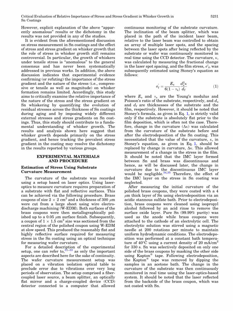
To study the effects of the external stress andstress gradient on whisker growth, a 3-point bend-ing setup was used. First, Sn coatings were elec-trodeposited, using the process described earlier inthe ‘‘Estimation of Stress Using Substrate Curva-ture Measurement’’ section with the same bathtemperature and current density, on only one side ofa 200 lm thick and 5 cm long brass strip. Figure 1schematically illustrates the strategies employed forapplication of external compressive and tensilestresses. The advantages of such a setup are: (1) itallowed the imposed stress and stress gradients tobe quantified using simple finite element analysis(FEA) of a bimetallic strip under bending load, (2)tensile and compressive stress of the same magni-tude can be imposed in the coatings on the oppositesides of the sample at the same time, as shownschematically in Fig. 1, (3) data corresponding tovarious tensile and compressive stresses can beobtained using one experiment, and (4) bending ofthe Sn coating in such a manner also producedstress gradients along the thickness of the coating(and substrate). In particular, as shown in Fig. 1b,the application of stress in such a way created thestress gradients along the thickness direction, suchthat the surface of the Sn coating was at maximumtension or compression, depending on the configu-ration chosen in Fig. 1a.
FEA of the bimetallic strip with geometry similarto that of the actual sample was also employed usingANSYS�, a commercial FEA software package, forquantification of the stress state as well as thestress gradient across the coating thickness imposedby the 3-point bending. FEA was performed byassigning the time independent elastic–plastic prop-erty for Sn. An experimental stress–strain curve ofpure Sn obtained at a constant strain rate of 10�3
s�1 was used for the Sn coating (and hence we do notassume ideal plasticity for Sn in our simulations).The brass substrate was assumed to be elastic,which is reasonable for a thick brass substrate.
After electrodeposition and loading of the sampleinto a 3-point bending fixture, it was stored in a
Jagtap, Sethuraman, and Kumar5232
hot air oven at 50�C and whisker density as well asthe Cu6Sn5 IMC layer was observed after 7 days.The IMC layer was observed by cross-sectionimaging and chemical etching of the Sn coatings.The sample for cross-section examination wasprepared using dual beam focused ion beam (FIB)machining, while the Sn coating was etched awayusing a warm solution of 7 parts o-nitro-phenol and1 part NaOH. Whisker density in the samples wasevaluated at several distances from the center (i.e.,maximum deflection point) and correlated with themagnitude of the stress and stress gradient thatexist at the particular location or correspondingregion.
RESULTS
Substrate Curvature Measurements
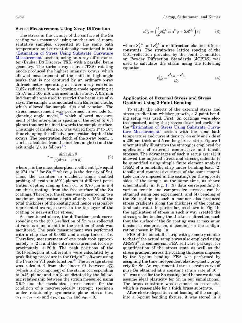
Figure 2 shows the evolution of bulk stress in arepresentative Sn coating aged at room tempera-ture, as estimated using Eq. 1. Careful observationof Fig. 2 readily reveals the following: (1) theresidual stress in the Sn coating immediately afterdeposition was compressive, (2) the initial compres-sive stress in the Sn coatings relaxed rapidly duringthe initial hours of aging following the deposition,(3) thereafter, stress became progressively morecompressive with aging, and (4) the compressivestress showed saturation near � 12 MPa (which isclose to the yield strength of Sn) after 400 h ofaging. Interestingly, whiskers were observed in thissample after just 7 days (i.e., � 180 h), suggestingthat whiskering did not completely stop the build-up of stress in Sn coatings. However, saturation instress or the establishment of a steady-state valuefor stress after 400 h suggests that once a very largenumber of whiskers had nucleated, the stressgenerated due to IMC formation at the substrate-coating interface and the stress relaxation due towhisker growth balanced each other. It should benoted that the measured stress corresponds to theentire Sn coating (i.e., both bulk and surface).However, it is expected that the average value willbe affected more by the volume of the material awayfrom the top surface as compared to the surface andhence the stress shown in Fig. 2 can be assumed torepresent the bulk stress.
Fig. 1. (a) 3-Point bending schemes used to apply external stressand stress gradient on the Sn-coated brass. (b) Schematic illustra-tion of the stress gradient produced as per the schematic shown in(a). The size and the direction of horizontal arrows in (b) denote themagnitude and sign of the dominant stress component in the Sncoating, whereas the thick and broken vertical arrows show thedirection of significant and less-significant atomic transport, respec-tively. The vertical channel (onto which the stresses are shownacting) in (b) represent a columnar grain of Sn coating.
Fig. 2. Bulk stress evolution over time in two 4 lm thick Sn coatingselectrodeposited on a 200 lm thick brass substrate, as measuredusing the laser-optics-based curvature measurement setup. Thevertical line shows the approximate time at which the first set ofwhiskers started to grow in these coatings. Samples were storedunder ambient conditions.
Critical Evaluation of Relative Importance of Stress and Stress Gradient in Whisker Growth inSn Coatings
5233
Stress Measurement Using X-ray Diffraction
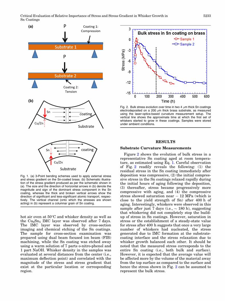
Figure 3a shows the peak profile of the (501)-planes obtained at different angles of incidence. Thevertical arrow in Fig. 3a shows the expected posi-tion of the peak of the (501)-reflection in anunstrained crystal, and any deviation from thisarrow can be attributed to the strain in the sample.Figure 3 clearly shows a significant shift in the peakposition of the (501)-reflection of the Sn coatingafter 5 days of aging. Subsequently, the strainvalues at different incidence angles were plottedagainst sin2w to calculate the average stress in thetop 0.76 lm of the coating. As directed by Eq. 3, thestrain values at different incidence angles, x, andtherefore at different w tilts, were plotted as func-tion of sin2w (see Fig. 3b). As shown in Fig. 3b, areasonably linear fit between the strain and sin2wvalues was obtained. The stress was calculated fromthe slope of the linear fit using Eq. 3. It should becategorically noted that the value of stress reportedfollowing this method is the average stress near thesurface of Sn coatings (i.e., top 0.7 lm of the coating)and does not represent the bulk stress. Conse-quently, stress near the surface region was mea-sured using the aforementioned technique afterdifferent aging times of up to 30 days afterelectrodeposition.
Figure 4 shows the Sin2w plot of the same coating,whose data is shown in Fig. 3, as recorded atdifferent times along with the variation of stresswith time. It can be readily observed from Fig. 4that the stress in the as-deposited samples wascompressive and became less compressive (i.e., moretensile) with aging time. This suggests that whiskergrowth is a surface relief process, such that surfacestress becomes continuously less compressive dur-ing whisker growth. A comparison of Figs. 2 and 4bclearly suggests that the stress gradient in the Sncoating between the bulk and the top layer of thecoating became more negative (i.e., negativelyincreased) with increased storage time. The impli-cation of this observation on whisker growth will bediscussed later.
It should be noted that the effects of thecrystallographic texture and grain interactionbetween polycrystalline grains and the constraintsimposed on neighboring grains were not consid-ered in this XRD stress analysis. The analysisassumes rotationally symmetric equal biaxialstress in Sn and a macroscopically isotropic spec-imen. Furthermore, as whiskers start to a grow ata particular location, the stress state in thevicinity of the whisker grain will change. Suchlocal variation in the stress field was not capturedusing the XRD (as well as curvature measure-ment) analysis performed herein. Nevertheless, itdoes capture the evolution of the average (orglobal) near-surface stress in the Sn coating as afunction of aging time.
Effect of External Stress on Whisker Growth
As discussed in the ‘‘Application of ExternalStress and Stress Gradient Using 3-Point Bending’’section, an external stress along with a stressgradient was imposed on the Sn-coated brass stripsusing a 3-point bending setup. The stress variationin the Sn-coated brass strip at various distancesfrom the center (i.e., point of maximum deflection) isshown in Fig. 5. If the Sn is allowed to deformplastically with negligible hardening, a saturationin stress can be observed. Henceforth, the stressvalues, at different locations along the length of theSn-coated strip reported in this study, are thevalues ‘‘predicted’’ using the FEA model incorporat-ing plasticity. It is noteworthy that the stressesmentioned in Fig. 5 occur at the instant of loading
Fig. 3. (a) Peak profile of the (501)-reflections of the Sn coatingobtained at different incidence angles, x, shown in the legend. Thedata was collected 5 days after the electrodeposition. (b) Strainversus sin2w plot for the Sn coating deposited on brass as recordedafter 5 days after electrodeposition. The legend shows the equationobtained from the best linear curve fit, along with the curve fittingparameter, R. The sample was stored under ambient condition.
Jagtap, Sethuraman, and Kumar5234
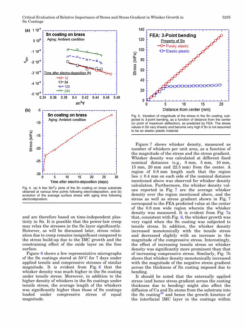
and are therefore based on time-independent plas-ticity in Sn. It is possible that the power-law creepmay relax the stresses in the Sn layer significantly.However, as will be discussed later, stress relax-ation due to creep remains insignificant compared tothe stress build-up due to the IMC growth and theconstraining effect of the oxide layer on the freesurface.
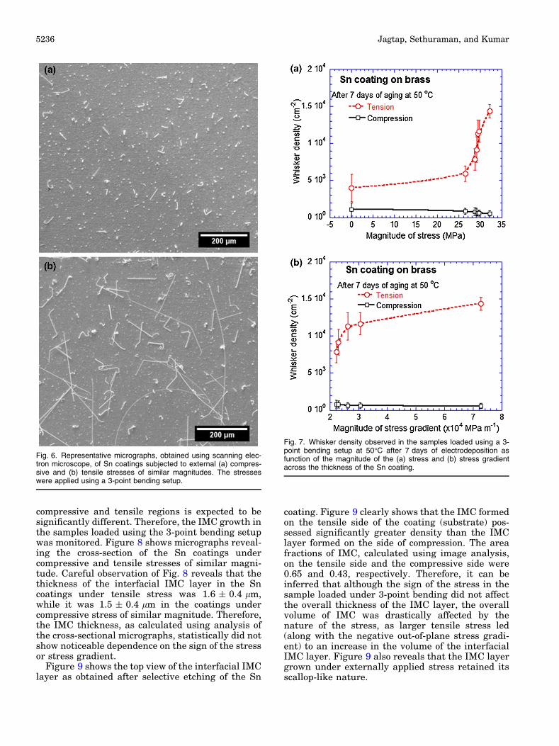
Figure 6 shows a few representative micrographsof the Sn coatings stored at 50�C for 7 days underapplied tensile and compressive stresses of similarmagnitude. It is evident from Fig. 6 that thewhisker density was much higher in the Sn coatingunder tensile stress. Moreover, in addition to thehigher density of whiskers in the Sn coatings undertensile stress, the average length of the whiskerswas significantly higher than those of Sn coatingsloaded under compressive stress of equalmagnitude.
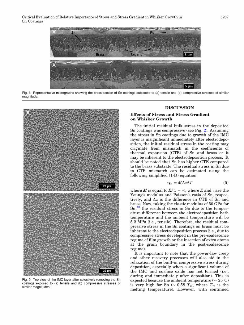
Figure 7 shows whisker density, measured asnumber of whiskers per unit area, as a function ofthe magnitude of the stress and the stress gradient.Whisker density was calculated at different fixednominal distances (e.g., 0 mm, 5 mm, 10 mm,15 mm, 20 mm and 22.5 mm) from the center. Aregion of 0.8 mm length such that the regionlies ± 0.4 mm on each side of the nominal distancementioned above was observed for whisker densitycalculation. Furthermore, the whisker density val-ues reported in Fig. 7 are the average whiskerdensity over the region mentioned above, and thestress as well as stress gradient shown in Fig. 7correspond to the FEA predicted value at the centerof the 0.8 mm wide region wherein the whiskerdensity was measured. It is evident from Fig. 7athat, consistent with Fig. 6, the whisker growth wasvery rapid when the Sn coating was subjected totensile stress. In addition, the whisker densityincreased monotonically with the tensile stressand decreased slightly with an increase in themagnitude of the compressive stress. Interestingly,the effect of increasing tensile stress on whiskerdensity was significantly more prominent than thatof increasing compressive stress. Similarly, Fig. 7bshows that whisker density monotonically increasedwith the magnitude of the negative stress gradientacross the thickness of Sn coating imposed due tobending.
It should be noted that the externally appliedstress (and hence stress gradient across the coatingthickness due to bending) might also affect thediffusion of Cu and Zn atoms from the substrate intothe Sn coating39 and hence the growth kinetics ofthe interfacial IMC layer in the coatings within
Fig. 4. (a) A few Sin2w plots of the Sn coating on brass substrateobtained at various time points following electrodeposition, and (b)evolution of the average surface stress with aging time followingelectrodeposition.
Fig. 5. Variation of magnitude of the stress in the Sn coating, sub-jected to 3-point bending, as a function of distance from the center(or point of maximum deflection), as predicted by FEA. The stressvalues in Sn vary linearly and become very high if Sn is not assumedto be an elastic–plastic material.
Critical Evaluation of Relative Importance of Stress and Stress Gradient in Whisker Growth inSn Coatings
5235
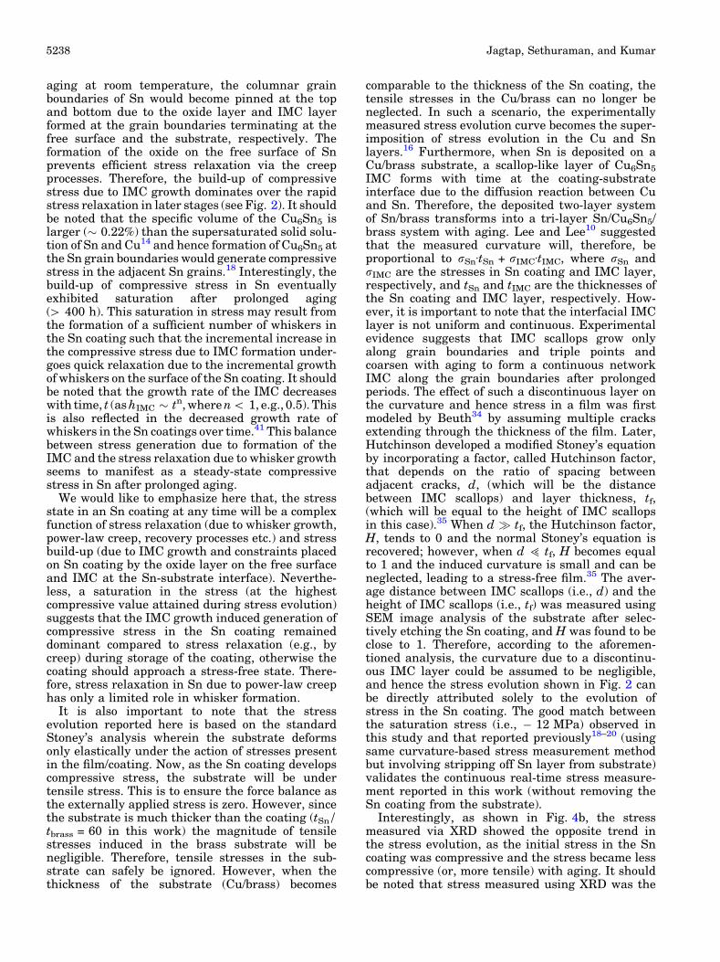
compressive and tensile regions is expected to besignificantly different. Therefore, the IMC growth inthe samples loaded using the 3-point bending setupwas monitored. Figure 8 shows micrographs reveal-ing the cross-section of the Sn coatings undercompressive and tensile stresses of similar magni-tude. Careful observation of Fig. 8 reveals that thethickness of the interfacial IMC layer in the Sncoatings under tensile stress was 1.6 ± 0.4 lm,while it was 1.5 ± 0.4 lm in the coatings undercompressive stress of similar magnitude. Therefore,the IMC thickness, as calculated using analysis ofthe cross-sectional micrographs, statistically did notshow noticeable dependence on the sign of the stressor stress gradient.
Figure 9 shows the top view of the interfacial IMClayer as obtained after selective etching of the Sn
coating. Figure 9 clearly shows that the IMC formedon the tensile side of the coating (substrate) pos-sessed significantly greater density than the IMClayer formed on the side of compression. The areafractions of IMC, calculated using image analysis,on the tensile side and the compressive side were0.65 and 0.43, respectively. Therefore, it can beinferred that although the sign of the stress in thesample loaded under 3-point bending did not affectthe overall thickness of the IMC layer, the overallvolume of IMC was drastically affected by thenature of the stress, as larger tensile stress led(along with the negative out-of-plane stress gradi-ent) to an increase in the volume of the interfacialIMC layer. Figure 9 also reveals that the IMC layergrown under externally applied stress retained itsscallop-like nature.
Fig. 6. Representative micrographs, obtained using scanning elec-tron microscope, of Sn coatings subjected to external (a) compres-sive and (b) tensile stresses of similar magnitudes. The stresseswere applied using a 3-point bending setup.
Fig. 7. Whisker density observed in the samples loaded using a 3-point bending setup at 50�C after 7 days of electrodeposition asfunction of the magnitude of the (a) stress and (b) stress gradientacross the thickness of the Sn coating.
Jagtap, Sethuraman, and Kumar5236
DISCUSSION
Effects of Stress and Stress Gradienton Whisker Growth
The initial residual bulk stress in the depositedSn coatings was compressive (see Fig. 2). Assumingthe stress in Sn coatings due to growth of the IMClayer is insignificant immediately after electrodepo-sition, the initial residual stress in the coating mayoriginate from mismatch in the coefficients ofthermal expansion (CTE) of Sn and brass or itmay be inherent to the electrodeposition process. Itshould be noted that Sn has higher CTE comparedto the brass substrate. The residual stress in Sn dueto CTE mismatch can be estimated using thefollowing simplified (1-D) equation:
rSn ¼ MDaDT ð5Þ
where M is equal to E/(1 � m), where E and m are theYoung’s modulus and Poisson’s ratio of Sn, respec-tively, and Da is the difference in CTE of Sn andbrass. Now, taking the elastic modulus of 50 GPa forSn,40 the residual stress in Sn due to the temper-ature difference between the electrodeposition bathtemperature and the ambient temperature will be5.2 MPa (i.e., tensile). Therefore, the residual com-pressive stress in the Sn coatings on brass must beinherent to the electrodeposition process (i.e., due tocompressive stress developed in the pre-coalescenceregime of film growth or the insertion of extra atomsat the grain boundary in the post-coalescenceregime).
It is important to note that the power-law creepand other recovery processes will also aid in therelaxation of the built-in compressive stress duringdeposition, especially when a significant volume ofthe IMC and surface oxide has not formed (i.e.,during and immediately after deposition). This isexpected because the ambient temperature (� 25�C)is very high for Sn (� 0.58 Tm, where Tm is themelting temperature). However, with continued
Fig. 8. Representative micrographs showing the cross-section of Sn coatings subjected to (a) tensile and (b) compressive stresses of similarmagnitude.
Fig. 9. Top view of the IMC layer after selectively removing the Sncoatings exposed to (a) tensile and (b) compressive stresses ofsimilar magnitudes.
Critical Evaluation of Relative Importance of Stress and Stress Gradient in Whisker Growth inSn Coatings
5237
aging at room temperature, the columnar grainboundaries of Sn would become pinned at the topand bottom due to the oxide layer and IMC layerformed at the grain boundaries terminating at thefree surface and the substrate, respectively. Theformation of the oxide on the free surface of Snprevents efficient stress relaxation via the creepprocesses. Therefore, the build-up of compressivestress due to IMC growth dominates over the rapidstress relaxation in later stages (see Fig. 2). It shouldbe noted that the specific volume of the Cu6Sn5 islarger (� 0.22%) than the supersaturated solid solu-tion of Sn and Cu14 and hence formation of Cu6Sn5 atthe Sn grain boundaries would generate compressivestress in the adjacent Sn grains.18 Interestingly, thebuild-up of compressive stress in Sn eventuallyexhibited saturation after prolonged aging(> 400 h). This saturation in stress may result fromthe formation of a sufficient number of whiskers inthe Sn coating such that the incremental increase inthe compressive stress due to IMC formation under-goes quick relaxation due to the incremental growthof whiskers on the surface of the Sn coating. It shouldbe noted that the growth rate of the IMC decreaseswith time, t (ashIMC � tn, wheren< 1, e.g., 0.5). Thisis also reflected in the decreased growth rate ofwhiskers in the Sn coatings over time.41 This balancebetween stress generation due to formation of theIMC and the stress relaxation due to whisker growthseems to manifest as a steady-state compressivestress in Sn after prolonged aging.
We would like to emphasize here that, the stressstate in an Sn coating at any time will be a complexfunction of stress relaxation (due to whisker growth,power-law creep, recovery processes etc.) and stressbuild-up (due to IMC growth and constraints placedon Sn coating by the oxide layer on the free surfaceand IMC at the Sn-substrate interface). Neverthe-less, a saturation in the stress (at the highestcompressive value attained during stress evolution)suggests that the IMC growth induced generation ofcompressive stress in the Sn coating remaineddominant compared to stress relaxation (e.g., bycreep) during storage of the coating, otherwise thecoating should approach a stress-free state. There-fore, stress relaxation in Sn due to power-law creephas only a limited role in whisker formation.
It is also important to note that the stressevolution reported here is based on the standardStoney’s analysis wherein the substrate deformsonly elastically under the action of stresses presentin the film/coating. Now, as the Sn coating developscompressive stress, the substrate will be undertensile stress. This is to ensure the force balance asthe externally applied stress is zero. However, sincethe substrate is much thicker than the coating (tSn/tbrass = 60 in this work) the magnitude of tensilestresses induced in the brass substrate will benegligible. Therefore, tensile stresses in the sub-strate can safely be ignored. However, when thethickness of the substrate (Cu/brass) becomes
comparable to the thickness of the Sn coating, thetensile stresses in the Cu/brass can no longer beneglected. In such a scenario, the experimentallymeasured stress evolution curve becomes the super-imposition of stress evolution in the Cu and Snlayers.16 Furthermore, when Sn is deposited on aCu/brass substrate, a scallop-like layer of Cu6Sn5
IMC forms with time at the coating-substrateinterface due to the diffusion reaction between Cuand Sn. Therefore, the deposited two-layer systemof Sn/brass transforms into a tri-layer Sn/Cu6Sn5/brass system with aging. Lee and Lee10 suggestedthat the measured curvature will, therefore, beproportional to rSnÆtSn + rIMCÆtIMC, where rSn andrIMC are the stresses in Sn coating and IMC layer,respectively, and tSn and tIMC are the thicknesses ofthe Sn coating and IMC layer, respectively. How-ever, it is important to note that the interfacial IMClayer is not uniform and continuous. Experimentalevidence suggests that IMC scallops grow onlyalong grain boundaries and triple points andcoarsen with aging to form a continuous networkIMC along the grain boundaries after prolongedperiods. The effect of such a discontinuous layer onthe curvature and hence stress in a film was firstmodeled by Beuth34 by assuming multiple cracksextending through the thickness of the film. Later,Hutchinson developed a modified Stoney’s equationby incorporating a factor, called Hutchinson factor,that depends on the ratio of spacing betweenadjacent cracks, d, (which will be the distancebetween IMC scallops) and layer thickness, tf,(which will be equal to the height of IMC scallopsin this case).35 When d � tf, the Hutchinson factor,H, tends to 0 and the normal Stoney’s equation isrecovered; however, when d > tf, H becomes equalto 1 and the induced curvature is small and can beneglected, leading to a stress-free film.35 The aver-age distance between IMC scallops (i.e., d) and theheight of IMC scallops (i.e., tf) was measured usingSEM image analysis of the substrate after selec-tively etching the Sn coating, and H was found to beclose to 1. Therefore, according to the aforemen-tioned analysis, the curvature due to a discontinu-ous IMC layer could be assumed to be negligible,and hence the stress evolution shown in Fig. 2 canbe directly attributed solely to the evolution ofstress in the Sn coating. The good match betweenthe saturation stress (i.e., � 12 MPa) observed inthis study and that reported previously18–20 (usingsame curvature-based stress measurement methodbut involving stripping off Sn layer from substrate)validates the continuous real-time stress measure-ment reported in this work (without removing theSn coating from the substrate).
Interestingly, as shown in Fig. 4b, the stressmeasured via XRD showed the opposite trend inthe stress evolution, as the initial stress in the Sncoating was compressive and the stress became lesscompressive (or, more tensile) with aging. It shouldbe noted that stress measured using XRD was the
Jagtap, Sethuraman, and Kumar5238
average stress in only the top 0.7 lm layer of the Sncoating. It is now known that under ambientconditions, Sn forms a stable oxide SnO2. SinceSnO2 has a higher molar volume than Sn,42 forma-tion of SnO2 along Sn grain boundaries terminatingon the free surface, where diffusion of oxygen isfaster,42 will induce compressive stress near thesurface of the Sn coating. Since the oxide layer isvery thin, the compressive stresses will only beinduced in the topmost regions. Now, the decreasein the compressive stress in the top layer with timecan be explained as follows: (1) disruption of theSnO2 layer along grain boundaries of Sn due tonucleation and growth of whiskers, and (2) replace-ment of SnO2 by more stable ZnO. ZnO forms due tothe fast diffusion of Zn atoms from the brasssubstrate along the grain boundaries of Sn and thesubsequent reaction with SnO2. The fast diffusion ofZn was confirmed using electron probe microanal-ysis (EPMA) in one of our previous studies41 andalso in a few other studies,43,44 where a considerableZn concentration was observed near the free surfaceof the Sn coating. The molar volume of ZnO is14.5 cm3/mol,45 which is considerably less than themolar volume of SnO2, which is 21.7 cm3/mol.42
Therefore, replacing SnO2 with ZnO will relax theexisting compressive stress near the surface of thecoatings. In summary, formation of ZnO throughthe reaction between SnO2 and Zn and disruption ofthe oxide layer explains the decrease in the com-pressive stress near the surface of the Sn coatingswith time. Therefore, it can be inferred that themechanisms of stress generation and stress relax-ation at the coating-substrate interface and at thefree surface in the Sn coating, respectively, arefundamentally different.
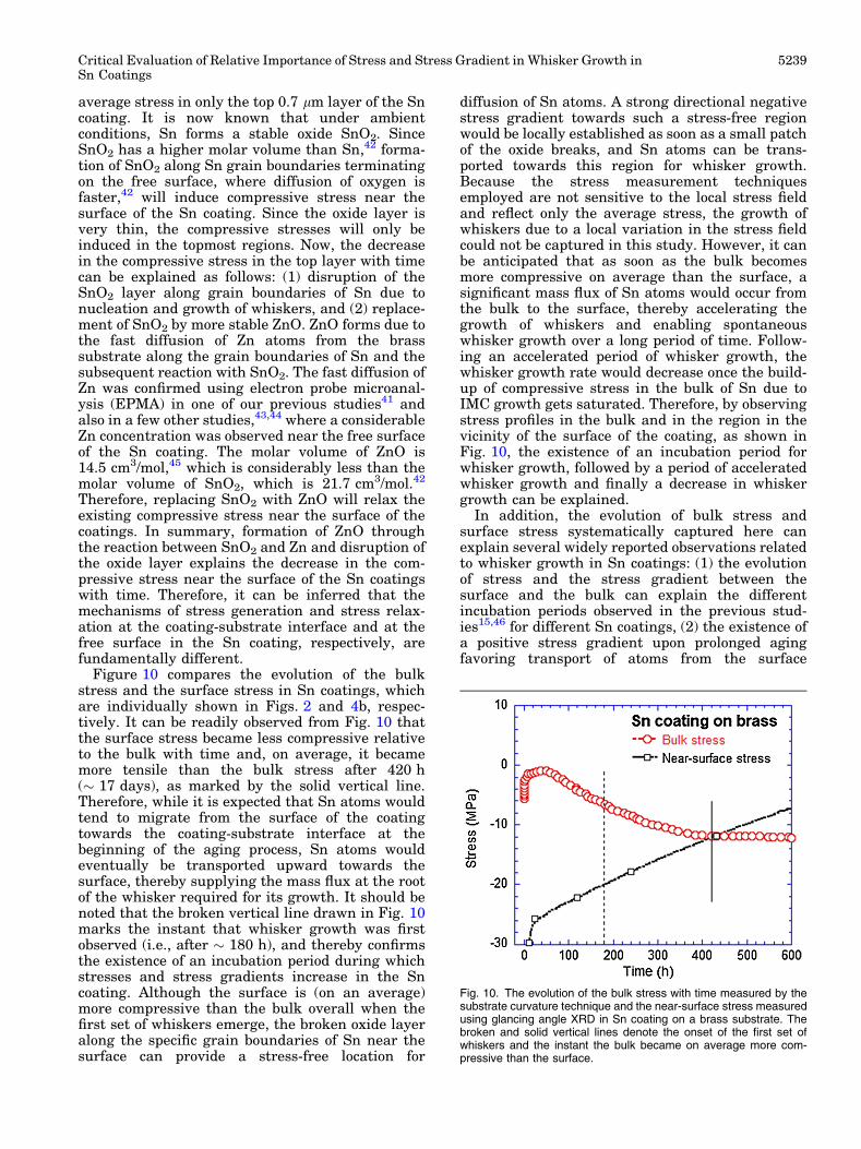
Figure 10 compares the evolution of the bulkstress and the surface stress in Sn coatings, whichare individually shown in Figs. 2 and 4b, respec-tively. It can be readily observed from Fig. 10 thatthe surface stress became less compressive relativeto the bulk with time and, on average, it becamemore tensile than the bulk stress after 420 h(� 17 days), as marked by the solid vertical line.Therefore, while it is expected that Sn atoms wouldtend to migrate from the surface of the coatingtowards the coating-substrate interface at thebeginning of the aging process, Sn atoms wouldeventually be transported upward towards thesurface, thereby supplying the mass flux at the rootof the whisker required for its growth. It should benoted that the broken vertical line drawn in Fig. 10marks the instant that whisker growth was firstobserved (i.e., after � 180 h), and thereby confirmsthe existence of an incubation period during whichstresses and stress gradients increase in the Sncoating. Although the surface is (on an average)more compressive than the bulk overall when thefirst set of whiskers emerge, the broken oxide layeralong the specific grain boundaries of Sn near thesurface can provide a stress-free location for
diffusion of Sn atoms. A strong directional negativestress gradient towards such a stress-free regionwould be locally established as soon as a small patchof the oxide breaks, and Sn atoms can be trans-ported towards this region for whisker growth.Because the stress measurement techniquesemployed are not sensitive to the local stress fieldand reflect only the average stress, the growth ofwhiskers due to a local variation in the stress fieldcould not be captured in this study. However, it canbe anticipated that as soon as the bulk becomesmore compressive on average than the surface, asignificant mass flux of Sn atoms would occur fromthe bulk to the surface, thereby accelerating thegrowth of whiskers and enabling spontaneouswhisker growth over a long period of time. Follow-ing an accelerated period of whisker growth, thewhisker growth rate would decrease once the build-up of compressive stress in the bulk of Sn due toIMC growth gets saturated. Therefore, by observingstress profiles in the bulk and in the region in thevicinity of the surface of the coating, as shown inFig. 10, the existence of an incubation period forwhisker growth, followed by a period of acceleratedwhisker growth and finally a decrease in whiskergrowth can be explained.
In addition, the evolution of bulk stress andsurface stress systematically captured here canexplain several widely reported observations relatedto whisker growth in Sn coatings: (1) the evolutionof stress and the stress gradient between thesurface and the bulk can explain the differentincubation periods observed in the previous stud-ies15,46 for different Sn coatings, (2) the existence ofa positive stress gradient upon prolonged agingfavoring transport of atoms from the surface
Fig. 10. The evolution of the bulk stress with time measured by thesubstrate curvature technique and the near-surface stress measuredusing glancing angle XRD in Sn coating on a brass substrate. Thebroken and solid vertical lines denote the onset of the first set ofwhiskers and the instant the bulk became on average more com-pressive than the surface.
Critical Evaluation of Relative Importance of Stress and Stress Gradient in Whisker Growth inSn Coatings
5239
towards the interface can explain depletion zones orsubsiding grains reported in the literature,30,47 and(3) cross-over of bulk stress and surface stressproducing negative stress gradients favoring masstransport of atoms from compressive regions nearthe IMC towards the whisker root can explain thecontinued growth of whiskers over time.
Effect of Externally Imposed Stress and StressGradient on Whisker Growth
As discussed in the previous section, both the near-surface and the bulk stresses and the produced stressgradients play critical roles in whisker growth. Theexternally applied stress, as shown in Fig. 1, will alsoaffect the stress state in the top layer of the coating, sothat the Sn coating subjected to the outward bending(i.e., convex side) will have the maximum tensilestress at the surface and the inward bent (i.e.,concave side) coating will have the maximum com-pressive stress at the coating surface. Therefore, anegative stress gradient, necessary for whiskergrowth, was inherently imposed in the Sn coatingsthat are outward bent, which are under tensile stress.The direction of such a stress gradient will bereversed for the inward bent coatings. Based ondiscussion presented in the section ‘‘Effects of Stressand Stress Gradient on Whisker Growth’’, this makesthe outward bent coatings, i.e., the coatings undertensile stress, more prone to whisker growth.
In addition, it was shown in Figs. 8 and 9 thatalthough the thickness (i.e., growth rate) of theinterfacial IMC layer was similar in coatings loadedunder tensile and compressive stresses, the volume ofIMC formed (i.e., nucleation rate of IMC) in thecoatings under tension was significantly greater thanthat of coatings under compression. The enhancednucleation of IMC in the Sn coatings loaded undertensile stress can be attributed to the fact that most ofthe columnar grain boundaries of Sn terminating onthe substrate experienced a tensile opening force.This enhances the diffusion of Cu atoms and subse-quent nucleation of IMC as compared to the Sncoating loaded under compressive stress, whereinmost of the boundaries experience a compressivestress (see Fig. 1b for schematic illustration). As soonas the interfacial IMC starts to grow, the negativestress gradient in the outward bent coating will befurther augmented by the additional influence of theintrinsically generated compressive stress due to theformation of interfacial IMC along Sn grain bound-aries. Interestingly, the externally applied tensilestress in the outward bent coating will also break the(brittle) surface oxide layer at several locations, thusincreasing the probable sites of whisker growth aswell as adding to the existing outward stress gradi-ent. This is in good agreement with the observationthat whiskers were longer and grew at a higher ratein outward bent coatings, which were simultaneouslyunder tensile stress, relative to the inward bentcoatings.
It should be noted that a similar observationpertaining to the enhanced whisker growth undertensile stress was also reported by Chen et al.15
Crandall et al.29 and Cheng et al.30 However,explanation for these observations was lacking.This work presents a systematic variation in thewhisker density as a function of tensile as well ascompressive stress, and, more importantly, alsoexplains the whisker growth under tensile stressby considering the stress gradient. It is apparentfrom the evidence provided in this study that thenegative stress gradient, as opposed to stress,dominantly governs whisker growth in Sncoatings.
Although we observe an important role for thenegative out-of-plane stress gradient in this work, itis important to highlight here that we did notmeasure the in-plane stress gradients in the Snlayer and hence cannot conclusively say that out-of-plane stress gradients are more important than in-plane stress gradients. However, there are severalexperimental reports which use synchrotron x-raymicro-diffraction to measure stress/strain gradientsaround the whiskering site that show that long-range in-plane stress gradients are not very promi-nent and unique to whisker grain,.48,49 The crystalplasticity simulations based on EBSD grain orien-tation maps around whisker grain also indicate thein-plane stress gradients are only short-range andnot uniquely prominent around whisker grain.50
Additionally, Kehrer and Kadereit51 showed usingradioactive tracer experiments that when an inac-tive Sn layer was deposited on top of a radioactiveSn layer, the whiskers formed on the top surface ofthe inactive Sn layer were composed of radioactiveSn. This observation confirms that vertical masstransport is more critical than the lateral masstransport. In light of all the experimental andtheoretical evidence, we infer that out-of-planestress gradients play a more important role in thewhisker growth process than the nature of thestress alone.
CONCLUSIONS
� The stress state in Sn coatings on brass wasstudied using two techniques, substrate curva-ture measurement using laser-optics and glanc-ing x-ray diffraction. The curvature techniqueallowed measurement of average bulk stresses inSn and its evolution with aging. Similarly, theglancing angle x-ray diffraction allowed mea-surement of average stress in the top � 0.7 lmlayer near the free surface of the coating and itsevolution with aging.
� The near-surface and bulk stresses in the Sncoating evolved differently with time. The bulkstress in the Sn was compressive immediatelyafter electrodeposition; however, it rapidly re-laxed and thereafter progressively became morecompressive due to IMC growth until stress
Jagtap, Sethuraman, and Kumar5240
build-up due to IMC formation was balanced bystress relaxation by whisker formation. This ledto saturation in stress values. In contrast, stressin the Sn layer near the top surface of thecoating became less compressive (i.e., moretensile) with time.
� Initially, a positive stress gradient (i.e., thecoating substrate interface was more tensilethan the surface) was observed in the Sn;however, the sign of this gradient reversed aftera certain aging period (i.e., 400 h at roomtemperature), enabling a dramatic increase inthe transport of Sn atoms from the highly-compressed Sn layer near the IMC to thewhisker root.
� Whisker density increased monotonically withexternally imposed tensile stress and negativestress gradient. The enhanced whisker growthwas due to the combined effects of the ease ofdisrupting the surface oxide layer at multiplelocations and a negative stress gradient towardsthese locations that is inherent to such outwardbent (or tensile loaded) Sn coatings.
� The externally imposed tensile stress along withthe negative stress gradient accelerated the IMCgrowth such that the density of IMC observed inSn coatings under tensile stress with a negativestress gradient was higher than that for coatingsunder compressive stress with a positive stressgradient.
ACKNOWLEDGEMENTS
This work was financially supported by the In-dian Space Research Organization (ISRO) throughthe Space Technology Cell at the Indian Institute ofScience, Bangalore (Grant # ISTC 0367). Discus-sions with Dr. Ramesh Narayan P. of VikramSarabhai Space Centre, Indian Space Organisation,Trivandrum are also acknowledged. We also thankProfessor Rajeev Ranjan and Dr. Amit Sharma ofIndian Institute of Science, Bangalore for their helpwith XRD.
REFERENCES
1. H. Leidecker and J. Brusse, Tin whiskers: a history ofdocumented electrical system failures (2006). Online at:http://nepp.nasa.gov/whisker.
2. R.M. Fisher, L.S. Darken, and K.G. Carroll, Acta Metall.Mater. 2, 368 (1954).
3. V.K. Glazunova and N.T. Kudryavtsev, Translated fromZhurnal Prikladnoi Khimii 36, 543 (1963).
4. U. Lindborg, Metall. Trans. A 6, 1581 (1975).5. C.H. Pitt and R.G. Henning, J. Appl. Phys. 35, 459 (1964).6. M. Sobiech, M. Wohlschlogel, U. Welzel, E.J. Mittemeijer,
W. Hugel, A. Seekamp, W. Liu, and G.E. Ice, Appl. Phys.Lett. 94, 221901 (2009).
7. K.N. Tu, Acta Metall. 21, 347 (1973).
8. C. Xu, Y. Zhang, C. Fan, A. Vysotskaya, J. Abys, L. Hop-kins, and N.F. Stevie, in Proc. AESF SUR/FIN Conf., Jun.2001.
9. R. Schetty, N. Brown, A. Egli, J. Heber, and A. Vinckler, inProc. AESF SUR/FIN Conf., (2001) 1.
10. B.Z. Lee and D.N. Lee, Acta Mater. 46, 3701 (1998).11. S. Lal and T.D. Moyer, IEEE Trans. Electron. Packag.
Manuf. 28, 63 (2005).12. U. Welzel and E.J. Mittemeijer, in Defect and Diffusion
Forum, Trans Tech Publications 264 (2007) 71.13. M. Sobiech, U. Welzel, E.J. Mittemeijer, W. Hugel, and A.
Seekamp, Appl. Phys. Lett. 93, 011906-1-3. (2008).14. W.J. Boettinger, C.E. Johnson, L.A. Bendersky, K.W.
Moon, M.E. Williams, and G.R. Stafford, Acta Mater. 53,305033 (2005).
15. K. Chen and G.D. Wilcox, Phys. Rev. Lett. 94, 066104(2005).
16. E. Chason, L. Reinbold, and S. Kumar, in MRS Proc.,Cambridge University Press, 851 (2004) NN5171.
17. E. Chason, N. Jadhav, W.L. Chan, L. Reinbold, and K.S.Kumar, Appl. Phys. Lett. 92, 171901 (2008).
18. E. Chason, N. Jadhav, and F. Pei, JOM 63, 62 (2011).19. N. Jadhav, J. Wasserman, F. Pei, and E. Chason, J. Elec-
tron. Mater. 41, 588 (2012).20. E. Chason and F. Pei, JOM 67, 2416 (2015).21. K.N. Tu and J.C. Li, Mater. Sci. Eng. A 409, 131 (2005).22. P. Su, M. Ding, and S. Chopin, in Proc. Electron. Comp.
And Tech. Conf., (ECTC) (2005) 434–440.23. K.N. Tu, C. Chen, and A.T. Wu, J. Mater. Sci. Mater.
Electron. 18, 269 (2007).24. J. Liang, Z.H. Xu, and X. Li, J. Mater. Sci. Mater. Electron.
18, 599 (2007).25. V.K. Glazunova, Transl. Kristallografiya 7, 761 (1962).26. B.D. Dunn, W.R. Burke, and B. Battrick, A laboratory
study of tin whisker growth, European Space Agency (ESA)Rep. STR-223 (1987).
27. C. Xu, Y. Zhang, C. Fan, J. Abys, L. Hopkins, and F. Stevie,Circuit Tree (USA) 15, 10 (2002).
28. S.K. Lin, Y. Yorikado, J. Jiang, K.S. Kim, K. Suganuma,S.W. Chen, M. Tsujimoto, and I. Yanada, J. Mater. Res. 22,1975 (2007).
29. E.R. Crandall, G.T. Flowers, R. Jackson, P. Lall, and M.J.Bozack, in IEEE 57th Conference on Electrical Contacts,Holm (2011) 1.
30. J. Cheng, Tin Whiskers in Electronic Packaging: Mecha-nism and Modeling, PhD thesis, University of Rochester(2011) 83.
31. P. Jagtap, Whisker Growth from Electrodeposited SnCoatings- Developing Materials Science and MechanicsBased Insights, PhD thesis, Indian Institute of Science(2017).
32. J. A. Floro and E. Chason, in In-Situ Real-Time Charac-terization of Thin Films, Ed. O. Auciello and A. R. Krauss,John Wiley and Sons, Inc. (2001) 191.
33. V.A. Sethuraman, M.J. Chon, M. Shimshak, V. Srinivasan,and P.R. Guduru, J. Power Sources 195, 5062 (2010).
34. J.L. Beuth, Int. J. Solids Structures 29, 1657 (1992).35. W.D. Nix, Mechanical properties of thin films, Lecture
notes (2005) Available online at: http://imechanica.org/files/353ClassNotes2005.pdf.
36. U. Welzel, J. Ligot, P. Lamparter, A.C. Vermeulen, andE.J. Mittemeijer, J. Appl. Crystallogr. 38, 1 (2005).
37. A. Kumar, U. Welzel, and E.J. Mittemeijer, J. Appl. Crys-tallogr. 39, 633 (2006).
38. B. D. Cullity, Elements of x-ray Diffraction, Add1son-Wesley Publishing Company, Inc. (1956) 466.
39. Y.C. Cheng, Y.T. Wang, F.C. Hsu, F.C. Lu, C.L. Wu, andM.T. Lin, J. Electron. Mater. 44, 604 (2015).
40. W.F. Gale and T.C. Totemeier, eds., Smithells metals refer-ence book (Oxford: Butterworth-Heinemann, 2003), p. 1373.
41. P. Jagtap and P. Kumar, J. Electron. Mater. 44, 1206(2015).
Critical Evaluation of Relative Importance of Stress and Stress Gradient in Whisker Growth inSn Coatings
5241

42. J.W. Osenbach, J.M. DeLucca, B.D. Potteiger, A. Amin,R.L. Shook, and F.A. Baiocchi, IEEE Trans. Electron.Packag. Manuf. 30, 23 (2007).
43. M.A. Ashworth, G.D. Wilcox, R.L. Higginson, R.J. Heath,and C. Liu, J. Electron. Mater. 43, 1005 (2014).
44. S.C. Britton and M. Clarke, Trans. Inst. Metal Finish. 40, 205(1964).
45. F. Han, W.C. Li, C. Lei, B. He, K. Oshida, and A.H. Lu,Small 10, 2637 (2014).
46. E. Bradley, C.A. Handwerker, J. Bath, R.D. Parker, andR.W. Gedney, Lead-free electronics: iNEMI projects lead tosuccessful manufacturing, John Wiley & Sons (2007) 305.
47. Y. Wang, J.E. Blendell, and C.A. Handwerker, J. Mater.Sci. 49, 1099 (2014).
48. W.J. Choi, T.Y. Lee, K.N. Tu, N. Tamura, R.S. Celestre,A.A. MacDowell, Y.Y. Bong, and L. Nguyen, Acta Mater.51, 6253 (2003).
49. F. Pei, N. Jadhav, E. Buchovecky, A.F. Bower, E. Chason,W. Liu, J.Z. Tischler, G.E. Ice, and R. Xu, J. Appl. Phys.119, 105302 (2016).
50. P. Jagtap, A. Chakraborty, P. Eisenlohr, and P. Kumar,Acta Mater. 134, 346 (2017).
51. H.P. Kehrer and H.G. Kadereit, Appl. Phys. Lett. 16, 411(1970).
Jagtap, Sethuraman, and Kumar5242