
Digital Design using VHDL and Xilinx FPGA. VHDL based synthesis.

CPE/EE 427, CPE 527, VLSI Design I: VHDL design simulation, synthesis, and ASIC flow, Laboratory #8,
Joel Wilder and Aleksandar Milenkovic, ECE Dept., The University of Alabama in Huntsville
1. INTRODUCTION This tutorial steps you through the process of taking a vhdl design, simulating it using
NCLaunch, synthesizing it using Build Gates, re-simulating the gate-level netlist, and then
performing auto place-and-route to achieve a finished ASIC. Pads can also be added to your
design as shown in previous tutorials. Thus, the vhdl-to-ASIC work flow is illustrated.
You will perform this work based on the 0.5um AMI nwell process (lambda = 0.30um).
2. PREPARE THE CADENCE TOOLS From your home directory, change directories into your cadence working directory:
% cd cadence
Make a directory for lab8 and change into that directory:
% mkdir lab8
% cd lab8
Initialize the cadence tools:
% uah-cadence-setup
3. VHDL SIMULATION USING NCLAUNCH First, download the vhdl files you will use for this tutorial (available at http://www.ece.uah.edu/~milenka/cpe527-05F/labs/):
• mu0.vhd -- contains a vhdl description of the mu0 processor
(to learn more about mu0 processor visit http://www.ece.uah.edu/%7Elacasa/tutorials/mu0/mu0desc_files/frame.htm )
• tb_mu0.vhd -- testbench for mu0 component
Next, start NCLaunch in a terminal window at the unix prompt:
% nclaunch -new
What is NCLaunch?

VLSI Design I, Lab 8
Page 2 of 17
NCLaunch is a graphical user interface that helps you manage large design projects and lets you configure and launch your Cadence simulation tools.
NCLaunch is integrated into the Cadence Interleaved Native Compiled Architecture (INCA) and is a component of the SimVision analysis environment.
Want to learn more? Read the NCLaunch User Guide; it is intended for customers who want to simulate Verilog, VHDL, or mixed-language designs using the NCLaunch tool. This manual explains the complete functionality of the tool and gives examples of simulating with NCLaunch. In addition, it serves as a reference guide for finding specific details on using NCLaunch.
Select Multiple Step in the NCLaunch pop-up window:
The first step in the process of compiling the design units is to associate them with libraries.
Select Create cds.lib File… in the Open Design Window and then select Save:
VLSI Design I, Lab 8
Page 3 of 17
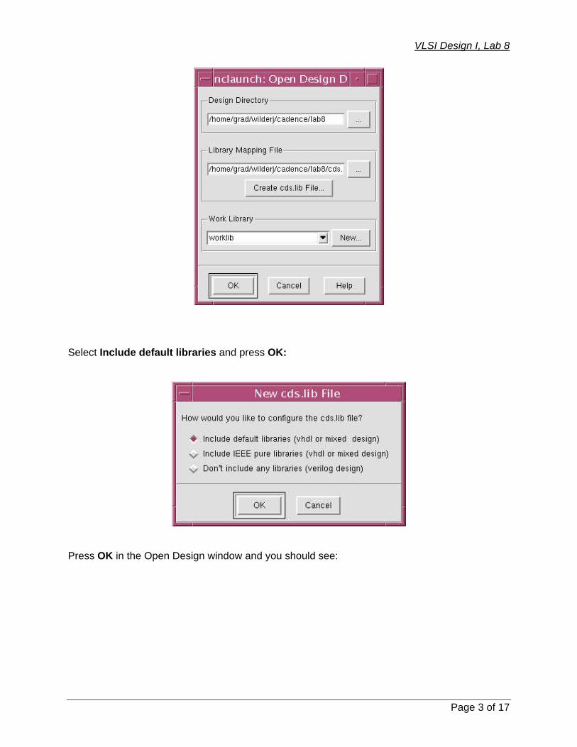
Select Include default libraries and press OK:
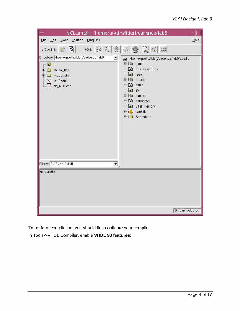
Press OK in the Open Design window and you should see:
VLSI Design I, Lab 8
Page 4 of 17
To perform compilation, you should first configure your compiler.
In Tools->VHDL Compiler, enable VHDL 93 features:

VLSI Design I, Lab 8
Page 5 of 17
Next, select the design units in the correct order (from the lowest design units to the top level units – i.e., select your testbench file last), and in the NCLaunch toolbar click on the VHDL compile icon (passing over the icon you will see the following text: 'Launch VHDL compiler with current settings'):

VLSI Design I, Lab 8
Page 6 of 17
The status should indicate the successful completion of the compilation process.
To perform Elaboration, expand worklib and the design units in it. Select the top level design unit (usually testbench, in our case tb_mu0) and select its entity:

VLSI Design I, Lab 8
Page 7 of 17
Click on the Elaborator icon on the menu.
The status should indicate the successful completion of the elaboration phase.
For simulation, expand the Snapshots directory and select the testbench. Then, click on the Simulation icon on the menu to get the simulation environment loaded:
The SimVison console and Design Browser windows will appear:

VLSI Design I, Lab 8
Page 8 of 17
In the Design Browser window, select the top level entity:

VLSI Design I, Lab 8
Page 9 of 17
Select the signals you want to inspect:

VLSI Design I, Lab 8
Page 10 of 17
Click on the 'waveform' icon on the menu to bring up the waveform window. In the SimVison console, type run 10000 ns; as shown:

VLSI Design I, Lab 8
Page 11 of 17
Inspect the waveforms to ensure the design is working properly.
Other cool options:
Click on the 'schematic' icon on the menu to bring up the schematic tracer:

VLSI Design I, Lab 8
Page 12 of 17
4. VHDL SYNTHESIS TO GATE-LEVEL NETLIST
Once you know your design is working properly through simulation, you can synthesize your vhdl design into a gate-level netlist in a similar fashion as was done for the verilog design work flow.
1. Create an encounter directory and copy in the technology files (for AMI 0.5um):
% mkdir encounter
% cd encounter
% cp /apps/iit_lib/osu/osu_stdcells/flow/ami05/* .
2. Modify the compile_bgx.scr as shown:

VLSI Design I, Lab 8
Page 13 of 17
2a. If you wish to output a vhdl gate-level netlist, modify compile_bgx.scr as shown:
Point to your vhdl design
Toplevel module of your design
Name of your clock net
Optimization frequency
Change when inputting a VHDL design

VLSI Design I, Lab 8
Page 14 of 17
Two things to note: It’s nice to create a gate-level netlist in a vhdl format so you can reuse your existing vhdl testbench. However, when you go to do the auto place-and-route, you will need a verilog gate-level netlist, so you will need to modify your compile_bgx.scr script to provide a verilog gate-level netlist also.
3. pks_shell -f compile_bgx.scr
When you wish to create your gate-level netlist as a vhdl file.

VLSI Design I, Lab 8
Page 15 of 17
-mu0.vh file created (gate-level netlist)
-mu0.sdc file created (timing constraints file for encounter)
Pads can be added to the mu0.vh file
3a.For simulation purposes in vhdl, once you have added pads to your design, you will need to modify the osu05_stdcells.vhdl file to fill in missing pads (PADNC, PADFC, PADGND, PADVDD) as shown below:

VLSI Design I, Lab 8
Page 16 of 17
3b. Resimulate gate-level netlist (vhdl version, so you can use existing vhdl testbench) to ensure design still operating as you desire. (use above simulation procedure with NCLaunch)
4. **In order to use the existing encounter scripts, they require a verilog gate-level netlist.
This can be easily accomplished by changing the compile_bgx.scr file so that it writes a verilog netlist (as illustrated above in 2a)
One each for PADNC, PADFC, PADGND, and PADVDD

VLSI Design I, Lab 8
Page 17 of 17
Modify encounter.conf and encounter.tcl files as necessary (see previous labs)
5. Run encounter
encounter -init encounter.tcl
6. Check timing files to ensure slack time is met, perform checks (convert encounter post-route design into icfb schematics/layout), perform power analysis. Make any design changes as necessary. Once specifications have been met, you can send your design to the foundry for fabrication.