CPE/EE 421 Microcomputers - Electrical & Computermilenka/cpe421-05F/notes/cpe421-s19_21.pdf · the...
42
Alex Milenkovich 1 CPE/EE 421/521 Microcomputers 1 U A H U A H U A H CPE/EE 421 Microcomputers Instructor: Dr Aleksandar Milenkovic Lecture Note S19 CPE/EE 421/521 Microcomputers 2 U A H U A H U A H Course Administration Instructor: Aleksandar Milenkovic [email protected] www.ece.uah.edu/~milenka EB 217-L Mon. 5:30 PM – 6:30 PM, Wen. 12:30 – 13:30 PM URL: http://www.ece.uah.edu/~milenka/cpe421-05F TA: Joel Wilder Labs: Lab #5 is on. Hw2 due is 11/02/05. Test II: 11/09/05 (MSP430 & related). Text: Microprocessor Systems Design: 68000 Hardware, Software, and Interfacing Review: M68K (Chapter 1; Chapter 2; Chapter 3), MSP430 (Introduction, Arch., Basic Clock System, WDT, Low Power Modes, Digital I/O), Timers Today: MSP 430 UART; M68000 Hw (Chapter 4)
Transcript of CPE/EE 421 Microcomputers - Electrical & Computermilenka/cpe421-05F/notes/cpe421-s19_21.pdf · the...
Alex Milenkovich 1
CPE/EE 421/521 Microcomputers 1
U
A
HU
A
H
U
A
H
CPE/EE 421Microcomputers
Instructor: Dr Aleksandar MilenkovicLecture Note
S19
CPE/EE 421/521 Microcomputers 2
U
A
HU
A
H
U
A
HCourse Administration
Instructor: Aleksandar [email protected]/~milenkaEB 217-LMon. 5:30 PM – 6:30 PM, Wen. 12:30 – 13:30 PM
URL: http://www.ece.uah.edu/~milenka/cpe421-05F
TA: Joel Wilder
Labs: Lab #5 is on. Hw2 due is 11/02/05.
Test II: 11/09/05 (MSP430 & related).
Text: Microprocessor Systems Design: 68000 Hardware, Software, and Interfacing
Review: M68K (Chapter 1; Chapter 2; Chapter 3), MSP430 (Introduction, Arch., Basic Clock System,WDT, Low Power Modes, Digital I/O), Timers
Today: MSP 430 UART; M68000 Hw (Chapter 4)
Alex Milenkovich 2
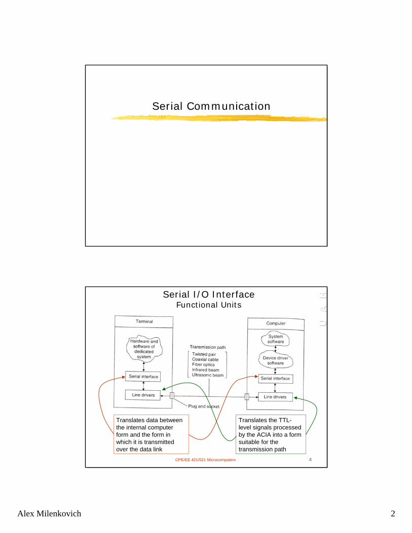
Serial Communication
CPE/EE 421/521 Microcomputers 4
U
A
HU
A
H
U
A
HSerial I/O InterfaceFunctional Units
Translates data between the internal computer form and the form in which it is transmitted over the data link
Translates the TTL-level signals processed by the ACIA into a form suitable for the transmission path
Alex Milenkovich 3
CPE/EE 421/521 Microcomputers 5
U
A
HU
A
H
U
A
H
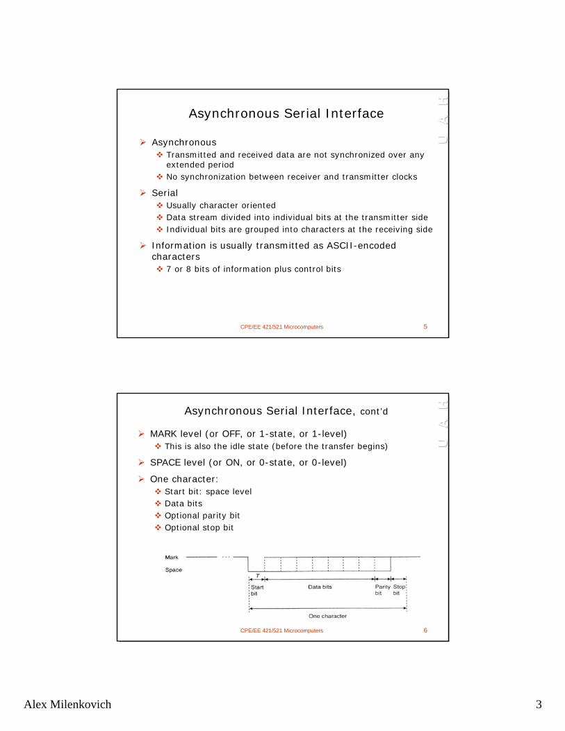
Asynchronous Serial Interface
AsynchronousTransmitted and received data are not synchronized over any extended periodNo synchronization between receiver and transmitter clocks
SerialUsually character orientedData stream divided into individual bits at the transmitter sideIndividual bits are grouped into characters at the receiving side
Information is usually transmitted as ASCII-encoded characters
7 or 8 bits of information plus control bits
CPE/EE 421/521 Microcomputers 6
U
A
HU
A
H
U
A
HAsynchronous Serial Interface, cont’d
MARK level (or OFF, or 1-state, or 1-level)This is also the idle state (before the transfer begins)
SPACE level (or ON, or 0-state, or 0-level)
One character: Start bit: space levelData bitsOptional parity bitOptional stop bit

Alex Milenkovich 4
CPE/EE 421/521 Microcomputers 7
U
A
HU
A
H
U
A
H
12 possible basic formats: 7 or 8 bits of dataOdd, even, or no parity1 or 2 stop bits
Others exist also: no stop bits, 4/5/6 data bits, 1.5 stop bits,etc.
Asynchronous Serial Interface, cont’d
Least significant bit
CPE/EE 421/521 Microcomputers 8
U
A
HU
A
H
U
A
HReceiver Clock Timing
For N=9 bits (7 data + parity + stop) maximum tolerable error is 5%(assume that the receiver clock is slow -- [T + δt] instead of T)
T/2 > (2N+1)δt/2
δt/2 < 1/(2N+1)
δt/T < 100/(2N+1) as a percentage
Alex Milenkovich 5
CPE/EE 421/521 Microcomputers 9
U
A
HU
A
H
U
A
HRS-232 Interface Standard
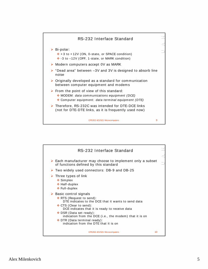
Bi-polar: +3 to +12V (ON, 0-state, or SPACE condition)-3 to –12V (OFF, 1-state, or MARK condition)
Modern computers accept 0V as MARK
“Dead area” between –3V and 3V is designed to absorb line noise
Originally developed as a standard for communication between computer equipment and modems
From the point of view of this standard:MODEM: data communications equipment (DCE)Computer equipment: data terminal equipment (DTE)
Therefore, RS-232C was intended for DTE-DCE links (not for DTE-DTE links, as it is frequently used now)
CPE/EE 421/521 Microcomputers 10
U
A
HU
A
H
U
A
HRS-232 Interface Standard
Each manufacturer may choose to implement only a subset of functions defined by this standard
Two widely used connectors: DB-9 and DB-25
Three types of linkSimplexHalf-duplexFull-duplex
Basic control signalsRTS (Request to send):
DTE indicates to the DCE that it wants to send dataCTS (Clear to send):
DCE indicates that it is ready to receive dataDSR (Data set ready):
indication from the DCE (i.e., the modem) that it is on DTR (Data terminal ready):
indication from the DTE that it is on
Alex Milenkovich 6
CPE/EE 421/521 Microcomputers 11
U
A
HU
A
H
U
A
HRS-232 Interface Standard, another example
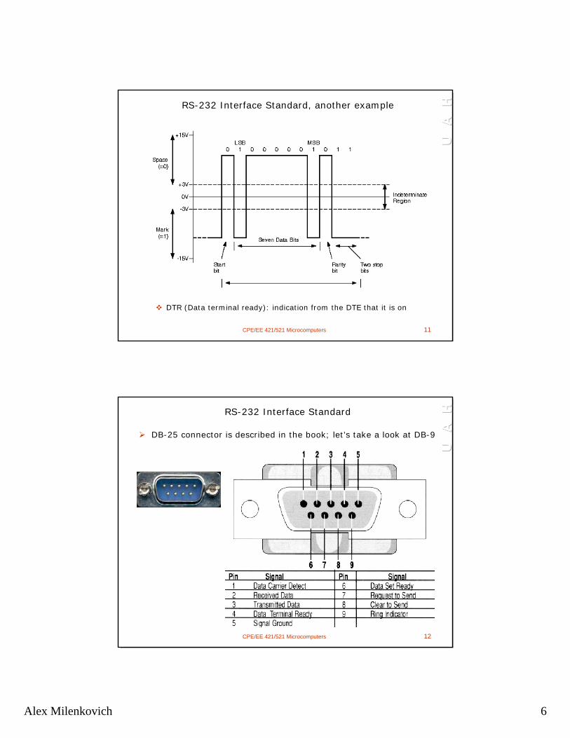
DTR (Data terminal ready): indication from the DTE that it is on
CPE/EE 421/521 Microcomputers 12
U
A
HU
A
H
U
A
HRS-232 Interface Standard
DB-25 connector is described in the book; let’s take a look at DB-9
Alex Milenkovich 7
CPE/EE 421/521 Microcomputers 13
U
A
HU
A
H
U
A
H
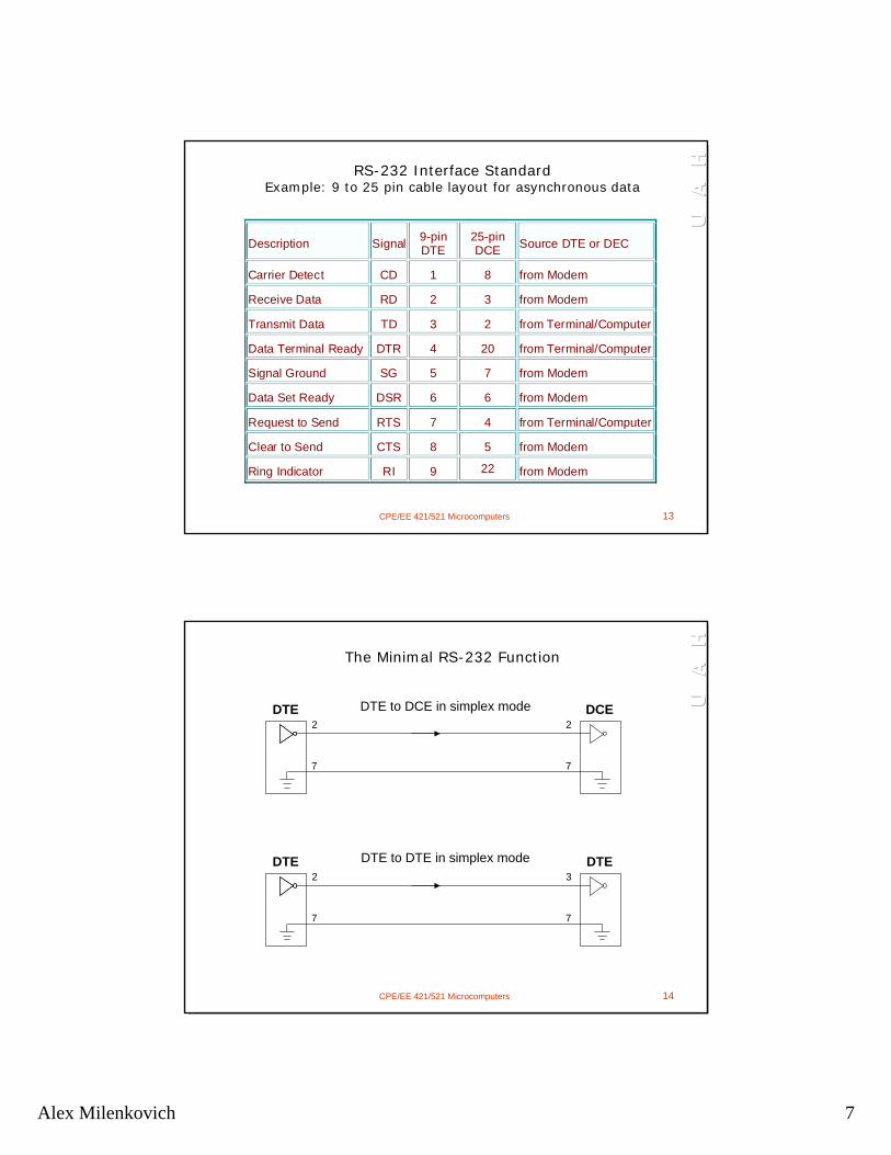
RS-232 Interface StandardExample: 9 to 25 pin cable layout for asynchronous data
Description Signal 9-pin DTE
25-pin DCE Source DTE or DEC
Carrier Detect CD 1 8 from Modem
Receive Data RD 2 3 from Modem
Transmit Data TD 3 2 from Terminal/Computer
Data Terminal Ready DTR 4 20 from Terminal/Computer
Signal Ground SG 5 7 from Modem
Data Set Ready DSR 6 6 from Modem
Request to Send RTS 7 4 from Terminal/Computer
Clear to Send CTS 8 5 from Modem
Ring Indicator RI 9 22 from Modem
CPE/EE 421/521 Microcomputers 14
U
A
HU
A
H
U
A
H
The Minimal RS-232 Function
7
2
7
2DTE DCEDTE to DCE in simplex mode
7
2
7
3DTE DTEDTE to DTE in simplex mode
Alex Milenkovich 8
CPE/EE 421/521 Microcomputers 15
U
A
HU
A
H
U
A
H
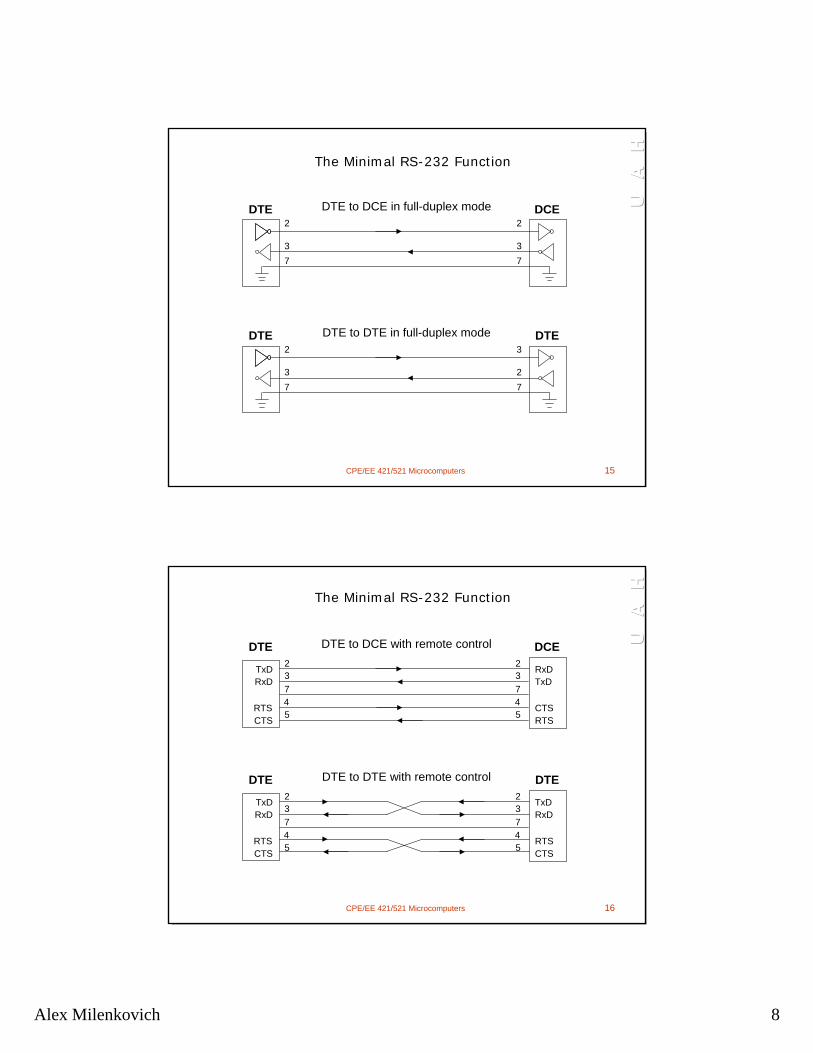
The Minimal RS-232 Function
7
2
7
2DTE DCEDTE to DCE in full-duplex mode
3 3
7
2
7
3DTE DTEDTE to DTE in full-duplex mode
3 2
CPE/EE 421/521 Microcomputers 16
U
A
HU
A
H
U
A
H
The Minimal RS-232 Function
7
2
DTE DCEDTE to DCE with remote control
3
45
TxDRxD
RTSCTS
7
23
45
RxDTxD
CTSRTS
7
2
DTE DTEDTE to DTE with remote control
3
45
TxDRxD
RTSCTS
7
23
45
TxDRxD
RTSCTS
Alex Milenkovich 9
CPE/EE 421/521 Microcomputers 17
U
A
HU
A
H
U
A
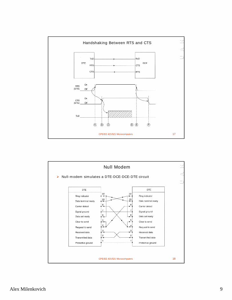
HHandshaking Between RTS and CTS
CPE/EE 421/521 Microcomputers 18
U
A
HU
A
H
U
A
HNull Modem
Null-modem simulates a DTE-DCE-DCE-DTE circuit
Alex Milenkovich 10
CPE/EE 421/521 Microcomputers 19
U
A
HU
A
H
U
A
H
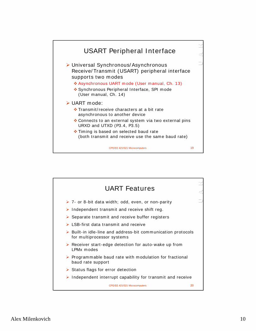
USART Peripheral Interface
Universal Synchronous/Asynchronous Receive/Transmit (USART) peripheral interface supports two modes
Asynchronous UART mode (User manual, Ch. 13)Synchronous Peripheral Interface, SPI mode (User manual, Ch. 14)
UART mode: Transmit/receive characters at a bit rate asynchronous to another deviceConnects to an external system via two external pinsURXD and UTXD (P3.4, P3.5)Timing is based on selected baud rate(both transmit and receive use the same baud rate)
CPE/EE 421/521 Microcomputers 20
U
A
HU
A
H
U
A
H
UART Features
7- or 8-bit data width; odd, even, or non-parity
Independent transmit and receive shift reg.
Separate transmit and receive buffer registers
LSB-first data transmit and receive
Built-in idle-line and address-bit communication protocols for multiprocessor systems
Receiver start-edge detection for auto-wake up from LPMx modes
Programmable baud rate with modulation for fractional baud rate support
Status flags for error detection
Independent interrupt capability for transmit and receive
Alex Milenkovich 11
CPE/EE 421/521 Microcomputers 21
U
A
HU
A
H
U
A
H
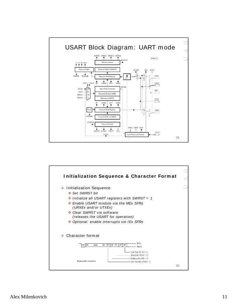
USART Block Diagram: UART mode
CPE/EE 421/521 Microcomputers 22
U
A
HU
A
H
U
A
H
Initialization Sequence & Character Format
Initialization SequenceSet SWRST bitInitialize all USART registers with SWRST = 1Enable USART module via the MEx SFRs (URXEx and/or UTXEx)Clear SWRST via software (releases the USART for operation)Optional: enable interrupts vie IEx SFRs
Character format
Alex Milenkovich 12
CPE/EE 421/521 Microcomputers 23
U
A
HU
A
H
U
A
H
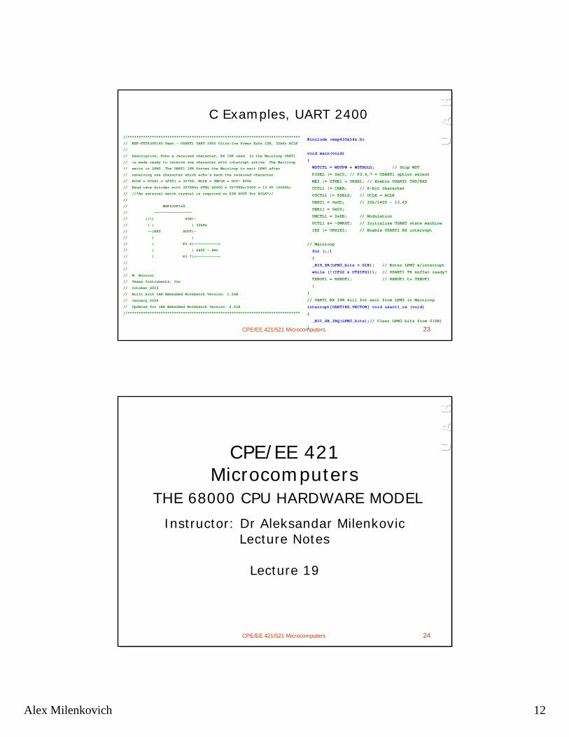
C Examples, UART 2400//******************************************************************************
// MSP-FET430P140 Demo - USART1 UART 2400 Ultra-low Power Echo ISR, 32kHz ACLK
//
// Description; Echo a received character, RX ISR used. In the Mainloop UART1
// is made ready to receive one character with interrupt active. The Mainloop
// waits in LPM3. The UART1 ISR forces the Mainloop to exit LPM3 after
// receiving one character which echo's back the received character.
// ACLK = UCLK1 = LFXT1 = 32768, MCLK = SMCLK = DCO~ 800k
// Baud rate divider with 32768hz XTAL @2400 = 32768Hz/2400 = 13.65 (000Dh)
// //*An external watch crystal is required on XIN XOUT for ACLK*//
//
// MSP430F149
// -----------------
// /|\| XIN|-
// | | | 32kHz
// --|RST XOUT|-
// | |
// | P3.6|----------->
// | | 2400 - 8N1
// | P3.7|<-----------
//
//
// M. Buccini
// Texas Instruments, Inc
// October 2003
// Built with IAR Embedded Workbench Version: 1.26B
// January 2004
// Updated for IAR Embedded Workbench Version: 2.21B
//******************************************************************************
#include <msp430x14x.h>
void main(void)
{
WDTCTL = WDTPW + WDTHOLD; // Stop WDT
P3SEL |= 0xC0; // P3.6,7 = USART1 option select
ME2 |= UTXE1 + URXE1; // Enable USART1 TXD/RXD
UCTL1 |= CHAR; // 8-bit character
UTCTL1 |= SSEL0; // UCLK = ACLK
UBR01 = 0x0D; // 32k/2400 - 13.65
UBR11 = 0x00;
UMCTL1 = 0x6B; // Modulation
UCTL1 &= ~SWRST; // Initialize USART state machine
IE2 |= URXIE1; // Enable USART1 RX interrupt
// Mainloop
for (;;)
{
_BIS_SR(LPM3_bits + GIE); // Enter LPM3 w/interrupt
while (!(IFG2 & UTXIFG1)); // USART1 TX buffer ready?
TXBUF1 = RXBUF1; // RXBUF1 to TXBUF1
}
}
// UART1 RX ISR will for exit from LPM3 in Mainloop
interrupt[UART1RX_VECTOR] void usart1_rx (void)
{
_BIC_SR_IRQ(LPM3_bits);// Clear LPM3 bits from 0(SR)
}
CPE/EE 421/521 Microcomputers 24
U
A
HU
A
H
U
A
HCPE/EE 421
MicrocomputersTHE 68000 CPU HARDWARE MODEL
Instructor: Dr Aleksandar MilenkovicLecture Notes
Lecture 19
Alex Milenkovich 13
CPE/EE 421/521 Microcomputers 25
U
A
HU
A
H
U
A
H
THE 68000 CPU HARDWARE MODELChapter 4
68000 interface
Timing diagram
Minimal configuration using the 68000
CPE/EE 421/521 Microcomputers 26
U
A
HU
A
H
U
A
H68000 Interface
M68000: 64 pins, arranged in 9 groups: Address Bus: A01 – A23
Data Bus: D00 – D15
Asynchronous bus control: AS*, R/W*, UDS*, LDS*,DTACK*, BERR*
Synchronous bus control: E, VPA*, VMA*Bus arbitration control: BR*, BG*, BGACK*Function code: FC0, FC1, FC2System control: CLK, RESET*, HALT*Interrupt control: IPL0*, IPL1*, IPL2*Miscellaneous: Vcc(2), Gnd(2)
Legend: Type• XX Input• XX Output• XX Input/Output
Alex Milenkovich 14
CPE/EE 421/521 Microcomputers 27
U
A
HU
A
H
U
A
H
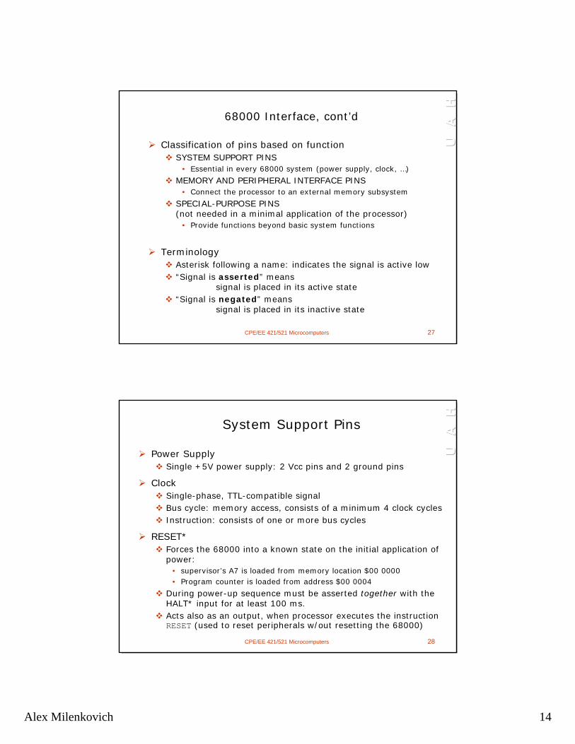
68000 Interface, cont’d
Classification of pins based on functionSYSTEM SUPPORT PINS
• Essential in every 68000 system (power supply, clock, …)
MEMORY AND PERIPHERAL INTERFACE PINS• Connect the processor to an external memory subsystem
SPECIAL-PURPOSE PINS (not needed in a minimal application of the processor)
• Provide functions beyond basic system functions
TerminologyAsterisk following a name: indicates the signal is active low“Signal is asserted” means
signal is placed in its active state“Signal is negated” means
signal is placed in its inactive state
CPE/EE 421/521 Microcomputers 28
U
A
HU
A
H
U
A
H
System Support Pins
Power SupplySingle +5V power supply: 2 Vcc pins and 2 ground pins
ClockSingle-phase, TTL-compatible signalBus cycle: memory access, consists of a minimum 4 clock cyclesInstruction: consists of one or more bus cycles
RESET*Forces the 68000 into a known state on the initial application of power:
• supervisor’s A7 is loaded from memory location $00 0000• Program counter is loaded from address $00 0004
During power-up sequence must be asserted together with the HALT* input for at least 100 ms. Acts also as an output, when processor executes the instruction RESET (used to reset peripherals w/out resetting the 68000)
Alex Milenkovich 15
CPE/EE 421/521 Microcomputers 29
U
A
HU
A
H
U
A
H
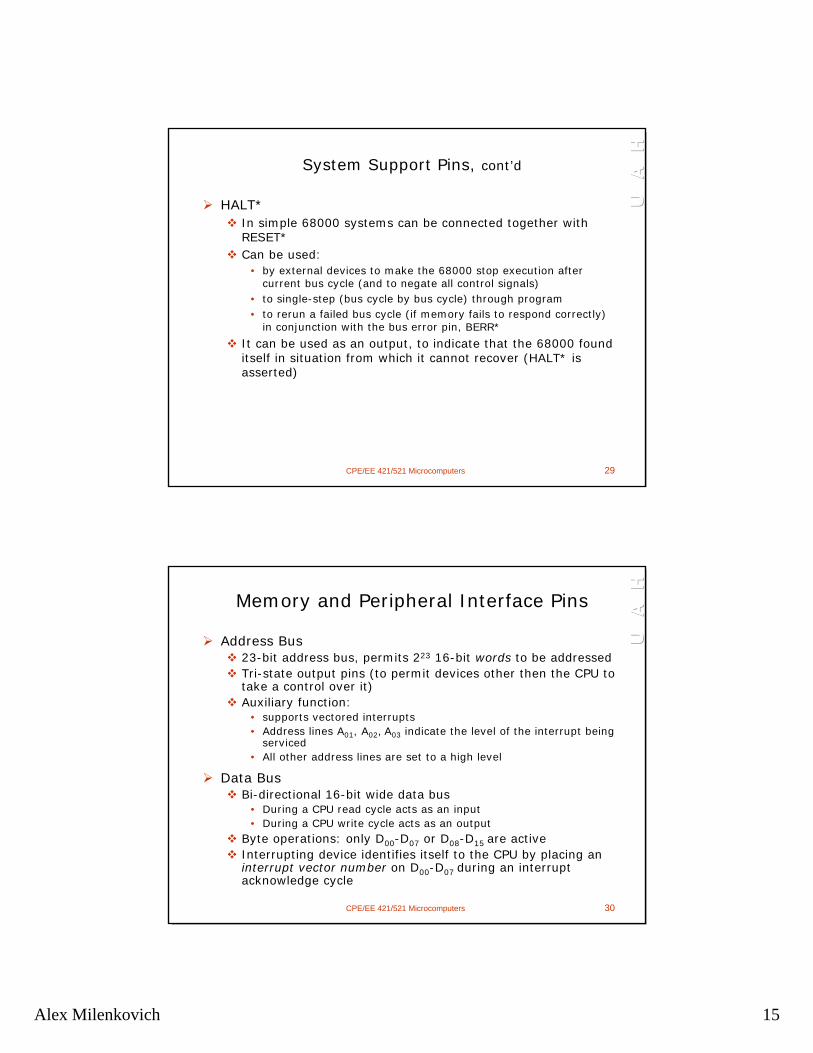
System Support Pins, cont’d
HALT*In simple 68000 systems can be connected together with RESET*Can be used:
• by external devices to make the 68000 stop execution after current bus cycle (and to negate all control signals)
• to single-step (bus cycle by bus cycle) through program • to rerun a failed bus cycle (if memory fails to respond correctly)
in conjunction with the bus error pin, BERR*
It can be used as an output, to indicate that the 68000 found itself in situation from which it cannot recover (HALT* is asserted)
CPE/EE 421/521 Microcomputers 30
U
A
HU
A
H
U
A
H
Memory and Peripheral Interface Pins
Address Bus23-bit address bus, permits 223 16-bit words to be addressedTri-state output pins (to permit devices other then the CPU to take a control over it)Auxiliary function:
• supports vectored interrupts• Address lines A01, A02, A03 indicate the level of the interrupt being
serviced• All other address lines are set to a high level
Data BusBi-directional 16-bit wide data bus
• During a CPU read cycle acts as an input• During a CPU write cycle acts as an output
Byte operations: only D00-D07 or D08-D15 are activeInterrupting device identifies itself to the CPU by placing an interrupt vector number on D00-D07 during an interrupt acknowledge cycle
Alex Milenkovich 16
CPE/EE 421/521 Microcomputers 31
U
A
HU
A
H
U
A
H
Memory and Peripheral Interface Pins, cont’d
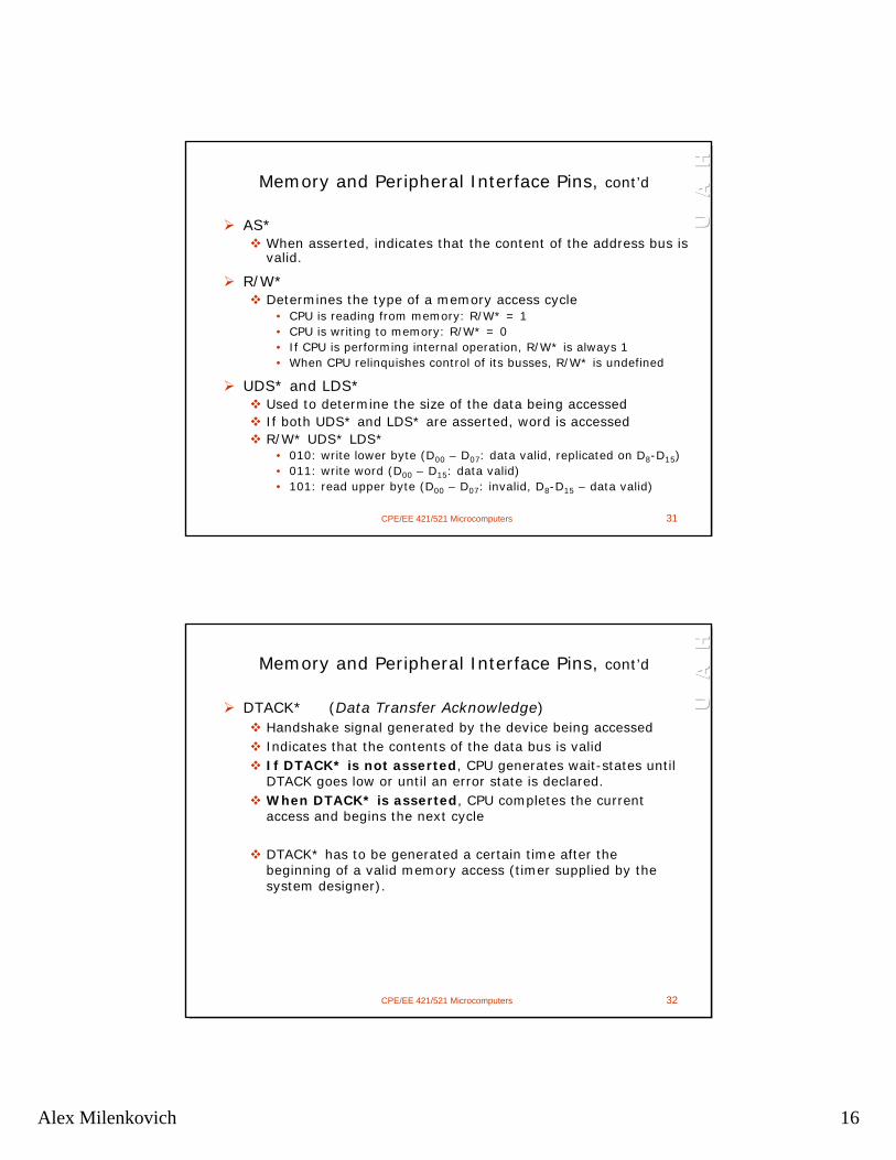
AS*When asserted, indicates that the content of the address bus is valid.
R/W*Determines the type of a memory access cycle
• CPU is reading from memory: R/W* = 1• CPU is writing to memory: R/W* = 0• If CPU is performing internal operation, R/W* is always 1• When CPU relinquishes control of its busses, R/W* is undefined
UDS* and LDS*Used to determine the size of the data being accessedIf both UDS* and LDS* are asserted, word is accessedR/W* UDS* LDS*
• 010: write lower byte (D00 – D07: data valid, replicated on D8-D15)• 011: write word (D00 – D15: data valid)• 101: read upper byte (D00 – D07: invalid, D8-D15 – data valid)
CPE/EE 421/521 Microcomputers 32
U
A
HU
A
H
U
A
H
Memory and Peripheral Interface Pins, cont’d
DTACK* (Data Transfer Acknowledge)Handshake signal generated by the device being accessedIndicates that the contents of the data bus is validIf DTACK* is not asserted, CPU generates wait-states until DTACK goes low or until an error state is declared. When DTACK* is asserted, CPU completes the current access and begins the next cycle
DTACK* has to be generated a certain time after the beginning of a valid memory access (timer supplied by the system designer).

Alex Milenkovich 17
CPE/EE 421/521 Microcomputers 33
U
A
HU
A
H
U
A
H
Memory and Peripheral Interface Pins, cont’d
Figure 4.3
CPE/EE 421/521 Microcomputers 34
U
A
HU
A
H
U
A
H
Special-Function Pins of the 68000
BERR* (Bus Error Control)Enables the 68000 to recover from errors within the memory system
BR*, BG*, BGACK* (Bus Arbitration Control)Used to implement multiprocessor systems based on M68000
FC0-FC2 (Function Code Output)Indicate the type of cycle currently being executedBecomes valid approximately half a clock cycle earlier than the contents of the address bus
IPL0*-IPL2* (Interrupt Control Interface)Used by an external device to indicate that it requires service3-bit code specifies one of eight levels of interrupt request
Alex Milenkovich 18
CPE/EE 421/521 Microcomputers 35
U
A
HU
A
H
U
A
H
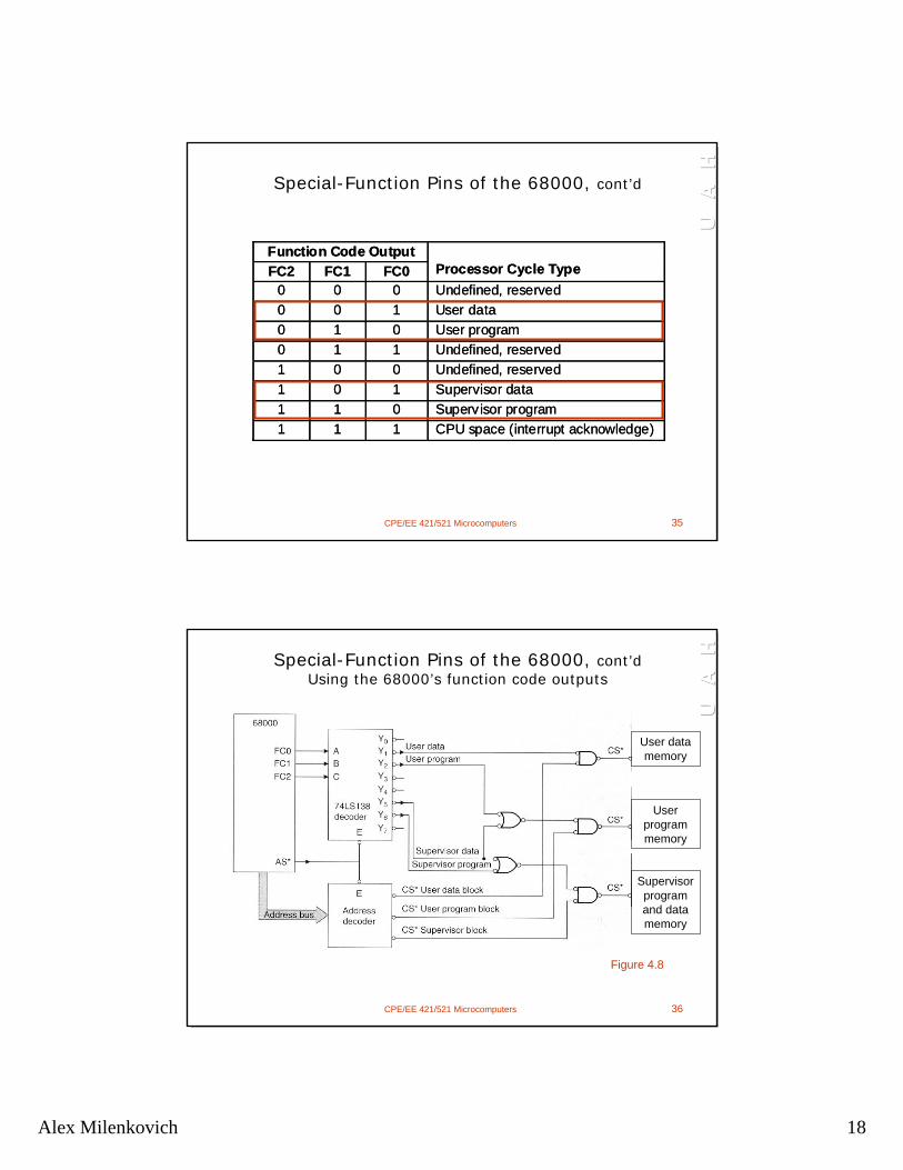
Special-Function Pins of the 68000, cont’d
Function Code Output FC2 FC1 FC0 Processor Cycle Type
0 0 0 Undefined, reserved 0 0 1 User data 0 1 0 User program 0 1 1 Undefined, reserved 1 0 0 Undefined, reserved 1 0 1 Supervisor data 1 1 0 Supervisor program 1 1 1 CPU space (interrupt acknowledge)
Function Code Output FC2 FC1 FC0 Processor Cycle Type
0 0 0 Undefined, reserved 0 0 1 User data 0 1 0 User program 0 1 1 Undefined, reserved 1 0 0 Undefined, reserved 1 0 1 Supervisor data 1 1 0 Supervisor program 1 1 1 CPU space (interrupt acknowledge)
CPE/EE 421/521 Microcomputers 36
U
A
HU
A
H
U
A
H
Special-Function Pins of the 68000, cont’dUsing the 68000’s function code outputs
User data memory
User program memory
Supervisor program and data memory
Figure 4.8

Alex Milenkovich 19
CPE/EE 421/521 Microcomputers 37
U
A
HU
A
H
U
A
HSpecial-Function Pins of the 68000, cont’dAsynchronous Bus Control
The 68000 is not fully asynchronous because its actions are synchronized with a clock input
It can prolong a memory access until an ACK is received, but it has to be in increments of one clock cycle
Figure 4.11
CPE/EE 421/521 Microcomputers 38
U
A
HU
A
H
U
A
H
Interpreting the Timing Diagram
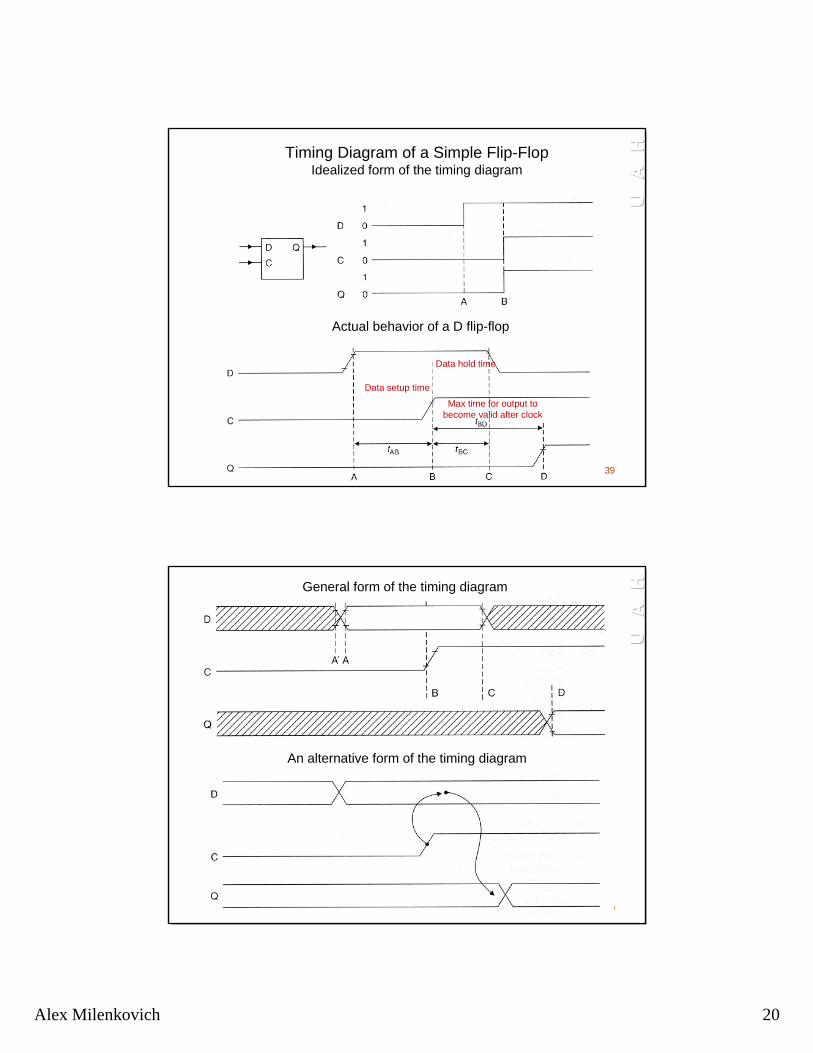
Alex Milenkovich 20
CPE/EE 421/521 Microcomputers 39
U
A
HU
A
H
U
A
H
Actual behavior of a D flip-flop
Timing Diagram of a Simple Flip-FlopIdealized form of the timing diagram
Data hold time
Data setup time
Max time for output to become valid after clock
CPE/EE 421/521 Microcomputers 40
U
A
HU
A
H
U
A
H
An alternative form of the timing diagram
General form of the timing diagram
Alex Milenkovich 21
CPE/EE 421/521 Microcomputers 41
U
A
HU
A
H
U
A
H
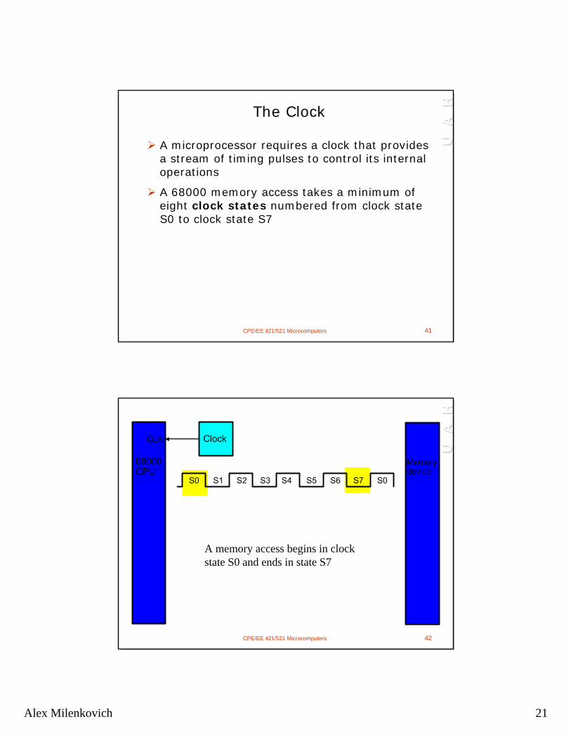
The Clock
A microprocessor requires a clock that provides a stream of timing pulses to control its internal operations
A 68000 memory access takes a minimum of eight clock states numbered from clock state S0 to clock state S7
CPE/EE 421/521 Microcomputers 42
U
A
HU
A
H
U
A
H
A memory access begins in clockstate S0 and ends in state S7

Alex Milenkovich 22
CPE/EE 421/521 Microcomputers 43
U
A
HU
A
H
U
A
H
The most important parameterof the clock is the duration of a cycle,tCYC.
CPE/EE 421/521 Microcomputers 44
U
A
HU
A
H
U
A
H
At the start of a memory accessthe CPU sends the address of the locationit wishes to read to the memory

Alex Milenkovich 23
CPE/EE 421/521 Microcomputers 45
U
A
HU
A
H
U
A
H
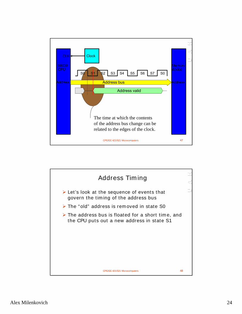
Address Timing
We are interested in when the 68000 generates a new address for use in the current memory access
The next slide shows the relationship between the new address and the state of the 68000’s clock
CPE/EE 421/521 Microcomputers 46
U
A
HU
A
H
U
A
H
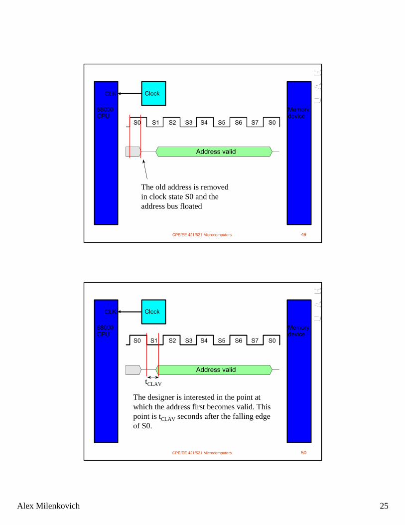
Initially, in stateS0 the addressbus contains theold address
In state S1 a newaddress becomesvalid for the remainderof the memory access
Alex Milenkovich 24
CPE/EE 421/521 Microcomputers 47
U
A
HU
A
H
U
A
H
The time at which the contentsof the address bus change can berelated to the edges of the clock.
CPE/EE 421/521 Microcomputers 48
U
A
HU
A
H
U
A
H
Address Timing
Let’s look at the sequence of events that govern the timing of the address bus
The “old” address is removed in state S0
The address bus is floated for a short time, and the CPU puts out a new address in state S1
Alex Milenkovich 25
CPE/EE 421/521 Microcomputers 49
U
A
HU
A
H
U
A
H
The old address is removedin clock state S0 and theaddress bus floated
CPE/EE 421/521 Microcomputers 50
U
A
HU
A
H
U
A
H
tCLAV
The designer is interested in the point atwhich the address first becomes valid. Thispoint is tCLAV seconds after the falling edgeof S0.
Alex Milenkovich 26
CPE/EE 421/521 Microcomputers 51
U
A
HU
A
H
U
A
H
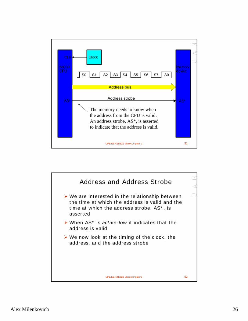
The memory needs to know whenthe address from the CPU is valid.An address strobe, AS*, is assertedto indicate that the address is valid.
CPE/EE 421/521 Microcomputers 52
U
A
HU
A
H
U
A
H
Address and Address Strobe
We are interested in the relationship between the time at which the address is valid and the time at which the address strobe, AS*, is asserted
When AS* is active-low it indicates that the address is valid
We now look at the timing of the clock, the address, and the address strobe
Alex Milenkovich 27
CPE/EE 421/521 Microcomputers 53
U
A
HU
A
H
U
A
H
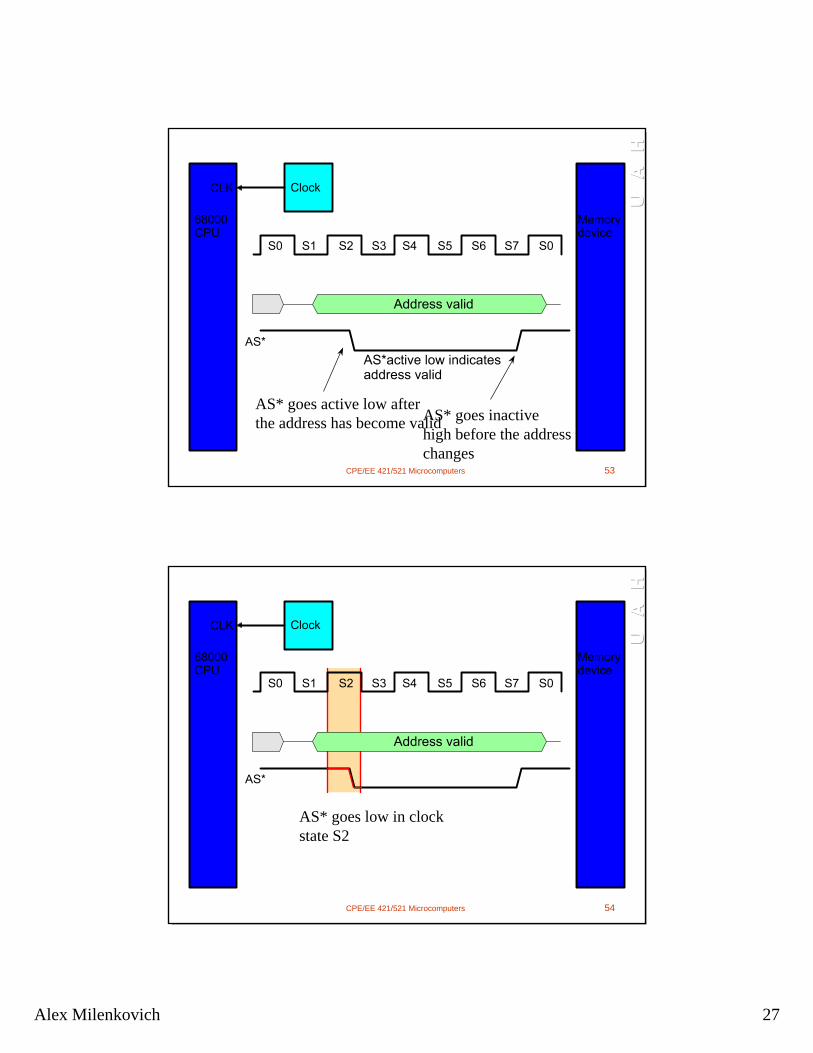
AS* goes active low afterthe address has become validAS* goes inactive
high before the addresschanges
CPE/EE 421/521 Microcomputers 54
U
A
HU
A
H
U
A
H
AS* goes low in clockstate S2
Alex Milenkovich 28
CPE/EE 421/521 Microcomputers 55
U
A
HU
A
H
U
A
H
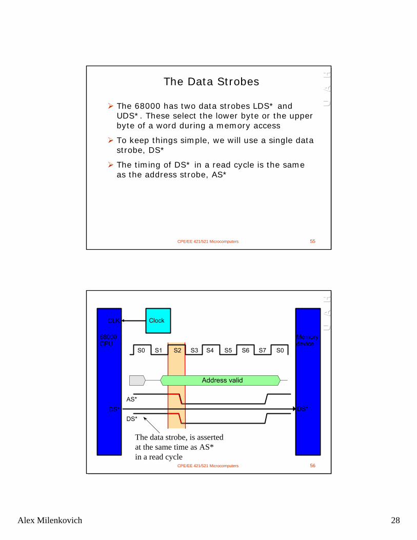
The Data Strobes
The 68000 has two data strobes LDS* and UDS*. These select the lower byte or the upper byte of a word during a memory access
To keep things simple, we will use a single data strobe, DS*
The timing of DS* in a read cycle is the same as the address strobe, AS*
CPE/EE 421/521 Microcomputers 56
U
A
HU
A
H
U
A
H
The data strobe, is assertedat the same time as AS*in a read cycle
Alex Milenkovich 29
CPE/EE 421/521 Microcomputers 57
U
A
HU
A
H
U
A
H
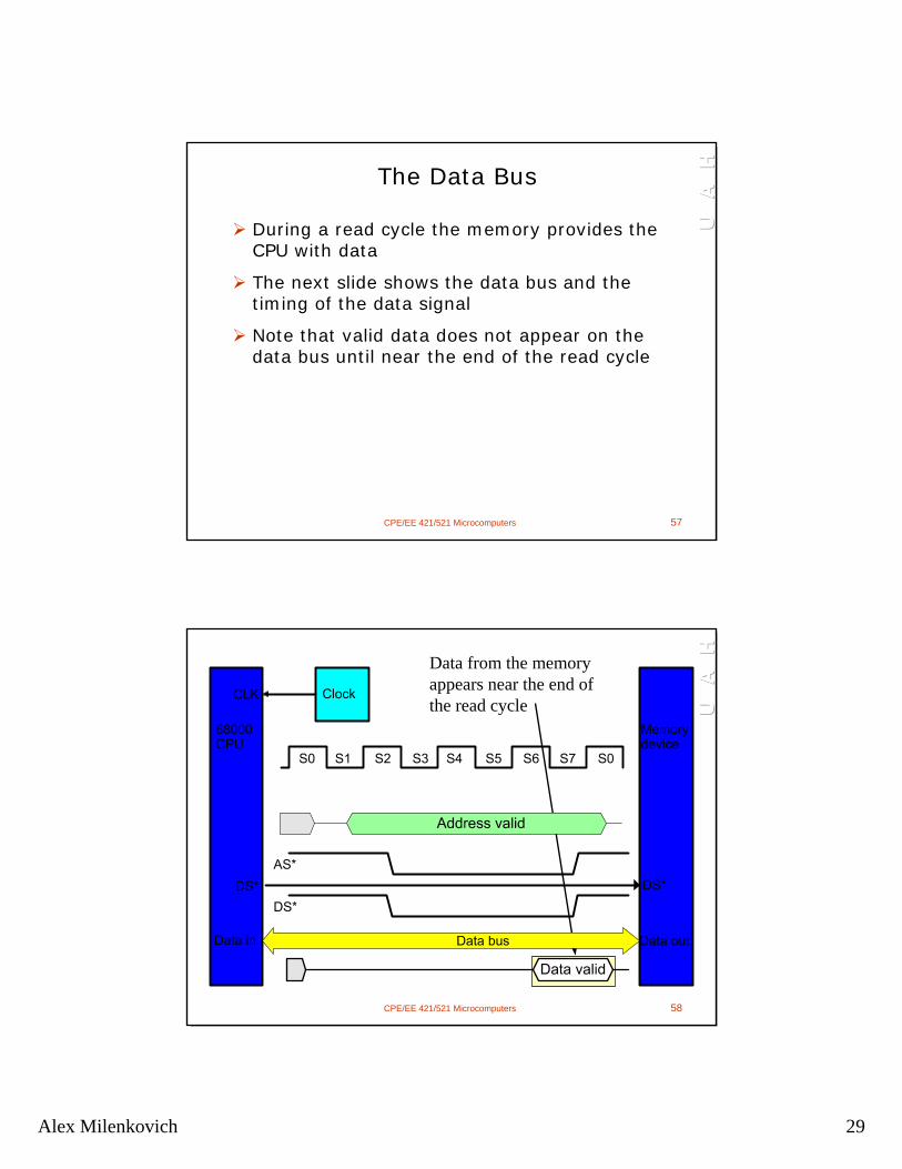
The Data Bus
During a read cycle the memory provides the CPU with data
The next slide shows the data bus and the timing of the data signal
Note that valid data does not appear on the data bus until near the end of the read cycle
CPE/EE 421/521 Microcomputers 58
U
A
HU
A
H
U
A
H
Data from the memoryappears near the end ofthe read cycle

Alex Milenkovich 30
CPE/EE 421/521 Microcomputers 59
U
A
HU
A
H
U
A
H
Analyzing the Timing Diagram
We are going to redraw the timing diagram to remove clutter
We aren’t interested in the signal paths themselves, only in the relationship between the signals
CPE/EE 421/521 Microcomputers 60
U
A
HU
A
H
U
A
H
We are interested in the relationshipbetween the clock, AS*/DS* andthe data in a read cycle
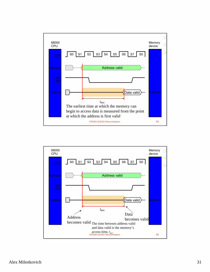
Alex Milenkovich 31
CPE/EE 421/521 Microcomputers 61
U
A
HU
A
H
U
A
H
The earliest time at which the memory canbegin to access data is measured from the pointat which the address is first valid
CPE/EE 421/521 Microcomputers 62
U
A
HU
A
H
U
A
H
Addressbecomes valid
Databecomes valid
The time between address validand data valid is the memory’saccess time, tacc
Alex Milenkovich 32
CPE/EE 421/521 Microcomputers 63
U
A
HU
A
H
U
A
H
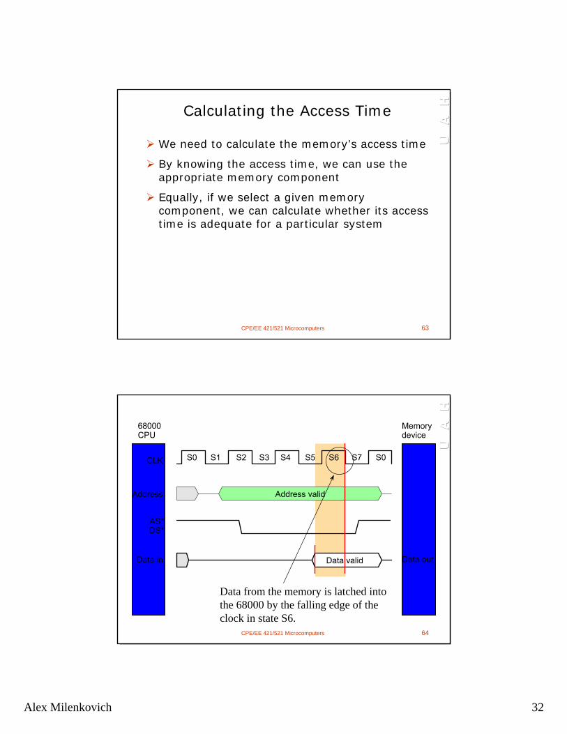
Calculating the Access Time
We need to calculate the memory’s access time
By knowing the access time, we can use the appropriate memory component
Equally, if we select a given memory component, we can calculate whether its access time is adequate for a particular system
CPE/EE 421/521 Microcomputers 64
U
A
HU
A
H
U
A
H
Data from the memory is latched intothe 68000 by the falling edge of theclock in state S6.
Alex Milenkovich 33
CPE/EE 421/521 Microcomputers 65
U
A
HU
A
H
U
A
H
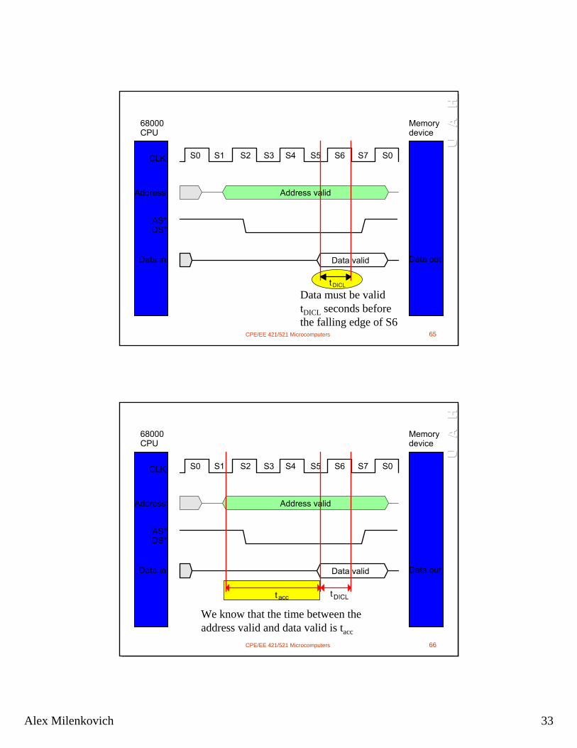
Data must be validtDICL seconds beforethe falling edge of S6
CPE/EE 421/521 Microcomputers 66
U
A
HU
A
H
U
A
H
We know that the time between theaddress valid and data valid is tacc
Alex Milenkovich 34
CPE/EE 421/521 Microcomputers 67
U
A
HU
A
H
U
A
H
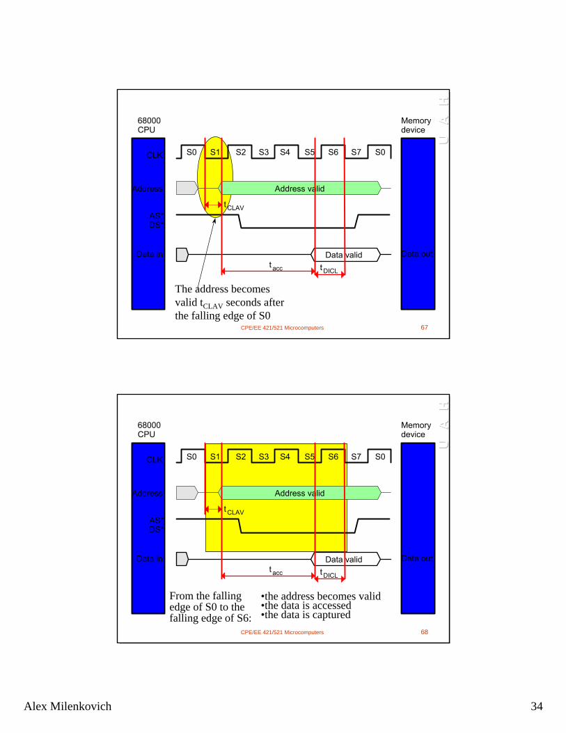
The address becomesvalid tCLAV seconds afterthe falling edge of S0
CPE/EE 421/521 Microcomputers 68
U
A
HU
A
H
U
A
H
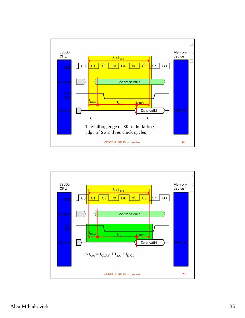
From the fallingedge of S0 to thefalling edge of S6:
•the address becomes valid•the data is accessed•the data is captured
Alex Milenkovich 35
CPE/EE 421/521 Microcomputers 69
U
A
HU
A
H
U
A
H
The falling edge of S0 to the fallingedge of S6 is three clock cycles
CPE/EE 421/521 Microcomputers 70
U
A
HU
A
H
U
A
H
3 tcyc = tCLAV + tacc + tDICL
Alex Milenkovich 36
CPE/EE 421/521 Microcomputers 71
U
A
HU
A
H
U
A
H
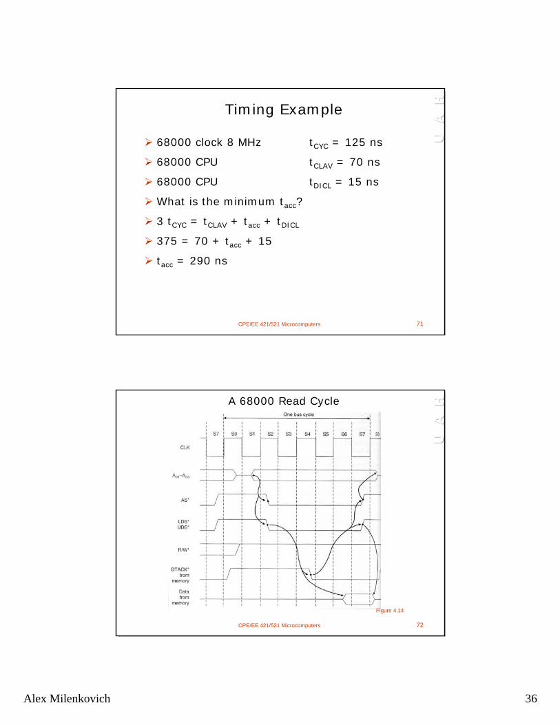
Timing Example
68000 clock 8 MHz tCYC = 125 ns
68000 CPU tCLAV = 70 ns
68000 CPU tDICL = 15 ns
What is the minimum tacc?
3 tCYC = tCLAV + tacc + tDICL
375 = 70 + tacc + 15
tacc = 290 ns
CPE/EE 421/521 Microcomputers 72
U
A
HU
A
H
U
A
H
Figure 4.14
A 68000 Read Cycle
Alex Milenkovich 37
CPE/EE 421/521 Microcomputers 73
U
A
HU
A
H
U
A
H
Figure 4.15
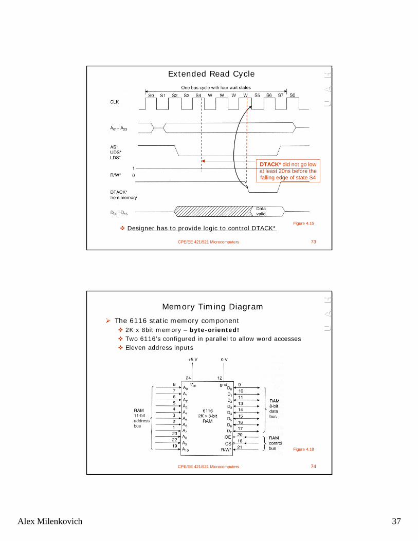
Extended Read Cycle
DTACK* did not go low at least 20ns before the falling edge of state S4
Designer has to provide logic to control DTACK*
CPE/EE 421/521 Microcomputers 74
U
A
HU
A
H
U
A
H
Figure 4.18
Memory Timing Diagram
The 6116 static memory component2K x 8bit memory – byte-oriented!Two 6116’s configured in parallel to allow word accessesEleven address inputs
Alex Milenkovich 38
CPE/EE 421/521 Microcomputers 75
U
A
HU
A
H
U
A
H
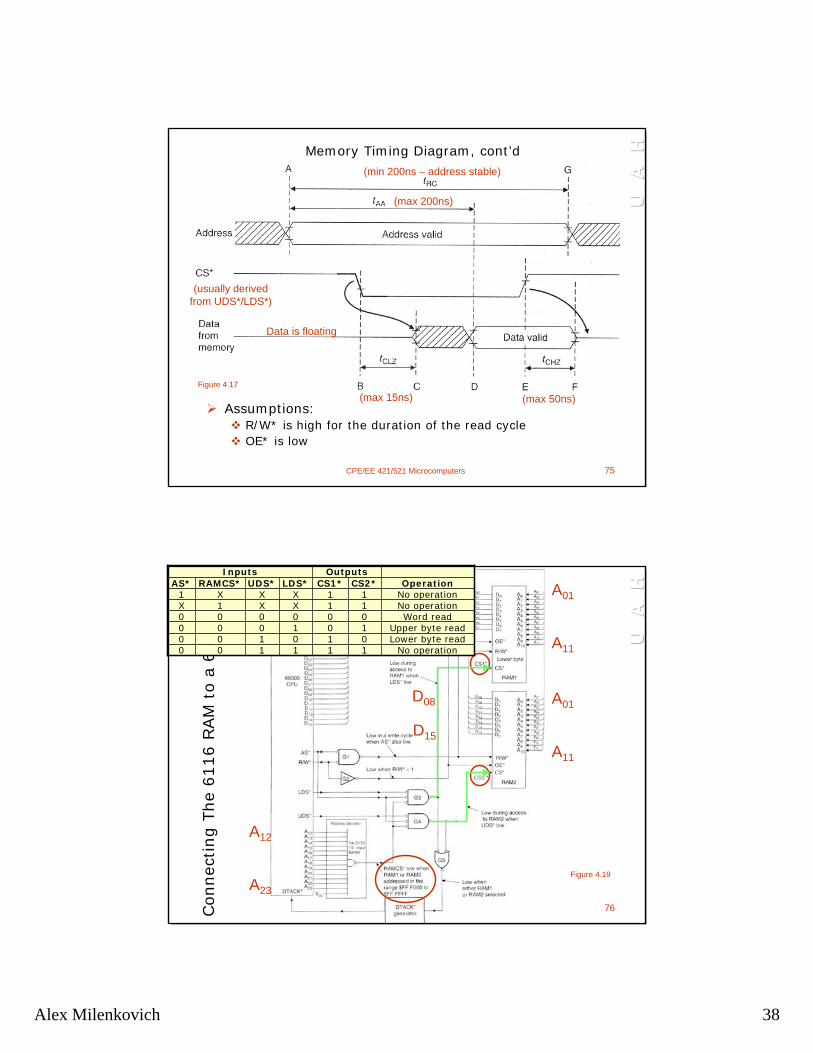
Figure 4.17
Assumptions:R/W* is high for the duration of the read cycleOE* is low
Memory Timing Diagram, cont’d(min 200ns – address stable)
(max 200ns)
(max 15ns)
Data is floating
(max 50ns)
(usually derived from UDS*/LDS*)
CPE/EE 421/521 Microcomputers 76
U
A
HU
A
H
U
A
HD00
D07
D08
D15
A12
A23
A01
A11
A01
A11
A01
A11
Figure 4.19
Connec
ting T
he
6116 R
AM
to a
68000 C
PU
No operation111100Lower byte read010100Upper byte read101000
Word read000000No operation11XX1XNo operation11XXX1OperationCS2*CS1*LDS*UDS*RAMCS*AS*
OutputsInputs
Alex Milenkovich 39
CPE/EE 421/521 Microcomputers 77
U
A
HU
A
H
U
A
H
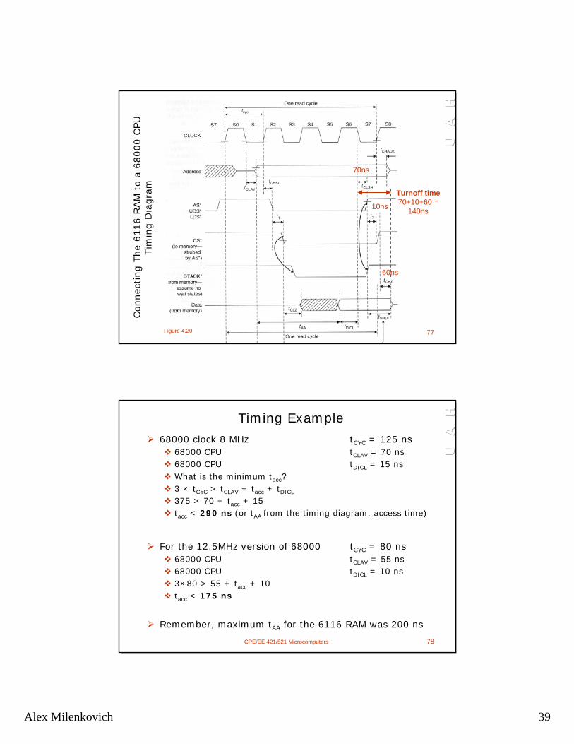
Figure 4.20
Connec
ting T
he
6116 R
AM
to
a 68000 C
PUTim
ing D
iagra
m
Turnoff time70+10+60 =
140ns
70ns
10ns
60ns
CPE/EE 421/521 Microcomputers 78
U
A
HU
A
H
U
A
HTiming Example
68000 clock 8 MHz tCYC = 125 ns68000 CPU tCLAV = 70 ns68000 CPU tDICL = 15 nsWhat is the minimum tacc?3 × tCYC > tCLAV + tacc + tDICL
375 > 70 + tacc + 15tacc < 290 ns (or tAA from the timing diagram, access time)
For the 12.5MHz version of 68000 tCYC = 80 ns68000 CPU tCLAV = 55 ns68000 CPU tDICL = 10 ns3×80 > 55 + tacc + 10tacc < 175 ns
Remember, maximum tAA for the 6116 RAM was 200 ns
Alex Milenkovich 40
CPE/EE 421/521 Microcomputers 79
U
A
HU
A
H
U
A
H
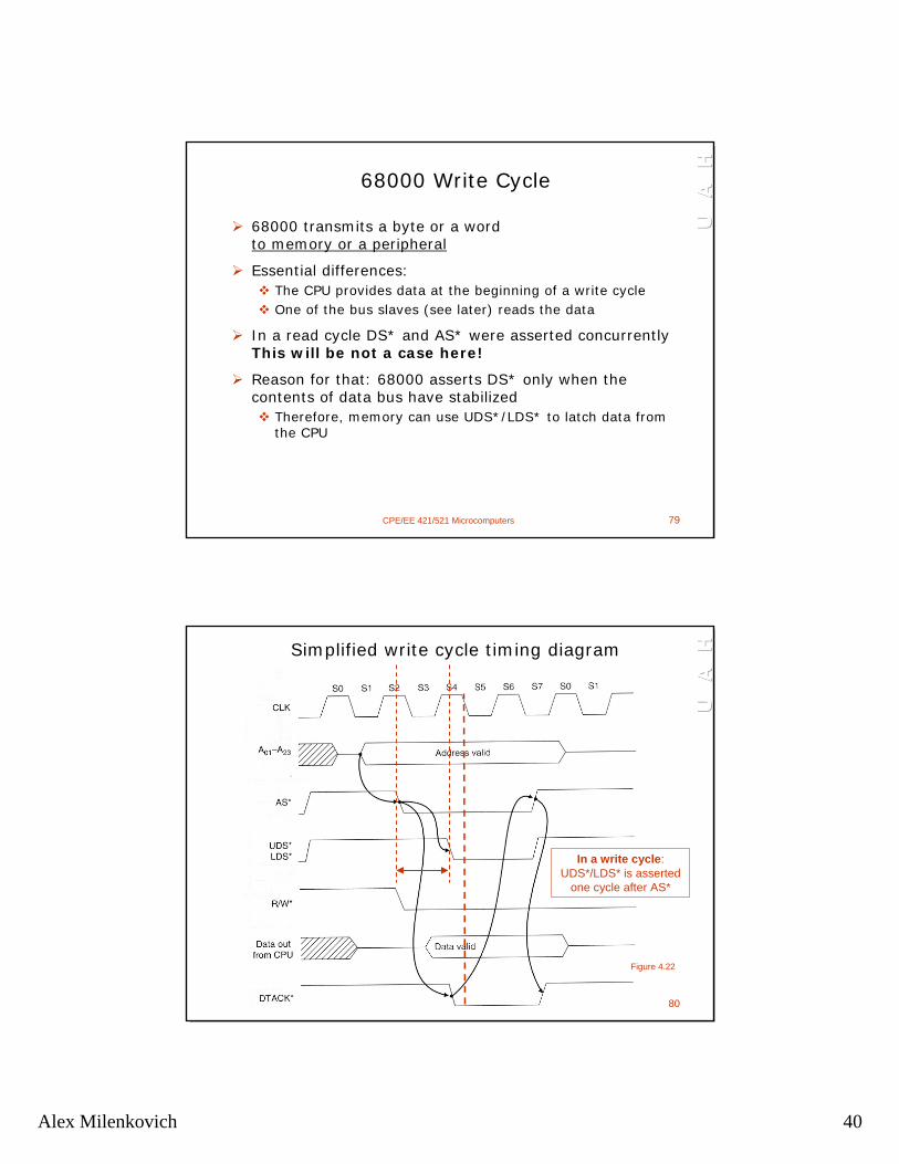
68000 Write Cycle
68000 transmits a byte or a word to memory or a peripheral
Essential differences:The CPU provides data at the beginning of a write cycleOne of the bus slaves (see later) reads the data
In a read cycle DS* and AS* were asserted concurrentlyThis will be not a case here!
Reason for that: 68000 asserts DS* only when the contents of data bus have stabilized
Therefore, memory can use UDS*/LDS* to latch data from the CPU
CPE/EE 421/521 Microcomputers 80
U
A
HU
A
H
U
A
HSimplified write cycle timing diagram
In a write cycle: UDS*/LDS* is asserted
one cycle after AS*
Figure 4.22
Alex Milenkovich 41
CPE/EE 421/521 Microcomputers 81
U
A
HU
A
H
U
A
H
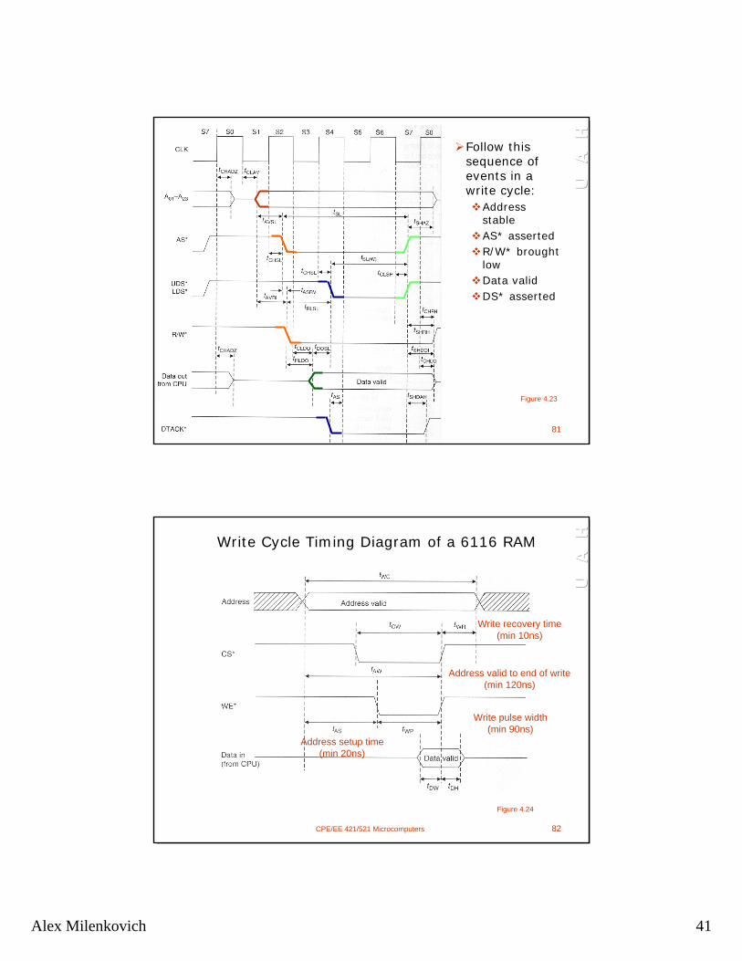
Figure 4.23
Follow this sequence of events in a write cycle:
Address stableAS* assertedR/W* brought lowData validDS* asserted
CPE/EE 421/521 Microcomputers 82
U
A
HU
A
H
U
A
H
Figure 4.24
Write Cycle Timing Diagram of a 6116 RAM
Address setup time(min 20ns)
Address valid to end of write(min 120ns)
Write pulse width(min 90ns)
Write recovery time(min 10ns)
Alex Milenkovich 42
CPE/EE 421/521 Microcomputers 83
U
A
HU
A
H
U
A
H
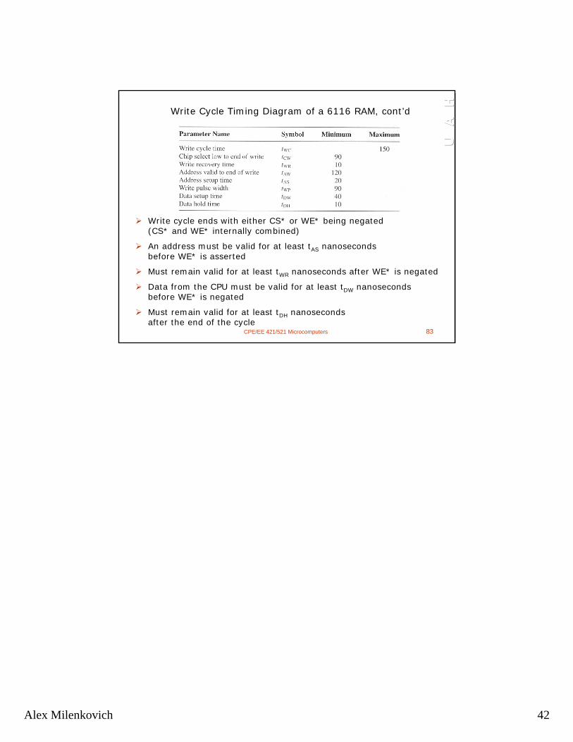
Write Cycle Timing Diagram of a 6116 RAM, cont’d
Write cycle ends with either CS* or WE* being negated (CS* and WE* internally combined)
An address must be valid for at least tAS nanoseconds before WE* is asserted
Must remain valid for at least tWR nanoseconds after WE* is negated
Data from the CPU must be valid for at least tDW nanoseconds before WE* is negated
Must remain valid for at least tDH nanoseconds after the end of the cycle