Cost effective test methodology using pmu for automated test equipment systems
13
International Journal of VLSI design & Communication Systems (VLSICS) Vol.5, No.1, February 2014 DOI : 10.5121/vlsic.2014.5102 15 COST EFFECTIVE TEST METHODOLOGY USING PMU FOR AUTOMATED TEST EQUIPMENT SYSTEMS In-Seok Jung 1 , Yong-Bin Kim 1 and Kyung Ki Kim 2** 1 Department of Electrical and Computer Engineering, Northeastern University, Boston, MA, USA 2 Department of Electronic Engineering, Daegu University, Gyeongsan, South Korea ABSTRACT In this paper, test methodology using parametric measurement unit is proposed for Automated Test Equipment (ATE) systems using 600MHz Driver, Comparator, and Active load (DCL). ATE systems is a very important means to reduce the device test cost, and the systems should be able to test several modes to check the performance characteristics of the device. The proposed methodology provides four different types of test operation for DC and AC analysis of the Device-Under-Test(DUT). Along with the proposed methodology, the paper proposes ATE system integration methodology for cost effective ATE integration for high speed test. The measured test results using the proposed method and system turned out to be well within the target specifications with high accuracies. KEYWORDS Automated Test Equipment, ATE, DCL, Pin Parametric Unit, Test Methodology 1. INTRODUCTION Automatic test equipment (ATE) systems play a key role in the manufacture of semiconductor devices including BJT and CMOS devices. More commonly called “testers”, the equipment allows manufacturers to test each device for engineering characterization and/or production validation. It is critical to guarantee every chip’s correct operation with an acceptable performance in the field for the continued success of the semiconductor device manufacturer. Unfortunately, it is possible to guarantee the correct function with an acceptable performance only after a costly test. In general, the test cost increases with the complexity of the device-under- test (DUT). Cost of test is one of the most important factors in deciding the type of tester. That is one of the reasons why cost effective ATE systems should be developed [1]. Much of the cost of a semiconductor tester is wrapped into the channel architecture. A channel may be thought of as the electronic resources in the tester that interface with one pin of the device-under-test (DUT). If the DUT pins require high performance and high accuracy test signals in order to adequately test the part, each channel may require a host of costly enabling features to achieve the performance. On the other hand, a channel architecture may be greatly simplified, and less costly, if the performance parameters are low [2]. _______________________________ **Corresponding author (Kyung Ki Kim)
-
Upload
vlsics -
Category
Technology
-
view
417 -
download
1
description
In this paper, test methodology using parametric measurement unit is proposed for Automated Test Equipment (ATE) systems using 600MHz Driver, Comparator, and Active load (DCL). ATE systems is a very important means to reduce the device test cost, and the systems should be able to test several modes to check the performance characteristics of the device. The proposed methodology provides four different types of test operation for DC and AC analysis of the Device-Under-Test(DUT). Along with the proposed methodology, the paper proposes ATE system integration methodology for cost effective ATE integration for high speed test. The measured test results using the proposed method and system turned out to be well within the target specifications with high accuracies
Transcript of Cost effective test methodology using pmu for automated test equipment systems

International Journal of VLSI design & Communication Systems (VLSICS) Vol.5, No.1, February 2014
DOI : 10.5121/vlsic.2014.5102 15
COST EFFECTIVE TEST METHODOLOGY
USING PMU FOR AUTOMATED TEST
EQUIPMENT SYSTEMS
In-Seok Jung1, Yong-Bin Kim
1 and Kyung Ki Kim
2**
1Department of Electrical and Computer Engineering,
Northeastern University, Boston, MA, USA 2Department of Electronic Engineering, Daegu University, Gyeongsan, South Korea
ABSTRACT
In this paper, test methodology using parametric measurement unit is proposed for Automated Test
Equipment (ATE) systems using 600MHz Driver, Comparator, and Active load (DCL). ATE systems is a
very important means to reduce the device test cost, and the systems should be able to test several modes to
check the performance characteristics of the device. The proposed methodology provides four different
types of test operation for DC and AC analysis of the Device-Under-Test(DUT). Along with the proposed
methodology, the paper proposes ATE system integration methodology for cost effective ATE integration
for high speed test. The measured test results using the proposed method and system turned out to be well
within the target specifications with high accuracies.
KEYWORDS
Automated Test Equipment, ATE, DCL, Pin Parametric Unit, Test Methodology
1. INTRODUCTION
Automatic test equipment (ATE) systems play a key role in the manufacture of semiconductor
devices including BJT and CMOS devices. More commonly called “testers”, the equipment
allows manufacturers to test each device for engineering characterization and/or production
validation. It is critical to guarantee every chip’s correct operation with an acceptable
performance in the field for the continued success of the semiconductor device manufacturer.
Unfortunately, it is possible to guarantee the correct function with an acceptable performance
only after a costly test. In general, the test cost increases with the complexity of the device-under-
test (DUT). Cost of test is one of the most important factors in deciding the type of tester. That is
one of the reasons why cost effective ATE systems should be developed [1].
Much of the cost of a semiconductor tester is wrapped into the channel architecture. A channel
may be thought of as the electronic resources in the tester that interface with one pin of the
device-under-test (DUT). If the DUT pins require high performance and high accuracy test
signals in order to adequately test the part, each channel may require a host of costly enabling
features to achieve the performance. On the other hand, a channel architecture may be greatly
simplified, and less costly, if the performance parameters are low [2].
_______________________________
**Corresponding author (Kyung Ki Kim)

International Journal of VLSI design & Communication Systems (VLSICS) Vol.5, No.1, February 2014
16
Typically, as shown in Figure 1, the conventional channel architecture for a semiconductor tester
includes AC test circuitry in the form of an AC driver in response to a pattern generator and DC
test circuitry including a DC parametric measurement unit. Generally, the AC driver generates
and drives AC test waveforms along a transmission line to a DUT, while the DC test circuitry
forces a DC voltage or current to the DUT and performs various DC measurements. Usually, AC
and DC tests are performed on the tester at separate times. The AC driver circuitry couples to the
DUT via the transmission line with a complementary comparator circuit. The comparator circuit
captures signals from the DUT that are generated in response to the AC driver waveforms. The
captured signals are then compared to the expected signals to determine if the DUT is functioning
as expected. The DC test circuitry includes a separate circuit known as a Per-pin Parametric Unit
(PPMU). In general, the PPMU provides a force/measurement functionality for DC voltage and
current testing of the DUT. The PPMU is typically a low cost circuit [3]–[5] due to the inherent
DC characteristics.
Figure 1. Conventional channel architecture for test equipment system
While this general architecture works well for the intended applications, the cost and size of the
hardware to realize the separate AC and DC driver circuits is often prohibitive for very low-cost
and low-performance testers. Therefore, it is necessary to develop a low-cost channel architecture
for low-cost and low-performance testers. In [6], this paper proposes an integrated driver for AC
driver and PPMU to address the cost issue and its architecture is shown in Figure 2.
Figure 2. Test equipment system architecture having combined driver
In addition, the Driver, Comparator, Active Load (DCL) used to be discrete components in the
past Automated Test Equipment (ATE) systems as shown in Figure 3. These discrete components
were then assembled onto a circuit board referred to as the Pin Electronics (PE) board [7]. This
approach was successful for many years. However, as IC processes became faster, interconnect
capacitance and resistance on the PE board began to limit the accuracy of timing measurements

International Journal of VLSI design & Communication Systems (VLSICS) Vol.5, No.1, February 2014
17
made by the comparator. Critical timing specifications such as rise and fall times and propagation
delay were greatly affected due to the RC time constant of the board parasitics. To reduce the
board parasitics, the Driver and Comparator were integrated onto the same IC. This was an
acceptable solution for better performance for many years. However, the pressure to decrease the
cost of the PE board motivated further integration. Overall, in order to support a variety of test
mode and to integrate the circuit of ATE systems to decrease the cost, new test methodology
using Parametric Measurement Unit (PMU) is required. This paper suggests a viable
methodology along with a cost effective architecture of the PMU.
The remainder of this paper is organized as follows. Section 2 and Section 3 introduces modes of
DC and AC operation of ATE systems for DUT, respectively. Section 4 explains the
measurement of quiescent currents, and Section 5 describes the integration methodology of PMU
followed by the conclusion in Section 6.
Figure 3. IC tester block diagram prior to PMU integration
2. DC OPERATION
The PMU in ATE systems should be able to supply high currents and voltages to charge
capacitive loads and measure low currents and voltages, and the PMU can be controlled by the
functional test pattern generator in the test system. Traditionally, there are four modes of
operation for the test of DUT:
1) Force Voltage/Measure Current (FVMI)
2) Force Voltage/Measure Voltage (FVMV)
3) Force Current/Measure Voltage (FIMV)
4) Force Current/Measure Current (FIMI)
The PMU is capable of forcing and measuring positive and negative voltages and currents and it
has all of the four modes in general.
The Force parameter is an input to the PMU which gets driven to the DUT and the Measure
parameter is the output of the PMU as measured at the DUT. A typical application of the PMU in
FVMI mode is to measure input bias current on a single DUT pin, where the PMU forces a
International Journal of VLSI design & Communication Systems (VLSICS) Vol.5, No.1, February 2014
18
voltage onto the DUT pin and measures the corresponding current. A typical application of the
PMU in FIMV mode is continuity testing of a DUT pin, where a current is forced into the pin that
is being tested (while every other pin on the DUT is grounded) and the voltage at the pin is
measured. Since all ICs have ESD protection, the measured voltage should be the diode drop of
the corresponding ESD device.
It is useful for the PMU to have a wide dynamic range for a broad range of applications. Low
current ranges are required when measuring leakage currents, and high current ranges are
required for measuring low input resistances. Figure 4 shows a high level block diagram of a
PMU architecture. The circuit consists of two operational amplifiers, an instrumentation amplifier,
a variable sense resistor, and two sets of analog switches for selecting the force and measure
parameters.
The most important DC specification is often the linearity of the forced and measured voltage and
current. Therefore, this DC parameter is optimized in the design methodology that will be
described in the rest of this paper. The only AC specification of importance is settling time as this
determines how quickly the accurate DC measurements can be made. There is a fundamental
trade-off between DC and AC performance in a PMU (or any other feedback system for that
matter) such that higher DC accuracies require longer settling times. This is because higher
accuracies require larger open loop gains of the op-amps which require more aggressive
compensation to stabilize the loop. This additional compensation reduces the slew rate of the
amplifiers which increases settling time. Therefore, a fundamental trade-off exists between DC
linearity and AC settling time.
2.1. Measure Voltage
The design of the Measure Voltage function will be addressed first because it is the least complex
mode of the PMU, and it is also part of the Force Voltage loop. It is desirable to have a higher
degree of accuracy in Measure Voltage mode than in Force Voltage mode, as one would like to
be able to accurately measure the voltage that they are forcing. The general specifications in
Measure Voltage mode are listed in Table 1.
Table 1. Measure voltage specifications
Measure Voltage
Specification Target Units
Output Range ± 5 V
Non-linearity ± 150 µV
CMRR ≥ 80 dB
PSRR ≥ 80 dB
In Measure Voltage mode the PMU acts as a voltage follower applying to the Measure Out pin as
a buffered version of the DUT voltage. A diagram of the PMU in FIMV mode is shown in Figure
4. Measure Out and DUT are generally brought out as package pins, and VIN can be generated by
an on-chip Digital to Analog Converter (DAC) or be brought in by a package pin. In FIMV mode
the Force I switch that connect InAmp with Force Amp is used to close the loop, and the Measure
V switch is closed to select voltage as the measured parameter. In this example current range 1 is
selected by closing the force and sense switches to the left of RS1. Inspection of the feedback
circuit yields the following expression for VMO
2
21MO DUT
aV V
a=
+ (1)

International Journal of VLSI design & Communication Systems (VLSICS) Vol.5, No.1, February 2014
19
The linearity of the measured voltage VMO is an important parameter as many testers only use a 2
point calibration algorithm to correct instrument errors. This allows the correction of any offset
and first order gain errors of the PMU. Therefore, any higher order gain errors that the PMU
introduces into the system will show up directly in the voltage measurement result. This non-
linearity is caused by the change in the measure amps open loop gain as its output voltage is
varied. This can be expressed quantitatively as [8]:
2
2
2
1 ,( )
0
SAT
SA
MO
m MO
SATMO
MO T
Va V V
Va V
V V
− ≤
=
≥
(2)
where VSAT is the voltage at which the output of the measure amp saturates. For op amps designed
to have a large input and output common mode range VSAT is approximately 1.5V from the power
supplies. From equation 2 it can be seen that as VMO approaches VSAT , a2 approaches zero when
VMO = 0, a2 is at its maximum value a2m.
The open loop gain of an actual op-amp will become more non-linear than the model predicts as
VMO approaches VSAT. However, if the circuit operates far enough away from this region, this
equation will yield accurate results. To ensure this condition, this PMU uses ±8V power supplies
for a ±5V output range. The minimum value of a2m for a given Measure Voltage non-linearity can
be determined by defining the overall circuit non-linearity as
modMO ideal elV MO MOINL V V= − (3)
where VMOideal assumes that a2 is constant and equal to its maximum value a2m. The
modeled nonlinear measured voltage can be written by replacing a2 in equation (1) with
equation (2) for MO SATV V≤ which gives
2
2
2
2
1
1 1
model
MOm
SAT
MO DUT
MOm
SAT
Va
VV V
Va
V
−
= + −
(4)
Substituting equation (4) into equation (7) and using the approximation of VMO≈VDUT gives
2
2
2 2
2
2 21 2 1( )
MO
DUTm
SAT
V DUT
DUT DUTm m
SAT SAT
Va
VINL V
V Va a
V V
= + − + −
(5)
This equation reaches its maximum value as VDUT approaches VSAT. Therefore, the maximum error
will occur at the ends of the output voltage range. The minimum value of a2m required for a given
nonlinearity can be determined by rearranging equation (5) into polynomial form and solving for
a2m

International Journal of VLSI design & Communication Systems (VLSICS) Vol.5, No.1, February 2014
20
2 2 2
2
2 20 1 2MO MO MOV V VDUT DUT DUTm m
DUT SAT DUT SAT SAT DUT
INL INL INLV V Va a
V V V V V V
= − + − − +
(6)
The minimum required value of a2m for a specified INL, VSAT and VDUT can now be determined
by solving the above equation for a2m. Using a value of 5V for VDUT and using
| | | 1.5V | | 1.5V | 6.5VSAT DD SSV V V= − = − = , an INL error of 150µV requires that a2m ≥ 48.3kV/V.
Since the PMU cannot ascertain the difference between current from the DUT and input bias
current of the Measure V amp, a CMOS input stage is used in the design of the Measure V amp.
A two stage CMOS amplifier with a gain of 100kV/V is used to achieve sufficient margin. Figure
5 shows a plot of the simulated nonlinearity overlaid on the predicted non-linearity.
Figure 4. General PMU Block Diagram
2.2. Force Voltage
The function of the PMU in Force Voltage mode is to force an accurate voltage at the DUT pin.
As in Measure Voltage mode, non-linearity, CMRR, and PSRR are the key DC parameters and
the general specifications are listed in Table 2. In Force Voltage mode the PMU acts as a voltage
follower applying to the DUT pin as a buffered version of the input voltage VIN. A diagram of the
PMU in Force Voltage mode is shown in Figure 4, where Force V switch is closed, Force I switch
is opened, and Measure I & V switches are opened.
Table 2. Force Voltage DC specifications
Measure Voltage
Specification Target Units
Output Range ± 5 V
Non-linearity ± 0.5 mV
CMRR ≥ 75 dB
PSRR ≥ 75 dB

International Journal of VLSI design & Communication Systems (VLSICS) Vol.5, No.1, February 2014
21
Figure 5. Simulated Amp and Model Non-linearity
The non-linearity in Force Voltage mode is due to the nonlinear gain of the force amp and
measure amp with respect to their output voltages.
2.3. Measure Current
In Measure Current mode, the PMU can either force a voltage or current, and it can measure the
resulting current. A typical application of FVMI mode is to measure the input bias current of a
specific DUT pin, where the PMU forces a voltage to the DUT and measures the resulting current.
Table 3 lists the targeted DC specifications in Measure Current mode. A diagram of the PMU in
FVMI mode is shown in Figure 6.
Table 3. Measure current DC specifications
Measure Voltage
Specification Target Units
Current Range 1 ± 40 mA
Current Range 2 ± 1 mA
Current Range 3 ± 100 µA
Current Range 4 ± 10 µA
Current Range 5 ± 2 µA
Voltage Range -5 to +5 V
Non-Linearity ± 0.001 %
2.4. Force Current
In Force Current mode, the Force V switch is open and the Force I switch is closed placing the
InAmp inside the feedback path. Since the feedback is negative, the force amp will force the
output of the InAmp to be approximately equal to the input voltage.

International Journal of VLSI design & Communication Systems (VLSICS) Vol.5, No.1, February 2014
22
3. AC STABILIZATION
Figure 6. General PMU in FVMI mode
While the PMU is a DC measurement circuit, its output capacitance reduces the bandwidth of the
test path. When the PMU is a separate IC from the Driver, Comparator and Load (DCL), a relay
is used to isolate its capacitance from the test path and no care need be taken to minimize its
output capacitance. The DCL specification, which is the most sensitive to the PMU’s output
capacitance, is the bandwidth of the comparators. The comparators are used to make 20/80 rise
time measurement by setting the low threshold to the 20% value of the input signal, measuring
the propagation delay, and then setting the high threshold to the 80% value of the input signal,
and the measurement is repeated. The difference in the propagation delays is the rise time. Any
rise time measurement will be affected by the rise time of the system used to measure the
comparator. As shown in [9], assuming a Gaussian waveshape, a good approximation of the
measured rise time is
2 2( .) ( )rise rise riset t measurement sys t signal= + (7)
A measurement error of 5% is tolerable for most applications which gives
2 2 2(1.05 ) ( ) ( )signal system signalrise rise riset t t= + (8)
Solving for systemrise
t yields
0.32system signalrise rise
t t= (9)
Assuming a first order system, the 20/80 rise time of a signal and the bandwidth of that system
are determined by the time constant of the system by the following relationships.
20/80 1.4t τ= (10) , 3
1
2dBf
πτ= (11)

International Journal of VLSI design & Communication Systems (VLSICS) Vol.5, No.1, February 2014
23
Solving for _ in equation (10) and substituting this into equation (11) gives
20/80
3
0.22
dB
tf
= (12)
where f3dB is the 3dB roll off of the system. Substituting equation (12) into equation (9) produces
3dB 3f system=3.12*f signaldB (13)
This implies that the bandwidth of the measurement system must be at least three times the
bandwidth of the signal being measured to preserve a 5% tolerance on the measured rise and fall
times. Since the comparator is expected to measure rise times of signals having a 600MHz
bandwidth, its bandwidth must be 1.87GHz. The maximum allowable output capacitance of the
PMU can now be obtained by observing Figure 7 and noting that the 3dB roll off of the system is
determined by the time constant created by the total impedance seen by the input of the
comparator (neglecting inductance).
3
1
2dB
OUT OUT
f systemR Cπ
= (14)
where OUT driver load PMU comph complC C C C C C= + + + + and 50 50 25OUTR = Ω Ω = Ω .
Figure 7. DCL bandwidth diagram
3.1. Measure Voltage
In Measure Voltage mode, the PMU can either force a current and measure the resulting voltage
or force a voltage and measure the resulting voltage. The settling time in these modes will be
dominated by the force loop due to the large capacitances that need to be driven at the DUT pin.
Therefore, it is sufficient to merely stabilize the Measure Voltage loop without concerning its
settling times. However, it is possible to have the PMU measure the voltage at the DUT pin while
not forcing anything. This mode will be referred to as Force Nothing Measure Voltage (FNMV)

International Journal of VLSI design & Communication Systems (VLSICS) Vol.5, No.1, February 2014
24
and a settling time of 1 µs will be targeted for this mode. A system will be stable if its phase is
less than -180º when the magnitude of its loop gain ( )T s is unity and the difference between its
phase and -180º is known as the phase margin, and it is expressed quantitatively as following.
180 ( ( ) 1)PM T s°= + ∠ = (15)
A circuit with 0_ phase margin will have an undamped response and will never settle to within
1% of its final value. As will be seen in Section 3.2, it is advantageous to have the measure
amplifier approach a first order system, which will have a minimum phase margin of 90º. Gain
margin is also a requirement for stability, and the gain margin of a system is defined as the gain
of the system when the phase of the system is 180º. This can be expressed quantitatively as
0 ( ) , ( ( ) 180)GM T s T s= − ∠ = − (16)
3.2. Force Voltage
In Force Voltage mode, the PMU will have to drive capacitive loads of up to 2nF making it much
more difficult to stabilize than the Measure Voltage loop. Figure 8 shows a diagram of the circuit
that will be used for stability analysis. Since the force amp will have to drive large capacitive
loads, its open loop output resistance Ro must be taken into account. This is especially true in the
higher current ranges as it appears in series with Rs.
Figure 7. Force Voltage Loop Analysis
3.3. Measure Current
The settling time in measure current mode will be determined by either the time constant
associated with Rs and Cff expressed as s ffR Cτ = or the slew rate of the force amp. This is due to
the fact that the force amp output must rise or fall to accommodate the change in voltage across

International Journal of VLSI design & Communication Systems (VLSICS) Vol.5, No.1, February 2014
25
the sense resistor. If 1
2
4.6 MI
force amp
V R
SR Rτ
∆> , then the settling time will always be determined by τ
and the measure current output will settle to within 1% of its final value in 4.6τ .
3.4. Force Current
The PMU’s stability in Force Current mode can be determined by analyzing Figure 6, where the
loop is broken at the output of the instrumentation amplifier. Capacitor Cff has been removed as it
is not known whether it is necessary in Force Current operation.
3. MEASUREMENT OF QUIESCENT CURRENTS
In testing CMOS devices, the measurement of quiescent currents presents several problems. One
problem is the length of test time required to measure the quiescent current (IDDQ) of the power
pin (VDD) for all the logic states of the CMOS device. Another problem is the long settling time
associated with charging bypass-capacitance when low current ranges are used to measure
leakage currents at the inputs of device under test (DUT) [10].
The IDD quiescent current (IDDQ) of CMOS devices is measured at different logic states to
determine if internal gates of the DUT have excessive leakage. Burn-in data has shown that gates
with excessive leakage indicate potential reliability problems. IDDQ measurements are used to
detect CMOS devices that will have premature failures.
A CMOS DUT requires a high current (1mA to lA) during transients between logic states, but the
CMOS device only requires a low current (10µA to l00µA) in a static or quiescent condition. A
by-pass capacitor is also required to hold the VDD voltage stable during the high current
transients between logic states.
To measure the IDDQ of a DUT, the device power supply (DPS) must be capable of rapidly
switching from a high current range to a low current range and measure to 1% accuracy.
Conventional DPS’s take from 5ms to 100ms depending on the by-pass capacitor selected.
Conventional methods of switching the current ranges open or disrupt the voltage and/or current
feedback of the DPS. This affects the output voltage of the DPS, which is also the voltage across
the by-pass capacitor. The low current range resistor then has to charge the by-pass capacitor
back to the programmed voltage. This causes a large time constant due to the current range
selected charging the bypass capacitor. To eliminate this long time constant, a method of
switching the current ranges without affecting the output voltage of the DPS is necessary.
Prior methods do not allow the functional test generator to directly control the timing of the
current range switching or analog to digital conversion or comparison triggering. Conventional
methods use driver and receiver test patterns to control the IDDQ measurements. Special functional
test patterns must be written when using a driver and receiver test patterns for IDDQ current range
switching measurement timing. To eliminate 65 special test patterns for IDDQ measurement, the
IDDQ measurements must be supported by the functional test subsystem.
4. INTEGRATION METHODOLOGY
When the PMU is a separate IC from the Driver, Comparator, and Active Load (DCL), its output
capacitance is isolated from the test path by a mechanical relay as shown in Figure 3.
In order to integrate the PMU onto the same IC as the DCL, its output capacitance must be
minimized. In order to determine the maximum capacitance of the SF1 switch, the total

International Journal of VLSI design & Communication Systems (VLSICS) Vol.5, No.1, February 2014
26
capacitance of the system must be determined. The total output capacitance of the PMU can be
obtained by summing all of the individual capacitances of the devices tied to the DUT pin as
shown in Figure 4.
ffOUT S sw IA MAC C C C C= + + + (17)
where
1 1 2 2 3 3 4 4 5 5S S S S S S S S S Sf s f s f s f s f ssw eff eff eff eff eff eff eff eff eff effC C C C C C C C C C C= + + + + + + + + + (18)
where *effC is the effective capacitance of each switch.
5. CONCLUSION
The methodology using PMU for ATE systems is presented. For reasonable automated test
systems, the PMU should be an integral part of many ATE systems. Generally, four mode (FVMI,
FVMV, FIMV and FIMI) are needed for ATE systems. Each mode can be explained as DC and
AC analysis. As in any closed loop system, there is a trade-off between DC accuracy and settling
times for AC analysis. This is because more accurate DC measurements require larger open loop
gains, which in turn requires more compensation to stabilize the system. In addition, the
measurement of quiescent currents is also important factor for ATE systems. For all of the
necessary function, using PMU is an excellent way and inescapable solution. In order to use
effective PMU with fast operation, total output capacitance should be considered. By considering
the output capacitance, PMU can be integrated as one-chip with DCL for low cost. This paper
proposes cost effective ATE integration methodology for high speed test, and this paper will be a
good reference for future pin-electronics.
REFERENCES
[1] H. Hashempour, F. Meyer, and F. Lombardi, “Analysis and measurement of fault coverage in a
combined ate and environment,” IEEE Transactions on Instrumentation and Measurement, Vol. 53,
No. 2, pp. 300– 307, April 2004.
[2] J. Rivoir, “Low-cost analog signal generation using a pulse-density modulated digital ATE channel,”
Asian Test Symposium, pp. 290 –295, 2004.
[3] H. Hashempour, F. Meyer, and F. Lombardi, “Test time reduction in a manufacturing environment by
combining bist and ate,” IEEE International Symposium on Defect and Fault Tolerance in VLSI
Systems, pp. 186 – 194, 2002.
[4] S. Zhang, M. Choi, N. Park, and F. Lombardi, “Cost-driven optimization of fault coverage in
combined built-in self-test/automated test equipment testing,” IEEE Instrumentation and
Measurement Technology Conference, Vol.3, pp. 2021 – 2026, May 2004.
[5] A. D. Inc., “Adate206,” Data Sheet, Available: http://www.analog.com, 2008.
[6] T. O. Farrokh Aghaeepour, “Pin driver for ac and dc semiconductor device testing,” Patent US 7 019
547, March 28, 2006.
[7] A. Wadsworth, The Parametric Measurement Handbook, 3rd ed. Agilent Technologies, 2012.
International Journal of VLSI design & Communication Systems (VLSICS) Vol.5, No.1, February 2014
27
[8] A. A. Hamoui, T. Alhajj, and M. Taherzadeh-Sani, “Behavioral modeling of OPAMP gain and
dynamic effects for power optimization of delta-sigma modulators and pipelined ADCs,” IEEE
International Symposium on Low Power Electronics and Design, pp. 330–333, 2006.
[9] H. W. Johnson, M. Graham et al., High-speed digital design: a handbook of black magic. Pren-tice
Hall PTR, 1993.
[10] T. Dale A. Heaton, Garland, “Parametric measurement unit/device power supply for semicon-ductor
test system,” Patent, US 5059889, Oct. 1991.
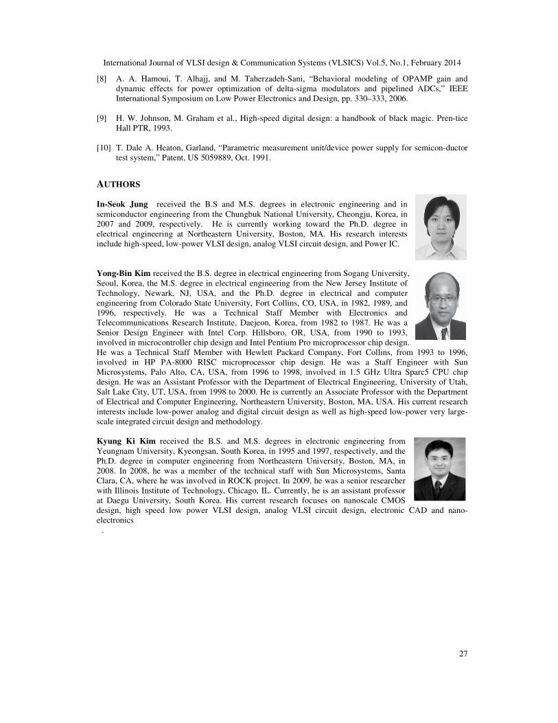
AUTHORS
In-Seok Jung received the B.S and M.S. degrees in electronic engineering and in
semiconductor engineering from the Chungbuk National University, Cheongju, Korea, in
2007 and 2009, respectively. He is currently working toward the Ph.D. degree in
electrical engineering at Northeastern University, Boston, MA. His research interests
include high-speed, low-power VLSI design, analog VLSI circuit design, and Power IC.
Yong-Bin Kim received the B.S. degree in electrical engineering from Sogang University,
Seoul, Korea, the M.S. degree in electrical engineering from the New Jersey Institute of
Technology, Newark, NJ, USA, and the Ph.D. degree in electrical and computer
engineering from Colorado State University, Fort Collins, CO, USA, in 1982, 1989, and
1996, respectively. He was a Technical Staff Member with Electronics and
Telecommunications Research Institute, Daejeon, Korea, from 1982 to 1987. He was a
Senior Design Engineer with Intel Corp. Hillsboro, OR, USA, from 1990 to 1993,
involved in microcontroller chip design and Intel Pentium Pro microprocessor chip design.
He was a Technical Staff Member with Hewlett Packard Company, Fort Collins, from 1993 to 1996,
involved in HP PA-8000 RISC microprocessor chip design. He was a Staff Engineer with Sun
Microsystems, Palo Alto, CA, USA, from 1996 to 1998, involved in 1.5 GHz Ultra Sparc5 CPU chip
design. He was an Assistant Professor with the Department of Electrical Engineering, University of Utah,
Salt Lake City, UT, USA, from 1998 to 2000. He is currently an Associate Professor with the Department
of Electrical and Computer Engineering, Northeastern University, Boston, MA, USA. His current research
interests include low-power analog and digital circuit design as well as high-speed low-power very large-
scale integrated circuit design and methodology.
Kyung Ki Kim received the B.S. and M.S. degrees in electronic engineering from
Yeungnam University, Kyeongsan, South Korea, in 1995 and 1997, respectively, and the
Ph.D. degree in computer engineering from Northeastern University, Boston, MA, in
2008. In 2008, he was a member of the technical staff with Sun Microsystems, Santa
Clara, CA, where he was involved in ROCK project. In 2009, he was a senior researcher
with Illinois Institute of Technology, Chicago, IL. Currently, he is an assistant professor
at Daegu University, South Korea. His current research focuses on nanoscale CMOS
design, high speed low power VLSI design, analog VLSI circuit design, electronic CAD and nano-
electronics
.