Copyright 2001, Agrawal & BushnellVLSI Test: Lecture 151 Memory market and memory complexity ...
65
Copyright 2001, Agrawal & Bushne ll VLSI Test: Lecture 15 1 Memory market and memory complexity Notation Faults and failures MATS+ March Test Memory fault models March test algorithms Inductive fault analysis Summary Lecture 15 Lecture 15 Memory Test Memory Test
-
date post
21-Dec-2015 -
Category
Documents
-
view
221 -
download
0
Transcript of Copyright 2001, Agrawal & BushnellVLSI Test: Lecture 151 Memory market and memory complexity ...

Copyright 2001, Agrawal & Bushnell
VLSI Test: Lecture 15 1
Memory market and memory complexity
Notation Faults and failures MATS+ March Test Memory fault models March test algorithms Inductive fault analysis Summary
Lecture 15Lecture 15Memory TestMemory Test
Lecture 15Lecture 15Memory TestMemory Test

Copyright 2001, Agrawal & Bushnell
VLSI Test: Lecture 15 2
Density and Defect Density and Defect TrendsTrends
Density and Defect Density and Defect TrendsTrends
1970 -- DRAM Invention (Intel) 1024 bits 1993 -- 1st 256 MBit DRAM papers 1997 -- 1st 256 MBit DRAM samples
1 /bit --> 120 X 10-6 /bit Kilburn -- Ferranti Atlas computer (Manchester
U.) -- Invented Virtual Memory 1997 -- Cache DRAM -- SRAM cache + DRAM
now on 1 chip
¢ ¢

Copyright 2001, Agrawal & Bushnell
VLSI Test: Lecture 15 3
Memory Cells Per ChipMemory Cells Per ChipMemory Cells Per ChipMemory Cells Per Chip

Copyright 2001, Agrawal & Bushnell
VLSI Test: Lecture 15 4
Test Time in SecondsTest Time in Seconds(Memory Size (Memory Size n Bitsn Bits))Test Time in SecondsTest Time in Seconds(Memory Size (Memory Size n Bitsn Bits))
n
1 Mb4 Mb
16 Mb64 Mb
256 Mb1 Gb2 Gb
n
0.060.251.014.03
16.1164.43128.9
n X log2n
1.265.5424.16104.7451.0
1932.83994.4
n3/2
64.5515.41.2 hr9.2 hr
73.3 hr586.4 hr
1658.6 hr
n2
18.3 hr293.2 hr
4691.3 hr75060.0 hr
1200959.9 hr19215358.4 hr76861433.7 hr
Size Number of Test Algorithm Operations

Copyright 2001, Agrawal & Bushnell
VLSI Test: Lecture 15 5
NotationNotationNotationNotation
0 -- A cell is in logical state 0 1 -- A cell is in logical state 1 X -- A cell is in logical state X A -- A memory address ABF -- AND Bridging Fault AF -- Address Decoder Fault B -- Memory # bits in a word BF -- Bridging Fault C -- A Memory Cell CF -- Coupling Fault
Copyright 2001, Agrawal & Bushnell
VLSI Test: Lecture 15 6
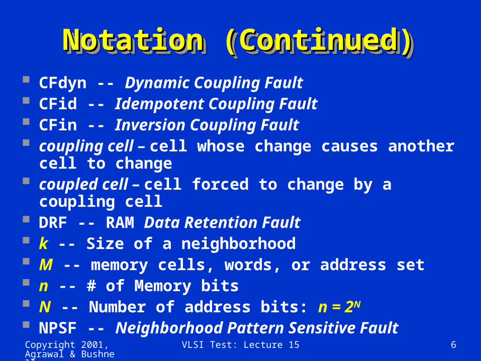
Notation (Continued)Notation (Continued)Notation (Continued)Notation (Continued) CFdyn -- Dynamic Coupling Fault CFid -- Idempotent Coupling Fault CFin -- Inversion Coupling Fault coupling cell – cell whose change causes
another cell to change coupled cell – cell forced to change by a
coupling cell DRF -- RAM Data Retention Fault k -- Size of a neighborhood M -- memory cells, words, or address set n -- # of Memory bits N -- Number of address bits: n = 2N
NPSF -- Neighborhood Pattern Sensitive Fault

Copyright 2001, Agrawal & Bushnell
VLSI Test: Lecture 15 7
Notation (Continued)Notation (Continued)Notation (Continued)Notation (Continued)
OBF -- OR Bridging Fault SAF -- Stuck-at Fault SCF -- State Coupling Fault SOAF -- Stuck-Open Address
Decoder Fault TF -- Transition Fault

Copyright 2001, Agrawal & Bushnell
VLSI Test: Lecture 15 8
FaultsFaultsFaultsFaults
System -- Mixed electronic, electromechanical, chemical, and photonic system (MEMS technology)
Failure -- Incorrect or interrupted system behavior
Error -- Manifestation of fault in system Fault -- Physical difference between
good & bad system behavior
Copyright 2001, Agrawal & Bushnell
VLSI Test: Lecture 15 9
Fault TypesFault TypesFault TypesFault Types
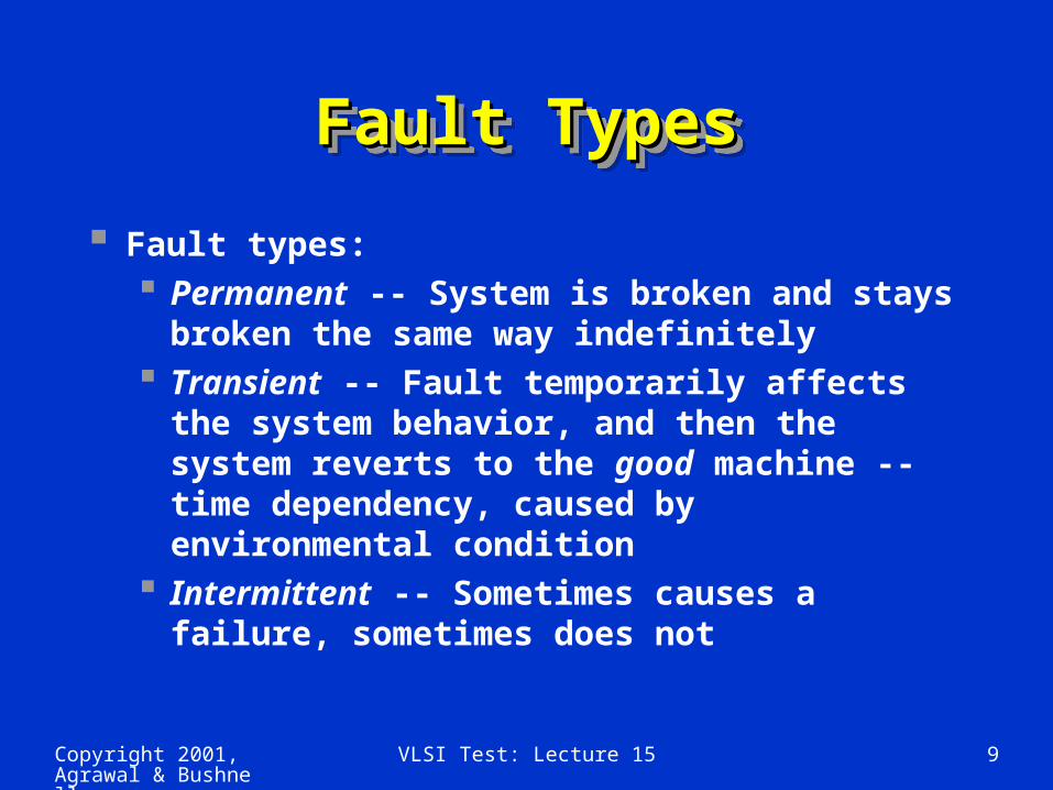
Fault types: Permanent -- System is broken and
stays broken the same way indefinitely Transient -- Fault temporarily affects
the system behavior, and then the system reverts to the good machine -- time dependency, caused by environmental condition
Intermittent -- Sometimes causes a failure, sometimes does not

Copyright 2001, Agrawal & Bushnell
VLSI Test: Lecture 15 10
Failure MechanismsFailure MechanismsFailure MechanismsFailure Mechanisms
Permanent faults: Missing/Added Electrical Connection Broken Component (IC mask defect or
silicon-to-metal connection) Burnt-out Chip Wire Corroded connection between chip &
package Chip logic error (Pentium division bug)

Copyright 2001, Agrawal & Bushnell
VLSI Test: Lecture 15 11
Failure Mechanisms Failure Mechanisms (Continued)(Continued)
Failure Mechanisms Failure Mechanisms (Continued)(Continued)
Transient Faults: Cosmic Ray An particle (ionized Helium atom) Air pollution (causes wire short/open) Humidity (temporary short) Temperature (temporary logic error) Pressure (temporary wire open/short) Vibration (temporary wire open) Power Supply Fluctuation (logic error) Electromagnetic Interference (coupling) Static Electrical Discharge (change state) Ground Loop (misinterpreted logic value)

Copyright 2001, Agrawal & Bushnell
VLSI Test: Lecture 15 12
Failure Mechanisms Failure Mechanisms (Continued)(Continued)
Failure Mechanisms Failure Mechanisms (Continued)(Continued)
Intermittent Faults: Loose Connections Aging Components (changed logic delays) Hazards and Races in critical timing paths
(bad design) Resistor, Capacitor, Inductor variances
(timing faults) Physical Irregularities (narrow wire -- high
resistance) Electrical Noise (memory state changes)

Copyright 2001, Agrawal & Bushnell
VLSI Test: Lecture 15 13
Physical Failure Physical Failure MechanismsMechanisms
Physical Failure Physical Failure MechanismsMechanisms
Corrosion Electromigration Bonding Deterioration -- Au package wires
interdiffuse with Al chip pads Ionic Contamination -- Na+ diffuses through
package and into FET gate oxide Alloying -- Al migrates from metal layers into
Si substrate Radiation and Cosmic Rays -- 8 MeV, collides
with Si lattice, generates n - p pairs, causes soft memory error
Copyright 2001, Agrawal & Bushnell
VLSI Test: Lecture 15 14
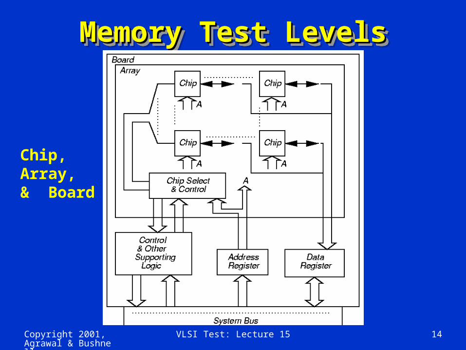
Memory Test LevelsMemory Test LevelsMemory Test LevelsMemory Test Levels
Chip, Array, & Board

Copyright 2001, Agrawal & Bushnell
VLSI Test: Lecture 15 15
March Test NotationMarch Test NotationMarch Test NotationMarch Test Notation r -- Read a memory location
w -- Write a memory location
r0 -- Read a 0 from a memory location
r1 -- Read a 1 from a memory location
w0 -- Write a 0 to a memory location
w1 -- Write a 1 to a memory location
-- Write a 1 to a cell containing 0
-- Write a 0 to a cell containing 1

Copyright 2001, Agrawal & Bushnell
VLSI Test: Lecture 15 16
March Test Notation March Test Notation (Continued)(Continued)
March Test Notation March Test Notation (Continued)(Continued)
-- Complement the cell contents
-- Increasing memory addressing
-- Decreasing memory addressing
-- Either increasing or decreasing

Copyright 2001, Agrawal & Bushnell
VLSI Test: Lecture 15 17
More March Test More March Test NotationNotation
More March Test More March Test NotationNotation
-- Any write operation < ... > -- Denotes a particular fault, ... <I / F > -- I is the fault sensitizing condition,
F is the faulty cell value <I1, ..., In-1 ; In / F> -- Denotes a fault
covering n cells I1, ..., In-1 are fault sensitization
conditions in cells 1 through n - 1 for cell n In gives sensitization condition for cell n If In is empty, write In / F as F
A

Copyright 2001, Agrawal & Bushnell
VLSI Test: Lecture 15 18
MATS+ March TestMATS+ March TestMATS+ March TestMATS+ March TestM0: { March element (w0) }
for cell := 0 to n - 1 (or any other order) dowrite 0 to A [cell];
M1: { March element (r0, w1) }for cell := 0 to n - 1 do
read A [cell]; { Expected value = 0}write 1 to A [cell];
M2: {March element (r1, w0) }for cell := n – 1 down to 0 do
read A [cell]; { Expected value = 1 }write 0 to A [cell];

Copyright 2001, Agrawal & Bushnell
VLSI Test: Lecture 15 19
Fault ModelingFault ModelingFault ModelingFault Modeling
Behavioral (black-box) Model -- State machine modeling all memory content combinations -- Intractable
Functional (gray-box) Model -- Used
Logic Gate Model -- Not used Inadequately models transistors & capacitors
Electrical Model -- Very expensive
Geometrical Model -- Layout Model
Used with Inductive Fault Analysis

Copyright 2001, Agrawal & Bushnell
VLSI Test: Lecture 15 20
Functional ModelFunctional ModelFunctional ModelFunctional Model

Copyright 2001, Agrawal & Bushnell
VLSI Test: Lecture 15 21
Simplified Functional Simplified Functional ModelModel
Simplified Functional Simplified Functional ModelModel

Copyright 2001, Agrawal & Bushnell
VLSI Test: Lecture 15 22
Reduced Functional Reduced Functional Model (van de Goor)Model (van de Goor)Reduced Functional Reduced Functional Model (van de Goor)Model (van de Goor)
n Memory bits, B bits/word, n/B addresses
Access happens when Address Latch contents change
Low-order address bits operate column decoder, high-order operate row decoder
read -- Precharge bit lines, then activate row
write -- Keep driving bit lines during evaluation
Refresh -- Read all bits in 1 row and simultaneously refresh them

Copyright 2001, Agrawal & Bushnell
VLSI Test: Lecture 15 23
Subset Functional Subset Functional FaultsFaults
Subset Functional Subset Functional FaultsFaults
abcdefgh
Functional faultCell stuckDriver stuckRead/write line stuckChip-select line stuckData line stuckOpen circuit in data lineShort circuit between data linesCrosstalk between data lines
Copyright 2001, Agrawal & Bushnell
VLSI Test: Lecture 15 24
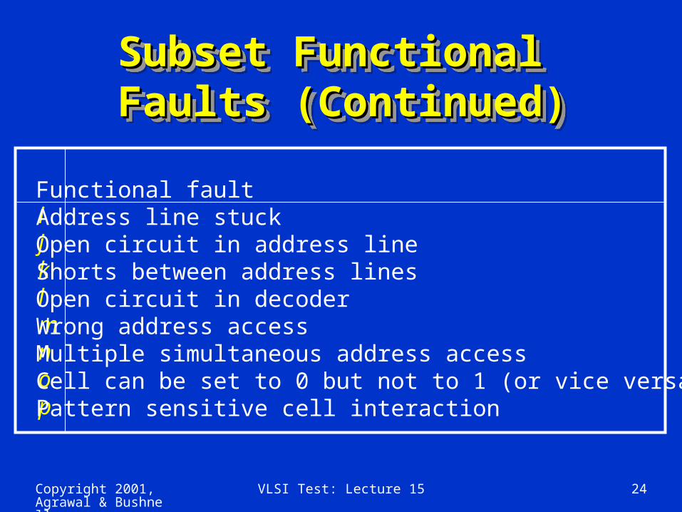
Subset Functional Subset Functional Faults (Continued)Faults (Continued)Subset Functional Subset Functional Faults (Continued)Faults (Continued)
ijklmnop
Functional faultAddress line stuckOpen circuit in address lineShorts between address linesOpen circuit in decoderWrong address accessMultiple simultaneous address accessCell can be set to 0 but not to 1 (or vice versa)Pattern sensitive cell interaction

Copyright 2001, Agrawal & Bushnell
VLSI Test: Lecture 15 25
Reduced Functional Reduced Functional FaultsFaults
Reduced Functional Reduced Functional FaultsFaults
SAFTFCFNPSF
FaultStuck-at faultTransition faultCoupling faultNeighborhood Pattern Sensitive fault
Copyright 2001, Agrawal & Bushnell
VLSI Test: Lecture 15 26
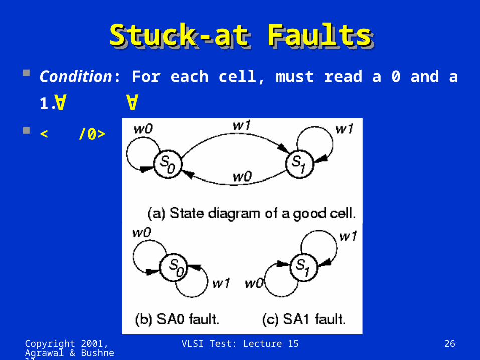
Stuck-at FaultsStuck-at FaultsStuck-at FaultsStuck-at Faults Condition: For each cell, must read a 0 and a
1.
< /0> (< /1>)
A A

Copyright 2001, Agrawal & Bushnell
VLSI Test: Lecture 15 27
Transition FaultsTransition FaultsTransition FaultsTransition Faults Cell fails to make 0 1 or 1 0 transition
Condition: Each cell must undergo a
transition and a transition, and be read
after such, before undergoing any further
transitions.
< /0>, < /1>
< /0> transition fault

Copyright 2001, Agrawal & Bushnell
VLSI Test: Lecture 15 28
Coupling FaultsCoupling FaultsCoupling FaultsCoupling Faults
Coupling Fault (CF): Transition in bit j causes unwanted change in bit i
2-Coupling Fault: Involves 2 cells, special case of k-Coupling Fault Must restrict k cells to make practical
Inversion and Idempotent CFs -- special cases of 2-Coupling Faults
Bridging and State Coupling Faults involve any # of cells, caused by logic level
Dynamic Coupling Fault (CFdyn) -- Read or write on j forces i to 0 or 1

Copyright 2001, Agrawal & Bushnell
VLSI Test: Lecture 15 29
Inversion Coupling Inversion Coupling Faults (CFin)Faults (CFin)
Inversion Coupling Inversion Coupling Faults (CFin)Faults (CFin)
or in cell j inverts contents of cell i
Condition: For all cells that are coupled,
each should be read after a series of
possible CFins may have occurred, and
the # of coupled cell transitions must be
odd (to prevent the CFins from masking
each other).
< ; > and < ; >

Copyright 2001, Agrawal & Bushnell
VLSI Test: Lecture 15 30
Good Machine State Good Machine State Transition DiagramTransition Diagram
Good Machine State Good Machine State Transition DiagramTransition Diagram

Copyright 2001, Agrawal & Bushnell
VLSI Test: Lecture 15 31
CFin State Transition CFin State Transition DiagramDiagram
CFin State Transition CFin State Transition DiagramDiagram
Copyright 2001, Agrawal & Bushnell
VLSI Test: Lecture 15 32
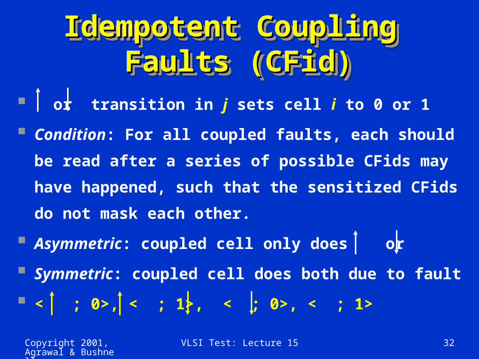
Idempotent Coupling Idempotent Coupling Faults (CFid)Faults (CFid)
Idempotent Coupling Idempotent Coupling Faults (CFid)Faults (CFid)
or transition in j sets cell i to 0 or 1
Condition: For all coupled faults, each should
be read after a series of possible CFids may
have happened, such that the sensitized CFids
do not mask each other.
Asymmetric: coupled cell only does or
Symmetric: coupled cell does both due to fault
< ; 0>, < ; 1>, < ; 0>, < ; 1>

Copyright 2001, Agrawal & Bushnell
VLSI Test: Lecture 15 33
CFid ExampleCFid ExampleCFid ExampleCFid Example

Copyright 2001, Agrawal & Bushnell
VLSI Test: Lecture 15 34
Dynamic Coupling Dynamic Coupling Faults (CFdyn)Faults (CFdyn)
Dynamic Coupling Dynamic Coupling Faults (CFdyn)Faults (CFdyn)
Read or write in cell of 1 word forces cell in different word to 0 or 1
<r0 | w0 ; 0>, <r0 | w0 ; 1>, < r1 | w1 ; 0>, and <r1 | w1; 1>
| Denotes “OR” of two operations
More general than CFid, because a CFdyn can be sensitized by any read or write operation

Copyright 2001, Agrawal & Bushnell
VLSI Test: Lecture 15 35
Bridging FaultsBridging FaultsBridging FaultsBridging Faults
Short circuit between 2+ cells or lines
0 or 1 state of coupling cell, rather than coupling cell transition, causes coupled cell change
Bidirectional fault -- i affects j, j affects i
AND Bridging Faults (ABF): < 0,0 / 0,0 >, <0,1 / 0,0 >, <1,0 / 0,0>, <1,1 / 1,1>
OR Bridging Faults (OBF): < 0,0 / 0,0 >, <0,1 / 1,1 >, <1,0 / 1,1>, <1,1 / 1,1>

Copyright 2001, Agrawal & Bushnell
VLSI Test: Lecture 15 36
State Coupling FaultsState Coupling FaultsState Coupling FaultsState Coupling Faults Coupling cell / line j is in a given state y that
forces coupled cell / line i into state x < 0;0 >, < 0;1 >, < 1;0 >, < 1;1 >
Copyright 2001, Agrawal & Bushnell
VLSI Test: Lecture 15 37
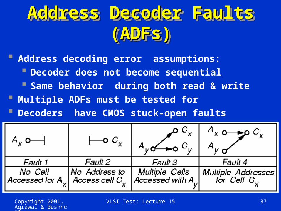
Address Decoder Faults Address Decoder Faults (ADFs)(ADFs)
Address Decoder Faults Address Decoder Faults (ADFs)(ADFs)
Address decoding error assumptions: Decoder does not become sequential Same behavior during both read & write
Multiple ADFs must be tested for Decoders have CMOS stuck-open faults

Copyright 2001, Agrawal & Bushnell
VLSI Test: Lecture 15 38
Theorem 9.2Theorem 9.2Theorem 9.2Theorem 9.2 A March test satisfying conditions 1 & 2 detects
all address decoder faults. ... Means any # of read or write operations Before condition 1, must have wx element
x can be 0 or 1, but must be consistent in test
Condition
1
2
March element
(rx, …, w x )
(r x , …, wx)

Copyright 2001, Agrawal & Bushnell
VLSI Test: Lecture 15 39
Proof IllustrationProof IllustrationProof IllustrationProof Illustration

Copyright 2001, Agrawal & Bushnell
VLSI Test: Lecture 15 40
Necessity ProofNecessity ProofNecessity ProofNecessity Proof
Removing rx from Condition 1 prevents A or B fault detection when x read
Removing rx from Condition 2 prevents A or B fault detection when x read
Removing rx or wx from Condition 1 misses fault D2
Removing rx or wx from condition 2 misses fault D3
Removing both writes misses faults C and D1
Copyright 2001, Agrawal & Bushnell
VLSI Test: Lecture 15 41
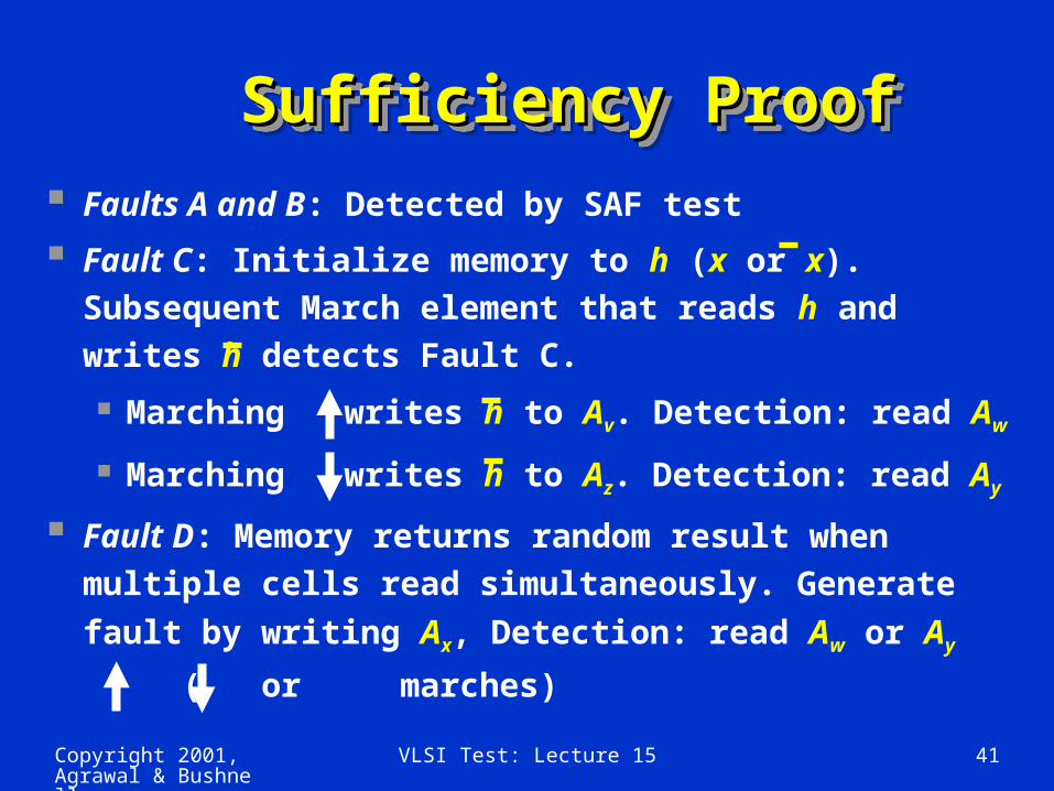
Sufficiency ProofSufficiency Proof Sufficiency ProofSufficiency Proof Faults A and B: Detected by SAF test
Fault C: Initialize memory to h (x or x). Subsequent March element that reads h and writes h detects Fault C.
Marching writes h to Av. Detection: read Aw
Marching writes h to Az. Detection: read Ay
Fault D: Memory returns random result when multiple cells read simultaneously. Generate
fault by writing Ax, Detection: read Aw or Ay
( or marches)

Copyright 2001, Agrawal & Bushnell
VLSI Test: Lecture 15 42
Reduced Functional FaultsReduced Functional FaultsReduced Functional FaultsReduced Functional FaultsFaultSAFSAFSAFSAFSAFSAFCFCFAFAFAFAFAFAFTFNPSF
abcdefghijkl
mnop
Functional faultCell stuckDriver stuckRead/write line stuckChip-select line stuckData line stuckOpen circuit in data lineShort circuit between data linesCrosstalk between data linesAddress line stuckOpen circuit in address lineShorts between address linesOpen circuit in decoderWrong address accessMultiple simultaneous address accessCell can be set to 0 (1) but not to 1 (0)Pattern sensitive cell interaction
Copyright 2001, Agrawal & Bushnell
VLSI Test: Lecture 15 43
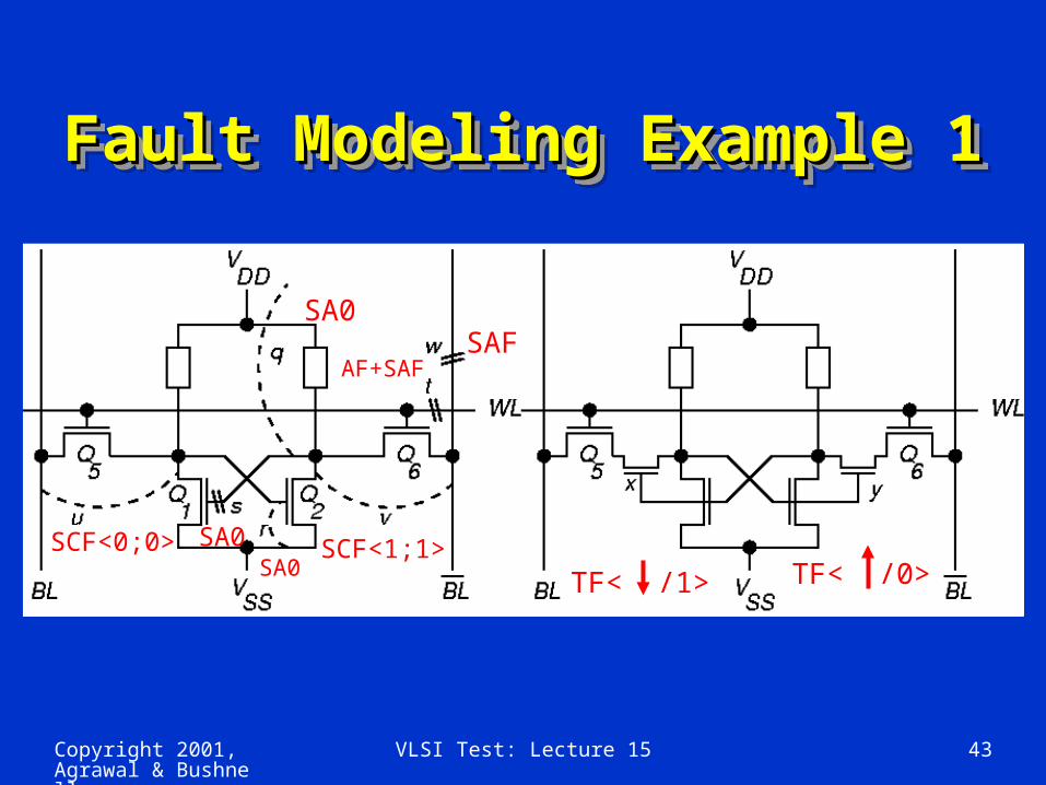
Fault Modeling Example 1Fault Modeling Example 1Fault Modeling Example 1Fault Modeling Example 1
SCF<0;0>
SA0
SCF<1;1>
AF+SAFSAF
SA0SA0
TF< /1> TF< /0>

Copyright 2001, Agrawal & Bushnell
VLSI Test: Lecture 15 44
Fault Modeling Example 2Fault Modeling Example 2Fault Modeling Example 2Fault Modeling Example 2
ABF
ABF
SA0
ABF
SA1 SA1+SCF
SCF
gg

Copyright 2001, Agrawal & Bushnell
VLSI Test: Lecture 15 45
Multiple Fault ModelsMultiple Fault ModelsMultiple Fault ModelsMultiple Fault Models Coupling Faults: In real manufacturing, any #
can occur simultaneously
Linkage: A fault influences behavior of another
Example March test that fails:
{ (w0) ; (r0, w1); (w0, w1); (r1)}
Works only when faults not linked

Copyright 2001, Agrawal & Bushnell
VLSI Test: Lecture 15 46
Fault HierarchyFault HierarchyFault HierarchyFault Hierarchy

Copyright 2001, Agrawal & Bushnell
VLSI Test: Lecture 15 47
Tests for Linked AFsTests for Linked AFsTests for Linked AFsTests for Linked AFs Cases 1, 2, 3 & 5 -- Unlinked Cases 4 & 6 -- Linked

Copyright 2001, Agrawal & Bushnell
VLSI Test: Lecture 15 48
DRAM/SRAM Fault ModelingDRAM/SRAM Fault ModelingDRAM/SRAM Fault ModelingDRAM/SRAM Fault Modeling
DRAM or SRAM FaultsShorts & opens in memory cell arrayShorts & opens in address decoderAccess time failures in address decoderCoupling capacitances between cellsBit line shorted to word lineTransistor gate shorted to channelTransistor stuck-open faultPattern sensitive fault Diode-connected transistor 2 cell short Open transistor drain Gate oxide short Bridging fault
ModelSAF,SCF
AFFunctional
CFIDDQIDDQSOFPSF

Copyright 2001, Agrawal & Bushnell
VLSI Test: Lecture 15 49
SRAM Only Fault ModelingSRAM Only Fault ModelingSRAM Only Fault ModelingSRAM Only Fault Modeling
Faults found only in SRAMOpen-circuited pull-up deviceExcessive bit line coupling capacitance
ModelDRFCF
Copyright 2001, Agrawal & Bushnell
VLSI Test: Lecture 15 50
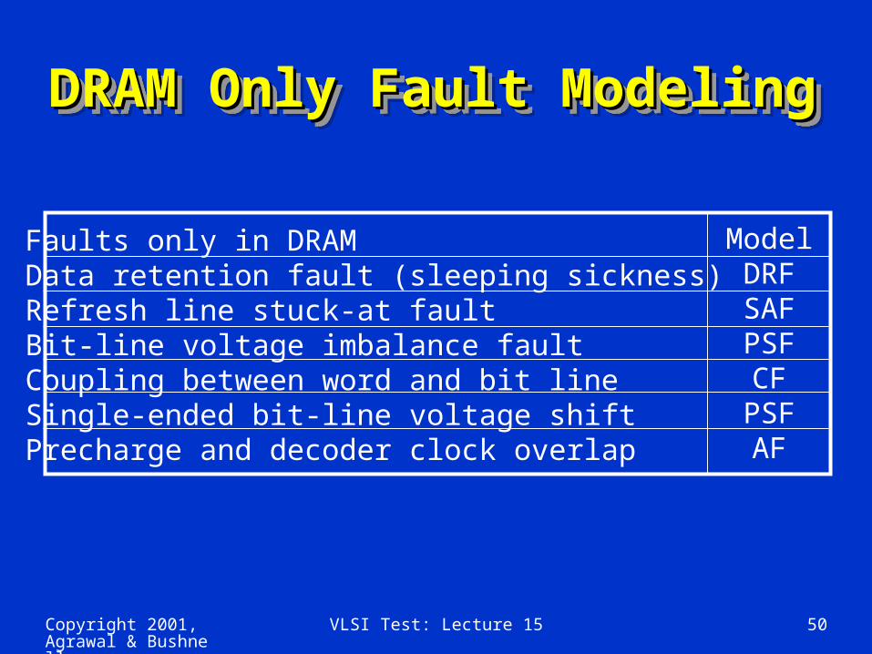
DRAM Only Fault DRAM Only Fault ModelingModeling
DRAM Only Fault DRAM Only Fault ModelingModeling
Faults only in DRAMData retention fault (sleeping sickness)Refresh line stuck-at faultBit-line voltage imbalance faultCoupling between word and bit lineSingle-ended bit-line voltage shiftPrecharge and decoder clock overlap
ModelDRFSAFPSFCFPSFAF

Copyright 2001, Agrawal & Bushnell
VLSI Test: Lecture 15 51
Test Influence on SRAM Test Influence on SRAM Fault Coverage Fault Coverage
Test Influence on SRAM Test Influence on SRAM Fault Coverage Fault Coverage

Copyright 2001, Agrawal & Bushnell
VLSI Test: Lecture 15 52
Influence of Addressing Influence of Addressing Order on Fault CoverageOrder on Fault CoverageInfluence of Addressing Influence of Addressing Order on Fault CoverageOrder on Fault Coverage

Copyright 2001, Agrawal & Bushnell
VLSI Test: Lecture 15 53
Critical Path LengthCritical Path LengthCritical Path LengthCritical Path Length Length of parallel wires separated by
dimension of spot defect size TFs and CFids happen only on long wires
Fault class
Stuck-atStuck-openTransitionState Coup.Idemp. Coup.Data retentionTotal
<278320
150
27152
<32136436150
29357
<52276438510
80460
<72696438710
80522
<92696438711880
540
<251.3%21.0%
0%9.9%0%
17.8%100%
<949.8%11.9%7.0%
13.2%3.3%
14.8%100%
Spot defect size (m)

Copyright 2001, Agrawal & Bushnell
VLSI Test: Lecture 15 54
Fault FrequencyFault FrequencyFault FrequencyFault Frequency Obtained with Scanning Electron Microscope CFin and TF faults rarely occurred
Cluster0123457--14
# Devices7141691898526--2
Fault classStuck-at and Total failureStuck-openIdempotent couplingState coupling??Data retention??

Copyright 2001, Agrawal & Bushnell
VLSI Test: Lecture 15 55
Functional RAM Testing Functional RAM Testing with March Testswith March Tests
Functional RAM Testing Functional RAM Testing with March Testswith March Tests
March Tests can detect AFs -- NPSF Tests Cannot
Conditions for AF detection:
Need ( r x, w x)
Need ( r x, w x)
In the following March tests, addressing orders can be interchanged

Copyright 2001, Agrawal & Bushnell
VLSI Test: Lecture 15 56
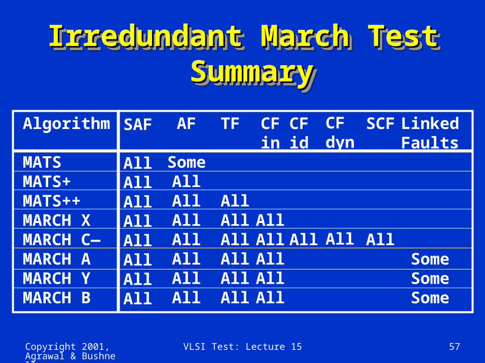
Irredundant March TestsIrredundant March TestsIrredundant March TestsIrredundant March TestsAlgorithm
MATSMATS+
MATS++MARCH XMARCH
C—MARCH A
MARCH YMARCH B
Description{ (w0); (r0, w1); (r1) }
{ (w0); (r0, w1); (r1, w0) }{ (w0); (r0, w1); (r1, w0, r0) }
{ (w0); (r0, w1); (r1, w0); (r0) }{ (w0); (r0, w1); (r1, w0); (r0, w1); (r1, w0); (r0) }
{ (w0); (r0, w1, w0, w1); (r1, w0, w1); (r1, w0, w1, w0); (r0, w1, w0) }
{ (w0); (r0, w1, r1); (r1, w0, r0); (r0) }{ (w0); (r0, w1, r1, w0, r0, w1);
(r1, w0, w1); (r1, w0, w1, w0);(r0, w1, w0) }
Copyright 2001, Agrawal & Bushnell
VLSI Test: Lecture 15 57
Irredundant March Test Irredundant March Test Summary Summary
Irredundant March Test Irredundant March Test Summary Summary
Algorithm
MATSMATS+MATS++MARCH XMARCH C—MARCH AMARCH YMARCH B
SAF
AllAllAllAllAllAllAllAll
AF
SomeAllAllAllAllAllAllAll
TF
AllAllAllAllAllAll
CFin
AllAllAllAllAll
CFid
All
CFdyn
All
SCF
All
LinkedFaults
SomeSomeSome

Copyright 2001, Agrawal & Bushnell
VLSI Test: Lecture 15 58
March Test ComplexityMarch Test ComplexityMarch Test ComplexityMarch Test Complexity
AlgorithmMATS
MATS+MATS++MARCH X
MARCH C—MARCH AMARCH YMARCH B
Complexity4n5n6n6n10n15n8n17n

Copyright 2001, Agrawal & Bushnell
VLSI Test: Lecture 15 59
MATS+ ExampleMATS+ ExampleCell (2,1) SA0 FaultCell (2,1) SA0 Fault
MATS+ ExampleMATS+ ExampleCell (2,1) SA0 FaultCell (2,1) SA0 Fault
MATS+:{ M0: (w0); M1: (r0, w1); M2: (r1, w0) }

Copyright 2001, Agrawal & Bushnell
VLSI Test: Lecture 15 60
MATS+ ExampleMATS+ ExampleCell (2, 1) SA1 FaultCell (2, 1) SA1 Fault
MATS+ ExampleMATS+ ExampleCell (2, 1) SA1 FaultCell (2, 1) SA1 Fault
MATS+:{ M0: (w0); M1: (r0, w1); M2: (r1, w0) }

Copyright 2001, Agrawal & Bushnell
VLSI Test: Lecture 15 61
MATS+ ExampleMATS+ ExampleMultiple AF Type CMultiple AF Type CMATS+ ExampleMATS+ Example
Multiple AF Type CMultiple AF Type C Cell (2,1) is not addressable Address (2,1) maps into (3,1) & vice versa Can’t write (2,1), read (2,1) gives random #
MATS+:{ M0: (w0); M1: (r0, w1); M2: (r1), w0 }

Copyright 2001, Agrawal & Bushnell
VLSI Test: Lecture 15 62
RAM Tests for Layout-RAM Tests for Layout-Related FaultsRelated Faults
RAM Tests for Layout-RAM Tests for Layout-Related FaultsRelated Faults
Inductive Fault Analysis:1 Generate defect sizes, location, layers
based on fabrication line model2 Place defects on layout model3 Extract defective cell schematic &
electrical parameters4 Evaluate cell testing, using VLASIC Dekker found these faults:
SAF, SOF, TF, SCF, CFid, DRF Proposed IFA-9 March test Delay means wait 100 ms

Copyright 2001, Agrawal & Bushnell
VLSI Test: Lecture 15 63
Inductive Fault Analysis Inductive Fault Analysis March Tests March Tests
Inductive Fault Analysis Inductive Fault Analysis March Tests March Tests
Algor-ithmIFA-9
IFA-13
SAFAllAll
TFAllAll
AFAllAll
SOF
All
SCFAllAll
CFidAllAll
DRFAllAll
Operations12n+Delays16n+Delays
Physical Defect Fault Coverage
Algor-ithmIFA-9
IFA-13
Description{ (w0); (r0, w1); (r1, w0); (r0, w1);
(r1, w0); Delay; (r0, w1); Delay; (r1) }{ (w0); (r0, w1, r1); (r1, w0, r0);
(r0, w1, r1), (r1, w0, r0),Delay; (r0, w1); Delay; (r1) }

Copyright 2001, Agrawal & Bushnell
VLSI Test: Lecture 15 64
IFA Test ValidationIFA Test ValidationIFA Test ValidationIFA Test Validation Higher scores show better tests
TestMATS+
MATS+ and DelayMarch C
March C and DelayIFA-9 and Delay
IFA-13IFA-13 and Delay
Score7186189918092
Test Time5n
8n + 2 Delay11n
14n + 2 Delay12n + 2 Delay
13n16n + 2 Delay

Copyright 2001, Agrawal & Bushnell
VLSI Test: Lecture 15 65
Memory Testing Memory Testing SummarySummary
Memory Testing Memory Testing SummarySummary
Multiple fault models are essential Combination of tests is essential:
March – SRAM and DRAM NPSF -- DRAM DC Parametric -- Both AC Parametric -- Both
Inductive Fault Analysis is now required