Copper-Nanoparticles as a Catalyst for InAs-Nanowire ...
15
Copper-Nanoparticles as a Catalyst for InAs-Nanowire Growth during Molecular Beam Epitaxy Laust Raahauge nht 444 June 9, 2015 Supervisors: Jessica Bolinsson Jesper Nyg˚ ard 1
Transcript of Copper-Nanoparticles as a Catalyst for InAs-Nanowire ...

Copper-Nanoparticles as a Catalyst for InAs-Nanowire
Growth during Molecular Beam Epitaxy
Laust Raahauge
nht 444
June 9, 2015
Supervisors:
Jessica Bolinsson
Jesper Nygard
1

1 Abstract
We study the usefulness of copper as a catalyst for the growth of InAs nanowires in a
MBE-system. The project focuses on characterization of surface crystals using scanning
electron microscopy. After first confirming that annealing causes a thin Cu-layer to
form nanoparticles, growth is attempted at different temperatures on (111)B and (001)
oriented surfaces. Finally, there is found no convincing proof of free-standing NWs,
however onedimensional crystals are found growing horizonthally along the surface, with
roughly the same dimensions as short nanowires.
2 introduction
Limitting the size of a semiconducting crystal in two dimensions to form a nanowire can
have uses in different fields within modern physics[1][2].Physically, 1d and 2d structures
confines conducting electrons so a more discrete set of energies are allowed. They are
also characterized by a large surface compared to conductivity, which is practical for
nano sensors.
Luckily, methods have been discovered, and are being refined, for creating nanowires
with diameters less than 50 nm by epitaxial growth, where one can achieve both very
high purity of the material as well as some control over the crystal structure of the
wires[3].
The most common way to start such a growth is to deposit droplets, also called seed-
particles, of a catalyst metal, usually gold, on a clean substrate, anneal the particles by
heating them in a vacuum and then add the desired material either through chemical
processes involving vapour as a carrying medium(for instance in metal-organic vapour
epitaxy (MOVPE)) or as a beam of atoms(Molecular Beam Epitaxy, which was used
in this project). Sometimes the anneal needs to take place within a flux of some of
the materials of the substrate, to prevent dissipation, in particular arsenic is prone to
dissipate at annealing temperatures.
The end result is wires standing as columns with heights, or lengths, up to many mi-
crometers and diameters down to 10 nanometers. Oftentime the seedparticle remain at
the top while the wire grows beneath it. A perceived similarity to standing hairs earned
the wires the name nanowhiskers in some older litterature.
The growth process is not yet completely understood, however the Vapour-Liquid-
Solid(VLS) model gives an explanation[4], where the gold particles are assumed to be
liquid droplets at the growth temperature. Incoming particles from the vapour or beam
1

will often diffuse along the substrate until they reach a droplet, where they might be ab-
sorbed. As a result the droplets becomes supersaturated with material, and the surplus
can then pass to the solid phase, merging with the substrate below the droplet.
Apart from gold other metals such as silver and copper have been found to act as a
catalyst for the VLS-proces[5][6]. Also, though not quite understood yet, catalyst-free
”selfseeded” nanowires have been grown in recent years[7].
This project also serve as an introduction for me to some experimental methods, most
importantly electron microscopy. The use of the plural first person throughout the text
reflects the cooperation with my supervisor Jessica Bolinsson and others on the Qdev at
NBI. My own contribution mainly consist in the examination and evaluation, while the
actual growth were handled by more experienced staff. All pictures used were taken by
me.
2.1 Seedparticles and Annealing
As mentioned most epitaxial growth of NW relies on nanoparticles of a certain metal,
with diameters less than 100nm. They can either be deposited directly on the surface as
aerosol, or created in-situ by heating a thin metal layer until it breaks up into islands.
The latter method has the added bonus that the heating also anneals the seedparti-
cles, removing impurities and oxygen by degassing and deoxidizing. Studies[8][9] have
also shown that the annealing causes the catalyst metal to interact with the substrate,
forming an ultrathin wetting layer with particles integrating into the substrate crys-
tal structure. Another result of the annealing is reconfigurations of the surface, which
can cause cracks and reefs that can interfere with particle diffusion and so inhibit NW
growth. Usually the conditions can be adjusted to minimize the latter effect, but seeing
as we are in unchartered territory with the copper, the reconfiguration played a major
role in this project.
2.2 Substrates
NWs are usually grown both from and on very pure crystals of semiconducting elements.
Silicon are often used, and so are III-V-group compounds, like GaAs or InAs. This is
obviously part of the attractiveness of the field as the same substances are already used
in sophisticated electronics.
The crystal structure of the substrate can also be determining for the directions in which
NW’s wil grow. When using a cubic zincblende substrate the wires are often found to
grow in the (111) direction[10]. The surface is therefore usually given a (111) orientation
2
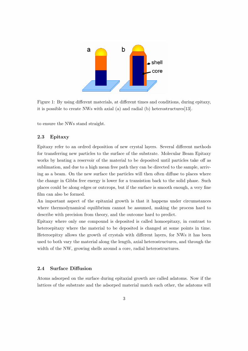
Figure 1: By using different materials, at different times and conditions, during epitaxy,
it is possible to create NWs with axial (a) and radial (b) heterostructures[13].
to ensure the NWs stand straight.
2.3 Epitaxy
Epitaxy refer to an ordred deposition of new crystal layers. Several different methods
for transferring new particles to the surface of the substrate. Molecular Beam Epitaxy
works by heating a reservoir of the material to be deposited until particles take off as
sublimation, and due to a high mean free path they can be directed to the sample, arriv-
ing as a beam. On the new surface the particles will then often diffuse to places where
the change in Gibbs free energy is lower for a transistion back to the solid phase. Such
places could be along edges or outcrops, but if the surface is smooth enough, a very fine
film can also be formed.
An important aspect of the epitaxial growth is that it happens under circumstances
where thermodynamical equilibrium cannot be assumed, making the process hard to
describe with precision from theory, and the outcome hard to predict.
Epitaxy where only one compound is deposited is called homoepitaxy, in contrast to
heteroepitaxy where the material to be deposited is changed at some points in time.
Heteroepitxy allows the growth of crystals with different layers, for NWs it has been
used to both vary the material along the length, axial heterostructures, and through the
width of the NW, growing shells around a core, radial heterostructures.
2.4 Surface Diffusion
Atoms adsorped on the surface during epitaxial growth are called adatoms. Now if the
lattices of the substrate and the adsorped material match each other, the adatoms will
3
(a)
(b)
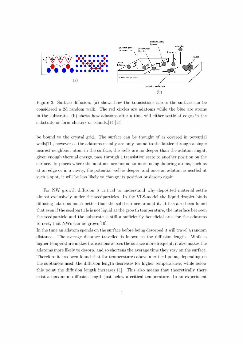
Figure 2: Surface diffusion, (a) shows how the transistions across the surface can be
considered a 2d random walk. The red circles are adatoms while the blue are atoms
in the substrate. (b) shows how adatoms after a time will either settle at edges in the
substrate or form clusters or islands.[14][15]
be bound to the crystal grid. The surface can be thought of as covered in potential
wells[11], however as the adatoms usually are only bound to the lattice through a single
nearest neighbour-atom in the surface, the wells are no deeper than the adatom might,
given enough thermal energy, pass through a transistion state to another position on the
surface. In places where the adatoms are bound to more neiughbouring atoms, such as
at an edge or in a cavity, the potential well is deeper, and once an adatom is nestled at
such a spot, it will be less likely to change its position or desorp again.
For NW growth diffusion is critical to understand why deposited material settle
almost exclusively under the seedparticles. In the VLS-model the liquid droplet binds
diffusing adatoms much better than the solid surface around it. It has also been found
that even if the seedparticle is not liquid at the growth temperature, the interface between
the seedparticle and the substrate is still a sufficiently beneficial area for the adatoms
to nest, that NWs can be grown[10].
In the time an adatom spends on the surface before being desorped it will travel a random
distance. The average distance travelled is known as the diffusion length. While a
higher temperature makes transistions across the surface more frequent, it also makes the
adatoms more likely to desorp, and so shortens the average time they stay on the surface.
Therefore it has been found that for temperatures above a critical point, depending on
the subtances used, the diffusion length decreases for higher temperatures, while below
this point the diffusion length increases[11]. This also means that theoretically there
exist a maximum diffusion length just below a critical temperature. In an experiment
4

by Linus E. Jensen et al. InAs NWs were grown in a hexagonal pattern[17]. It was found
that when the seperation between the NWs were less than the diffusion length (found
to be a few µm) the NWs competed for material. The effect was that the growth rate
of the NWs were proportional to the logarithm of the seperation distance.
2.5 Electron Microscopy
To observe structures with dimensions of less than 100 nm, visible light would be useless
due to its relatively high wavelength and diffraction limit. We therefore rely on electron
microscopy, either scanning (SEM) where a beam being probed over a region causes
the surface to emit secondary electrons which can be detected to determine the obseved
topography, or transmission (TEM) where electrons pass through the sample before
reaching a detector. While TEM can achieve much higher resolution than SEM, it relies
on the sample to be ultra thin and in a well defined position. For these reasons this
project has used solely a SEM, allowing us to explore surfaces over some range of depth.
The principle behind a SEM is not to different from an optical microscope, it involves a
source of electrons which are sent through a set of magnetic component acting as lenses,
directing the electrons onto a point, which can be down to a few nm across. For the
electrons to reach the sample it is of course necessary that the process takes place in a
vacuum. The focussed electron beam is scanned over the sample, and a detector catches
secondary electrons, emitted from the surface. Some of the incoming electrons are also
elastically back- scattered from the surface, and a portion of these can also be detected.
The backscattered carry more information about the matter in the sample, more being
scattered from heavy elemets than from light.
3 Annealing
Before we try to initiate growth, we need to know that the annealing causes the cop-
perlayer to form into droplets of the appropriate size. The annealing is also used to
degas and deoxidize the substrate, to ensure a low level of impurities. Five samples
were prepared by deposting a 5 nm thick layer of copper on InAs(111b) substrates. The
deposition were carried out using an AJA-system, which evaporated copper in a vacuum
so it could condense on the sample. During the metaldeposition a mark is left by the
clip holding the sample. This mark, where no copper is deposited, is later used as a
control area to determine whether any effects are truly caused by the catalyst metal.
The first sample were left completely unannealed, as a control to study the effect without
metal deposition. The second sample was only subjected to degasification at 250o C for
5

(a) S1 without any heating. (b) S2 only degassed. (c) Clipmark on S1.
Figure 3: The mark in the middle on figure (a) is made by focusing the SEM on and
area for a few minutes and then zooming out. It’s used to show that the surface is in
focus. (c) Is an overview of the mark left behind by the clipholder when copper was
deposited on the rest of the sample. (Notice the different scale bar for (c))
one hour under As flux. The remaining three samples were degassed likewise before the
temperature was brought up to 550o and held there for different amounts of time. Our
interest is how the difference in time for the last step will affect the samples.
sample Id degasification deoxidization
S1 - -
S2 250o C for 60 min -
S3 250o C for 60 min 550o C 0 min
S4 250o C for 60 min 550o C 5 min
S5 250o C for 60 min 550o C 15 min
Table 1: Annealed samples. S1 is the control, left unannealed. The degassing took
place under an As-flux. When we write that S3 was heated for 0 min, we mean that the
temperature was brought right down again, after 550o was reached. Notice that all five
samples have (111)B surface orientation.
The samples are inspected with a scanning electron microscope(SEM). The unan-
nealed sample displays a smooth, bright surface, whilst after the preannealing the copper
clearly seems to have formed into droplets ranging in size approx 20-200 nm.
Looking at the annealed samples, we notice that the size and concentration of
nanoparticles diminishes and that the surface around the droplets have changed, forming
cavities, which tend to be triangular and aligned in the same direction. Focusing on the
surface left smooth between the cracks, we found that there were no particles left at S5,
possibly because all the copper had dissipated into the substrate. For the other samples,
6

(a) S3 (b) S4 (c) S5
Figure 4: Annealed samples. The surface of all three has begun to form cavities, which
fills a larger part of the surface for longer annealing times.
I used the program ImageJ to heighten the contrast, but due to the edges and cracks
the program could not distiguish the particles, so I had to count by hand, and measure
the area of each picture to get an estimate of the particle density. I found it to be 40
µm-2 for S3 and 20 µm-2 for S4.
However, S3 also had a higher concentration of surface crystals, which might inhibit dif-
fusion, wherfore S4, although containing fewer droplets seemed like the best candidate
for NW growth.
A question that might come to mind is whether all the copper that was originally de-
posited has formed into nanoparticles. To use a handwaving estimate, we’ll assume that
all the droplets are semispherical with a radius of 20 nm and consists of pure copper.
For a concentration of 20 pr µm2 this gives an amount of approx 3.35∗10-4 µm3 Cu pr
µm2 of surface. As we deposited a 5 nm thick Cu layer, this leaves around 4.65∗10-3
µm3 Cu pr µm2, or around 93%, unaccouted for. Presumably the missing copper has
either formed a wetting layer between the droplets, or sunk into the substrate. Som of
it might also have condensed in pure form at the edges of holes. Comparison with the
clipmark makes the last possibility seem likely, based on the difference in brightness of
the edges.
In any case, it was confirmed that the annealing did leave behind Cu-droplets, which
answered the primary question. To determine whether the cavities in the substrate also
were caused by the copperlayer, we investigated the clipmarks on the samples. Here
the same pattern of triangular holes were seen, although the mean size were somewhat
smaller. So while the copper weren’t the cause for the change, it might have accelerated
it in some areas. In conclusion, annealing at 550o C forms nanoparticles, but the con-
centration decreases for longer times. We therefore decide to anneal the growth samples
for a little less than 5 minutes.
7

(a) (b)
Figure 5: The surface of S4 is dominated by aligned triangular holes, (a) is outside and
(b) is inside the clipmark.
4 Growth
We prepared six new InAs substrates. This time though three samples had (111)B and
three had (001) surface orientations. We again deposited a 5nm layer of copper and
left clipmarks for control. The six substrates are glued two and two to the same wafer
so each of three samples actually contain two sub-samples, one of each orientation. All
three are initially degassed at 250o for one hour under As-flux, and annealed at 550o C
for 3 minutes before the MBE-system is used to deposit InAs for the growth. During
the final step the temperature is lowered, with different temperature for each sample.
sample id growth temperature
S6 425o C
S7 475o C
S8 525o C
Table 2: Growth samples
4.1 S6 (425o C)
The sample with the lowest temperature showed no signs of NW growth on either sub-
strate, neither were there any particular difference between the surface outside and inside
the clipmark. A remarkable difference can be seen between the two configurations.
4.2 S7 (475o C)
The difference between the (001) and the (111)B orientations are seen even more clearly
on these sample, and on the former a clear difference is also seen between the copper-
8

(a) (001) (b) (111)B
Figure 6: S6
covered areas and the clipmark. The basic surface structure is the same, but outside
the clip we find rodlike crystals of length up to a few µm. These are seen only on the
(001)-substrate.
(a) (001) (b) (111)B
Figure 7: S7. The top pictures show the ordinary surfaces while the bottom two shows
the surface in the clipmark.
At a glance the crystals on the (001)-oriented sample might resemble NWs growing
out at an angle(since they’re visible from an angle completely orthogonal to the surface).
However by tilting the sample up to 45o we saw that they did not change in length or
orientation in comparison to the underlying structures. This indicates that they’re grow-
ing along the surface instead of up from it. There’s more on this in the discussion.
9

4.3 S8 (525o C)
The basic patterns are the same as from the previous, with no growth whatsoever on
the (111)b and rodlike crystals on the (001). Unlike for S7 these rods are only seen on a
limited region, approximately a quarter, whilst the rest of the sample is indistinguishable
from the surface in the clipmark. The rods are somewhat thinner, and with less definition
at the edges than the ones seen on Qdev 214.
(a) (001) (b) (111)B
Figure 8: S8. The top pictures show the ordinary surfaces while the bottom two shows
the surface in the clipmark.
Again tilting reveals that the rods are probably lying along the surface. They range
in length up to 1.5 µm and are almost exclusively around 50 nm wide.
4.4 discussion
It certainly seems interesting how consistently (001) and (111b) substrates react quite
differently in the MBE. Seeing how aligned in one direction the rods on the (001) samples
are, their growth is very likely linked to the underlying crystal lattice, although whether
they themselves have the same structure as the substrate have not been detemined in
this study, but might be worth examining in the future..
to study the directions of the rods relatice to the surface plane, it is possibly to tilt
the sample within the SEM. It’s only possible within a range of 10o without removing
and reinserting the sample, so only within these limits can a specific point on the surface
be kept under observation during the tilting.
10
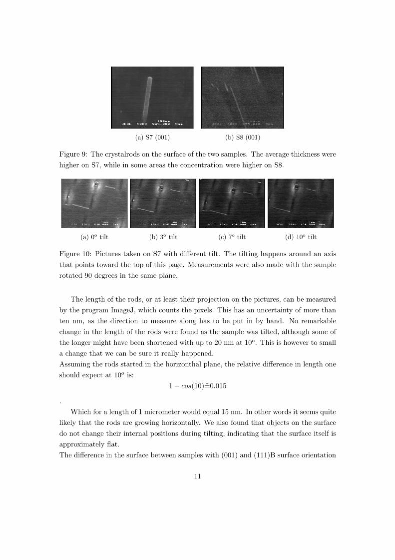
(a) S7 (001) (b) S8 (001)
Figure 9: The crystalrods on the surface of the two samples. The average thickness were
higher on S7, while in some areas the concentration were higher on S8.
(a) 0o tilt (b) 3o tilt (c) 7o tilt (d) 10o tilt
Figure 10: Pictures taken on S7 with different tilt. The tilting happens around an axis
that points toward the top of this page. Measurements were also made with the sample
rotated 90 degrees in the same plane.
The length of the rods, or at least their projection on the pictures, can be measured
by the program ImageJ, which counts the pixels. This has an uncertainty of more than
ten nm, as the direction to measure along has to be put in by hand. No remarkable
change in the length of the rods were found as the sample was tilted, although some of
the longer might have been shortened with up to 20 nm at 10o. This is however to small
a change that we can be sure it really happened.
Assuming the rods started in the horizonthal plane, the relative difference in length one
should expect at 10o is:
1 − cos(10)=0.015
.
Which for a length of 1 micrometer would equal 15 nm. In other words it seems quite
likely that the rods are growing horizontally. We also found that objects on the surface
do not change their internal positions during tilting, indicating that the surface itself is
approximately flat.
The difference in the surface between samples with (001) and (111)B surface orientation
11

might actually be the reason for why ordered growth can only be found on the (001)
surfaces. The cavities that covered part of the surface of the simply annealed samples
in the former section could have shortened the distance of diffusion on samples with
(111)B orientation (recall that the annealing study only used (111)B and no (001)). In
hindsight, or as a subject for future research, it might therefore have been worthwhile to
also have studied the effect of annealing on (001) oriented surfaces. Judging by the sam-
ples which has been subjected to epitaxial growth, the (001) surface would be smoother,
and the particles could have a larger chance of reaching the site of a seedparticle(Notice
though that the only indication that the rods even grew from seedparticles are their
absence in the clipmark).
In a study[16] by Vogel et. al. where chemical beam epitaxy were used in conjunc-
tion with Ag-seedparticles to grow InSb(111)B wires it was found that at temperatures
higher than 380o C the growth rate of a parasitic film on the surface started to approach
the growth rate of the NWs. It’s dubious whether this result is relevant for our samples,
where both epitaxy and catalyst are different, but assuming it holds it could explain
the behaviour of the (111)B samples during growth: The seedparticles could have been
swallowed up by a layer of InAs growing straight on the substrate. In favour of this
hypothesis it can be pointed out, that the cavities we saw were created on (111)B sub-
strates by annealing could have stopped deposited particle’s diffusion across the samples,
causing broad crystal-layer growth.
5 conclusion
Apparently NWs do not form from Cu-seed particles under a molecular beam of InAs.
However highly aligned onedimensional surface crystals did form, and only in areas on
which there had been copper. These were not seen at the lowest growth temperature of
425o C, and neither on the (111)b substrates.
6 acknowledgements
I am very grateful to Jessica Bolinsson for all her help and guidance. Also to Jesper
Nygard who made the project possible, to Nader Payami who taught me to use the SEM
and other facilities. Also to Alexander Whiticar who helped me to get second opinions
on some of the samples, using a different electron microscope. This was of much help at
a time of uncertainty.
12

References
[1] : Erikas Gaidamauskas, Jens Paaske, and Karsten Flensberg: Majorana Bound
States in Two-Channel Time-Reversal-Symmetric Nanowire Systems. Phys. Rev.
Lett. 112, 126402 – Published 25 March 2014
[2] : Fernando Patolsky, Gengfeng Zheng, Charles M. Lieber: NANOWIRE-BASED
BIOSENSORS. JULY 1, 20 06 / ANALYTICAL CHEMISTRY
[3] :Kimberly A Dick, Philippe Caroff, Jessica Bolinsson, Maria E Messing, Jonas Jo-
hansson, Knut Deppert, L Reine Wallenberg and Lars Samuelson: Control of III–V
nanowire crystal structure by growth parameter tuning. Published 22 January 2010
Online at stacks.iop.org/SST/25/024009
[4] : V. G. Dubrovskii, N. V. Sibirev, G. E. Cirlin, J. C. Harmand, and V. M. Ustinov:
Theoretical analysis of the vapor-liquid-solid mechanism of nanowire growth during
molecular beam epitaxy. Phys. Rev. E 73, 021603 – Published 14 February 2006.
[5] : A. Whiticar: Scanning Electron Microscopy Analyses of Ag Catalyzed GaAs
Growth. (2014)
[6] : Karla Hillerich: Copper as Seed Particle Material for InP Nanowires. (Licentiate
Thesis, University of Lund, 2011)
[7] : R. K. Debnath, R. Meijers, T. Richter, T. Stoics, R. Calarco, and H. Luth: Mech-
anism of molecular beam epitaxy growth og GaN nanowires. Appl. Phys. Lett. 90,
123117 (2007)
[8] : E. Hilner, A. Mikkelsen, J. Eriksson, J. N. Andersen, E. Lundgren, A. Zakharov, H.
Yi, and P. Kratzer: Au wetting and nanoparticle stability on GaAs(111)B. Applied
Physics Letters 89, 251912 (2006)
[9] : E. Hilner, E. Lundgren, A. Mikkelsen: Surface structure and morphology of
InAs(111)B with/without gold nanoparticles annealed under arsenic or atomic hy-
drogen flux. Surface Science 604 (2010) 354-360.
[10] : Ann Persson: Epitaxial growth of semiconductor nanowires. Doctoral Thesis.
(2005)
[11] : Donald L. Smith: Thin-Film Deposition: principles and practice. pp. 129-156
(1995)
13

[12] : Linus E. Jensen, Mikael T. Bkork, Soren Jeppesen, Ann I. Persson, B. Jonas
Ohlsson, and Lars Samuelson: Role of Surface Diffusion in Chemical Beam Epitaxy
of InAs Nanowires. (2004)
[13] : Picture taken from: http://spie.org/x37025.xml
[14] : Picture taken from: http://www.wesrch.com/wiki-1054-surface-diffusion-
description-and-equation
[15] :Picture taken from: https://www.physik.uni-kl.de/hillebrands/research/methods/molecular-
beam-epitaxy/
[16] : Alexander T. Vogel, Johannes de Boor, Michael Becker, Joerg V. Wittermann,
Samuel L. Mensah, Peter Werner, and Volker Schmidt: Ag-assisted CBE growth of
ordered InSb nanowire arrays. Nanotechnology 22(2011) 015605(6pp).
[17] : Linus E. Jensen, Mikael T. Bjork, Soren Jeppesen, Ann I. Persson, B. Jonas
Ohlsson, and Lars Samuelson: Role of Surface Diffusion in Chemical Beam Epitaxy
of InAs Nanowires. (2004)
14