COP8 FLASH ISP HANDBOOK-Intro to ISP - Texas Instruments
60
Application Report SNOA082C – May 2004 – Revised May 2004 AN-1150 COP8™ FLASH ISP HANDBOOK—Intro to ISP ..................................................................................................................................................... ABSTRACT This application note describes the COP8™ In System Programming (ISP) Software. ISP method of programming the flash memory are thoroughly discussed. Contents 1 Introduction .................................................................................................................. 3 2 Introduction to ISP—Software Topics .................................................................................... 3 3 ADVANCED ISP—SOFTWARE TOPICS .............................................................................. 13 4 ISP DOWNLOADER ...................................................................................................... 25 Appendix A ....................................................................................................................... 59 List of Figures 1 Block Diagram of ISP....................................................................................................... 4 2 Sample Application Circuit ................................................................................................. 8 3 Flow for the Sequencer Program........................................................................................ 13 4 ISP Boot ROM Interface .................................................................................................. 13 5 COP8 FLASH Memory Layout ........................................................................................... 14 6 MICROWIRE/PLUS Example ............................................................................................ 16 7 MICROWIRE/PLUS Interface Timing, Normal SK Mode, SK Idle Phase being High ............................ 16 8 Parallel Port Connection Diagram....................................................................................... 17 9 MICROWIRE/PLUS Interface Timing, Normal SK Mode, SK Idle Phase being High ............................ 17 10 ISP Command Frame ..................................................................................................... 18 11 Cascade Delay Requirement ............................................................................................ 18 12 Byte Write Waveform (Relative Bytes are Shown) .................................................................... 19 13 Block Write Waveform (Relative Bytes are Shown) .................................................................. 19 14 Page Erase Waveform (Relative Bytes are Shown) .................................................................. 20 15 Mass Erase Waveform (Relative Bytes are Shown) .................................................................. 20 16 The ISP—MICROWIRE Control ......................................................................................... 21 17 The Set PGMTIM Command............................................................................................. 21 18 The PAGE ERASE Command ........................................................................................... 22 19 The MASS_ERASE Command .......................................................................................... 23 20 The READ_BYTE Command ............................................................................................ 23 21 The WRITE_BYTE Command ........................................................................................... 23 22 The Block Write Routine .................................................................................................. 24 23 The Block Read Command .............................................................................................. 24 24 The EXIT Command ...................................................................................................... 25 25 Interfacing the COP8SGR and COP8CBR Microcontrollers ......................................................... 25 26 Flow Chart for the Initialization Routine ................................................................................ 26 COP8, MICROWIRE/PLUS, WATCHDOG are trademarks of Texas Instruments. ICE is a trademark of Intel Corporation. MetaLink is a trademark of dcl_owner. All other trademarks are the property of their respective owners. 1 SNOA082C – May 2004 – Revised May 2004 AN-1150 COP8™ FLASH ISP HANDBOOK—Intro to ISP Submit Documentation Feedback Copyright © 2004, Texas Instruments Incorporated
Transcript of COP8 FLASH ISP HANDBOOK-Intro to ISP - Texas Instruments

Application ReportSNOA082C–May 2004–Revised May 2004
AN-1150 COP8™ FLASH ISP HANDBOOK—Intro to ISP.....................................................................................................................................................
ABSTRACT
This application note describes the COP8™ In System Programming (ISP) Software. ISP method ofprogramming the flash memory are thoroughly discussed.
Contents1 Introduction .................................................................................................................. 32 Introduction to ISP—Software Topics .................................................................................... 33 ADVANCED ISP—SOFTWARE TOPICS .............................................................................. 134 ISP DOWNLOADER ...................................................................................................... 25Appendix A ....................................................................................................................... 59
List of Figures
1 Block Diagram of ISP....................................................................................................... 4
2 Sample Application Circuit ................................................................................................. 8
3 Flow for the Sequencer Program........................................................................................ 13
4 ISP Boot ROM Interface .................................................................................................. 13
5 COP8 FLASH Memory Layout........................................................................................... 14
6 MICROWIRE/PLUS Example............................................................................................ 16
7 MICROWIRE/PLUS Interface Timing, Normal SK Mode, SK Idle Phase being High ............................ 16
8 Parallel Port Connection Diagram....................................................................................... 17
9 MICROWIRE/PLUS Interface Timing, Normal SK Mode, SK Idle Phase being High ............................ 17
10 ISP Command Frame..................................................................................................... 18
11 Cascade Delay Requirement ............................................................................................ 18
12 Byte Write Waveform (Relative Bytes are Shown).................................................................... 19
13 Block Write Waveform (Relative Bytes are Shown) .................................................................. 19
14 Page Erase Waveform (Relative Bytes are Shown) .................................................................. 20
15 Mass Erase Waveform (Relative Bytes are Shown) .................................................................. 20
16 The ISP—MICROWIRE Control ......................................................................................... 21
17 The Set PGMTIM Command............................................................................................. 21
18 The PAGE ERASE Command........................................................................................... 22
19 The MASS_ERASE Command .......................................................................................... 23
20 The READ_BYTE Command ............................................................................................ 23
21 The WRITE_BYTE Command ........................................................................................... 23
22 The Block Write Routine.................................................................................................. 24
23 The Block Read Command .............................................................................................. 24
24 The EXIT Command ...................................................................................................... 25
25 Interfacing the COP8SGR and COP8CBR Microcontrollers......................................................... 25
26 Flow Chart for the Initialization Routine ................................................................................ 26
COP8, MICROWIRE/PLUS, WATCHDOG are trademarks of Texas Instruments.ICE is a trademark of Intel Corporation.MetaLink is a trademark of dcl_owner.All other trademarks are the property of their respective owners.
1SNOA082C–May 2004–Revised May 2004 AN-1150 COP8™ FLASH ISP HANDBOOK—Intro to ISPSubmit Documentation Feedback
Copyright © 2004, Texas Instruments Incorporated
www.ti.com
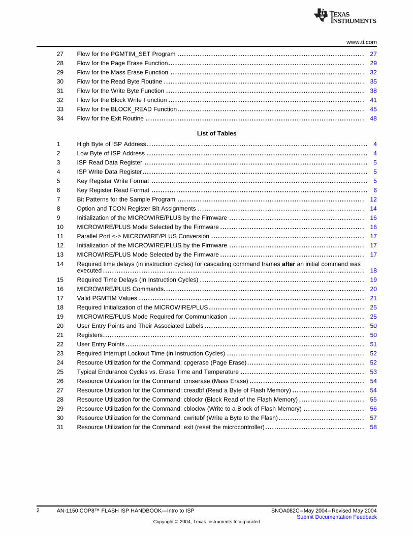
27 Flow for the PGMTIM_SET Program ................................................................................... 27
28 Flow for the Page Erase Function....................................................................................... 29
29 Flow for the Mass Erase Function ...................................................................................... 32
30 Flow for the Read Byte Routine ......................................................................................... 35
31 Flow for the Write Byte Function ........................................................................................ 38
32 Flow for the Block Write Function ....................................................................................... 41
33 Flow for the BLOCK_READ Function................................................................................... 45
34 Flow for the Exit Routine ................................................................................................. 48
List of Tables
1 High Byte of ISP Address.................................................................................................. 4
2 Low Byte of ISP Address .................................................................................................. 4
3 ISP Read Data Register ................................................................................................... 5
4 ISP Write Data Register.................................................................................................... 5
5 Key Register Write Format ................................................................................................ 5
6 Key Register Read Format ................................................................................................ 6
7 Bit Patterns for the Sample Program ................................................................................... 12
8 Option and TCON Register Bit Assignments .......................................................................... 14
9 Initialization of the MICROWIRE/PLUS by the Firmware ............................................................ 16
10 MICROWIRE/PLUS Mode Selected by the Firmware ................................................................ 16
11 Parallel Port <-> MICROWIRE/PLUS Conversion .................................................................... 17
12 Initialization of the MICROWIRE/PLUS by the Firmware ............................................................ 17
13 MICROWIRE/PLUS Mode Selected by the Firmware ................................................................ 17
14 Required time delays (in instruction cycles) for cascading command frames after an initial command wasexecuted .................................................................................................................... 18
15 Required Time Delays (In Instruction Cycles) ......................................................................... 19
16 MICROWIRE/PLUS Commands......................................................................................... 20
17 Valid PGMTIM Values .................................................................................................... 21
18 Required Initialization of the MICROWIRE/PLUS ..................................................................... 25
19 MICROWIRE/PLUS Mode Required for Communication ............................................................ 25
20 User Entry Points and Their Associated Labels....................................................................... 50
21 Registers.................................................................................................................... 50
22 User Entry Points .......................................................................................................... 51
23 Required Interrupt Lockout Time (in Instruction Cycles) ............................................................. 52
24 Resource Utilization for the Command: cpgerase (Page Erase).................................................... 52
25 Typical Endurance Cycles vs. Erase Time and Temperature ....................................................... 53
26 Resource Utilization for the Command: cmserase (Mass Erase) ................................................... 54
27 Resource Utilization for the Command: creadbf (Read a Byte of Flash Memory) ................................ 54
28 Resource Utilization for the Command: cblockr (Block Read of the Flash Memory) ............................. 55
29 Resource Utilization for the Command: cblockw (Write to a Block of Flash Memory) ........................... 56
30 Resource Utilization for the Command: cwritebf (Write a Byte to the Flash) ...................................... 57
31 Resource Utilization for the Command: exit (reset the microcontroller)............................................ 58
2 AN-1150 COP8™ FLASH ISP HANDBOOK—Intro to ISP SNOA082C–May 2004–Revised May 2004Submit Documentation Feedback
Copyright © 2004, Texas Instruments Incorporated

www.ti.com Introduction
1 Introduction
In-System Programming (ISP) allows the user to re-program a microcontroller without physical removal.The COP8™ ISP Software allows the user to program the flash memory in three ways. A user maychoose to program the flash memory by using the Boot ROM's user support portion, the MetaLink™support portion (via the Flash emulator module) or the MICROWIRE/PLUS™ support portion. The use of auser and/or MICROWIRE/PLUS™ support portions are fully documented and their requirements arespecified. Other application notes that relate to the COP8™ FLASH ISP software include AN-1151(Parallel Port Programming Adapter), AN-1152 (FLASHDOS Programmer Source), AN-1153 (Virtual E2
Guide), AN-1154 (FLASHWIN Programmer’s Guide) and AN-1161 (FLASHDOS Programmer’s Guide).
2 Introduction to ISP—Software Topics
The Flash Family provides the capability to program the Program Memory while installed in an applicationboard. This feature is called In System Programming (ISP). It provides a means of ISP by using theMICROWIRE/PLUS™, or the user can provide his own, customized ISP routine. This customized routinemay use any of the capabilities of the device, such as USART, parallel port, etc. The factory installed ISPuses only the MICROWIRE/PLUS™ port.
2.1 Functional Description
The organization of the ISP feature consists of the user flash program memory, the factory Boot ROM,and some registers dedicated to performing the ISP function. See Figure 1 for a simplified block diagram.The factory installed ISP that uses MICROWIRE/PLUS is located in the Boot ROM. The size of the BootROM is 1K bytes and also includes the ICE™ monitor code. If a user chooses to write his own ISProutine, it must be located in the flash program memory.
In the next section, ADVANCED ISP SOFTWARE TOPICS, a discussion regarding the FLEX bit ispresented. The FLEX bit controls whether the device exits RESET executing from the flash memory or theBoot ROM. The user must program this Configuration Register bit as appropriate for the application. In theerased state, the FLEX bit = 0 and the device will power-up executing from Boot ROM. When FLEX = 0,this assumes that either the MICROWIRE/PLUS™ ISP routine or external programming is being used toprogram the device. If using the MICROWIRE/PLUS™ ISP routine, the software in the Boot ROM willmonitor the MICROWIRE/PLUS™ for commands to program the flash memory. When programming theflash program memory is complete, the FLEX bit will have to be programmed to a 1 and the device willhave to be reset, either by pulling external Reset to ground or by software, before execution from flashprogram memory will occur.
If FLEX = 1, upon exiting Reset, the device will begin executing from location 0000 in the flash programmemory. The assumption here, is that either the application is not using ISP, but is usingMICROWIRE/PLUS™ ISP by jumping to it within the application code or is using a customized ISProutine. If a customized ISP routine is being used, then it must be programmed into the flash memory bymeans of MICROWIRE/PLUS™ ISP or external programming as described in the preceding paragraph.
3SNOA082C–May 2004–Revised May 2004 AN-1150 COP8™ FLASH ISP HANDBOOK—Intro to ISPSubmit Documentation Feedback
Copyright © 2004, Texas Instruments Incorporated

Introduction to ISP—Software Topics www.ti.com
Figure 1. Block Diagram of ISP
2.1.1 REGISTERS
There are six registers required to support ISP: Address Register Hi byte (ISPADHI), Address RegisterLow byte (ISPADLO), Read Data Register (ISPRD), Write Data Register (ISPWR), Write Timing Register(PGMTIM), and the Control Register (ISPCNTRL).
2.1.1.1 ISP Address Registers
The address registers (ISPADHI and ISPADLO) are used to specify the address of the byte of data beingwritten or read. For page erase operations, the address of the beginning of the page should be loaded.When reading the Option register, FFFF should be placed into the address registers. Registers ISPADHIand ISPADLO are cleared to 00 on Reset. These registers can be loaded from either flash programmemory or Boot ROM and must be maintained for the entire duration of the operation.
Table 1. High Byte of ISP Address
ISPADHI
Bit 7 Bit 6 Bit 5 Bit 4 Bit 3 Bit 2 Bit 1 Bit 0
Addr Addr Addr Addr Addr Addr Addr Addr15 14 13 12 11 10 9 8
Table 2. Low Byte of ISP Address
ISPADLO
Bit 7 Bit 6 Bit 5 Bit 4 Bit 3 Bit 2 Bit 1 Bit 0
Addr Addr Addr Addr Addr Addr Addr Addr7 6 5 4 3 2 1 0
2.1.1.2 ISP Read Data Register
The Read Data Register (ISPRD) contains the value read back from a read operation. This register can beaccessed from either flash program memory or Boot ROM. This register is undefined on Reset. CAUTION:Read/Modify/Write instructions are not allowed to be used on this register.
4 AN-1150 COP8™ FLASH ISP HANDBOOK—Intro to ISP SNOA082C–May 2004–Revised May 2004Submit Documentation Feedback
Copyright © 2004, Texas Instruments Incorporated

www.ti.com Introduction to ISP—Software Topics
Table 3. ISP Read Data Register
ISPRD
Bit 7 Bit 6 Bit 5 Bit 4 Bit 3 Bit 2 Bit 1 Bit 0
Bit7 Bit6 Bit5 Bit4 Bit3 Bit2 Bit1 Bit0
2.1.1.3 ISP Write Data Register
The Write Timing Register (PGMTIM) is used to control the width of the timing pulses for write and eraseoperations. The value to be written into this register is dependent on the frequency of CKI and is shown inTable 17. This register must be written before any write or erase operation can take place. It only needs tobe loaded once, for each value of CKI frequency. If a dedicated E2 block exists on the device and it's inthe process of writing, this register should not be changed until the E2 write cycle is completed.
Table 4. ISP Write Data Register
ISPWR
Bit 7 Bit 6 Bit 5 Bit 4 Bit 3 Bit 2 Bit 1 Bit 0
Bit7 Bit6 Bit5 Bit4 Bit3 Bit2 Bit1 Bit0
2.1.1.4 ISP Write Timing Register
The Write Timing Register (PGMTIM) is used to control the width of the timing pulses for write and eraseoperations. The value to be written into this register is dependent on the frequency of CKI and is shown inTable 17. This register must be written before any write or erase operation can take place. It only needs tobe loaded once, for each value of CKI frequency. This register can be loaded from either flash programmemory or Boot ROM and must be maintained for the entire duration of the operation. If a dedicated E2
block exists on the device and it's in the process of writing, this register should not be changed until the E2
write cycle is completed.
2.1.2 MANEUVERING BACK AND FORTH BETWEEN FLASH MEMORY AND BOOT ROM
When using ISP, at some point, it will be necessary to maneuver between the flash program memory andthe Boot ROM, even when using customized ISP routines. This is because it's not possible to executefrom the flash program memory while it's being programmed.
The JSRB instruction is used to Jump to the Boot ROM. Refer to the COP8™ Flash Family User Manualfor specific details on the operation of this instruction. The JSRB instruction must be used in conjunctionwith the Key register. This is to prevent jumping to the Boot ROM in the event of run-away software. Forthe JSRB instruction to actually jump to the Boot ROM, the Key bit must be set. This is done by writing thevalue shown in Table 5 to the Key register. The Key is a 6-bit key and, if the key matches, the KEY bit willbe set for 8 instruction cycles. The JSRB instruction must be executed while the KEY bit is set. If the KEYdoes not match, then the KEY bit will not be set and the JSRB will jump to the specified location in theflash memory. In emulation mode, if a breakpoint is encountered while the KEY is set, the counter thatcounts the instruction cycles will be frozen until the breakpoint condition is cleared. The Key register is amemory mapped register. Its format when writing is shown in Table 5. Its format when reading is shown inTable 6. In normal operation, it is not necessary to test the KEY bit before using the JSRB instruction. Thereading of the Key register is primarily used for testing. Also, located in the Key register is a bit calledEFLEX. This bit is also used for testing.
Table 5. Key Register Write Format
KEY when Writing
Bit 7 Bit 6 Bit 5 Bit 4 Bit 3 Bit 2 Bit 1 Bit 0
1 0 0 1 1 0 X X
5SNOA082C–May 2004–Revised May 2004 AN-1150 COP8™ FLASH ISP HANDBOOK—Intro to ISPSubmit Documentation Feedback
Copyright © 2004, Texas Instruments Incorporated

Introduction to ISP—Software Topics www.ti.com
Bits 7–2:— Key value that must be written to set the KEY bit.
Bits 1–0:—Don't care.
Table 6. Key Register Read Format
KEY when Reading
Bit 7 Bit 6 Bit 5 Bit 4 Bit 3 Bit 2 Bit 1 Bit 0
0 0 0 0 0 0 EFLEX KEY
R R R R R R R R
Bits 7–2:—Read back as 0.
EFLEX (FLASH EXECUTION):—This is the bit that actually controls whether program execution occursfrom flash memory or Boot ROM. It uses data from the Option Register bit in combination with otherlogic controlled by the JSRB instruction, and the G6 hardware override. When EFLEX = 1,execution is from the flash program memory. When EFLEX = 0, program execution occurs from theBoot ROM. This is a Read Only bit.
KEY:— This is the state of the Key. If it is set, it indicates that a valid key was written to the Key registerand the JSRB instruction will jump correctly to the Boot ROM. If it's cleared, the key is not valid andthe JSRB instruction will jump to the specified address in flash program memory. Once set, thehardware will clear it to 0 after 8 instruction cycles. This is used primarily for testing. This is a ReadOnly bit.
2.1.3 FORCED EXECUTION FROM BOOT ROM
When the user is developing his own ISP routine, he may encounter code lockups due to mistakes in hissoftware. There is a hardware method to get out of these lockups and force execution from the BootROM's MICROWIRE/PLUS routine, so that the customer can erase his flash code and start over. Themethod to force this condition is to drive the G6 pin to high voltage (2X VCC) and activate Reset. As a notefor user of the parallel printer port connects, it is advisable that the user remove the G6 line from the PCwhen applying high voltage. The voltage may be high enough to permanently damage the PC parallel portlogic circuits. The high voltage condition on G6 must be held for at least 3 instruction cycles longer thanReset is active. This special condition will start execution from location 0000 in the Boot ROM where theuser can input the appropriate commands, using MICROWIRE/PLUS™, to erase the flash programmemory and reprogram it.
2.1.4 RETURN TO FLASH WITHOUT HARDWARE RESET
After programming the entire program memory, including options (and setting the FLEX bit in the OptionRegister), it is necessary to exit the Boot ROM and return to the flash program memory for programexecution. This can be accomplished through the use of the MICROWIRE/PLUS™ ISP Exit command asdescribed later.
2.1.5 MICROWIRE/PLUS ISP COMMANDS
The MICROWIRE/PLUS™ ISP will support the following features and commands:
• Read a byte from a specified address.
• Write a byte from a specified address.
• Erase a page at a specified address.
• Erase the entire flash program memory (mass erase).
• Read multiple bytes starting at a specified address.
• Write multiple bytes starting at a specified address.
• Read Option register.
• Exit ISP by resetting the device and return execution to flash program memory if the FLEX bit is set inthe Option Register.
6 AN-1150 COP8™ FLASH ISP HANDBOOK—Intro to ISP SNOA082C–May 2004–Revised May 2004Submit Documentation Feedback
Copyright © 2004, Texas Instruments Incorporated

www.ti.com Introduction to ISP—Software Topics
2.1.6 VIRTUAL E2 COMMANDS
The following commands will support transferring blocks of data from RAM to flash program memory, andvice-versa.
• Erase a page of flash memory at a specified address.
• Copy a block of data from RAM into flash program memory.
• Copy a block of data from program flash memory to RAM.
2.1.7 SAMPLE PROGRAM: A Light Sequencer.
Since we have completed our introduction to Flash Family device, lets begin to work on our sampleapplication program.
The goal of this section is to familiarize the user with the following:
1. Writing and saving a program for the COP8™ Flash Family devices
2. Using the MICROWIRE/PLUS™ flash command: Set PGMTIM (write timing register)
3. Using the internal flash command: cwritebf (write a byte to the flash)
4. Using the internal flash command: creadbf (read a byte from the flash)
5. Using the internal/ MICROWIRE/PLUS™ flash command: EXIT (reset the microcontroller).
We will achieve the above commands by using the FLASHWIN Programmer’s Guide. See ApplicationNote–1154 for additional information.
2.1.7.1 Description of the Sample Application Program
The goal of the sample program is to teach the user the basics of using the COP8™ flash family devices.The schematic in Figure 2 shows the circuit we are going to use. We will be attaching 8 LEDs, Each LEDwill be connected in such a way as to sink current from the microcontroller. The cathode (long leg of theLED) will be connected toward the COP8™ Flash Family devices. The short leg of the LED (anode) will beconnected through a resistor toward the VCC power supply.
7SNOA082C–May 2004–Revised May 2004 AN-1150 COP8™ FLASH ISP HANDBOOK—Intro to ISPSubmit Documentation Feedback
Copyright © 2004, Texas Instruments Incorporated

Introduction to ISP—Software Topics www.ti.com
Figure 2. Sample Application Circuit
2.1.7.2 Writing the Program
We will begin first by writing the program. Launch the Windows 95 Editor by going to the taskbar andclicking on the Start button. Then click on Run. At the Run dialog Open window type in the Openfieldedit. Type in exactly as is listed in Example 1. When done, Click on File and then Save. At the newdialog window type in c:\asm\sequencer.asm (where asm is the directory in which the assembler isinstalled in). When done, click on File and then click on Exit.
Example 1. Sample Application Code (sequence.asm)
; Program: Sequence.asm; Purpose: Demonstrate the use of flash routines; Date: 02/5/00.INCLD COP8CBR.INC ;INCLUDE FILE FOR THE COP8CBRcreadbf = 011 ; Entry point for the read byte of flash commandcwritebf = 014 ; Entry point for the write byte of flash commandexit = 062 ; Entry point for Resetting the microcontroller.sect data,reg,abs=0xF4 ;FOR RAM STORAGE AREALED_BITPOS:.DSB 1 ;STORAGE FOR THE LED POSITIONDELAY_NUM: .DSB 1 ;STORAGE FOR THE NUMBER OF DELAYS.sect code,rom,abs=0 ;BEGINNING CODE SPACE.org 0 ;START AT LOCATION 0MAIN:
8 AN-1150 COP8™ FLASH ISP HANDBOOK—Intro to ISP SNOA082C–May 2004–Revised May 2004Submit Documentation Feedback
Copyright © 2004, Texas Instruments Incorporated

www.ti.com Introduction to ISP—Software Topics
Example 1. Sample Application Code (sequence.asm) (continued)
LD S,#000RBIT 2,PORTLC ;USE PORTL.2 AS AN INPUTSBIT 2,PORTLD ;CAUSE PORTL.2 TO BE AN INPUT WITH PULL-UPLD PGMTIM,#07B ;FOR A 10MHZ CLOCKLD ISPADHI,#000 ;LOAD THE HIGH BYTE ADDRESSLD ISPADLO,#0A0 ;LOAD THE LOW BYTE ADDRESSLD ISPWR,#080 ;FOR LED POSITION 10000000LD ISPKEY,#098 ;LOAD THE KEYJSRB cwritebf ;CALL THE ROUTINELD ISPADLO,#0A1 ;LOAD THE LOW BYTE ADDRESSLD ISPWR,#040 ;FOR LED POSITION 01000000LD ISPKEY,#098 ;LOAD THE KEYJSRB cwritebf ;CALL THE ROUTINELD ISPWR,#020 ;FOR LED POSITION 00100000LD ISPADLO,#0A2 ;LOAD THE LOW BYTE ADDRESSLD ISPKEY,#098 ;LOAD THE KEYJSRB cwritebf ;CALL THE ROUTINELD ISPWR,#010 ;FOR LED POSITION 00010000LD ISPADLO,#0A3 ;LOAD THE LOW BYTE ADDRESSLD ISPKEY,#098 ;LOAD THE KEYJSRB cwritebf ;CALL THE ROUTINELD ISPWR,#008 ; FOR LED POSITION 00001000LD ISPADLO,#0A4 ; LOAD THE LOW BYTE ADDRESSLD ISPKEY,#098 ; LOAD THE KEYJSRB cwritebf ; CALL THE ROUTINELD ISPWR,#004 ; FOR LED POSITION 00000100LD ISPADLO,#0A5 ; LOAD THE LOW BYTE ADDRESSLD ISPKEY,#098 ; LOAD THE KEYJSRB cwritebf ; CALL THE ROUTINELD ISPWR,#002 ; FOR LED POSITION 00000010LD ISPADLO,#0A6 ; LOAD THE LOW BYTE ADDRESSLD ISPKEY,#098 ; LOAD THE KEYJSRB cwritebf ; CALL THE ROUTINELD ISPWR,#001 ; FOR LED POSITION 00000001LD ISPADLO,#0A7 ; LOAD THE LOW BYTE ADDRESSLD ISPKEY,#098 ; LOAD THE KEYJSRB cwritebf ; CALL THE ROUTINELOOP: ; BEGINNING OF THE LOOPLD LED_BITPOS,#0A0 ; POSITION IS INITIALIZED TO #0A0SEQUENCE: ; BEGINING OF THE SEQUENCEJSR DELAY ; JUMP TO THE DELAY ROUTINELD A,LED_BITPOS ; GET THE BIT POSITIONX A,ISPADLO ; SWAP IT WITH THE ISP LOW ADDRESS BYTELD ISPKEY,#098 ; LOAD THE KEYJSRB creadbf ; CALL THE ROUTINELD A,ISPRD ; LOAD THE RESULTS INTO THE ACCUMULATORX A,PORTD ; SWAP IT WITH PORTDLD A,LED_BITPOS ; LOAD THE LED_BITPOS VARIABLE
; ROTATE THROUGH THE BIT POSITIONSINC A ; INCREMENT THE ACCUMULATORX A,LED_BITPOS ; SWAP IT WITH THE LED_BITPOSIFEQ A,#0A7 ; STOP AT THE EIGHTH BIT POSITION SHIFTJP LOOP ; RETURNING TO THE MAIN LOOPJP SEQUENCE ; RETURN TO THE MAIL LOOP SEQUENCEDELAY:LD DELAY_NUM,#0FF ; CREATE 256 NOPSDELAY_LOOP: ; THE DELAY ROUTINENOP ; CREATE A 1 CYCLE DELAYNOP ; CREATE A 1 CYCLE DELAYDRSZ DELAY_NUM ; COUNT DOWN UNTIL ZEROJP DELAY_LOOP ; OTHERWISE JUST JUMP INTO THE DELAYRETIFBIT 2,PORTLP ; DETECT IF THE SWITCH IS OFFJP NEXT2 ; IF OFF THEN GOTO NEXT COMMAND
9SNOA082C–May 2004–Revised May 2004 AN-1150 COP8™ FLASH ISP HANDBOOK—Intro to ISPSubmit Documentation Feedback
Copyright © 2004, Texas Instruments Incorporated
Introduction to ISP—Software Topics www.ti.com
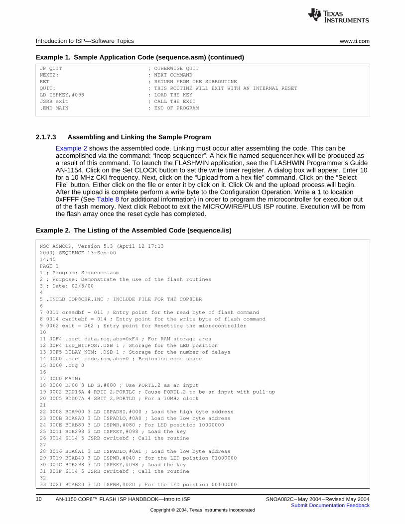
Example 1. Sample Application Code (sequence.asm) (continued)
JP QUIT ; OTHERWISE QUITNEXT2: ; NEXT COMMANDRET ; RETURN FROM THE SUBROUTINEQUIT: ; THIS ROUTINE WILL EXIT WITH AN INTERNAL RESETLD ISPKEY,#098 ; LOAD THE KEYJSRB exit ; CALL THE EXIT.END MAIN ; END OF PROGRAM
2.1.7.3 Assembling and Linking the Sample Program
Example 2 shows the assembled code. Linking must occur after assembling the code. This can beaccomplished via the command: “lncop sequencer”. A hex file named sequencer.hex will be produced asa result of this command. To launch the FLASHWIN application, see the FLASHWIN Programmer’s GuideAN-1154. Click on the Set CLOCK button to set the write timer register. A dialog box will appear. Enter 10for a 10 MHz CKI frequency. Next, click on the “Upload from a hex file” command. Click on the “SelectFile” button. Either click on the file or enter it by click on it. Click Ok and the upload process will begin.After the upload is complete perform a write byte to the Configuration Operation. Write a 1 to location0xFFFF (See Table 8 for additional information) in order to program the microcontroller for execution outof the flash memory. Next click Reboot to exit the MICROWIRE/PLUS ISP routine. Execution will be fromthe flash array once the reset cycle has completed.
Example 2. The Listing of the Assembled Code (sequence.lis)
NSC ASMCOP, Version 5.3 (April 12 17:132000) SEQUENCE 13-Sep-0014:45PAGE 11 ; Program: Sequence.asm2 ; Purpose: Demonstrate the use of the flash routines3 ; Date: 02/5/0045 .INCLD COP8CBR.INC ; INCLUDE FILE FOR THE COP8CBR67 0011 creadbf = 011 ; Entry point for the read byte of flash command8 0014 cwritebf = 014 ; Entry point for the write byte of flash command9 0062 exit = 062 ; Entry point for Resetting the microcontroller1011 00F4 .sect data,reg,abs=0xF4 ; For RAM storage area12 00F4 LED_BITPOS:.DSB 1 ; Storage for the LED position13 00F5 DELAY_NUM: .DSB 1 ; Storage for the number of delays14 0000 .sect code,rom,abs=0 ; Beginning code space15 0000 .org 01617 0000 MAIN:18 0000 DF00 3 LD S,#000 ; Use PORTL.2 as an input19 0002 BDD16A 4 RBIT 2,PORTLC ; Cause PORTL.2 to be an input with pull-up20 0005 BDD07A 4 SBIT 2,PORTLD ; For a 10MHz clock2122 0008 BCA900 3 LD ISPADHI,#000 ; Load the high byte address23 000B BCA8A0 3 LD ISPADLO,#0A0 ; Load the low byte address24 000E BCAB80 3 LD ISPWR,#080 ; For LED position 1000000025 0011 BCE298 3 LD ISPKEY,#098 ; Load the key26 0014 6114 5 JSRB cwritebf ; Call the routine2728 0016 BCA8A1 3 LD ISPADLO,#0A1 ; Load the low byte address29 0019 BCAB40 3 LD ISPWR,#040 ; for the LED poistion 0100000030 001C BCE298 3 LD ISPKEY,#098 ; Load the key31 001F 6114 5 JSRB cwritebf ; Call the routine3233 0021 BCAB20 3 LD ISPWR,#020 ; For the LED poistion 00100000
10 AN-1150 COP8™ FLASH ISP HANDBOOK—Intro to ISP SNOA082C–May 2004–Revised May 2004Submit Documentation Feedback
Copyright © 2004, Texas Instruments Incorporated

www.ti.com Introduction to ISP—Software Topics
Example 2. The Listing of the Assembled Code (sequence.lis) (continued)
34 0024 BCA8A2 3 LD ISPADLO,#0A2 ; Load the low byte address35 0027 BCE298 3 LD ISPKEY,#098 ; Load the key36 002A 6114 5 JSRB cwritebf ; Call the routine3738 002C BCAB10 3 LD ISPWR,#010 ; For the LED poistion 0001000039 002F BCA8A3 3 LD ISPADLO,#0A3 ; Load the low byte address40 0032 BCE298 3 LD ISPKEY,#098 ; Load the key41 0035 6114 5 JSRB cwritebf ; Call the routine4243 0037 BCAB08 3 LD ISPWR,#008 ; For the LED poistion 0000100044 003A BCA8A4 3 LD ISPADLO,#0A4 ; Load the low byte address45 003D BCE298 3 LD ISPKEY,#098 ; Load the key46 0040 6114 5 JSRB cwritebf ; Call the routine4748 0042 BCAB04 3 LD ISPWR,#004 ; For the LED poistion 0000010049 0045 BCA8A5 3 LD ISPADLO,#0A5 ; Load the low byte address50 0048 BCE298 3 LD ISPKEY,#098 ; Load the key51 004B 6114 5 JSRB cwritebf ; Call the routine5253 004D BCAB02 3 LD ISPWR,#002 ; For the LED poistion 0000010054 0050 BCA8A6 3 LD ISPADLO,#0A6 ; Load the low byte address55 0053 BCE298 3 LD ISPKEY,#098 ; Load the key56 0056 6114 5 JSRB cwritebf ; Call the routineNSC ASMCOP, Version 5.3 (April 12 17:132000) SEQUENCE 13-Sep-0014:45PAGE 25758 0058 BCAB01 3 LD ISPWR,#001 ; For the LED poistion 0000010059 005B BCA8A7 3 LD ISPADLO,#0A7 ; Load the low byte address60 005E BCE298 3 LD ISPKEY,#098 ; Load the key61 0061 6114 5 JSRB cwritebf ; Call the routine6263 0063 LOOP: ; Beginning of the Loop64 0063 D4A0 3 LD LED_BITPOS,#0A0 ; Position is initialized to #0A06566 0065 SEQUENCE: ; Beginning of the sequence67 0065 307D 5 JSR DELAY ; Jump to the delay routine68 0067 9DF4 3 LD A,LED_BITPOS ; Get the bit positon69 0069 9CA8 3 X A,ISPADLO ; Swap it with the ISP low address byte70 006B BCE298 3 LD ISPKEY,#098 ; Load the key71 006E 6111 5 JSRB creadbf ; Call the routine72 0070 9DAA 3 LD A,ISPRD ; Load the results into the accumulator73 0072 9CDC 3 X A,PORTD ; Swap it with PORTD7475 0074 9DF4 3 LD A,LED_BITPOS ; Load the LED_BITPOS variable7677 ; Rotate through the bit positions78 0076 8A 1 INC A ; Increment the accumulator7980 0077 9CF4 3 X A,LED_BITPOS ; Swap it with the LED_BITPOS8182 0079 92A7 2 IFEQ A,#0A7 ; Stop at the eighth bit position shift83 007B E7 3 JP LOOP ; Returning to the main loop84 007C E8 3 JP SEQUENCE ; Return to the main loop sequence8586 007D DELAY:87 007D D5FF 3 LD DELAY_NUM,#0FF ; Create 256 NOPs88 007F DELAY_LOOP: ; The delay routine89 007F B8 1 NOP ; Create a 1 cycle delay90 0080 B8 1 NOP ; Create a 1 cycle delay91 0081 C5 3 DRSZ DELAY_NUM ; Count down until zero92 0082 FC 3 JP DELAY_LOOP ; Otherwise just jump into the delay93 0083 8E 5 RET
11SNOA082C–May 2004–Revised May 2004 AN-1150 COP8™ FLASH ISP HANDBOOK—Intro to ISPSubmit Documentation Feedback
Copyright © 2004, Texas Instruments Incorporated

Introduction to ISP—Software Topics www.ti.com
Example 2. The Listing of the Assembled Code (sequence.lis) (continued)
94 0084 BDD272 4 IFBIT 2,PORTLP ; Detect if the switch is off95 0087 01 3 JP NEXT2 ; If off then goto next command96 0088 01 3 JP QUIT ; Otherwise quit97 0089 NEXT2: ; Next command98 0089 8E 5 RET ; Return from the subroutine99100 008A QUIT: ; This routine will exit with an internal reset101 008A BCE298 3 LD ISPKEY,#098 ; Load the key102 008D 6162 5 JSRB exit ; Call the exit103 008F .END MAIN ; End of program**** Errors: 0, Warnings: 0Checksum: 0x543BByte Count: 0x008F (143)Input File: c:\nsc\sequence.asmOutput File: c:\nsc\sequence.objMemory Model: LargeChip: 8CBR
2.1.7.4 1.8.4 Analysis of the Program
The best way to understand a program is to cut it apart line by line. Lines 14-53 shows how to use thefunction cwritebf (customer write byte). They also show the correct calling format and usage of the JSRBinstruction. Loading the KEY register bit is also shown in the code sample. The code will write the bitpatterns listed in Table 7 to the flash memory.
Lines 66-86 makes up the main calling routine. The code will use the creadbf function to read flashmemory. Lines 92-104 makes up the delay and detect_exit routine. Lines 106-109 makes up the exitroutine. The exit routine calls the reset function and will cause the microcontroller to reset.
The flow to this program is represented in Figure 3.
Table 7. Bit Patterns for the Sample Program
Sequence # Sequence Pattern
1 1 0 0 0 0 0 0 0
2 0 1 0 0 0 0 0 0
3 0 0 1 0 0 0 0 0
4 0 0 0 1 0 0 0 0
5 0 0 0 0 1 0 0 0
6 0 0 0 0 0 1 0 0
7 0 0 0 0 0 0 1 0
8 0 0 0 0 0 0 0 1
12 AN-1150 COP8™ FLASH ISP HANDBOOK—Intro to ISP SNOA082C–May 2004–Revised May 2004Submit Documentation Feedback
Copyright © 2004, Texas Instruments Incorporated

www.ti.com ADVANCED ISP—SOFTWARE TOPICS
Figure 3. Flow for the Sequencer Program
3 ADVANCED ISP—SOFTWARE TOPICS
3.1 IN SYSTEM PROGRAMMING (ISP) SUPPORT BLOCKS
The Flash Family's Boot ROM consists of three main blocks: The user support portion, the MetaLinksupport portion and the MICROWIRE/PLUS support portion. Figure 4 shows the relative organization ofthese support blocks. Each command portion is both independent and self contained. The entire BootROM is 1 Kbytes. This document assumes that the reader is fluent in the use of MICROWIRE/PLUS andits transmission protocol. For reference please refer the MICROWIRE/PLUS section of the Flash Familydatasheet.
Figure 4. ISP Boot ROM Interface
3.2 Boot ROM Memory Layout
Figure 5 shows how the Boot ROM is organized. FLEX is a hardware bit that controls whether programexecution occurs from flash memory of Boot_ROM. It uses data from the Option register. When the FLEXbit option register=1, execution is from the flash program memory. When bit FLEX=0, program executionoccurs from the Boot ROM.
13SNOA082C–May 2004–Revised May 2004 AN-1150 COP8™ FLASH ISP HANDBOOK—Intro to ISPSubmit Documentation Feedback
Copyright © 2004, Texas Instruments Incorporated

ADVANCED ISP—SOFTWARE TOPICS www.ti.com
Figure 5. COP8 FLASH Memory Layout
3.3 PROGRAMMABLE OPTIONS DESCRIPTION
The programmable configuration options for this device are listed below.
• Program Memory Security
• Watchdog feature
• Halt Enable feature
• Power-up execution feature
The options will be stored in the highest location in program memory. This location will be called theOption Register. For devices with 32K of Program Memory, the options are stored at location 7FFF. For16K devices, they will be stored at 3FFF, for 8K devices 1FFF, and for 4K devices 0FFF, however theOption Register can always be accessed by referencing Flash address FFFF. The options areprogrammed with either external programming or ISP. The location must be erased before programming.The user must not store instructions in the Option register location. If the software tries to execute fromthe Option register, 00 data will be returned to the instruction register and the device will execute theSoftware Trap.
3.4 OPTION REGISTER BIT ASSIGNMENTS
The format of the Option Register bit locations are shown in Table 8.
Table 8. Option and TCON Register Bit Assignments
Option Register
Bit 7 Bit 6 Bit 5 Bit 4 Bit 3 Bit 2 Bit 1 Bit 0
Reserved Reserved SEC Reserved Reserved WD HALT FLEX
Bit 7 -— Reserved
Bit 6 -— Reserved
Bit 5 -— SEC - Security bit=1 Security enabled=0 Security disabled
Bits 4,3 -— Reserved
Bit 2 -— WD - Watchdog=1 Watchdog feature is disabled with G1 being a standard I/O.=0 Watchdog feature is enabled to G1 output with weak pull-up enabled when output is not valid.
14 AN-1150 COP8™ FLASH ISP HANDBOOK—Intro to ISP SNOA082C–May 2004–Revised May 2004Submit Documentation Feedback
Copyright © 2004, Texas Instruments Incorporated

www.ti.com ADVANCED ISP—SOFTWARE TOPICS
Bit 1 -— HALT - Halt Enable=1 Halt mode is disabled=0 Halt mode is enabled
Bit 0 -— FLEX - Flash execution=1 Execute from Flash program memory upon exiting Reset=0 Execute from Boot ROM upon exiting Reset
3.5 SECURITY
The device has a security feature, when enabled, it prevents reading, writing, and page erases of the flashprogram memory. Bit-5 in the Option register determines whether security is enabled or disabled. If thesecurity option is disabled, the contents of the internal flash program memory is not protected. If thesecurity feature is enabled;
When executing from user ISP:
1. Reads, writes, page erases, mass erases are all allowed. The user is expected to enforce securitywithin the application code.
When executing from NSC (Boot ROM) ISP or ICE emulation. All writes, reads, and page erases areprohibited.
1. Reads will return FF.
2. Mass erase is permitted. This also erases the Option register.
3. The Option register is readable by reading location FFFF.
4. Reads, writes, page erases are prohibited.
3.6 MICROWIRE/PLUS SUPPORT BLOCKS
3.6.1 2.5.1 Introduction
MICROWIRE/PLUS is a synchronous SPI compatible serial communication system that allows this deviceto communicate with any other device that also supports the MICROWIRE/PLUS system. Examples ofsuch devices include A/D converters, comparators, EEPROMs, display drivers, telecommunicationsdevices, and other processors. The MICROWIRE/PLUS serial interface uses a simple and economical 3-wire connection between devices.
Several MICROWIRE/PLUS devices can be connected to the same 3-wire system. One of these devices,operating in what is called the master mode, supplies the synchronous clock for the serial interface andinitiates the data transfer. Another device, operating in what is called the slave mode, responds bysending (or receiving) the requested data. The slave device uses the master's clock for serially shiftingdata out (or in), while the master device shifts the data in (or out).
On this device, the three interface signals are called SI (Serial Input), SO (Serial Output), and SK (SerialClock). To the master, SO and SK are outputs (connected to slave inputs), and SI is an input (connectedto slave outputs).
This device can operate either as a master or a slave, depending on how it is configured by the software.Figure 6 shows an example of how several devices can be connected together using theMICROWIRE/PLUS system, with the device (on the left) operating as the master, and other devicesoperating as slaves. The protocol for selecting and enabling slave devices is determined by the systemdesigner.
15SNOA082C–May 2004–Revised May 2004 AN-1150 COP8™ FLASH ISP HANDBOOK—Intro to ISPSubmit Documentation Feedback
Copyright © 2004, Texas Instruments Incorporated

ADVANCED ISP—SOFTWARE TOPICS www.ti.com
Figure 6. MICROWIRE/PLUS Example
3.6.2 Firmware—MICROWIRE/PLUS Initialization
The MICROWIRE/PLUS support block will initialize the internal communication block with the followingparameters: CTRL.MSEL=1, PORTGD.SO=1, PORTGD.SK=1, PORTGC.SI=1, and PORTGC.SK=0.Table 9 and Table 10 contain information about the MICROWIRE/PLUS mode. Figure 7 shows thewaveforms that are from the MICROWIRE/PLUS block.
Table 9. Initialization of the MICROWIRE/PLUS by the Firmware
Port G Config. Reg. MICROWIRE/PLUS G4 Pin Function G5 Pin Function G6 Pin FunctionBits G5-G4 Operation
0-1 Slave, Data Out and SO Output SK Input SI InputData In
Table 10. MICROWIRE/PLUS Mode Selected by the Firmware
Port GSO Clocked Out On: SI Sampled On: SK Idle Phase
G6 (SKSEL) Config. Bit G5 Data Bit
1 1 SK Falling Edge SK Rising Edge High
Figure 7. MICROWIRE/PLUS Interface Timing, Normal SK Mode, SK Idle Phase being High
3.7 PC to Boot from MICROWIRE/PLUS Connection Diagram
Figure 8 shows the necessary connections to attach the MICROWIRE/PLUS to the PC's parallel port. Theflash microcontroller connection to the PC will be accomplished via a four wire interface.
16 AN-1150 COP8™ FLASH ISP HANDBOOK—Intro to ISP SNOA082C–May 2004–Revised May 2004Submit Documentation Feedback
Copyright © 2004, Texas Instruments Incorporated

www.ti.com ADVANCED ISP—SOFTWARE TOPICS
Figure 8. Parallel Port Connection Diagram
Table 11 shows the necessary connections used in the building of the parallel adapter for the COP8 FlashFamily microcontroller.
Table 11. Parallel Port <-> MICROWIRE/PLUS Conversion
Parallel Port Parallel MICROWIRE/PLUSPrinter Port Printer Port Pin NamesPin Names Pin Numbers
STROBE 1 SK/G5
DO 2 SI/G6
NEG(ACK) 10 SO/G4
GND 18 GND
3.8 FIRMWARE—MICROWIRE/PLUS INITIALIZATION
The MICROWIRE/PLUS support block will initialize the internal communication block with the followingparameters: CTRL.MSEL=1, PORTGD.SO=1, PORTGD.SK=1, PORTGC.SI=1, and PORTGC.SK=0.Table 9 and Table 10 contains information about the MICROWIRE/PLUS mode. Figure 7 shows thewaveforms that are from the MICROWIRE/PLUS block.
Table 12. Initialization of the MICROWIRE/PLUS by the Firmware
Port G Config. Reg. MICROWIRE/PLUS G4 Pin Function G5 Pin Function G6 Pin FunctionBits G5-G4 Operation
0-1 Slave, Data Out and SO Output SK Input SI InputData In
Table 13. MICROWIRE/PLUS Mode Selected by the Firmware
Port GSO Clocked Out On: SI Sampled On: SK Idle Phase
G6 (SKSEL) Config. Bit G5 Data Bit
1 1 SK Falling Edge SK Rising Edge High
Figure 9. MICROWIRE/PLUS Interface Timing, Normal SK Mode, SK Idle Phase being High
17SNOA082C–May 2004–Revised May 2004 AN-1150 COP8™ FLASH ISP HANDBOOK—Intro to ISPSubmit Documentation Feedback
Copyright © 2004, Texas Instruments Incorporated

ADVANCED ISP—SOFTWARE TOPICS www.ti.com
3.8.1 The MICROWIRE/PLUS Packet Composition
A typical MICROWIRE/PLUS packet is composed of a three byte frame (although this varies with thechosen command). Figure 10 is a symbolic representation of the ISP-MICROWIRE/PLUS packet. A triggerbyte is a value which will cause a ISP (In System Programming) command to be executed (e.g. erase,read or write a byte of flash). The COMMAND Byte holds this trigger byte value. Refer to Table 16 forvalid MICROWIRE/PLUS commands and their trigger byte values. Bytes ADDRESS_HI andADDRESS_LO refer to the high and low byte address of the flash memory that is to be operated upon.The symbol tdelay represents the delay that is required when sending the command, ADDRESS_HI andADDRESS_LO bytes.
Figure 10. ISP Command Frame
3.8.2 Required Delays In Cascading Microwire Command Frames
A certain amount of delay must be observed when sending multiple command frames in a data stream.The symbol tcascade-delay represents the delay that is required when sending several commands in a datastream. The host must wait tcascade-delay cycles before sending the next command frame to the COP8 FlashFamily device. Figure 11 shows the delay relationship. Refer to Table 14 for the values of tcascade-delay. Referto Table 15 for the values of tdelay. The symbol t1...tN denotes individual delay requirements (which variesamong different commands).
Table 14. Required time delays (in instruction cycles) for cascading command frames after aninitial command was executed
Command tCASCADE-DELAY
READ_BYTE 6
WRITE_BYTE 6
BLOCKR 13
BLOCKW 6
PGERASE 6
MASS_ERASE 6
EXIT N/A
PGMTIM_SET 6
Figure 11. Cascade Delay Requirement
18 AN-1150 COP8™ FLASH ISP HANDBOOK—Intro to ISP SNOA082C–May 2004–Revised May 2004Submit Documentation Feedback
Copyright © 2004, Texas Instruments Incorporated

www.ti.com ADVANCED ISP—SOFTWARE TOPICS
Table 15. Required Time Delays (In Instruction Cycles)
COMMAND t1 t2 t3 t4 t5 t6 tN
READ_BYTE 35 100 100 N/A N/A N/A N/A
WRITE_BYTE 35 100 20 10 N/A N/A N/A
BLOCKR 35 100 100 100 140 140 140
BLOCKW 35 100 100 100 100 100 52
PGERASE 35 100 100 N/A N/A N/A N/A
MASS_ERASE 25 100 N/A N/A N/A N/A N/A
EXIT N/A N/A N/A N/A N/A N/A N/A
PGMTIM_SET 35 35 N/A N/A N/A N/A N/A
3.8.3 Variable Host Delay
A special type of communication has been implemented in the device firmware in order to allow themicrocontroller enough time to complete a write or erase operation. This type of communication wasdeveloped since the microcontroller may be used in situations where the clock is extremely slow andwrites to the flash memory will take a large amount of time. This implementation relieves the user ofhaving to manually change the write delays in their host software. Figure 12 shows how the VARIABLEHOST DELAY configuration is implemented on a byte write. Figure 13 shows how the VARIABLE HOSTDELAY configuration is implemented on a block write. Figure 14 shows how the VARIABLE HOST DELAYconfiguration is implemented on a page erase. Figure 15 shows how the VARIABLE HOST DELAYconfiguration is implemented on a mass erase. Since the SK (Serial CLOCK) is normally high, themicrocontroller brings SK low to indicate to the host that a WAIT condition (i.e. the SK pin is low) exists.The host then goes into a loop until the WAIT condition changes to a READY condition (i.e., the SK pin ishigh again). The controller then returns to command decode and waits for the next command.
Figure 12. Byte Write Waveform (Relative Bytes are Shown)
Figure 13. Block Write Waveform (Relative Bytes are Shown)
19SNOA082C–May 2004–Revised May 2004 AN-1150 COP8™ FLASH ISP HANDBOOK—Intro to ISPSubmit Documentation Feedback
Copyright © 2004, Texas Instruments Incorporated

ADVANCED ISP—SOFTWARE TOPICS www.ti.com
Figure 14. Page Erase Waveform (Relative Bytes are Shown)
Figure 15. Mass Erase Waveform (Relative Bytes are Shown)
3.8.4 MICROWIRE/PLUS—Boot ROM Startup Behavior
Upon start-up the ISP Boot ROM will detect if the G6 pin is high. This is used to detect if a high voltagecondition on the G6 pin is present (i.e., a forced Boot ROM re-entry due to code lockup, for additionalinformation refer to Section 2.1.3.) By using this technique the Boot ROM avoids any bit that may beinadvertently entered on to the SI pin. If the G6 pin is not high at start-up, the ISP Boot ROM will try todetect if a valid command is received on a transmission. If a valid command is received, the Boot ROMfirmware will check to see if the SECURITY bit is set. Table 16 shows the valid MICROWIRE/PLUScommands. If security is set, the Boot ROM will disable all ISP functions except the reading of theOPTION register at 0xFFFF, the execution of a mass erase on the flash memory and the setting of thePGMTIM Register. Read attempts of flash memory, other than location 0xFFFF, Option Register, whilesecurity is set, will result with a 0xFF sent back through the MICROWIRE/PLUS. In general, the BootROM firmware will decode the command, check security, execute the command (if security is off) andexecute the MICROWIRE/PLUS Main Support Block (e.g., triggering the PSW.BUSY bit in order to sendthe data back to the host.) See Figure 16 for the ISP—MICROWIRE/PLUS Control flow.
Table 16. MICROWIRE/PLUS Commands
Byte Value Variable Host DelayCommand Function Parameters Return DataImplemented?
PGMTIM_SET Write Pulse 0x3B Value No N/ATimingRegister
PAGE_ERASE Page Erase 0xB3 Starting Address of Page Yes N/A
MASS_ERAS Mass Erase 0xBF Confirmation Code Yes N/A (The entire FlashE Memory will be erased)
READ_BYTE Read Byte 0x1D Address High, Address No Data Byte if Security notLow set. 0xFF if Security set.
BLOCKR Block Read 0xA3 Address High, Address No n Data Bytes if SecurityLow, Byte Count (n) High, not set. n Bytes of 0xFF ifByte Count (n) Low (0 ≤ n Security set≤ 32767)
WRITE_BYTE Write Byte 0x71 Address High, Address Yes N/ALow, Data Byte
20 AN-1150 COP8™ FLASH ISP HANDBOOK—Intro to ISP SNOA082C–May 2004–Revised May 2004Submit Documentation Feedback
Copyright © 2004, Texas Instruments Incorporated

www.ti.com ADVANCED ISP—SOFTWARE TOPICS
Table 16. MICROWIRE/PLUS Commands (continued)
Byte Value Variable Host DelayCommand Function Parameters Return DataImplemented?
BLOCKW Block Write 0x8F Address High, Address Yes N/ALow, Byte Count (0 ≤ n ≤16), n Data BytesData location must bewithin a 64 byte segmentfor a 32k device, 32 bytefor 1k and 4k devices (1/2page) due to multi-bytewrite limitation
EXIT EXIT 0xD3 N/A No N/A (Device will Reset)
INVALID N/A Any other invalid command N/A N/Awill be ignored
Figure 16. The ISP—MICROWIRE Control
3.9 MICROWIRE COMMANDS AVAILABLE
3.9.1 PGMTIM_SET
Sets the flash write timing register to match that of the CKI frequency. See Table 17 for values.
Description: Figure 17 shows the format of the PGMTIM_SET command. The PGMTIM_SET commandwill transfer the next byte sent into the flash programming time register. No acknowledgment will be sent.The symbol t1 denotes the time delay between the command byte and the setting of the PGMTIM register.This command is always available. This command must be used before any “writes” can occur (i.e., pageerase, mass erase, write byte or block write). See Table 21 for the value(s) of t1 and t2. Table 17 showsvalid values for the PGMTIM register. This command is security independent.
Figure 17. The Set PGMTIM Command
Table 17. Valid PGMTIM Values
Bit Values for the PGMTIM RegisterHex Value CKI Frequency Range
7 6 5 4 3 2 1 0
0 0 0 0 0 0 0 1 0x01 25 kHz–33.3 kHz
0 0 0 0 0 0 1 0 0x02 37.5 kHz–50 kHz
0 0 0 0 0 0 1 1 0x03 50 kHz–66.67 kHz
0 0 0 0 0 1 0 0 0x04 62.5 kHz–83.3 kHz
0 0 0 0 0 1 0 1 0x05 75 kHz–100 kHz
0 0 0 0 0 1 1 1 0x07 100 kHz–133 kHz
0 0 0 0 1 0 0 0 0x08 112.5 kHz–150 kHz
0 0 0 0 1 0 1 1 0x0B 150 kHz–200 kHz
0 0 0 0 1 1 1 1 0x0F 200 kHz–266.67 kHz
0 0 0 1 0 0 0 1 0x11 225 kHz–300 kHz
0 0 0 1 0 1 1 1 0x17 300 kHz–400 kHz
0 0 0 1 1 1 0 1 0x1D 375 kHz–500 kHz
21SNOA082C–May 2004–Revised May 2004 AN-1150 COP8™ FLASH ISP HANDBOOK—Intro to ISPSubmit Documentation Feedback
Copyright © 2004, Texas Instruments Incorporated

ADVANCED ISP—SOFTWARE TOPICS www.ti.com
Table 17. Valid PGMTIM Values (continued)
Bit Values for the PGMTIM RegisterHex Value CKI Frequency Range
7 6 5 4 3 2 1 0
0 0 1 0 0 1 1 1 0x39 500 kHz–666.67 kHz
0 0 1 0 1 1 1 1 0x2F 600 kHz–800 kHz
0 0 1 1 1 1 1 1 0x3F 800 kHz–1.067 MHz
0 1 0 0 0 1 1 1 0x47 1 MHz–1.33 MHz
0 1 0 0 1 0 0 0 0x48 1.125 MHz–1.5 MHz
0 1 0 0 1 0 1 1 0x4B 1.5 MHz–2 MHz
0 1 0 0 1 1 1 1 0x4F 2 MHz–2.67 MHz
0 1 0 1 0 1 0 0 0x54 2.625 MHz–3.5 MHz
0 1 0 1 1 0 1 1 0x5B 3.5 MHz–4.67 MHz
0 1 1 0 0 0 1 1 0x63 4.5 MHz–6 MHz
0 1 1 0 1 1 1 1 0x6F 6 MHz–8 MHz
0 1 1 1 1 0 1 1 0x7B 7.5 MHz–10 MHz
R R/W R/W R/W R/W R/W R/W R/W
3.9.2 PAGE_ERASE—Erase a Page of Flash Memory
Description: Figure 18 shows the format of the PAGE_ERASE command. The PAGE_ERASE commandwill erase a 128 bytes page (depends on the array size, 64 bytes for devices containing 1k and 4k) fromthe flash memory. The next two bytes after the PAGE_ERASE byte refer to the beginning high and lowbytes of the beginning address of the target flash page. A WAIT/READY technique is used to delay thehost when the controller is executing and writing to the flash memory. For a full description of theWAIT/READY command refer to the section regarding VARIABLE HOST DELAY (Section 3.8.3). Thesymbol t1, t2 denote the time delay between the command byte, the delay required after loading the highaddress byte, and the delay after loading of the low address byte. The symbol t3 denotes the time delayafter loading the ADDRESS_LO value. The PAGE_ERASE command is NOT always available (i.e., it issecurity dependent). If security is set, then the command will be aborted and no acknowledgment will besent back. See section 10.4 for details on the number of endurance cycles and the number of page erasecommands that should be issued prior to writing data into the erased page. See Table 15 for the value(s)of t1, t2, and t3.
Figure 18. The PAGE ERASE Command
3.9.3 MASS_ERASE—Erase the Entire Flash Memory Array
Description: Figure 19 shows the format of the MASS_ERASE command. The MASS_ERASE commandwill erase the entire flash memory, including the Option Register. The next byte after the MASS_ERASEcommand refers to the confirmation key used to double check that a mass erase request was actuallysent. The confirmation key must equal 0x55 in order for the MASS_ERASE command to continue. Thesymbol t1 denotes the time delay between the command byte and the transmission of the CONFIRM_KEY.The symbol t2 denotes the time delay after the CONFIRM_KEY has been checked. A WAIT/READYtechnique is used to delay the host when the controller is executing and writing to the flash memory. For afull description regarding the WAIT/READY command refer to the section regarding VARIABLE HOSTDELAY (Section 3.8.3). The MASS_ERASE command is always available. It is security independent. SeeTable 15 for the value(s) of t1, and t2.
22 AN-1150 COP8™ FLASH ISP HANDBOOK—Intro to ISP SNOA082C–May 2004–Revised May 2004Submit Documentation Feedback
Copyright © 2004, Texas Instruments Incorporated

www.ti.com ADVANCED ISP—SOFTWARE TOPICS
Figure 19. The MASS_ERASE Command
3.9.4 READ_BYTE—Read a Byte from the Flash Memory Array
Description: Figure 20 shows the format of the READ_BYTE command. The READ_BYTE command willread a byte from the flash memory. The next two bytes after the READ_BYTE refer to the address of thetarget flash location. The symbol t1, t2 denotes the time delay between the command byte, the delay afterloading of the high address byte. Data is sent back after t3 delay(s) has elapsed. If security is set, the useris only allowed to read location 0xFFFF (Option Register). In other words, if security is set andADDRESS_HI and ADDRESS_LO=0xFFFF then the firmware will allow that operation, otherwise it willsend back a 0xFF in the DATA_RTN byte. See Table 15 for the value(s) of t1, t2, and t3.
Figure 20. The READ_BYTE Command
3.9.5 WRITE_BYTE—Write a Byte to the Flash Memory Array
Description: Figure 21 shows the format of the WRITE_BYTE routine. The WRITE_BYTE command willwrite a byte to the flash memory. The next two bytes after the WRITE_BYTE byte refer to the high and lowbyte address of the target flash location. The next byte (DATA_REC) after the ADDRESS_LO byte willcontain the value that will be stored into the flash location. The symbols t1, t2 denote the time delaybetween the command byte and the delay after loading of the high address byte. The symbol t3 denotesthe time delay after loading the ADDRESS_LO value. Data is saved into the flash location after a t4 delay.A WAIT/READY signal is used to delay the host. For a full description of the WAIT/READY command referto the section regarding VARIABLE HOST DELAY (Section 3.8.3). The WRITE_BYTE command is NOTalways available (i.e. it is security dependent.) If security is set, then the command will be aborted and noacknowledgment will be sent back. See Table 15 for the value(s) of t1, t2, t3, and t4.
Figure 21. The WRITE_BYTE Command
3.9.6 BLOCK WRITE—Write a Block of Data to the Flash Memory Array
Description: Figure 22 is a symbolic representation of the BLOCK_WRITE routine. Data is written insequential order. This routine is intended to write bytes of data which will reside in a page of flashmemory. The next two bytes after the BLOCK_WRITE byte refer to the beginning high and low byteaddress of the target flash location. The next byte after the ADDRESS_LO byte refers to theBYTECOUNTLO variable. The BYTECOUNTLO variable is used by the microcontroller to transfer N bytes(i.e, N=BYTECOUNTLO). The maximum number of bytes that can be written is 16. If the number of bytes
23SNOA082C–May 2004–Revised May 2004 AN-1150 COP8™ FLASH ISP HANDBOOK—Intro to ISPSubmit Documentation Feedback
Copyright © 2004, Texas Instruments Incorporated

ADVANCED ISP—SOFTWARE TOPICS www.ti.com
exceeds 16, it may not be guaranteed that all of the bytes were written. The data cannot cross pageboundaries. Data must be placed with-in the same 1/2 page segment, 64 bytes for 32k devices and 32bytes for 1k and 4k devices. This is due to the multi-byte write limitation. If N=0 then the firmware willabort. The symbols t1 and t2 denotes the time delay between the command byte and the delay afterloading of the high address byte. The symbol t3 denotes the time delay after loading the ADDRESS_LOvalue. The symbol t4 denotes the necessary time delay after loading the BYTECOUNTLO variable. Dataarrives at t5 cycles after the ADDRESS_LO value is loaded (i.e. DATA1 - DATA2 have the same delay asDATA2 - DATA3). After the last byte (DATA_N) is received, a WAIT/ READY signal will be sent to delaythe host. For a full description of the WAIT/READY command refer to the section regarding VARIABLEHOST DELAY (Section 3.8.3). The command (BLOCK_WRITE) is NOT always available (i.e. it is securitydependent). If security is set, then the command will be aborted after the last data (DATA_N) is receivedand no acknowledgment will be sent back. See Table 15 for the value(s) of t1, t2, t3, t4, t5, and t6.
Figure 22. The Block Write Routine
3.9.7 BLOCK_READ—Read a Block from the Flash Memory Array
Description: Figure 23 shows the format of the BLOCK_READ command. The BLOCK_READ commandwill read multiple bytes from the flash memory. The next two bytes after the BLOCK_READ byte refer tothe beginning high and low byte address of the target flash location. The next two bytes after theADDRESS_LO byte refer to the upper and lower byte of BYTECOUNT. The BYTECOUNT variable isused by the microcontroller to send back N number of bytes (i.e, N=BYTECOUNT). The maximum valueof N is 32 kBytes. If N=0 then the firmware will abort. The symbols t1, t2and , t3 denotes the time delaybetween the command byte, the delay in loading of the ADDRESS_HI, and the delay after loading theADDRESS_LO. The symbol t4 denotes the required time delay between loading BYTECOUNTHI andBYTECOUNTLO. Subsequent data is sent to the host at t5 cycles after BYTECOUNTLO (i.e.DATA1–DATA2 have the same delay as DATA2–DATA3). This command is capable of sending up to 32kB of flash memory through the MICROWIRE/PLUS. This command is always available however, ifsecurity is set, the user is only allowed to read 0xFFFF (Option Register). In other words, if at anytimeADDRESS_HI and ADDRESS_LO=0xFFFF, the firmware will allow that operation. If at any timeADDRESSHI and ADDRESS_LO do not equal 0xFFFF and security is set, then the firmware will return0xFF. This routine will acknowledge by returning data to the host.
Figure 23. The Block Read Command
24 AN-1150 COP8™ FLASH ISP HANDBOOK—Intro to ISP SNOA082C–May 2004–Revised May 2004Submit Documentation Feedback
Copyright © 2004, Texas Instruments Incorporated

www.ti.com ISP DOWNLOADER
3.9.8 EXIT—Reset the Microcontroller
Description: Figure 24 shows the format of the EXIT command. The EXIT command will reset themicrocontroller. There is no additional information required after the EXIT byte is received. Noacknowledgment will be sent back regarding the operation. This command is always available. It issecurity independent.
Figure 24. The EXIT Command
4 ISP DOWNLOADER
4.1 IMPLEMENTATION EXAMPLE—BUILDING A FIRMWARE MODIFIER/DOWNLOADER
The following section deals with construction of a portable downloader. Several microcontrollers existwhich have the MICROWIRE/PLUS compatible peripheral built in. National's COP8SGx line ofmicrocontrollers are used to demonstrate the construction of a portable downloader.
National's COP8SGx microcontrollers are easily interfaced to the COP8 Flash Family microcontrollers.Communication is established via the built-in MICROWIRE/PLUS peripheral block. A 3 + GND wire setupis used. Code samples are provided and documented procedures are given. Figure 25 shows how tointerface the COP8SGR to the COP8 Flash Family devices. The 100Ω resistor is used to protect bothdevices from bus contention. The 5.6 kΩ pull-up resistor is used by the firmware to detect an idle conditionon the bus.
Figure 25. Interfacing the COP8SGR and COP8CBR Microcontrollers
4.1.1 COP8SGR Initialization Routine
The COP8SGR microcontroller must initialize the internal communication block with the followingparameters: CTRL.MSEL=1,PORTGD.SO=1,PORTGD.SK=1,PORTGC.SI=1, andPORTGC.SK=1.Table 18 andTable 19 contain information about the MICROWIRE/PLUS mode. Figure 7shows the waveforms from the MICROWIRE/PLUS block. Figure 26 shows the flow for the initializationroutine.
Table 18. Required Initialization of the MICROWIRE/PLUS
Port G Config. Reg. MICROWIRE/PLUS G4 Pin Function G5 Pin Function G6 Pin FunctionBits G5-G4 Operation
1-1 Master, Data Out and SO Output SK Input SI InputData In
Example 3 Example 4 shows the sample assembly and C source for the routine.
Table 19. MICROWIRE/PLUS Mode Required for Communication
Port GSO Clocked Out On: SI Sampled On: SK Idle Phase
G6 (SKSEL) Config. Bit G5 Data Bit
1 1 SK Falling Edge SK Rising Edge High
25SNOA082C–May 2004–Revised May 2004 AN-1150 COP8™ FLASH ISP HANDBOOK—Intro to ISPSubmit Documentation Feedback
Copyright © 2004, Texas Instruments Incorporated

ISP DOWNLOADER www.ti.com
Figure 26. Flow Chart for the Initialization Routine
Example 3. Required Initialization Routine—Assembly Version
; MICROWIRE/PLUS COP8SGR Initialization Routine; Assume That The Wire Are Connected As In Figure 29.INCLD cop8sgr.INC ; INCLUDE FILE FOR THE COP8SGR.sect code,rom,abs=0 ; BEGINING CODE SPACE
; Main RoutineMAIN:
jsr MICROINIT ; CALL THE ROUTINEjp MAIN ; RETURN TO MAIN
;INITIALIZATION CODEMICROINIT:
sbit MSEL,CNTRL ; CNTRL.MSEL= 1, SET MICROWIRE INTOsbit SK,PORTGC ; PORTGC.SK = 1, MODE, DATA OUT,sbit SO,PORTGC ; PORTGC.SO = 1 ,DATA INrbit SO,PORTGD ; PORTGD.SO = 0 to let the firmware know that
; you want to go into ISP Mode; Set MICROWIRE/PLUS into standard sk mode,; IDLE = High, SET ACCORDING TO Table 20
sbit SK,PORTGD ; PORTGD.SK=1sbit SI,PORTGC ; PORTGC.SI = 1ret ; RETURN FROM THE CALL
.END MAIN ; END OF PROGRAM
Example 4. Required Initialization Routine—C Version
#include ²8sgr.h²; // Include file for the COP8SGR Microcontrollervoid microinit(void); // The MICROWIRE/PLUS initialization routinevoid main() // The mainmicroinit(); // Set up MICROWIRE/PLUS for CBR Xmissionwhile(1); // Endless loop // End of the main
void microinit() // MICROWIRE/PLUS Initialization RoutineCNTRL.MSEL=1; // The MICROWIRE/PLUS Control Select Bit is set.PORTGC.SK=1; // Set the MICROWIRE/PLUS into PORTGC.SK=1PORTGC.SO=1; // MODE: DATA OUT, PORTGC.SO=1PORTGD.SO=0; // To tell the firmware that you want to go into
// ISP Mode// Set MICROWIRE/PLUS into standard sk mode, IDLE=High, Set According// to Table 2
PORTGD.SK=1; // Set IDLE MODE=HighPORTGC.SI=1; // Set the configuration bit // End of microinit routine
26 AN-1150 COP8™ FLASH ISP HANDBOOK—Intro to ISP SNOA082C–May 2004–Revised May 2004Submit Documentation Feedback
Copyright © 2004, Texas Instruments Incorporated

www.ti.com ISP DOWNLOADER
4.1.2 The PGMTIM_SET Routine
Sets the flash write timing register to match that of the CKI frequency. See Table 11.5 for values.Example 5 shows the flow of the PGMTIM_SET routine. Example 5 Example 6 shows the assembly and Cversion of the routine.
Figure 27. Flow for the PGMTIM_SET Program
Example 5. Code Sample For PGMTIM_SET. Assembly Version: COP8SGR
; MICROWIRE/PLUS COP8SGR Write PGMTIME routine; Assume That The Wire Are Connected As In Figure 29
.INCLD cop8sgr.INC ;INCLUDE FILE FOR THE COP8SGR
.sect data,reg,abs=0xF0 ;FOR RAM STORAGE AREADELAY_NUM: .DSB 1 ;STORAGE FOR THE NUMBER OF DELAYS
.sect code,rom,abs=0 ;BEGINING CODE SPACEMAIN:
jsr MICROINIT ;CALL THE MICROWIRE INITIALIZATION ROUTINEjsr PGMTIM_SET ;CALL THE SET PROGRAMMING TIMINGjp MAIN ;RETURN TO THE MAIN LOOP
PGMTIM_SET: ;THE SET WRITE TIMING ROUTINEld SIOR,#03B ;PGMTIM_SET COMMAND Bytejsr MICROWIRE_SEND ;Send the command byte outld A,#023 ;The amount of delay cycles required, For more info
;see Table 18 regarding required time delay cyclesjsr DELAY ;The delay routineld SIOR,# 06F ;Send the Write Time - Assume a 10MHz CKI CBR CKI
;frequency, See Table 2-13 for additional informationjsr MICROWIRE_SEND ;Send the value out to the COP8CBRret ;end of the PGMTIM_SET routine
MICROWIRE_SEND: ;The MICROWIRE/PLUS send routinesbit BUSY,PSW ;SET THE PSW.BUSY BIT TO TURN ONld B,#PSW ;while (PSW.BUSY)
wait_uwire: ;THE MICROWIRE WAIT ROUTINEifbit 02,[B] ;IF THE BIT IS ON THEN WAITjp wait_uwire ;Otherwise stay in the loopret ;RETURN FROM THE FUNCTION CALL
MICROINIT:sbit MSEL,CNTRL ;CNTRL.MSEL= 1, SET MICROWIRE INTOsbit SK,PORTGC ;PORTGC.SK = 1, MODE, DATA OUT,sbit SO,PORTGC ;PORTGC.SO = 1, DATA INrbit SO,PORTGD ;PORTGD.SO = 0 to let the firmware know that
;you want to go into ISP Mode
27SNOA082C–May 2004–Revised May 2004 AN-1150 COP8™ FLASH ISP HANDBOOK—Intro to ISPSubmit Documentation Feedback
Copyright © 2004, Texas Instruments Incorporated

ISP DOWNLOADER www.ti.com
Example 5. Code Sample For PGMTIM_SET. Assembly Version: COP8SGR (continued)
; Set MICROWIRE/PLUS into standard sk mode, sk high during idle; IDLE = High, SET ACCORDING TO Table 20
sbit SK,PORTGD ;PORTGD.SK=1sbit SI,PORTGC ;PORTGC.SI=1ret ;RETURN FROM THE CALL
DELAY: ;THE DELAY ROUTINE; ASSUME THE AMOUNT OF NOPS IS STORED IN; THE ACCUMULATOR A
LD DELAY_NUM,#023 ;Corresponds to 35 cyclesLOOP_POINT: ;POINT WHERE THE LOOP ACTUALLY OCCURS
NOP ;THE ACTUAL NOPSdrsz DELAY_NUM ;DECREMENT DELAY_NUM, SKIP NEXT INSTR. IFjp LOOP_POINT ;ZEROret ;RETURN FROM TO THE FUNCTION CALL.END MAIN ;END OF PROGRAM
Example 6. The PGMTIM_Set Routine—C Version
#include "8sgr.h"; // Include file for the COP8SGR Microcontrollervoid pgmtim_set(void); // The pgmtim_set routinevoid delay(unsigned int delay_num); // The actual num of delaysvoid microwire_send(void);void microinit(void);void main() // The mainmicroinit(); // Initialize the MICROWIRE/PLUS portpgmtim_set(0x7B); // For a 10 MHZ CKI Frequencydelay(6); // Just in case of cascadingwhile(1); // Endless loopvoid pgmtim_set(unsigned int frequency) // The PGMTIM_SETSIOR=0x3B; // Routine, Send out the PGMTIM_SET command bytemicrowire_send(); // Start up the MICROWIRE/PLUS and send the bytedelay(35); // Wait for 35 NOPs as required in the time delayreq.SIOR=frequency; // Now send out the frequencymicrowire_send(); // Start out the MICROWIRE/PLUS // End of the routinevoid microwire_send(void) // The routine that starts the microwireCNTRL.MSEL=1; // Set the MICROWIRE/PLUS Control BitPSW.BUSY=1; // Set the PSW busy bitwhile(PSW.BUSY); // Wait until the bit has cleared // end of the routinevoid delay(unsigned int delay_num) // The delay routineunsigned int i; // temp variablefor (i=0;i<delay_num; i++) // The loop controlNOP; // Wait on NOP // End of the delay routinevoid microinit() // MICROWIRE/PLUS Initialization RoutineCNTRL.MSEL=1; // The MICROWIRE/PLUS Control Select Bit is set.PORTGC.SK=1; // Set the MICROWIRE/PLUS into PORTGC.SK=1PORTGC.SO=1; // MODE: DATA OUT, PORTGC.SO=1PORTGD.SO=0; // To tell the firmware that you want to go
// into ISP Mode// Set MICROWIRE/PLUS into standard sk mode,
IDLE=High,// Set According to Table 2
PORTGD.SK=1; // Set IDLE MODE=HighPORTGC.SI=1; // Set the configuration bit // End of microinit routine
28 AN-1150 COP8™ FLASH ISP HANDBOOK—Intro to ISP SNOA082C–May 2004–Revised May 2004Submit Documentation Feedback
Copyright © 2004, Texas Instruments Incorporated

www.ti.com ISP DOWNLOADER
4.1.3 PAGE_ERASE—Erase a Page of Flash Memory
Figure 28 shows the flow for the PAGE_ERASE routine. Example 7 and Example 8 shows the assemblyand C code versions for the routines.
Figure 28. Flow for the Page Erase Function
Example 7. The Page Erase Routine—Assembly Version: COP8SGR
; ERASE A PAGE FROM FLASH.INCLD cop8sgr.INC ;INCLUDE FILE FOR THE COP8SGR.sect DATA,REG,ABS=0F0;DELAY_NUM .DSB 1 ;Allocate some memoryADDRESSHI .DSB 1 ;To Hold the Upper ByteADDRESSLO .DSB 1 ;To Hold the Lower Byte.SECT CODE,ROM,ABS=0 ;Beginning of the codeMAIN: ;Beginning of the mainjsr MICROINIT ;Call the initialization routinejsr PGMTIM_SET ;Set the PGMTIM_SET routineld ADDRESSHI,#000 ;Addresshi=0ld ADDRESSLO,#000 ;Addresslo=0jsr PAGE_ERASE ;Call the erase page routineld A,#006 ;Create a delay of at least 6 NOPSjsr DELAY ;Jump to the delay routinejp MAIN ;Return to the main functionPAGE_ERASE: ;The erase functionld SIOR,#0B3 ;The command byte for page erasejsr MICROWIRE_SEND ;Start the MICROWIRE/PLUS upld A,#023 ;Wait at least 35 cyclesjsr DELAY ;Call the delay routineld A,ADDRESSHI ;Load the low address into the SIOR registerx A,SIOR ;Do the swap herejsr MICROWIRE_SEND ;Start the MICROWIRE/PLUS upld A,#064 ;Create a delay of at least 100 NOPS
29SNOA082C–May 2004–Revised May 2004 AN-1150 COP8™ FLASH ISP HANDBOOK—Intro to ISPSubmit Documentation Feedback
Copyright © 2004, Texas Instruments Incorporated

ISP DOWNLOADER www.ti.com
Example 7. The Page Erase Routine—Assembly Version: COP8SGR (continued)
jsr DELAY ;Jump to the delay routineld A, ADDRESSLO ;Load the high address into the SIOR registerx A,SIOR ;Do the swap herejsr MICROWIRE_SEND ; Start the MICROWIRE/PLUS upld A,#064 ;Create a delay of at least 100 NOPSjsr DELAY ;Jump to the delay routinejsr DETECT_READY ;Detect if its ready to continue
; Variable Host Delay implementationret ;Return from the callDETECT_READY: ; Variable Host Delay routinerbit SK,PORTGC ;Set portg.sk into read only moderbit SK,PORTGD ;VARIABLE_DELAY: ;The holding is hereifbit SK,PORTGP ;If high then return and proceed to nextjp NEXT ;instructionjp VARIABLE_DELAY ;Otherwise stay hereNEXT: ;Continue on to the next instructionsbit SK,PORTGC ;Reset to normal mode when donesbit SK,PORTGD ;ret ;Return to function callMICROWIRE_SEND: ;The MICROWIRE/PLUS send routinesbit BUSY,PSW ;SET THE PSW.BUSY BIT TO TURN ONwait_uwire: ;THE MICROWIRE WAIT ROUTINEifbit BUSY,PSW ;IF THE BIT IS ON THEN WAITjp wait_uwire ;Otherwise stay in the loopret ;End of MICROWIRE/PLUS_SENDDELAY: ;THE DELAY ROUTINE
; ASSUME THE AMOUNT OF NOPS IS STORED IN; THE ACCUMULATOR A
x A,DELAY_NUM ;SET THE DELAY_NUM VARIABLELOOP_POINT: ;POINT WHERE THE LOOP ACTUALLY OCCURSNOP ;THE ACTUAL NOPSdrsz DELAY_NUM ;DECREMENT DELAY_NUM, SKIP NEXT INSTR. IFjp LOOP_POINT ;ZEROret ;End of DELAYPGMTIM_SET: ;THE SET WRITE TIMING ROUTINEld SIOR,#03B ; PGMTIM_SET COMMAND Bytejsr MICROWIRE_SEND ;Send the command byte outld A,#023 ; The amount of delay cycles required, For moreinformation
; see 2-11 regarding required time delay cyclesjsr DELAY ; The delay routineld SIOR,# 07B ; Send the Write Time - Assume a 10MHz CKI CBR CKI
; frequency, See Table 2-13 for other valuesjsr MICROWIRE_SEND ; Send the value out to the COP8CBRret ; End of PGMTIM_SET ProgramMICROINIT:sbit MSEL,CNTRL ; CNTRL.MSEL= 1, SET MICROWIRE INTOsbit SK,PORTGC ; PORTGC.SK = 1, MODE, DATA OUT,sbit SO,PORTGC ; PORTGC.SO = 1, DATA INrbit SO,PORTGD ; PORTGD.SO = 0 to let the firmware know that
; you want to go into ISP Mode; Set MICROWIRE/PLUS into standard sk mode,
; IDLE = High, SET ACCORDING TO Table 20sbit SK,PORTGD ;PORTGD.SK=1sbit SI,PORTGC ;PORTGC.SI = 1ret ;RETURN FROM THE CALL.END MAIN ;END OF PROGRAM
30 AN-1150 COP8™ FLASH ISP HANDBOOK—Intro to ISP SNOA082C–May 2004–Revised May 2004Submit Documentation Feedback
Copyright © 2004, Texas Instruments Incorporated
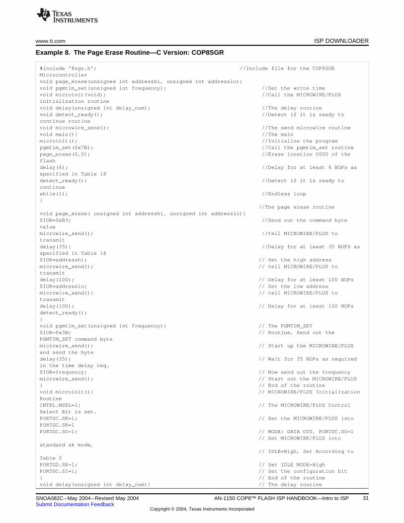
www.ti.com ISP DOWNLOADER
Example 8. The Page Erase Routine—C Version: COP8SGR
#include "8sgr.h"; //Include file for the COP8SGRMicrocontrollervoid page_erase(unsigned int addresshi, unsigned int addresslo);void pgmtim_set(unsigned int frequency); //Set the write timevoid microinit(void); //Call the MICROWIRE/PLUSinitialization routinevoid delay(unsigned int delay_num); //The delay routinevoid detect_ready(); //Detect if it is ready tocontinue routinevoid microwire_send(); //The send microwire routinevoid main() //The mainmicroinit(); //Initialize the programpgmtim_set(0x7B); //Call the pgmtim_set routinepage_erase(0,0); //Erase location 0000 of theflashdelay(6); //Delay for at least 6 NOPs asspecified in Table 18detect_ready(); //Detect if it is ready tocontinuewhile(1); //Endless loop
//The page erase routinevoid page_erase( unsigned int addresshi, unsigned int addresslo)SIOR=0xB3; //Send out the command bytevaluemicrowire_send(); //tell MICROWIRE/PLUS totransmitdelay(35); //Delay for at least 35 NOPS asspecified in Table 18SIOR=addresshi; // Set the high addressmicrowire_send(); // tell MICROWIRE/PLUS totransmitdelay(100); // Delay for at least 100 NOPsSIOR=addresslo; // Set the low addressmicrowire_send(); // tell MICROWIRE/PLUS totransmitdelay(100); // Delay for at least 100 NOPsdetect_ready();void pgmtim_set(unsigned int frequency) // The PGMTIM_SETSIOR=0x3B; // Routine, Send out thePGMTIM_SET command bytemicrowire_send(); // Start up the MICROWIRE/PLUSand send the bytedelay(35); // Wait for 35 NOPs as requiredin the time delay req.SIOR=frequency; // Now send out the frequencymicrowire_send(); // Start out the MICROWIRE/PLUS // End of the routinevoid microinit() // MICROWIRE/PLUS InitializationRoutineCNTRL.MSEL=1; // The MICROWIRE/PLUS ControlSelect Bit is set.PORTGC.SK=1; // Set the MICROWIRE/PLUS intoPORTGC.SK=1PORTGC.SO=1; // MODE: DATA OUT, PORTGC.SO=1
// Set MICROWIRE/PLUS intostandard sk mode,
// IDLE=High, Set According toTable 2PORTGD.SK=1; // Set IDLE MODE=HighPORTGC.SI=1; // Set the configuration bit // End of the routinevoid delay(unsigned int delay_num) // The delay routine
31SNOA082C–May 2004–Revised May 2004 AN-1150 COP8™ FLASH ISP HANDBOOK—Intro to ISPSubmit Documentation Feedback
Copyright © 2004, Texas Instruments Incorporated

ISP DOWNLOADER www.ti.com
Example 8. The Page Erase Routine—C Version: COP8SGR (continued)
unsigned int i; // temp variablefor (i=0;i<delay_num; i++) // The loop controlNOP; // Wait on NOP // End of the delay routinevoid detect_ready() // Detect if the host is readyto send routinePORTGC.SK=0; // Set the PORTG.SK into inputmodePORTGD.SK=0;while(PORTGP.SK==0) // While the CLOCK line is stilllowNOP; // Stay HerePORTGC.SK=1; //Other wise resetPORTGD.SK=1; //And Exit Routine //End of detect_ready()void microwire_send(void) // The routine that starts themicrowireCNTRL.MSEL=1; // Set the MICROWIRE/PLUSControl BitPSW.BUSY=1; // Set the PSW busy bitwhile(PSW.BUSY); // Wait until the bit has cleared // end of the routine
4.1.4 MASS_ERASE—Bulk Erase the Flash Memory
Figure 29 shows the flow for the MASS_ERASE routine. Example 9 and Example 10 shows the assemblyand C code versions of the MASS_ERASE routine.
Figure 29. Flow for the Mass Erase Function
Example 9. The Mass Erase Routine—Assembly Version: COP8SGR
; Mass Erase The FLASH.INCLD cop8sgr.INC ;INCLUDE FILE FOR THE COP8SGR.sect DATA,REG,ABS=0F0;DELAY_NUM .DSB 1 ;Allocate some memoryADDRESSHI .DSB 1 ;To Hold the Upper ByteADDRESSLO .DSB 1 ;To Hold the Lower Byte
32 AN-1150 COP8™ FLASH ISP HANDBOOK—Intro to ISP SNOA082C–May 2004–Revised May 2004Submit Documentation Feedback
Copyright © 2004, Texas Instruments Incorporated

www.ti.com ISP DOWNLOADER
Example 9. The Mass Erase Routine—Assembly Version: COP8SGR (continued)
.SECT CODE,ROM,ABS=0 ;Beginning of the codeMAIN: ;Beginning of the mainjsr MICROINIT ;Call the initialization routinejsr PGMTIM_SET ;Set the PGMTIM_SET routineld ADDRESSHI,#000 ;Addresshi=0ld ADDRESSLO,#000 ;Addresslo=0jsr Mass_ERASE ;Call the Mass Erase routineld A,#006 ;Create a delay of at least 6 NOPSjsr DELAY ;Jump to the delay routinejp MAIN ;Return to the main functionMASS_ERASE: ;The erase functionld SIOR,#0BF ;The command byte for page erasejsr MICROWIRE_SEND ;Start the MICROWIRE/PLUS upld A,#023 ;Wait at least 35 cyclesjsr DELAY ;Call the delay routineld A,#055 ;Load the confirmation code into the SIORregisterx A,SIOR ;Do the swap herejsr MICROWIRE_SEND ;Start the MICROWIRE/PLUS upld A,#064 ;Create a delay of at least 100 NOPSjsr DELAY ;Jump to the delay routinejsr DETECT_READY ;Detect if its ready to continue
;Variable Host Delay implementationret ;Return from the callDETECT_READY: ;Variable Host Delay routinerbit SK,PORTGC ;Set portg.sk into read only moderbit SK,PORTGD ;VARIABLE_DELAY: ;The holding is hereifbit SK,PORTGP ;If high then return and proceed to nextjp NEXT ;instructionjp VARIABLE_DELAY ;Otherwise stay hereNEXT: ; Continue on to the next instructionsbit SK,PORTGC ; Reset to normal mode when donesbit SK,PORTGD ;ret ; Return to function callMICROWIRE_SEND: ; The MICROWIRE/PLUS send routinesbit BUSY,PSW ; SET THE PSW.BUSY BIT TO TURN ONwait_uwire: ; THE MICROWIRE WAIT ROUTINEifbit BUSY,PSW ; IF THE BIT IS ON THEN WAITjp wait_uwire ; Otherwise stay in the loopret ; End of MICROWIRE/PLUS_SENDDELAY: ;THE DELAY ROUTINE
; ASSUME THE AMOUNT OF NOPS IS STORED IN; THE ACCUMULATOR A
x A,DELAY_NUM ; SET THE DELAY_NUM VARIABLELOOP_POINT: ; POINT WHERE THE LOOP ACTUALLY OCCURSNOP ; THE ACTUAL NOPSdrsz DELAY_NUM ; DECREMENT DELAY_NUM, SKIP NEXT INSTR. IFjp LOOP_POINT ; ZEROret ; End of DELAYPGMTIM_SET: ; THE SET WRITE TIMING ROUTINEld SIOR,#03B ; PGMTIM_SET COMMAND Bytejsr MICROWIRE_SEND ; Send the command byte outld A,#023 ; The amount of delay cycles required, For moreinformation
; see 2-11 regarding required time delay cyclesjsr DELAY ; The delay routineld SIOR,# 07B ; Send the Write Time -Assume a 10MHz CKI CBR CKI
; frequency, See Table 2-13 for other valuesjsr MICROWIRE_SEND ; Send the value out to the COP8CBRret ; End of PGMTIM_SET ProgramMICROINIT:sbit MSEL,CNTRL ; CNTRL.MSEL= 1, SET MICROWIRE INTO
33SNOA082C–May 2004–Revised May 2004 AN-1150 COP8™ FLASH ISP HANDBOOK—Intro to ISPSubmit Documentation Feedback
Copyright © 2004, Texas Instruments Incorporated

ISP DOWNLOADER www.ti.com
Example 9. The Mass Erase Routine—Assembly Version: COP8SGR (continued)
sbit SK,PORTGC ; PORTGC.SK = 1, MODE, DATA OUT,sbit SO,PORTGC ; PORTGC.SO = 1, DATA INrbit SO,PORTGD ; PORTGD.SO = 0 to let the firmware know that
; you want to go into ISP Mode; Set MICROWIRE/PLUS into standard sk mode,; IDLE = High, SET ACCORDING TO Table 20
sbit SK,PORTGD ; PORTGD.SK=1sbit SI,PORTGC ; PORTGC.SI = 1ret ; RETURN FROM THE CALL.END MAIN ; END OF PROGRAM
Example 10. The Mass Erase Routine—C Version: COP8SGR
#include "8sgr.h"; // Include file for the COP8SGR Microcontrollervoid mass_erase();void pgmtim_set(unsigned int frequency); // Set the write timevoid microinit(void); // Call the MICROWIRE/PLUS initialization routinevoid delay(unsigned int delay_num); // The delay routinevoid detect_ready(); // Detect if it is ready to continue routinevoid microwire_send(); // Send the data out that is in the SIOR buffervoid main() // The mainmicroinit(); // Initialize the programpgmtim_set(0x7B); // Call the pgmtim_set routinemass_erase(); // Mass erase the flashdelay(6); //Delay for at least 6 NOPs as specified in Table18detect_ready(); // Detect if it is ready to continuewhile(1); // Endless loop
// The mass erase routinevoid mass_erase( )SIOR=0xBF; // Send out the command byte valuemicrowire_send(); // tell MICROWIRE/PLUS to transmitdelay(35); // Delay for at least 35 NOPS as specified in theTable 18SIOR=0x55; // Set the confirmation codemicrowire_send(); // tell MICROWIRE/PLUS to transmitdelay(100); // Delay for at least 100 NOPsdetect_ready();void pgmtim_set(unsigned int frequency) // The PGMTIM_SETSIOR=0x3B; // Routine, Send out the PGMTIM_SET command bytemicrowire_send(); // Start up the MICROWIRE/PLUS and send the bytedelay(35); // Wait for 35 NOPs as required in the time delayreq.SIOR=frequency; // Now send out the frequencymicrowire_send(); // Start out the MICROWIRE/PLUS // End of the routinevoid microinit() // MICROWIRE/PLUS Initialization RoutineCNTRL.MSEL=1; // The MICROWIRE/PLUS Control Select Bit is set.PORTGC.SK=1; // Set the MICROWIRE/PLUS into PORTGC.SK=1PORTGC.SO=1; // MODE: DATA OUT, PORTGC.SO=1
// Set MICROWIRE/PLUS into standard sk mode,IDLE=High,
// Set According to Table 2PORTGD.SK=1; // Set IDLE MODE=HighPORTGC.SI=1; // Set the configuration bit // End of the routinevoid delay(unsigned int delay_num) // The delay routineunsigned int i; // temp variablefor (i=0; i<delay_num; i++) // The loop control
34 AN-1150 COP8™ FLASH ISP HANDBOOK—Intro to ISP SNOA082C–May 2004–Revised May 2004Submit Documentation Feedback
Copyright © 2004, Texas Instruments Incorporated

www.ti.com ISP DOWNLOADER
Example 10. The Mass Erase Routine—C Version: COP8SGR (continued)
NOP; // Wait on NOP // End of the delay routinevoid detect_ready() // Detect if the host is ready to send routinePORTGC.SK=0; // Set the PORTG.SK into input modePORTGD.SK=0;while(PORTGP.SK==0) // While the CLOCK line is still lowNOP; // Stay HerePORTGC.SK=1; // Otherwise resetPORTGD.SK=1; // And Exit Routine // End of detect_ready()void microwire_send(void) // The routine that starts the microwireCNTRL.MSEL=1; // Set the MICROWIRE/PLUS Control BitPSW.BUSY=1; // Set the PSW busy bitwhile(PSW.BUSY); // Wait until the bit has cleared // end of the routine
4.1.5 READ_BYTE—Read a Byte from the Flash Memory Array
Figure 30 shows the flow for the READ_BYTE routine. Example 11 and Example 12 shows the assemblyand C code versions for the routine.
Figure 30. Flow for the Read Byte Routine
Example 11. Read A Byte Of Flash—Assembly Version: COP8SGR
; The following routine will read a byte from the flash memory array.INCLD cop8sgr.INC ;INCLUDE FILE FOR THE COP8SGR.sect DATA,REG,ABS=0F0 ;Set the beginning of the RAM locationDELAY_NUM .DSB 1 ;To be starting at 0F0ADDRESSHI .DSB 1 ;The high address byteADDRESSLO .DSB 1 ;The low address byte
35SNOA082C–May 2004–Revised May 2004 AN-1150 COP8™ FLASH ISP HANDBOOK—Intro to ISPSubmit Documentation Feedback
Copyright © 2004, Texas Instruments Incorporated

ISP DOWNLOADER www.ti.com
Example 11. Read A Byte Of Flash—Assembly Version: COP8SGR (continued)
DATA_READ .DSB 1 ;The variable to store the returned data.SECT CODE,ROM,ABS=0 ;Beginning of the codeMAIN: ;The Mainjsr MICROINIT ;Call the MICROWIRE/PLUS initialization routineld ADDRESSHI,#000 ;Addresshi = 0 of flashld ADDRESSLO,#000 ;Addresslo = 0 of flashjsr READ_BYTE ;Call the read byte routineld A,#006 ;Delay for 6 cyclesjsr DELAY ;Call the delay routineld A,SIOR ;Copy the buffer into the accumulatorx A,DATA_READ ;Save into the RAM location nowjp MAIN ;Return to the mainREAD_BYTE: ;The read byte routineld SIOR,#01D ;The command byte for read bytejsr MICROWIRE_SEND ;Call the MICROWIRE/PLUS send routineld A,#023 ;Delay for 35 cyclesjsr DELAY ;Call the delay functionld A,ADDRESSHI ;Set the actual high byte if the flash addressx A,SIOR ;Swap it with the MICROWIRE/PLUS buffer and send it outjsr MICROWIRE_SEND ;Call the MICROWIRE/PLUS send routineld A,#064 ;Delay for 100 NOPsjsr DELAY ;Call the delay routineld A, ADDRESSLO ;Set the actual low byte of the flash addressx A,SIOR ;Swap it with SIORjsr MICROWIRE_SEND ;Call the MICROWIRE/PLUS send routineld A,#064 ;Wait for 100 Nopsjsr MICROWIRE_SEND ;One last time to get the data
;Data should be in the SIOR register nowjsr DELAY ;Call the delay routinejsr MICROWIRE_SEND ;ONE LAST CALL FOR THE DATA
;DATA SHOULD BE IN THE SIOR NOWret ;MICROWIRE_SEND: ; MICROWIRE/PLUS Routinesbit BUSY,PSW ; SET THE PSW.BUSY BIT TO TURN ONwait_uwire: ; THE MICROWIRE WAIT ROUTINEifbit BUSY,PSW ; IF THE BIT IS ON THEN WAITjp wait_uwire ; Otherwise stay in the loopret ; End of MICROWIRE/PLUS_SENDDELAY: ; THE DELAY ROUTINE
; ASSUME THE AMOUNT OF NOPS IS STORED IN; THE ACCUMULATOR A
x A,DELAY_NUM ; SET THE DELAY_NUM VARIABLELOOP_POINT: ; POINT WHERE THE LOOP ACTUALLY OCCURSNOP ; THE ACTUAL NOPSdrsz DELAY_NUM ; DECREMENT DELAY_NUM, SKIP NEXT INSTR. IFjp LOOP_POINT ; ZEROret ; End of DELAYMICROINIT:sbit MSEL,CNTRL ; CNTRL.MSEL= 1, SET MICROWIRE INTOsbit SK,PORTGC ; PORTGC.SK = 1, MODE, DATA OUT,sbit SO,PORTGC ; PORTGC.SO = 1, DATA INrbit SO,PORTGD ; PORTGD.SO = 0 to let the firmware know that
; you want to go into ISP Mode; Set MICROWIRE/PLUS into standard sk mode,; IDLE = High, SET ACCORDING TO Table 20
sbit SK,PORTGD ; PORTGD.SK=1sbit SI,PORTGC ; PORTGC.SI = 1ret ; RETURN FROM THE CALL.END MAIN ; END OF PROGRAM
36 AN-1150 COP8™ FLASH ISP HANDBOOK—Intro to ISP SNOA082C–May 2004–Revised May 2004Submit Documentation Feedback
Copyright © 2004, Texas Instruments Incorporated

www.ti.com ISP DOWNLOADER
Example 12. Read A Byte of Flash—C Version: COP8SGR
#include "8sgr.h"; //Include file for the COP8SGRMicrocontrollerunsigned int read_byte(unsigned int addresshi, unsigned int addresslo); //The readbyte functionvoid microinit(void); //The MICROWIRE/PLUSinitialization routinevoid delay(unsigned int delay_num); //The delay routinevoid microwire_send(); //The microwire sendroutinevoid main() //The main routineunsigned int data_read; //The buffer that would holdthe result datamicroinit(); //Initialize the data vectordata_read=read_byte(0,1); //Read at location 1 of theflashwhile(1); //Endless loop
//The read_byte routine, itwill return the data byte readunsigned int read_byte( unsigned int addresshi, unsigned in addresslo)SIOR=0x1D; //The read_byte command bytemicrowire_send(); //Send it out to theMICROWIRE/PLUSdelay(35); //Wait for 35 NOPs as statedin Table 18SIOR=addresshi; //Set up the high addressmicrowire_send(); //Send it out on theMICROWIRE/PLUS linedelay(100); //Wait for 100 NopsSIOR=addresslo; //Set up the low addressmicrowire_send(); //Send it out on theMICROWIRE/PLUS linedelay(100); //Wait for 100 Nopsmicrowire_send(); //One last time for the datareturn SIOR; //Data should now be in theSIOR buffer //End of read_byte routinevoid microinit() // MICROWIRE/PLUSInitialization RoutineCNTRL.MSEL=1; // The MICROWIRE/PLUS ControlSelect Bit is set.PORTGC.SK=1; // Set the MICROWIRE/PLUS intoPORTGC.SK=1PORTGC.SO=1; // MODE: DATA OUT, PORTGC.SO=1PORTGD.SO=0; // To tell the firmware that youwant to go into
// ISP Mode// Set MICROWIRE/PLUS into standard
sk mode, IDLE=High,// Set According to Table 2
PORTGD.SK=1; // Set IDLE MODE=HighPORTGC.SI=1; // Set the configuration bit // End of microinit routinevoid delay(unsigned int delay_num) // The delay routineunsigned int i; // temp variablefor (i-0; i<delay_num;i++) // The loop controlNOP; // Wait on NOP // End of the delay routinevoid microwire_send(void) // The routine that starts themicrowireCNTRL.MSEL=1; // Set the MICROWIRE/PLUS ControlBitPSW.BUSY=1; // Set the PSW busy bitwhile(PSW.BUSY); // Wait until the bit has cleared
37SNOA082C–May 2004–Revised May 2004 AN-1150 COP8™ FLASH ISP HANDBOOK—Intro to ISPSubmit Documentation Feedback
Copyright © 2004, Texas Instruments Incorporated

ISP DOWNLOADER www.ti.com
Example 12. Read A Byte of Flash—C Version: COP8SGR (continued)
// end of the routine
4.1.6 WRITE_BYTE—Write a Byte to the Flash Memory Array
Figure 31 shows the flow for the WRITE_BYTE routine. Example 13 and Example 14 and shows theassembly and C code versions for the routine.
Figure 31. Flow for the Write Byte Function
Example 13. Write a Byte to the Flash—Assembly Version: COP8SGR
; WRITE A BYTE TO THE FLASH ROUTINE.INCLD cop8sgr.INC ;INCLUDE FILE FOR THE COP8SGR.sect DATA,REG,ABS=0F0 ;DECLARE SOME VARIABLEDELAY_NUM .DSB 1 ;The number of delaysADDRESSHI .DSB 1 ;The high address byteADDRESSLO .DSB 1 ;The low address byteWRITE_DATA .DSB 1 ;The variable where the data is to be read
; from.SECT CODE,ROM,ABS=0 ;Beginning of the programMAIN: ;The main routinejsr MICROINIT ;Initialize the MICROWIRE/PLUSjsr PGMTIM_SET ;Set the write timeld A,#006 ;Delay for 6 cyclesjsr DELAY ;Call the delay routineld ADDRESSHI,#000 ;Set the high address byteld ADDRESSLO,#001 ;Set the low address byteld WRITE_DATA,#005 ;Load a 5 where the write data variable isjsr WRITE_BYTE ;Call the write byte variablejp MAIN ;Jump to the main functionWRITE_BYTE: ;The write byte variableld SIOR,#071 ;The write byte command valuesjsr MICROWIRE_SEND ;Start-up the MICROWIRE/PLUS functionld A,#023 ;Delay for 35 Nopsjsr DELAY ;Call the delay functionld A,ADDRESSHI ;Set the high address byte
38 AN-1150 COP8™ FLASH ISP HANDBOOK—Intro to ISP SNOA082C–May 2004–Revised May 2004Submit Documentation Feedback
Copyright © 2004, Texas Instruments Incorporated

www.ti.com ISP DOWNLOADER
Example 13. Write a Byte to the Flash—Assembly Version: COP8SGR (continued)
x A,SIOR ;Then swap it with the SIOR registerjsr MICROWIRE_SEND ;Call the MICROWIRE/PLUS send routineld A,#064 ;Delay for 100 Nopsjsr DELAY ;Call the delay routineld A, ADDRESSLO ;Set the low address bytex A,SIOR ;Swap it with the SIOR registerjsr MICROWIRE_SEND ;Call the MICROWIRE/PLUS send routineld A,#014 ;Delay for 20 Nopsjsr DELAY ;Call the delay routineld A, WRITE_DATA ;Set the low address bytex A,SIOR ;Swap it with the SIOR registerjsr MICROWIRE_SEND ;Call the MICROWIRE/PLUS send routineld A,#014 ;Delay for 20 Nopsjsr DELAY ;Call the delay routineld A,WRITE_DATA ;Get the datax A,SIOR ;Get ready to send it outjsr MICROWIRE_SEND ;ONE LAST CALL FOR THE DATAld A,#00A ;Delay for 10 Nopsjsr DELAY ;Call the delay routinejsr DETECT_READY ;Call the routine to detect if it is readyret ;Return to the function callPGMTIM_SET: ;THE SET WRITE TIMING ROUTINEld SIOR,#03B ;PGMTIM_SET COMMAND Bytejsr MICROWIRE_SEND ;Send the command byte outld A,#023 ; The amount of delay cycles required, For more informa-
; tion see Table 18 regarding required time delay cyclesjsr DELAY ; The delay routineld SIOR,# 07B ; Send the Write Time - Assume a 10MHz CKI CBR; CKI frequencyld A,#064 ; The amount of delay cycles required, For more informa-
; tion see Table 18 regarding required time delay cyclesjsr DELAY ; The delay routinejsr MICROWIRE_SEND ; Send the value out to the COP8CBRret ; End of PGMTIM_SET routineDETECT_READY: ; Variable Host Delay routinerbit SK,PORTGC ; Set portg.sk into read only moderbit SK,PORTGD ;VARIABLE_DELAY: ; The holding is hereifbit SK,PORTGP ; If high then return and proceed to nextjp NEXT ; instructionjp VARIABLE_DELAY ; Otherwise stay hereNEXT: ; Continue on to the next instructionsbit SK,PORTGC ; Reset to normal mode when donesbit SK,PORTGD ;ret ;Return to function callDELAY: ; THE DELAY ROUTINE
; ASSUME THE AMOUNT OF NOPS IS STORED IN; THE ACCUMULATOR A
x A,DELAY_NUM ; SET THE DELAY_NUM VARIABLELOOP_POINT: ; P01NT WHERE THE LOOP ACTUALLY OCCURSNOP ; THE ACTUAL NOPSdrsz DELAY_NUM ; DECREMENT DELAY_NUM, SKIP NEXT INSTR. IFjp LOOP_POINT ; ZEROret ; End of DELAYMICROINIT:sbit MSEL,CNTRL ; CNTRL.MSEL= 1, SET MICROWIRE INTOsbit SK,PORTGC ; PORTGC.SK = 1, MODE, DATA OUT,sbit SO,PORTGC ; PORTGC.SO = 1, DATA INrbit SO,PORTGD ; PORTGD.SO = 0 to let the firmware know that
; you want to go into ISP Mode; Set MICROWIRE/PLUS into standard sk mode,
; IDLE = High, SET ACCORDING TO Table 20sbit SK,PORTGD ; PORTGD.SK=1sbit SI,PORTGC ; PORTGC.SI = 1
39SNOA082C–May 2004–Revised May 2004 AN-1150 COP8™ FLASH ISP HANDBOOK—Intro to ISPSubmit Documentation Feedback
Copyright © 2004, Texas Instruments Incorporated

ISP DOWNLOADER www.ti.com
Example 13. Write a Byte to the Flash—Assembly Version: COP8SGR (continued)
ret ; RETURN FROM THE CALLMICROWIRE_SEND: ; MICROWIRE/PLUS Routinesbit BUSY,PSW ; SET THE PSW.BUSY BIT TO TURN ONwait_uwire: ; THE MICROWIRE WAIT ROUTINEifbit BUSY,PSW ; IF THE BIT IS ON THEN WAITjp wait_uwire ; Otherwise stay in the loopret ; End of MICROWIRE/PLUS_SEND.END MAIN ; End of the Program
Example 14. Write a Byte to the Flash—C Version: COP8SGR
#include "8sgr.h"; // Include file for the COP8SGR Microcontrollervoid write_byte(unsigned int addresshi, unsigned int addresslo, usigned int write_data);
// The write byte routinevoid microinit(void); // Initialize the MICROWIRE/PLUS initializationvoid delay(unsigned int delay_num); // Delay routinevoid detect_ready(); // Detect when CBR is readyvoid microwire_send(); // The microwire send routinevoid main() // The main routinemicroinit(); // The main initialization routinepgmtim_set(0x7B); // Call the pgmtim_set routinewrite_byte(0,1,5); // Write a byte at location 1 of flash with a 5detect_ready();while(1); // Endless loopvoid pgmtim_set(unsigned int frequency) // The PGMTIM_SETSIOR=0x3B; // Routine, Send out the PGMTIM_SET command bytemicrowire_send(); // Start up the MICROWIRE/PLUS and send the bytedelay(35); // Wait for 35 NOPs as required in the time delay req.SIOR=frequency; // Now send out the frequencymicrowire_send(); // Start out the MICROWIRE/PLUSdelay(100); // Wait for at least 100 NOPs // End of the routinevoid write_byte( unsigned int addresshi, unsigned in addresslo, unsigned int write_data)
// The actual function callSIOR=0x1D; // The command byte valuemicrowire_send(); // Send it out to the CBRdelay(35); // Delay for 35 NopsSIOR=addresshi; // Send out the high address bytemicrowire_send(); // Tell MICROWIRE/PLUS to send itdelay(100); // Delay for 100 NopsSIOR=addresslo; // Send out the low address bytemicrowire_send(); // Tell MICROWIRE/PLUS to send itdelay(100); // Delay for 100 Nopsmicrowire_send(); // Now send the actual data to the microcontrollerdelay(10); // Wait till the end of 10 cyclesdetect_ready(); // Detect if the CBR is ready for additional data // end of the write_byte routinevoid microinit() // MICROWIRE/PLUS Initialization RoutineCNTRL.MSEL=1; // The MICROWIRE/PLUS Control Select Bit is setPORTGC.SK=1; // Set the MICROWIRE/PLUS into PORTGC.SK=1PORTGC.SO=1; // MODE: DATA OUT, PORTGC.SO=1PORTGD.SO=0; // To tell the firmware that you want to go into
// ISP Mode// Set MICROWIRE/PLUS into standard sk mode, IDLE=High,// Set According to Table 2
PORTGD.SK=1; // Set IDLE MODE=HighPORTGC.SI=1; // Set the configuration bit // End of microinit routinevoid detect_ready() //Detect if the host is ready to send routinePORTGC.SK=0; //Set the PORTG.SK into input mode
40 AN-1150 COP8™ FLASH ISP HANDBOOK—Intro to ISP SNOA082C–May 2004–Revised May 2004Submit Documentation Feedback
Copyright © 2004, Texas Instruments Incorporated

www.ti.com ISP DOWNLOADER
Example 14. Write a Byte to the Flash—C Version: COP8SGR (continued)
PORTGD.SK=0;while(PORTGP.SK==0) //While the CLOCK line is still lowNOP; //Stay HerePORTGC.SK=1; //Otherwise resetPORTGD.SK=1; //And Exit Routine //End of detect_ready()void delay(unsigned int delay_num) // The delay routineunsigned int i; // temp variablefor (i=0;i<delay_num;i++) // The loop controlNOP; // Wait on NOP //End of delay routinevoid detect_ready() // Detect if the host is ready to send routinePORTGC.SK=0; //Set the PORTG.SK into input modePORTGD.SK=0;while(PORTGP.SK==0) //While the CLOCK line is still lowNOP; //Stay HerePORTGC.SK=1; //Otherwise resetPORTGD.SK=1; /And Exit Routine //End of the detect ready eventvoid microwire_send(void) // The routine that starts the microwireCNTRL.MSEL=1; // Set the MICROWIRE/PLUS Control BitPSW.BUSY=1; // Set the PSW busy bitwhile(PSW.BUSY); // Wait until the bit has cleared // end of the routine
4.1.7 BLOCK WRITE—Write a Block of Data to the Flash Memory Array
Figure 32 shows the flow for the BLOCK WRITE routine. Example 15 and Example 16 shows theassembly and C code versions for the routine.
Figure 32. Flow for the Block Write Function
Example 15. The Block Write Sample Code—Assembly Version: COP8SGR
; WRITE A BLOCK OF DATA TO THE FLASH MEMORY.INCLD cop8sgr.INC ;INCLUDE FILE FOR THE COP8SGR.sect DATA,REG,ABS=0F0 ;Declare some variables
41SNOA082C–May 2004–Revised May 2004 AN-1150 COP8™ FLASH ISP HANDBOOK—Intro to ISPSubmit Documentation Feedback
Copyright © 2004, Texas Instruments Incorporated

ISP DOWNLOADER www.ti.com
Example 15. The Block Write Sample Code—Assembly Version: COP8SGR (continued)
DELAY_NUM .DSB 1 ;For the delay routineADDRESSHI .DSB 1 ;To hold the high address byteADDRESSLO .DSB 1 ;To hold the low address byteBYTECOUNTLO .DSB 1 ;To hold the number of bytes to sendWRITE_DATA1 .DSB 1 ;To hold the sample data #1WRITE_DATA2 .DSB 1 ;To hold the sample data #2WRITE_DATA3 .DSB 1 ;To hold the sample data #3.SECT CODE,ROM,ABS=0 ;Beginning of the programMAIN: ;The main functionjsr PGMTIM_SET ;Set the write timeld A,#006 ;Delay for 6 Nops before jumpingjsr DELAY ;Call the delay routinejsr MICROINIT ;Initialize the MICROWIRE/PLUS routineld WRITE_DATA1,#001 ;Set the first variable WRITE_DATA1=1ld WRITE_DATA2,#002 ;Set the second var. WRITE_DATA2=2ld WRITE_DATA3,#003 ;Set the third var. WRITE_DATA3=3ld ADDRESSHI,#000 ;The high address byte is 0ld ADDRESSLO,#001 ;The low address byte is 1ld B,#WRITE_DATA1 ;Set the pointer to the WRITE_DATA1ld BYTECOUNTLO,#003 ;Set the number of bytes to read as 3jsr BLOCK_WRITE ;Call the block write routineld A,#006 ;Delay for 6 Nopsjsr DELAY ;Call the delay routinejp MAIN ;Return to the MAIN functionBLOCK_WRITE: ;The BLOCK_WRITE routine definitionld SIOR,#08F ;The BLOCK_WRITE command bytejsr MICROWIRE_SEND ;Startup MICROWIRE/PLUSld A,#023 ;Delay for 35 Nops as specified in Table 18jsr DELAY ;Call the delay routineld A,ADDRESSHI ;Load the high byte of the address to thex A,SIOR ;SIOR Bufferjsr MICROWIRE_SEND ;Send it out to the COP8CBRld A,#064 ;Delay for 100 Nopsjsr DELAY ;Call the delay functionld A, ADDRESSLO ;Load the low byte of the address to thex A,SIOR ;SIOR Bufferjsr MICROWIRE_SEND ;Send it out to the COP8CBRld A,#064 ;Delay for 100 Nopsjsr DELAY ;Call the delay functionld A,BYTECOUNTLO ;Load the value of bytecountlo into the
; accumulatorx A,SIOR ;Swap it with the SIOR bufferjsr MICROWIRE_SEND ;Call MICROWIRE/PLUS to send it outld A,#064 ;Setup a delay for 100 Nopsjsr DELAY ;Call the delay functionREAD_PT: ;The point where the read loops aroundld A,[B+] ;Load the value where the B pointer is pointing atx A,SIOR ;It assume the user has already setup the B pointerjsr MICROWIRE_SEND ;Call the MICROWIRE/PLUS to send it outld A,#064 ;Swap it with the SIOR buffer and delays it for 100 Nopsjsr DELAY ;Call the delay routinedrsz BYTECOUNTLO ;Decrement bytecount and jump next if zerojp READ_PT ;Go back to the read pointjsr DETECT_READY ;Detect if it is ready to sendret ;End of Block Write RoutineDETECT_READY: ;Variable Host Delay routinerbit SK,PORTGC ;Set portg.sk into read only moderbit SK,PORTGD ;VARIABLE_DELAY: ;The holding is hereifbit SK,PORTGP ;If high then return and proceed to nextjp NEXT ;instructionjp VARIABLE_DELAY ;Otherwise stay hereNEXT: ;Continue the next instructionsbit SK,PORTGC ;Reset to normal mode when done
42 AN-1150 COP8™ FLASH ISP HANDBOOK—Intro to ISP SNOA082C–May 2004–Revised May 2004Submit Documentation Feedback
Copyright © 2004, Texas Instruments Incorporated

www.ti.com ISP DOWNLOADER
Example 15. The Block Write Sample Code—Assembly Version: COP8SGR (continued)
sbit SK,PORTGD ;ret ;Return to function callDELAY: ;THE DELAY ROUTINE
; ASSUME THE AMOUNT OF NOPS IS STORED IN; THE ACCUMULATOR A
x A,DELAY_NUM ;SET THE DELAY_NUM VARIABLELOOP_POINT: ;P01NT WHERE THE LOOP ACTUALLY OCCURSNOP ;THE ACTUAL NOPSdrsz DELAY_NUM ;DECREMENT DELAY_NUM, SKIP NEXT INSTR. IFjp LOOP_POINT ;ZEROret ;End of DELAYMICROINIT:sbit MSEL,CNTRL ; CNTRL.MSEL= 1, SET MICROWIRE INTOsbit SK,PORTGC ; PORTGC.SK = 1, MODE, DATA OUT,sbit SO,PORTGC ; PORTGC.SO = 1, DATA INrbit SO,PORTGD ; PORTGD.SO = 0 to let the firmware know that
; you want to go into ISP Mode; Set MICROWIRE/PLUS into standard sk mode,; IDLE = High, SET ACCORDING TO Table 20
sbit SK,PORTGD ; PORTGD.SK=1sbit SI,PORTGC ; PORTGC.SI = 1ret ; RETURN FROM THE CALLPGMTIM_SET: ; THE SET WRITE TIMING ROUTINEld SIOR,#03B ; PGMTIM_SET COMMAND Bytejsr MICROWIRE_SEND ; Send the command byte outld A,#023 ; The amount of delay cycles required, For more informa-
; tion see Table 18 regarding required time delay cyclesjsr DELAY ; The delay routineld SIOR,# 07B ; Send the Write Time - Assume a 10MHz CKI CBR CKI frequencyjsr MICROWIRE_SEND ; Send the value out to the COP8CBRld A,#064 ; The amount of delay cycles required, For more informa-
; tion see Table 18 regarding required time delay cyclesjsr DELAY ; The delay routineret ; End of PGMTIM_SETMICROWIRE_SEND: ; MICROWIRE/PLUS Routinesbit BUSY,PSW ; SET THE PSW.BUSY BIT TO TURN ONwait_uwire: ; THE MICROWIRE WAIT ROUTINEifbit BUSY,PSW ; IF THE BIT IS ON THEN WAITjp wait_uwire ; Otherwise Wait until clearedret ; End of MICROWIRE/PLUS_SEND.END MAIN ; END OF PROGRAM
Example 16. The Block Write Sample Code–C Version: COP8SGR
#include "8sgr.h"; // Include file for the COP8SGR Microcontroller// The write byte routine
void block_write(unsigned int addresshi, unsigned int addresslo, unsigned intbytecountlo); void microinit(void); // Initialize the// MICROWIRE/PLUS initalizationvoid delay(unsigned int delay_num); // Delay it for 6 Nopsvoid detect_ready(); // Detect when CBR is readyvoid microwire_send(); // The microwire send routineunsigned int write_data[3]; // Declare three data points for data storagevoid main() //The main routinemicroinit(); //The main initialization routinepgmtim_set(0x7B); //Call the pgmtim_set routinewrite_data[1]=1; //Storage location 1 for the block write routinewrite_data[2]=2; //Storage location 2 for the block write routinewrite_data[3]=3; //Storage location 3 for the block write routineblock_write(0,1,3); //Write a block of data beginning at flash(001) and//bytecountlo=3, the assumed array is global with the name
43SNOA082C–May 2004–Revised May 2004 AN-1150 COP8™ FLASH ISP HANDBOOK—Intro to ISPSubmit Documentation Feedback
Copyright © 2004, Texas Instruments Incorporated

ISP DOWNLOADER www.ti.com
Example 16. The Block Write Sample Code–C Version: COP8SGR (continued)
write_data[]while(1); //Endless loopvoid block_write( unsigned int addresshi, unsigned int addresslo, unsignedint bytecountlo) //The actual function callunsigned int i; //A counter variableSIOR=0x8F; //The command byte valuemicrowire_send(); //Send it out to the CBRdelay(35); //Delay for 35 NopsSIOR=addresshi; //Send out the high address bytemicrowire_send(); //Tell MICROWIRE/PLUS to send itdelay(100); //Delay for 100 NopsSIOR=addresslo; //Send out the low address bytemicrowire_send(); //Tell MICROWIRE/PLUS to send itdelay(100); //Delay for 100 Nopsmicrowire_send(); //Now send the actual data to the microcontrollerSIOR=bytecountlo; //Send out the low address bytemicrowire_send(); //Tell MICROWIRE/PLUS to send itdelay(100); //Delay for 100 Nopsfor (i=0; i<bytecountlo;i++) //Send the data out until it reachesbytecountloSIOR=write_data[i]; //Send out the low address bytemicrowire_send(); //Tell MICROWIRE/PLUS to send itdelay(100); //Delay for 100 Nopsdetect_ready(); //Detect if the CBR is ready for additional data //end of the block write routinevoid microinit() // MICROWIRE/PLUS Initialization RoutineCNTRL.MSEL=1; // The MICROWIRE/PLUS Control Select Bit is set.PORTGC.SK=1; // Set the MICROWIRE/PLUS into PORTGC.SK=1PORTGC.SO=1; // MODE: DATA OUT, PORTGC.SO=1PORTGD.SO=0; // To tell the firmware that you want to go into
// ISP Mode// Set MICROWIRE/PLUS into standard sk mode, IDLE=High,// Set According to Table 2
PORTGD.SK=1; // Set IDLE MODE=HighPORTGC.SI=1; // Set the configuration bit // End of microinit routinevoid detect_ready() // Detect if the host is ready to continuePORTGC.SK=0; // Set the PORTG.SK into input modePORTGD.SK=0;while(PORTGP.SK==0) // While the CLOCK line is still lowNOP; // Stay HerePORTGC.SK=1; // Otherwise resetPORTGD.SK=1; // And Exit Routine // End of detect_ready()void pgmtim_set(unsigned int frequency) // The PGMTIM_SETSIOR=0x3B; // Routine, Send out the PGMTIM_SET command bytemicrowire_send(); // Start up the MICROWIRE/PLUS and send the bytedelay(35); // Wait for 35 NOPs as required in the time delay req.SIOR=frequency; // Now send out the frequencymicrowire_send(); // Start out the MICROWIRE/PLUSdelay(100); // End of the routinevoid microwire_send(void) // The routine that starts the microwireCNTRL.MSEL=1; // Set the MICROWIRE/PLUS Control BitPSW.BUSY=1; // Set the PSW busy bitwhile(PSW.BUSY); // Wait until the bit has cleared // end of the routine
44 AN-1150 COP8™ FLASH ISP HANDBOOK—Intro to ISP SNOA082C–May 2004–Revised May 2004Submit Documentation Feedback
Copyright © 2004, Texas Instruments Incorporated

www.ti.com ISP DOWNLOADER
4.1.8 BLOCK_READ_Read a Block from the Flash Memory Array
Figure 33 shows the flow for the BLOCK READ routine. Example 17 and Example 18 shows the assemblyand C code versions for the routine.
Figure 33. Flow for the BLOCK_READ Function
Example 17. The MICROWIRE/PLUS BLOCK_READ Routine—Assembly Routine: COP8SGR
;READ A BLOCK OF DATA FROM THE FLASH MEMORY.INCLD cop8sgr.INC ;INCLUDE FILE FOR THE COP8SGR.sect DATA,REG,ABS=0F0 ;Declare some variablesDELAY_NUM .DSB 1 ;For the delay routineADDRESSHI .DSB 1 ;To hold the high address byteADDRESSLO .DSB 1 ;To hold the low address byteBYTECOUNTLO .DSB 1 ;To hold the lower num of bytes to rec.BYTECOUNTHI .DSB 1 ;To hold the upper num of bytes to rec.READ_DATA1 .DSB 1 ;To hold the sample data #1READ_DATA2 .DSB 1 ;To hold the sample data #2READ_DATA3 .DSB 1 ;To hold the sample data #3.SECT CODE,ROM,ABS=0 ;Beginning of the programMAIN: ;The main functionjsr MICROINIT ;Initialize the MICROWIRE/PLUS routineld ADDRESSHI,#000 ;The high address byte is 0ld ADDRESSLO,#001 ;The low address byte is 1ld B,#READ_DATA1 ;Set the pointer to the READ_DATA1ld BYTECOUNTLO,#003 ;Set the lower num of bytes to read as 3ld BYTECOUNTHI,#000 ;Set the up num of bytes to readjsr BLOCK_WRITE ;Call the block write routineld A,#006 ;Delay for 6 Nopsjsr DELAY ;Call the delay routinejp MAIN ;Return to the MAIN functionBLOCK_READ: ;The BLOCK_WRITE routine definitionld SIOR,#0A3 ;The BLOCK_WRITE command bytejsr MICROWIRE_SEND ;Start-up the MICROWIRE/PLUS
45SNOA082C–May 2004–Revised May 2004 AN-1150 COP8™ FLASH ISP HANDBOOK—Intro to ISPSubmit Documentation Feedback
Copyright © 2004, Texas Instruments Incorporated

ISP DOWNLOADER www.ti.com
Example 17. The MICROWIRE/PLUS BLOCK_READ Routine—Assembly Routine: COP8SGR (continued)
ld A,#023 ;Delay for 35 Nops as specified in Table 18jsr DELAY ;Call the delay routineld A,ADDRESSHI ;Load the high byte of the address to thex A,SIOR ;SIOR Bufferjsr MICROWIRE_SEND ;Send it out to the COP8CBRld A,#064 ;Delay for 100 Nopsjsr DELAY ;Call the delay functionld A, ADDRESSLO ;Load the low byte of the address to thex A,SIOR ;SIOR Bufferjsr MICROWIRE_SEND ;Send it out to the COP8CBRld A,#064 ;Delay for 100 Nopsjsr DELAY ;Call the delay functionld A,BYTECOUNTHI ;Load the value of bytecountlo into the
;accumulatorx A,SIOR ;Swap it with the SIOR bufferjsr MICROWIRE_SEND ;Call MICROWIRE/PLUS to send it outld A,#064 ;Setup a delay for 100 Nopsjsr DELAY ;Call the delay functionld A,BYTECOUNTLO ;Load the value of bytecountlo into the accumulatorx A,SIOR ;Swap it with the SIOR bufferjsr MICROWIRE_SEND ;Call MICROWIRE/PLUS to send it outld A,#064 ;Setup a delay for 100 Nopsjsr DELAY ;Call the delay functionSAVE_PT: ;The point where the read loops aroundld A,#08C ;First wait until the delay is ready, 140 NOPsjsr DELAY ;by calling the delay routinejsr MICROWIRE_SEND ;Tell MICROWIRE/PLUS to send the data overld A,[B+] ;Load the value where the B pointer is pointing atx A,SIOR ;It assumes the user has already setup the B pointerdrsz BYTECOUNTLO ;Decrement bytecount and jump next if zerojp READ_PT ;Go back to the read pointjsr DETECT_READY ;Detect if it is ready to sendret ;Return to the callDETECT_READY: ;Variable Host Delay routinerbit SK,PORTGC ;Set portg.sk into read only moderbit SK,PORTGD ;VARIABLE_DELAY: ;The holding is hereifbit SK,PORTGP ;If high then return and proceed to nextjp NEXT ;instructionjp VARIABLE_DELAY ;Otherwise stay hereNEXT: ;Continue the next instructionsbit SK,PORTGC ;Reset to normal mode when donesbit SK,PORTGD ;ret ;Return to function callDELAY: ;THE DELAY ROUTINE
;ASSUME THE AMOUNT OF NOPS IS STORED IN;THE ACCUMULATOR A
x A,DELAY_NUM ;SET THE DELAY_NUM VARIABLELOOP_POINT: ;P01NT WHERE THE LOOP ACTUALLY OCCURSNOP ;THE ACTUAL NOPSdrsz DELAY_NUM ;DECREMENT DELAY_NUM, SKIP NEXT INSTR. IFjp LOOP_POINT ;ZEROret ;End of DELAYMICROINIT:sbit MSEL,CNTRL ;CNTRL.MSEL= 1, SET MICROWIRE INTOsbit SK,PORTGC ;PORTGC.SK = 1, MODE, DATA OUT,sbit SO,PORTGC ;PORTGC.SO = 1, DATA INrbit SO,PORTGD ;PORTGD.SO = 0 to let the firmware know that
;you want to go into ISP Mode;Set MICROWIRE/PLUS into standard sk mode,;IDLE = High, SET ACCORDING TO Table 20
sbit SK,PORTGD ;PORTGD.SK=1sbit SI,PORTGC ;PORTGC.SI = 1ret ;RETURN FROM THE CALL
46 AN-1150 COP8™ FLASH ISP HANDBOOK—Intro to ISP SNOA082C–May 2004–Revised May 2004Submit Documentation Feedback
Copyright © 2004, Texas Instruments Incorporated

www.ti.com ISP DOWNLOADER
Example 17. The MICROWIRE/PLUS BLOCK_READ Routine—Assembly Routine: COP8SGR (continued)
MICROWIRE_SEND: ;MICROWIRE/PLUS Send Routinesbit BUSY,PSW ;SET THE PSW.BUSY BIT TO TURN ONwait_uwire: ;THE MICROWIRE WAIT ROUTINEifbit BUSY,PSW ;IF THE BIT IS ON THEN WAITjp wait_uwire ;STAY MICROLOOP IF NOT DOTret ;End of MICROWIRE/PLUS_SEND.END MAIN ;END OF PROGRAM
Example 18. The MICROWIRE/PLUS BLOCK_READ Routine—C Version: COP8SGR
#include "8sgr.h"; // Include file for the COP8SGR Microcontroller// The write byte routinevoid block_read(unsigned int addresshi, unsigned int addresslo, unsigned int bytecounthi,unsigned int bytecounthi);void microinit(void); // Initialize the
// MICROWIRE/PLUS initalizationvoid delay(unsigned int delay_num); // Delay it for 6 Nopsvoid detect_ready(); // Detect when CBR is readyvoid microwire_send();unsigned int write_data[3]; //Declare three data points for data storagevoid main() //The main routinemicroinit(); //The main initialization routinepgmtim_set(0x7B); //Call the pgmtim_set routinewrite_data[1]=1; //Storage location 1 for the block write routinewrite_data[2]=2; //Storage location 2 for the block write routinewrite_data[3]=3; //Storage location 3 for the block write routineblock_write(0,1,0,3); //Write a block of data beginning at flash(001) and
//bytecounthi=0 and bytecountlo=3, the assumed array//is global with the name write_data[]
while(1); //Endless loopvoid block_read( unsigned int addresshi, unsigned in addresslo, unsigned int bytecounthi,unsigned int bytecountlo) //The actual
//function callunsigned int i, j ; //Counter VariablesSIOR=0x8F; //The command byte valuemicrowire_send(); //Send it out to the CBRdelay(35); //Delay for 35 NopsSIOR=addresshi; //Send out the high address bytemicrowire_send(); //Tell MICROWIRE/PLUS to send itdelay(100); //Delay for 100 NopsSIOR=addresslo; //Send out the low address bytemicrowire_send(); //Tell MICROWIRE/PLUS to send itdelay(100); //Delay for 100 Nopsmicrowire_send(); //Now send the actual data to the microcontrollerSIOR=bytecounthi; //Send out the high address bytemicrowire_send(); //Tell MICROWIRE/PLUS to send itdelay(100); //Delay for 100 NopsSIOR=bytecountlo; // Send out the low address bytemicrowire_send(); // Tell MICROWIRE/PLUS to send itdelay(100); // Delay for 100 Nopsfor (j=0;j<bytecountlo;j++) // Send the data out until it reachesbytecountlodelay(140); // Delay for 140 Nopsread_data[i]=SIOR; // Send out the low address bytemicrowire_send(); // Tell MICROWIRE/PLUS to send itdetect_ready(); // Detect if the CBR is ready for additional data // end of the block write routinevoid microinit() // MICROWIRE/PLUS Initialization RoutineCNTRL.MSEL=1; // The MICROWIRE/PLUS Control Select Bit is set.
47SNOA082C–May 2004–Revised May 2004 AN-1150 COP8™ FLASH ISP HANDBOOK—Intro to ISPSubmit Documentation Feedback
Copyright © 2004, Texas Instruments Incorporated

ISP DOWNLOADER www.ti.com
Example 18. The MICROWIRE/PLUS BLOCK_READ Routine—C Version: COP8SGR (continued)
PORTGC.SK=1; // Set the MICROWIRE/PLUS into PORTGC.SK=1PORTGC.SO=1; // MODE: DATA OUT, PORTGC.SO=1PORTGD.SO=0; // To tell the firmware that you want to go into
// ISP Mode// Set MICROWIRE/PLUS into standard sk mode, IDLE=High,// Set According to Table 2
PORTGD.SK=1; // Set IDLE MODE=HighPORTGC.SI=1; // Set the configuration bit // End of microinit routinevoid microwire_send(void) // The routine that starts the microwireCNTRL.MSEL=1; // Set the MICROWIRE/PLUS Control BitPSW.BUSY=1; // Set the PSW busy bitwhile(PSW.BUSY); // Wait until the bit has cleared // end of the routine
4.1.9 EXIT—Reset the Microcontroller
Figure 34 shows the flow for the EXIT routine. Example 19 Example 20 shows the assembly and Cversion for the routine.
Figure 34. Flow for the Exit Routine
Example 19. The MICROWIRE/PLUS Exit Routine—Assembly Routine: COP8SGR
;Cause the microcontroller to perform a reset.INCLD cop8sgr.INC ;INCLUDE FILE FOR THE COP8SGR.sect DATA,REG,ABS=0F0 ;Declare some variablesDELAY_NUM .DSB 1 ;For the delay routine.SECT CODE,ROM,ABS=0 ;Begining of the programMAIN: ;The main functionjsr MICROINIT ;Initialize the MICROWIRE/PLUS routinejsr EXIT ;Jump to the exit routinejp MAIN ;Return to the MAIN functionEXIT: ;The MICROWIRE/PLUS send routineld SIOR,#0D3 ;The MICROWIRE/PLUS command bytejsr MICROWIRE_SEND ;Tell the MICROWIRE/PLUS to send the byte outret ;End of the Exit routineMICROINIT:sbit MSEL,CNTRL ;CNTRL.MSEL= 1, SET MICROWIRE INTOsbit SK,PORTGC ;PORTGC.SK = 1, MODE, DATA OUT,sbit SO,PORTGC ;PORTGC.SO = 1, DATA INrbit SO,PORTGD ;PORTGD.SO = 0 to let the firmware know that
;you want to go into ISP Mode;Set MICROWIRE/PLUS into standard sk mode,;IDLE = High, SET ACCORDING TO Table 20
sbit SK,PORTGD ;PORTGD.SK=1
48 AN-1150 COP8™ FLASH ISP HANDBOOK—Intro to ISP SNOA082C–May 2004–Revised May 2004Submit Documentation Feedback
Copyright © 2004, Texas Instruments Incorporated

www.ti.com ISP DOWNLOADER
Example 19. The MICROWIRE/PLUS Exit Routine—Assembly Routine: COP8SGR (continued)
sbit SI,PORTGC ;PORTGC.SI = 1ret ;RETURN FROM THE CALLMICROWIRE_SEND: ;MICROWIRE/PLUS Send Routinesbit BUSY,PSW ;Set the PSW.BUSY bit to turn onwait_uwire: ;The MICROWIRE/PLUS wait routineifbit BUSY,PSW ;If the busy bit is on then wait.jp wait_uwire ;Otherwise wait here until it has clearedret ;End of MICROWIRE/PLUS_SEND.END MAIN ;END OF PROGRAM
Example 20. The MICROWIRE/PLUS Exit Routine—C Routine: COP8SGR
#include "8sgr.h"; //Include file for the COP8SGR Microcontroller//The write byte routine
void block_read(unsigned int addresshi, unsigned int addresslo, unsigned int bytecounthi,unsigned int bytecounthi);void microinit(void); //Initialize the
//MICROWIRE/PLUS initializationvoid delay(unsigned int delay_num); //Delay it for 6 Nopsvoid detect_ready(); //Detect when CBR is readyvoid exit();unsigned int write_data[3]; //Declare three data points for data storagevoid microwire_send();void main() //The main routinemicroinit(); //The main initialization routineexit(); //Call the exit routinewhile(1); //Endless loopvoid exit() //The MICROWIRE/PLUS exit routineSIOR=0xD3; //The exit command bytemicrowire_send(); //Tell MICROWIRE/PLUS to send it outvoid block_read( unsigned int addresshi, unsigned in addresslo, unsigned int bytecounhi,unsigned int bytecountlo) //The actual
//function callunsigned int i, j ; //Counter VariablesSIOR=0x8F; //The command byte valuemicrowire_send(); //Send it out to the CBRdelay(35); /Delay for 35 NopsSIOR=addresshi; //Send out the high address bytemicrowire_send(); //Tell MICROWIRE/PLUS to send itdelay(100); //Delay for 100 NopsSIOR=addresslo; //Send out the low address bytemicrowire_send(); //Tell MICROWIRE/PLUS to send itdelay(100); //Delay for 100 Nopsmicrowire_send(); //Now send the actual data to the microcontrollerSIOR=bytecounthi; //Send out the high address bytemicrowire_send(); /Tell MICROWIRE/PLUS to send itdelay(100); //Delay for 100 Nopsvoid microinit() // MICROWIRE/PLUS Initialization RoutineCNTRL.MSEL=1; // The MICROWIRE/PLUS Control Select Bit is set.PORTGC.SK=1; // Set the MICROWIRE/PLUS into PORTGC.SK=1PORTGC.SO=1; // MODE: DATA OUT, PORTGC.SO=1PORTGD.SO=0; // To tell the firmware that you want to go into
// ISP Mode// Set MICROWIRE/PLUS into standard sk mode, IDLE=High,// Set According to Table 2
PORTGD.SK=1; // Set IDLE MODE=HighPORTGC.SI=1; // Set the configuration bit // End of microinit routine
49SNOA082C–May 2004–Revised May 2004 AN-1150 COP8™ FLASH ISP HANDBOOK—Intro to ISPSubmit Documentation Feedback
Copyright © 2004, Texas Instruments Incorporated

ISP DOWNLOADER www.ti.com
Example 20. The MICROWIRE/PLUS Exit Routine—C Routine: COP8SGR (continued)
void microwire_send(void) // The routine that starts the microwireCNTRL.MSEL= // Set the PSW busy bitwhile(PSW.BUSY); // Wait until the bit has cleared // end of the routine
4.2 USER SUPPORT BLOCK
This section deals with the User Support Block. Entry point locations are shown in Table 20. Registerlocations are shown in Table 21. Registers are shown in Table 22. In addition, each description containsdetails about security dependencies. There are no checks made for the validity of the ISP Address and theBYTECOUNT register. Data transfers will take place from whatever RAM locations are specified by thesegment register.
4.2.1 JSRB LABELS User Routines
To execute commands listed in Table 20, the JSRB instruction must be used. In order for correct behavior,a “KEY” must be set prior to executing the JSRB instruction. The PGMTIM register must be set prior toany write or erase commands. It is up to the user to enforce security when using these commands. At theend of each command, a RETF is issued to return control back to the user code in flash memory.
Table 20. User Entry Points andTheir Associated Labels
Command/Labels ROM ADDRESS
cpgerase 0x17
cmserase 0x1A
creadbf 0x11
vblockr 0x26
cwritebf 0x14
vblockw 0x23
exit 0x62
Table 21. Registers
Register Name Purpose RAM LOCATION
ISPADHI High Address of Flash Memory 0xA9
ISPADLO Low Address of Flash Memory 0xA8
ISPWR Must store the byte to be written into this register before jumping into the write byte routine. 0xAB
ISPRD Data will be returned to this register after the read byte routine execution. 0xAA
ISPKEY Register which will hold the KEY value. The KEY value is utilized to verify that a JSRB 0xE2execution is requested in the next 6 instruction cycles.
BYTECOUNTLO Holds the low byte of the counter. 0xF1
SIOR MICROWIRE/PLUS Buffer 0xE9
PGMTIM Write Timing Register 0xE1
Confirmation The code used to verify that a mass erase was requested, Confirmation Code must be Accumulator ACode loaded prior to the jump to the cmserase routine.
KEY Must write to the ISPKEY register before a JSRB executed. 0x98
50 AN-1150 COP8™ FLASH ISP HANDBOOK—Intro to ISP SNOA082C–May 2004–Revised May 2004Submit Documentation Feedback
Copyright © 2004, Texas Instruments Incorporated

www.ti.com ISP DOWNLOADER
Table 22. User Entry Points
Command/ Function Parameters Return DataLabel
cpgerase Page Erase Register ISPADHI is loaded by the user with N/A (A page of memory beginning atthe high byte of the address. ISPADHI, ISPADLO will be erased).Register ISPADLO is loaded by the user withthe low byte of the address.
cmserase Mass Erase Accumulator A contains the confirmation key N/A (The entire Flash Memory will be0x55. erased). The Boot ROM will return the user to
the MICROWIRE/PLUS Boot ISP since theFlash is completely erased.
creadbf Read Byte Register ISPADHI is loaded by the user with Data Byte in Register ISPRD.the high byte of the address.Register ISPADLO is loaded by the user withthe low byte of the address.
cblockr Block Read Register ISPADHI is loaded by the user with n Data Bytes if 0 ≤ n ≤ 255the high byte of the address.Register ISPADLO is loaded by the user with Data will be returned beginning at a locationthe low byte of the address. pointed to by the RAM address in X.X pointer contains the beginning RAMaddress where the result(s) will be returned.Register BYTECOUNTLO contains thenumber of n bytes to read (0 ≤ n ≤ 255).Register BYTECOUNTHI is ignored.It is up to the user to setup the segmentregister.
cwritebf Write Byte Register ISPADHI is loaded by the user with N/Athe high byte of the address.Register ISPADLO is loaded by the user withthe low byte of the address.Register ISPWR contains the Data Byte to bewritten.
cblockw Block Write Register ISPADHI is loaded by the user with N/Athe high byte of the address.Register ISPADLO is loaded by the user withthe low byte of the address.Register BYTECOUNTLO contains thenumber of n bytes to write (0 ≤ n ≤ 16)X pointer contains the beginning RAMaddress of the data to be written.It is the user's responsibility to initialize thesegment register.Data must be placed with-in the 1/2 pagesegment (64 byte for 32k devices and 32byte for 1k and 4k devices). This limitation isdue to the multi-byte write limitation.
exit EXIT N/A N/A (Device will Reset).
4.3 Interrupt Lock Out Time
Interrupts are inhibited during execution from Boot ROM. Table 23 shows the amount of time that the useris LOCKED OUT of their interrupt service routine(s). The servicing of interrupts will be resumed once theISP Boot ROM returns the user to the Flash. Any interrupt(s) that are pending during user ISP will beserviced after the user has returned to the Flash area. The user should take into account the amount oftime they are locked out of their interrupts. Some of the LOCK OUT times are dependent upon thePGMTIM. PGMTIM is a value entered into the PGMTIM register (refer to Section 3.9.1 regardingPGMTIM). Although Section 3.9.1 pertains to MICROWIRE/PLUS commands, the user code MUST setthe PGMTIM register before any write routines occur (e.g., a LD PGMTIM,#06F is needed to specify a CKIfrequency of 6 MHz).
51SNOA082C–May 2004–Revised May 2004 AN-1150 COP8™ FLASH ISP HANDBOOK—Intro to ISPSubmit Documentation Feedback
Copyright © 2004, Texas Instruments Incorporated

ISP DOWNLOADER www.ti.com
Table 23. Required Interrupt Lockout Time (in Instruction Cycles)
Flash Routines (User Accessible) Minimum Interrupt Latency Time (In Instruction Cycles)
cppgerase 120 + 100*PGMTIM (1)
cmserase 120 + 300*PGMTIM (1)
creadbf 100
cblockr 140/BYTE
cblockw 100 + 3.5*PGMTIM/BYTE (1) + 68/BYTE
cwritebf 168 + 3.5*PGMTIM (1)
exit 100(1) Refer to Section 3.9.1 for additional information on the PGMTIM variable.
4.4 cpgerase—User Entry Point: Erase a Page of Flash Memory
This routine requires that ISPADHI and ISPADLO are loaded before the jump. A KEY is a number whichmust be loaded into the KEY Register (location at 0xE2) before issuing a JSRB instruction. Table 1-5shows the possible format of the KEY number. Loading the KEY, and a “JSRB cpgerase” are all that isneeded to complete the call to the routine. No acknowledgment will be sent back regarding the operation.For details regarding the registers ISPADHI and ISPADLO please refer to Table 21. See Table 25 fordetails on the number of endurance cycles and the number of page erase commands that should beissued prior to writing data into the erase page. Since this is a user command, this routine will workregardless of security (security independent). Example 21 is an example of how to use the cpgerasefunction—assembly version. Example 22 shows the C version of the pgerase() function. Table 24 showsthe necessary resources needed to run the routine.
Example 21. SAMPLE cpgerase (PAGE ERASE) EXECUTION—Assembly Version
; ERASE A PAGE FROM FLASH, 0x0080; ASSUME A 6 MHz CKI FREQUENCY.INCLD COP8CBR.INC ; INCLUDE FILE FOR THE COP8CBR.sect code,rom,abs=0 ; BEGINING CODE SPACEMAIN: ; THE MAIN FUNCTIONLD PGMTIM,#06F ; FOR A 10 MHz CLOCK (DEFAULT)LD ISPADHI,#000 ; LOAD THE HIGH BYTE ADDRESSLD ISPADLO,#080 ; LOAD THE LOW BYTE ADDRESSLD ISPKEY,#098 ; LOAD THE KEYJSRB cpgserase ; CALL THE ROUTINE.END MAIN ; END OF THE PROGRAM
Example 22. SAMPLE pgerase(unsigned long) EXECUTION—C Version
#include "8cbr.h"; // Include file for the COP8CBR Microcontroller#include "flash_OP.h"; // Include file that contain the flash routinesvoid main()PGMTIM=0x6F; // For a 6 MHz CKI Frequencypage_erase(0x80); // Call the erase routine
Table 24. Resource Utilization for the Command: cpgerase (Page Erase)
Returned Interrupt StackInput Accumulator B Pointer X Pointer WD JSRB/Key Data/ Lock UsageData A Used? Used? Used? Serviced Required Location Out Cycles (in Bytes)
ISPADHI YES YES NO YES YES NONE 120 +100* 4ISPADLO PGMTIM (1)
(1) Refer to Section 3.9.1 for additional information on the PGMTIM variable.
52 AN-1150 COP8™ FLASH ISP HANDBOOK—Intro to ISP SNOA082C–May 2004–Revised May 2004Submit Documentation Feedback
Copyright © 2004, Texas Instruments Incorporated

www.ti.com ISP DOWNLOADER
Table 25. Typical Endurance Cycles vs. Erase Time and Temperature
Low End of Operating Temp RangeErase Time in ms
-40°C -20°C 0°C 25°C
1 60k 60k 60k 100k
2 60k 60k 60k 100k
3 60k 60k 60k 100k
4 60k 60k 100k 100k
5 70k 70k 100k 100k
6 80k 80k 100k 100k
7 90k 90k 100k 100k
8 100k 100k 100k 100k
4.5 cmserase—User Entry Point: Mass Erase the Flash Memory
This routine requires the Accumulator A to contain 0x55 prior to the jump. The value 0x55 is used to verifythat a mass erase was requested. Loading the KEY, “LD A,#055”, and a “JSRB cmserase” are all that isneeded to complete the function. No acknowledgment will be sent back regarding the operation. Since thisis a user command, this routine will work regardless of security (security independent). After a mass eraseis executed the user will be brought back (after 112 instruction cycles) to the beginning of the Boot ROM.Control and execution will be returned to the MICROWIRE/PLUS ISP handling routine. Table 24 showsthe necessary resources needed to run the routine. Example 23 is an example of how to use thecmserase function—assembly version. Example 24 shows the C version of the mass_erase() function.Table 26 shows the necessary resources needed to run the routine.
Example 23. SAMPLE cmserase (MASS ERASE) EXECUTION—Assembly Version
; MASS ERASE THE FLASH; ASSUME A 6 MHz CKI FREQUENCY.INCLD COP8CBR.INC ; INCLUDE FILE FOR THE COP8CBR.sect code,rom,abs=0 ; BEGINING CODE SPACEMAIN: ; THE MAIN FUNCTIONLD PGMTIM,#06F ; FOR A 6 MHz CLOCKLD ISPADHI,#055 ; LOAD THE CONFIRMATION CODELD ISPKEY,#098 ; LOAD THE KEYJSRB cmserase ; CALL THE FUNCTION.END MAIN ; END OF THE PROGRAM
Example 24. SAMPLE mass_erase() EXECUTION—C Version
#include "8cbr.h"; // Include file for the COP8CBR Microcontroller#include "flash_OP.h"; // Include file that contain the flash routinesvoid main()PGMTIM=06F; // For a 10 MHz CKI Frequencymass_erase(); // Call the erase routine
53SNOA082C–May 2004–Revised May 2004 AN-1150 COP8™ FLASH ISP HANDBOOK—Intro to ISPSubmit Documentation Feedback
Copyright © 2004, Texas Instruments Incorporated

ISP DOWNLOADER www.ti.com
Table 26. Resource Utilization for the Command: cmserase (Mass Erase)
Returned Interrupt StackInput Accumulator B Pointer X Pointer WD JSRB/Key Data/ Lock UsageData A Used? Used? Used? Serviced Required Location Out Cycles (in Bytes)
Confirmation YES YES NO YES YES NONE 120 +300* 6Code PGMTIM (1)
""0x55"" isLoaded intoAccumulator
A(1) Refer to Section 3.9.1 for additional information on the PGMTIM variable.
4.6 creadbf—User Entry Point: Read a Byte of Flash Memory
This routine requires that ISPADHI and ISPADLO are loaded before the jump. Loading the KEY, and a“JSRB creadbf” are all that is needed to complete the call to the routine. Data will be returned to theISPRD Register. No acknowledgment will be sent back regarding the operation. For details regarding theregisters ISPADHI, ISPADLO, and ISPRD please refer to Table 21. Since this is a user command, thisroutine will work regardless of security (security independent). Example 25 is an example of how to usethe creadbf function—assembly version. Example 26 shows the C version of the readbf() function.Table 24 shows the necessary resources needed to run the routine.
Example 25. SAMPLE unsigned int creadbf (Read a Byte of Flash Memory) EXECUTION
; READ A BYTE FROM THE FLASH [0001].INCLD COP8CBR.INC ; INCLUDE FILE FOR THE COP8CBR.sect code,rom,abs=0 ; BEGINING CODE SPACEMAIN: ; BEGINING OF THE CODELD ISPADHI,#000 ; LOAD THE HIGH ADDRESS BYTELD ISPADLO,#001 ; LOAD THE LOW ADDRESS BYTELD ISPKEY,#098 ; LOAD THE KEYJSRB creadbf ; CALL THE FUNCTION; TRANSFER RAM[5]=FLASH[0001]LD A,ISPRD ; LOAD THE RESULT ONTO THE ACCUMULATORX A,005 ; TRANSFER IT TO RAM[0x05].END MAIN ; END OF PROGRAM
Example 26. SAMPLE readbf(unsigned long) EXECUTION—C Version
#include "8cbr.h"; // Include file for the Flash Microcontroller#include "flash_OP.h"; // Include file that contain the flash routinesvoid main()unsigned int storage[10];
// read a byte from flash location 0x0001 and store itstorage[5]storage[5]=readbf(0x01);
Table 27. Resource Utilization for the Command: creadbf (Read a Byte of Flash Memory)
Returned Interrupt StackInput Accumulator B Pointer X Pointer WD JSRB/Key Data/ Lock UsageData A Used? Used? Used? Serviced Required Location Out Cycles (in Bytes)
ISPADHI YES YES NO YES YES Data/ISPRD 100 4ISPADLO Register
54 AN-1150 COP8™ FLASH ISP HANDBOOK—Intro to ISP SNOA082C–May 2004–Revised May 2004Submit Documentation Feedback
Copyright © 2004, Texas Instruments Incorporated

www.ti.com ISP DOWNLOADER
4.7 cblockr—User Entry Point: Read a Block of Flash Memory
The cblockr routine will read multiple bytes from the Flash memory. ISPADHI and ISPADLO are assumedto be loaded before the jump. Register BYTECOUNTLO is also assumed to be loaded. The X pointercontains the address where the data will be placed. The BYTECOUNTLO register is used by themicrocontroller to send back N number of bytes (i.e., N=BYTECOUNTLO). If N=0 then the firmware willabort. Data is saved into the RAM address pointed to by the X pointer. It is up to the user to setup thesegmentation register. This routine is capable of reading up to 256 bytes of flash memory (limited due tothe memory available) to RAM. This routine is limited to reading blocks of 128 bytes due to the RAMsegmentation. If an attempt to read greater than 128 bytes is issued, the firmware will begin to write toRAM locations beginning at 0x80 (possibly corrupting the I/O and CONTROL REGISTERS) and above.After the X pointer and the BYTECOUNTLO is set, the KEY must be loaded, and a “JSRB cblockr” mustbe issued. No acknowledgment will be sent back regarding the operation. For details regarding theregisters ISPADHI, ISPADLO, and BYTECOUNTLO please refer to Table 21. Since this is a usercommand, this routine will work regardless of security (security independent). Example 27 is an exampleof how to use the cblockr function—assembly version. Example 28 shows the C version of theblock_read() function. Table 28 shows the necessary resources needed to run the routine.
Example 27. SAMPLE cblockr (Read a Block of Flash Memory) EXECUTION —Assembly Version
; BLOCK READ, READ 3 BYTE(S) BEGINING; AT FLASH [0001] AND PLACE DATA AT; RAM[0x0D].INCLD COP8CBR.INC ; INCLUDE FILE FOR THE COP8CBR.sect code,rom,abs=0 ; BEGINING CODE SPACEMAIN: ; THE BEGINING OF THE MAIN ROUTINELD ISPADHI,#000 ; THE HIGH ADDRESS BYTELD ISPADLO,#001 ; THE LOW ADDRESS BYTELD S,#000 ; SETUP OF THE SEGMENTATION REGISTERLD X,00D ; THE RESULTS ARE FROM RAM[0x0D]LD BYTECOUNTLO,#003 ; THE NUMBER OF BYTES TO WRITELD ISPKEY,#098 ; LOAD THE KEYJSRB cblockr ; CALL THE ROUTINE.END MAIN ; END OF PROGRAM
Example 28. SAMPLE block_read(unsigned long, unsigned int, unsigned long)—C Version
#include "8cbr.h"; // Include file for the COP8CBR Microcontroller#include "flash_OP.h"; // Include file that contain the flash routinesvoid main()
// storage location with room for 10 elementsunsigned int storage[10] @ 0x0D;
// read 3 bytes from flash, beginning at location 0x0001// and store it in storage memory array beginning at 0x0D.
block_readf(0x01,3,0x0D);
Table 28. Resource Utilization for the Command: cblockr (Block Read of the Flash Memory)
Returned Interrupt StackInput Accumulator B Pointer X Pointer WD JSRB/Key Data/ Lock UsageData A Used? Used? Used? Serviced Required Location Out Cycles (in Bytes)
BYTCONTLO YES YES YES YES YES DATA/RAM[X 140/BYTE 6ISPADHI ]ISPADLO
55SNOA082C–May 2004–Revised May 2004 AN-1150 COP8™ FLASH ISP HANDBOOK—Intro to ISPSubmit Documentation Feedback
Copyright © 2004, Texas Instruments Incorporated

ISP DOWNLOADER www.ti.com
4.8 cblockw—User Entry Point: Write to a Block Flash Memory
ISPADHI and ISPADLO must be set by the user prior to the jump command. The BYTECOUNTLOvariable is used by the microcontroller to transfer N number of bytes (i.e, N=BYTECOUNTLO). Thisvariable also must be set prior to the jump command. The maximum number of bytes that can be writtenis 16. If the number of bytes exceed 16, then the user may not be guaranteed that all of the bytes werewritten. The data cannot cross 1/2 page boundaries (i.e. all data must be within the 64 bytes segment for32k devices and within 32 bytes for 4k, and 1k devices). If N=0 then the firmware will abort. Data is readfrom the RAM address pointed to by the X pointer. It is up to the user to setup the segmentation register.Data transfers will take place from whatever the RAM locations are specified by the segment register.However, if the X pointer exceeds the top of the segment, the firmware will begin to transfer from 0x80(I/O and CONTROL REGISTERS) and above. After the X pointer and the BYTECOUNTLO is set, the KEYmust be loaded, and a “JSRB cblockw” must be issued. For details regarding the ISPADHI, ISPADLO, andBYTECOUNTLO registers please refer to Table 21. Since this is a user command, this routine will workregardless of security (security independent). Example 29 is an example of how to use the cblockwfunction—assembly version. Example 30 shows the C version of the block_write() function. Table 29shows the necessary resources needed to run the routine.
Example 29. SAMPLE cblockw (Write to a Block of Flash Memory) EXECUTION
; BLOCK WRITE, READ 16 BYTE(S) BEGINING: AT RAM[008] AND PLACE DATA BEGINING AT FLASH [0080] ; ASSUME A 6
MHz CKI FREQUENCY.INCLD COP8CBR.INC ; INCLUDE FILE FOR THE COP8CBR .sect code,rom,abs=0 ;
BEGINING CODE SPACEMAIN: ; MAIN PROGRAM CODE SPACE
LD PGMTIM,#06F ; FOR A 6 MHz CLOCKLD ISPADHI,#000 ; THE HIGH ADDRESS BYTELD ISPADLO,#080 ; THE LOW ADDRESS BYTELD S,#000 ; SETUP OF THE SEGMENTATION REGISTERLD X,#008 ; THE DATA TO BE WRITTEN BEGINS AT RAM[0x08] LD
BYTECOUNTLO,#010 ; THE NUMBER OF BYTES TO WRITELD ISPKEY,#098 ; LOAD THE KEYJSRB cblockw ; CALL THE ROUTINE.END MAIN ;END OF PROGRAM
Example 30. SAMPLE block_writef(unsigned long, unsigned int, unsigned long)—C Version
#include "8cbr.h"; // Include file for the COP8CBR Microcontroller#include "flash_OP.h"; // Include file that contain the flash routinesvoid main()PGMTIM=0x6F; // Assume A 6 MHz CKI Frequency
// storage location with room for 20 elementsunsigned int storage[20] @ 0x0D;
// write 16 bytes from the storage array to flash, beginning at// location 0x0D in RAM to the starting location 0x0080 in the flash
block_writef(0x80,16,0x0D);
Table 29. Resource Utilization for the Command: cblockw (Write to a Block of Flash Memory)
Interrupt StackInput Accumulator B Pointer X Pointer WD JSRB/Key Return Lock UsageData A Used? Used? Used? Serviced Required Data Out Cycles (in Bytes)
BYTECOUNTLO YES YES YES YES YES NONE 100 + 6Data is 3.5*PGM-
Assumed to TIME/BYTEbe in the RAM[X] + 68/BYTE (1)
Location(s)(1) Refer to Section 3.9.1 for additional information on the PGMTIM variable.
56 AN-1150 COP8™ FLASH ISP HANDBOOK—Intro to ISP SNOA082C–May 2004–Revised May 2004Submit Documentation Feedback
Copyright © 2004, Texas Instruments Incorporated

www.ti.com ISP DOWNLOADER
4.9 cwritebf—User Entry Point: Write a Byte to the Flash Memory
This routine requires that ISPADHI, ISPADLO, and ISPWR registers all be loaded prior to the jump.Loading the KEY and a “JSRB cwritebf” are all that is needed to complete this call. No acknowledgmentwill be sent back regarding the operation. For details regarding the ISPADHI, ISPADLO, and ISPRDregisters please refer to Table 21. Since this is a user command, this routine will work regardless ofsecurity (security independent). Example 31 is an example of how to use the cwritebf function—assemblyversion. Example 32 shows the C version of the writebf() function. Table 30 shows the necessaryresources needed to run the routine.
Example 31. SAMPLE cwritebf (Write a Byte to Flash Memory) EXECUTION—Assembly Version
; WRITE A BYTE TO THE FLASH [000A]=5; ASSUME A 10 MHz CKI FREQUENCY
.INCLD COP8CBR.INC ; INCLUDE FILE FOR THE COP8CBR .sect code,rom,abs=0 ;BEGINING CODE SPACEMAIN: ; THE MAIN ROUTINE
LD PGMTIM,#06F ; FOR A 6 MHz CLOCKLD ISPWR,#005 ; LOAD THE WRITE REGISTER WITH 5LD ISPADHI,#000 ; LOAD THE HIGH ADDRESS BYTELD ISPADLO,#00A ; LOAD THE LOW ADDRESS BYTELD ISPKEY,#098 ; LOAD THE KEYJSRB cwritebf ; CALL THE FUNCTION
; TRANSFER FLASH[000B]=RAM[0x0C] LD ISPADHI,#000 ;LOAD THE HIGH ADDRESS BYTE
LD ISPADLO,#00B ; LOAD THE LOW ADDRESS BYTELD A,00C ; LOAD THE DATA INTO THE ACCUMULATORX A,ISPWR ; SWAP IT WITH THE ISPWR REGISTERLD ISPKEY,#098 ; LOAD THE KEYJSRB cwritebf ; CALL THE FUNCTION.END MAIN ;END OF PROGRAM
Example 32. SAMPLE writebf(unsigned int, unsigned long, unsigned int)(Write a byte to flash memory) EXECUTION—C Version
#include "8cbr.h"; // Include file for the COP8CBR Microcontroller#include "flash_OP.h"; // Include file that contain the flash routinesvoid main() // location in RAM
unsigned int variable @ 0x0C;
PGMTIM=0x6F; // Assume a 6 MHz CKI Frequency // writeto location 0x000A with 5cwritebf(0x00,0x0A,5);
// write to location 0x00B of flash memory with the contents// of RAM at location 0x0C (variable)
cwritebf(0x00,0x0B,variable); // Call the exit routine
Table 30. Resource Utilization for the Command: cwritebf (Write a Byte to the Flash)
Returned InterruptInput Accumulator B Pointer X Pointer JSRB/Key Stack UsageData/ LockData A Used? Used? Used? Required (in Bytes)Location Out Cycles
ISPWR YES YES NO YES NONE 168 + 3.5* 4Contains PGMTIMthe Data
57SNOA082C–May 2004–Revised May 2004 AN-1150 COP8™ FLASH ISP HANDBOOK—Intro to ISPSubmit Documentation Feedback
Copyright © 2004, Texas Instruments Incorporated

ISP DOWNLOADER www.ti.com
4.10 Exit—Reset the Microcontroller
This routine will cause the microcontroller to reset itself. Loading the KEY, and a “JSRB Exit” are the onlyactions needed to complete the call. No additional parameters need to be passed. Since this is a usercommand, this routine will work regardless of security (security independent). Example 33 is an exampleof how to use the exit function—assembly version. Example 34 shows the C version of the exit() function.Table 31 shows the necessary resources needed to run the routine.
Example 33. SAMPLE exit (reset the microcontroller) EXECUTION—Assembly Version
; RESET THE MICROCONTROLLER.INCLD COP8CBR.INC ; INCLUDE FILE FOR THE COP8CBR.sect code,rom,abs=0 ; BEGINING CODE SPACEMAIN: ; THE MAIN ROUTINELD ISPKEY,#098 ; LOAD THE KEYJSRB exit ; CALL THE FUNCTION.END MAIN ; END OF PROGRAM
Example 34. SAMPLE exit() (reset the microcontroller) EXECUTION—C Version
#include "8cbr.h"; // Include file for the COP8CBR Microcontroller#include "flash_OP.h"; // Include file that contain the flash routinesvoid main()reset(); // reset the microcontroller
Table 31. Resource Utilization for the Command: exit (reset the microcontroller)
Interrupt StackInput Accumulator B Pointer X Pointer Register(s) JSRB/Key Return Lock UsageData A Used? Used? Used? Used? Required Data Out Cycles (in Bytes)
N/A YES NO NO NO YES NONE 100 2
4.11 WATCHDOG™ SERVICES
The Watchdog register will be serviced periodically in order to ensure that a watchdog event has notoccurred. All routines in the ISP Boot ROM incorporate automatic watchdog services. Periodically, theBoot ROM firmware will service the watchdog if the routine will take greater than the 8k upper windowrequirement.
58 AN-1150 COP8™ FLASH ISP HANDBOOK—Intro to ISP SNOA082C–May 2004–Revised May 2004Submit Documentation Feedback
Copyright © 2004, Texas Instruments Incorporated

www.ti.com
Appendix A
A.1 MICROWIRE AND USER INTERFACE MECANISIMS
The following instructions will allow the user to interface directly to the routines in the Boot ROM.
A.2 JSRB—Jump Subroutine in Boot ROM
Syntax:— JSRB ADDR
Description:— The JSRB instruction causes execution to begin at the address specified within the first256 bytes of the Boot ROM. The switch to Boot ROM is only successful if the JSRB instruction wasimmediately preceded by writing a valid key to the ISP KEY register. The instruction pushes thereturn address onto the software stack in data memory and then jumps to the subroutine address inBoot ROM. If the key has not been written, or if the key was invalid, the instruction jumps to thesame address in program memory.The contents of PCL (Lower 8 bits of PC) are transferred to the data memory location referencedby SP (Stack Pointer). SP is then decremented, followed by the contents of PCU (Upper 7 bits ofPC) being transferred to the new data memory location referenced by SP. The return address isnow saved on the software stack in data memory RAM. Then SP is again decremented to set upthe software stack reference for the next subroutine.Next, the values found in the second byte of the instruction are transferred to PCL. PCU is loadedwith 0. The program then jumps to the program memory location accessed by PC in the Boot ROM,if the key write was successful, or in program memory if it was not.
Operation:— [SP] <- PCL[SP - 1] <- PCU[SP - 2]: SET UP FOR NEXT STACK REFERENCEPC14-8 <- 00PC7-0 <- LOADDR (SECOND BYTE OF INSTRUCTION)
Instruction Addressing Mode Instruction Cycles Bytes Hex Op Code
JSRB ADDR Absolute 5 2 61/LOADDR
59SNOA082C–May 2004–Revised May 2004 AN-1150 COP8™ FLASH ISP HANDBOOK—Intro to ISPSubmit Documentation Feedback
Copyright © 2004, Texas Instruments Incorporated

IMPORTANT NOTICE
Texas Instruments Incorporated and its subsidiaries (TI) reserve the right to make corrections, enhancements, improvements and otherchanges to its semiconductor products and services per JESD46, latest issue, and to discontinue any product or service per JESD48, latestissue. Buyers should obtain the latest relevant information before placing orders and should verify that such information is current andcomplete. All semiconductor products (also referred to herein as “components”) are sold subject to TI’s terms and conditions of salesupplied at the time of order acknowledgment.
TI warrants performance of its components to the specifications applicable at the time of sale, in accordance with the warranty in TI’s termsand conditions of sale of semiconductor products. Testing and other quality control techniques are used to the extent TI deems necessaryto support this warranty. Except where mandated by applicable law, testing of all parameters of each component is not necessarilyperformed.
TI assumes no liability for applications assistance or the design of Buyers’ products. Buyers are responsible for their products andapplications using TI components. To minimize the risks associated with Buyers’ products and applications, Buyers should provideadequate design and operating safeguards.
TI does not warrant or represent that any license, either express or implied, is granted under any patent right, copyright, mask work right, orother intellectual property right relating to any combination, machine, or process in which TI components or services are used. Informationpublished by TI regarding third-party products or services does not constitute a license to use such products or services or a warranty orendorsement thereof. Use of such information may require a license from a third party under the patents or other intellectual property of thethird party, or a license from TI under the patents or other intellectual property of TI.
Reproduction of significant portions of TI information in TI data books or data sheets is permissible only if reproduction is without alterationand is accompanied by all associated warranties, conditions, limitations, and notices. TI is not responsible or liable for such altereddocumentation. Information of third parties may be subject to additional restrictions.
Resale of TI components or services with statements different from or beyond the parameters stated by TI for that component or servicevoids all express and any implied warranties for the associated TI component or service and is an unfair and deceptive business practice.TI is not responsible or liable for any such statements.
Buyer acknowledges and agrees that it is solely responsible for compliance with all legal, regulatory and safety-related requirementsconcerning its products, and any use of TI components in its applications, notwithstanding any applications-related information or supportthat may be provided by TI. Buyer represents and agrees that it has all the necessary expertise to create and implement safeguards whichanticipate dangerous consequences of failures, monitor failures and their consequences, lessen the likelihood of failures that might causeharm and take appropriate remedial actions. Buyer will fully indemnify TI and its representatives against any damages arising out of the useof any TI components in safety-critical applications.
In some cases, TI components may be promoted specifically to facilitate safety-related applications. With such components, TI’s goal is tohelp enable customers to design and create their own end-product solutions that meet applicable functional safety standards andrequirements. Nonetheless, such components are subject to these terms.
No TI components are authorized for use in FDA Class III (or similar life-critical medical equipment) unless authorized officers of the partieshave executed a special agreement specifically governing such use.
Only those TI components which TI has specifically designated as military grade or “enhanced plastic” are designed and intended for use inmilitary/aerospace applications or environments. Buyer acknowledges and agrees that any military or aerospace use of TI componentswhich have not been so designated is solely at the Buyer's risk, and that Buyer is solely responsible for compliance with all legal andregulatory requirements in connection with such use.
TI has specifically designated certain components as meeting ISO/TS16949 requirements, mainly for automotive use. In any case of use ofnon-designated products, TI will not be responsible for any failure to meet ISO/TS16949.
Products Applications
Audio www.ti.com/audio Automotive and Transportation www.ti.com/automotive
Amplifiers amplifier.ti.com Communications and Telecom www.ti.com/communications
Data Converters dataconverter.ti.com Computers and Peripherals www.ti.com/computers
DLP® Products www.dlp.com Consumer Electronics www.ti.com/consumer-apps
DSP dsp.ti.com Energy and Lighting www.ti.com/energy
Clocks and Timers www.ti.com/clocks Industrial www.ti.com/industrial
Interface interface.ti.com Medical www.ti.com/medical
Logic logic.ti.com Security www.ti.com/security
Power Mgmt power.ti.com Space, Avionics and Defense www.ti.com/space-avionics-defense
Microcontrollers microcontroller.ti.com Video and Imaging www.ti.com/video
RFID www.ti-rfid.com
OMAP Applications Processors www.ti.com/omap TI E2E Community e2e.ti.com
Wireless Connectivity www.ti.com/wirelessconnectivity
Mailing Address: Texas Instruments, Post Office Box 655303, Dallas, Texas 75265Copyright © 2012, Texas Instruments Incorporated


![SMI cop8[1].ppt](https://static.fdocuments.net/doc/165x107/577cd6241a28ab9e789bca25/smi-cop81ppt.jpg)