
Contact poling of RKTP with silicon needles
50
KTH engineering Sciences Contact poling of RKTP with silicon needles Hoda Kianirad Master of Science Thesis Laser Physics Department of Applied Physics School of Engineering Science Royal Institute of Technology Stockholm, Sweden 2013
Transcript of Contact poling of RKTP with silicon needles
KTH engineering Sciences
Contact poling of RKTP with silicon needles
Hoda Kianirad
Master of Science Thesis
Laser Physics
Department of Applied Physics
School of Engineering Science
Royal Institute of Technology
Stockholm, Sweden 2013

TRITA/FYS 2013:06
ISSN 0280-316X
ISRN KTH/FYS/--13:06-SE

پدر و مادرم به
i
(a)
Abstract
Quasi-phase-matching (QPM) is a method to get efficient and tailored second-order
nonlinear interactions. Several techniques exist for fabrication of periodic domain
structures in ferroelectric crystals for QPM- based frequency conversion. By far, electric
field-poling using lithographically patterned electrodes on the z-face of the crystal is the
most common one. High-quality, periodically inverted ferroelectric domain structures in
flux-grown KTiOP (KTP) crystals were fabricated already in the late 90’s using this
technique. It has been shown that a slight Rb doping of the KTP crystal (RKTP) facilitates
the periodic poling. However, fabrication of two-dimensional (2D) domain structures in
RKTP has not yet been investigated. A disadvantage with the lithographic patterning is
that each sample needs to be patterned individually, which is tedious and time
consuming. Moreover, when it comes to small domain features, which are required by
the next generation of nonlinear optical devices, a more versatile poling technique has to
be developed due to the limitations of conventional photolithography.
In this work, we present a new technique for 2D domain inversion in a 1 mm thick
RKTP crystal and demonstrate the densest 2D lattice in a KTP isomorph. First, 2D
periodic arrays of silicon spikes with 20 µm periods and silicon pillars with 5 µm
periods were constructed using isotropic dry etching. Second, the silicon arrays were
used as a contact electrode in order to periodically pole the RKTP crystal. A 2D domain
pattern with 20 20 and 5 5 periods were obtained. A high normalized
conversion efficiency of 1.27 % was obtained for frequency doubling of a CW
Ti-Sapphire laser at 894 nm for the 5 µm period pattern. The measured temperature
bandwidth was 4.25 from which we estimated an effective crystal length of 5.4 mm,
which is very close to the physical structure length of 6 mm.
This novel poling technique has several advantages. First, the silicon electrode is
reusable and there is no need for patterning each sample individually. Second, the
crystalline structure of silicon provides high accuracy and reproducibility in the
electrode fabrication. Finally, Si array electrodes can be designed for any desirable
period or electrode geometry. Therefore, contact electrode poling with this technique
can be a more convenient, flexible, and suitable method for making small feature domain
patterns, and it also can reduce the fabrication costs.

ii
Acknowledgment
This work could have never been done alone and without technical and emotional
support of several people and I express my gratitude to all of them.
First, Andrius Zukauskas, I would like to thank you for your supervision. Thank you for
teaching me all the small theoretical details, how to work in the lab and always having
time to answer my questions regarding the experiments and other things. On top of that,
thank you for helping me to present my work and guiding me in writing the report.
I would like to gratefully acknowledge the supervision of Thomas Frisk in the fabrication
part of my project. Thank you for providing me with knowledge, teaching me your skills
and being abundantly helpful. You have given me the chance to work independently and
to believe in myself by happily guiding me through this path of life with all the small
hints about everything.
I am deeply grateful to Prof. Fredrik Laurell and Carlota Canalias, not only for letting me
work on the fascinating and interesting subject of nonlinear optics but also for
generously giving me an unlimited access to every instrument and facility that I needed,
trusting me in all different parts of my project and willing to discuss my problems at any
time. Most importantly, thank you for letting me be a part of Laser physics family, you
inspired me to find my passion for research.
I would like to express my thanks of gratitude to Niclas Roxhed for the ICP machine
recipe, Jens A. Tellefsen, Jr for proofreading this thesis and for the great guides about
writing, Charlotte Liljestrand, for introducing the laser physics group to me, Katia Gallo
for all the late night laughs and good portions of food and Arezoo Ghanadian for being a
wonderful office mate with all the laughters that made late night work much more fun.
I wish to thank all the members of Laser physics research group for happily sharing
their knowledge, giving me hope and help when my mind got stuck, for all the laughters
during lunch times and for making me feel so welcome in the group.
I am grateful to all my friends, most importantly to Mandana and Saeed for being the
surrogate family during these years of living in Sweden and for their continued love and
support thereafter.
Of course, I would like to thank my family for their support through these years of my
education. Thank you for believing in me, for your unconditional love that made the
physical distance unnoticeable. A special thanks to my parents for their full support in
many different ways.

iii
Contents
1 Introduction 1
1.1 Background .................................................................................................................................... 1
1.2 Objective of the work .................................................................................................................... 2
2 Nonlinear optics 3
2.1 Linear and nonlinear polarization ................................................................................................. 3
2.2 Second order nonlinear processes ................................................................................................ 4
2.3 Susceptibility coefficient ............................................................................................................... 4
2.4 The coupled wave equation .......................................................................................................... 5
2.5 Phase-matching ............................................................................................................................. 6
2.5.1 Birefringent phase-matching and quasi-phase matching ...................................................... 7
2.5.2 Quasi-phase matched second-harmonic generator ............................................................... 8
2.6 Fabrication methods of QPM structures ....................................................................................... 8
2.7 1D and 2D quasi-phase matched crystals ..................................................................................... 9
3 KTP and RKTP crystal properties 10
3.1 Crystal structure ..........................................................................................................................10
3.2 Crystal properties ........................................................................................................................11
3.3 Domain switching ........................................................................................................................11
4 Silicon electrode fabrication 13
4.1 Method ........................................................................................................................................13
4.2 Photolithographic mask design ...................................................................................................15
4.3 Fabrication process .....................................................................................................................16
4.3.1 RCA cleaning .........................................................................................................................17
4.3.2 Wet oxidation .......................................................................................................................17
4.3.3 Resist coating ........................................................................................................................17
4.3.4 UV exposure .........................................................................................................................17
4.3.5 Developing ............................................................................................................................18
4.3.6 Hard bake .............................................................................................................................18
4.3.7 Silicon oxide etching .............................................................................................................18
4.3.8 Silicon etch ...........................................................................................................................19
4.3.9 Masks strip ...........................................................................................................................19
4.4 Modifications ...............................................................................................................................19
4.5 Final fabricated Si masks .............................................................................................................20
5 Fabrication of periodically poled RKTP by silicon stamp 25

iv
5.1 Sample preparation .....................................................................................................................25
5.2 Poling setup .................................................................................................................................25
5.3 Fabrication of PPRKTP .................................................................................................................25
5.4 Poling monitoring ........................................................................................................................26
6 Characterization of domain structures 28
6.1 Selective etching ..........................................................................................................................28
6.1.1 Domain evaluation for the 20 µm period grating ................................................................28
6.1.2 Domain evaluation for 5 µm period grating .........................................................................31
6.2 Optical characterization ..............................................................................................................33
6.2.1 Conversion efficiency ...........................................................................................................33
6.2.2 Temperature acceptance bandwidth ...................................................................................35
6.2.3 Domain merging point estimation .......................................................................................36
7 Conclusions 38
7.1 Further developments .................................................................................................................39
8 References 40
1
1Introduction
1.1Background
Nonlinearfrequencyconversionisaveryattractivemethodforachievingcoherentradi‐ation in spectral regions inaccessible by available lasers, leading to potential applica‐tions ranging from optical communication, spectroscopy and remote sensing, projec‐tors,materialprocessingtodiagnosticandmedicaltreatment.Manyapplicationsoffre‐quencyconversionarebasedonsecond‐ordernonlineareffectsutilizingthe com‐ponent of the susceptibility tensor, which is a characteristic of non‐centrosymmetricmaterials,suchaslithiumniobate(LN),potassiumtitanylphosphate(KTP),lithiumtan‐talate (LT), etc. These nonlinearmaterials have relatively high nonlinear coefficientsandareusefulforapplicationssuchassecondharmonicgeneration(SHG),opticalpar‐ametricoscillation(OPO),andopticalparametricamplification(OPA).
Duetodispersioninthematerial,incidentandgeneratedwaveswithdifferentwave‐lengthstravelatdifferentvelocitiesandbecomeoutofphase,thusreducingtheconver‐sionefficiency.Forefficientfrequencyconversion,itisnecessarytomaintainthephasematchbetweentheinteractingwavelengths,i.e.,totransfertheenergytothegeneratedwave, the relativephaseof the interactingwavesmustbe kept constant.Quasi‐phasematching(QPM)bringstheinteractingwavesintophasebyaddinganartificialmomen‐tum vector. The artificial momentum vector in QPM originates from a periodic QPMstructure.Byperiodicallyinvertingthepolarizationvector,thesignoftheχ(2)suscepti‐bility can be altered and the accumulated phase mismatch between the interactingwavesisreset.ChangingthepolarizationlocallyinferroelectricmaterialtoachieveQPMis called ferroelectricdomainengineeringorperiodicpoling.With this technique it ispossible to phase‐match any conversion in the transparency range of the nonlinearcrystal,usuallyfrommid‐infraredtonearultra‐violet.
Therearemanydifferent techniques forachievingpolarizationswitching in ferroe‐lectricmaterials,includingchemicaltreatment,modulationofthesignofthenonlineari‐tyduringthe ferroelectriccrystalgrowth,electronbeamlithographyandelectric fieldpoling.Thelatteristhemostcommontechnique,whichisimplementedbyapplyinganelectricfieldperiodicallyovereverycoherent‐lengthoftheinteractionintheferroelec‐tricmaterial. Conventional electric‐fieldpoling relies on the creationof periodic elec‐trodesviacontactphotolithography,limitingthedomainsizeto1µm.Thelithographyprocessforpatterningmicro‐structuredelectrodesoneachcrystalisacomplicatedandtime consuming procedure. Thewidth of the domain‐inverted regionswith this tech‐niqueisalwayslargerthanthatoftheinitiallydepositedelectroderegion.Thiseffectiscalled domain broadening and it influences the accuracy of the duty cycle. Domainbroadeningisduetothetangentialcomponentoftheelectricfieldwhichresultsinpo‐larizationreversalunderthephotoresistisolatinglayer[1].Inordertoimprovethein‐
2
verteddomaingratingqualityandcompensateforthedomainbroadening,ithasbeenproposedtopatternthemetalelectrodeswithlessdutycycle[2].Hence,inthecaseofalargewavevectormismatch theQPMstructureneedstobe in thescaleofsub‐micron.Thiscorrespondstosub‐micronelectrodedimensionsforsmalldomainpatterngratingwhichishardtoachievebythephotolithographyprocess.Latesteffortstoreducethedomainsizetosub‐micronscalewithlessdomainbroad‐
eninginclude1)periodicpolingofKTPcrystalwith720nmperiodforbackwardsecondharmonicgeneration[3],2)polingofRb‐dopedKTP(RKTP)crystalwith690nmperiod[4],and3)fabricationofperiodicallypoledKTP(PPKTP)crystalswith800nmperiodformirrorlessopticalparametricoscillation[5],[6].Inordertosimplifythepolingpro‐cessandtospeedupthefabricationprocedure,etchedSistamperelectrodewith3µmperiodhasbeeninvestigatedasanalternativeelectrodeforformationof1DdomainsbycontactpolinginLiNbO [7].However,theseelectrodeswerefabricatedbywetetchingandthesamplethicknesswaslimitedto~200µm.
1.2Objectiveofthework
Theaimof this thesis is to investigateanew technique for ferroelectricdomainengi‐neering on themicron scalewhich can reduce the domain broadening aswell as thecomplexityandlithographyproblemsoftheconventionaltechnique.Inthisapproachanarray of silicon needles is used as a periodic electrode for applying voltage over thecrystal in a periodic fashion. To explore the feasibility of this technique, two‐dimensionalgratingswithdifferentperiodicityarefabricatedassiliconneedlesonap‐typesiliconwafer.Thissiliconarrayofneedles isusedtocreate two‐dimensionaldo‐mainstructures inRKTPcrystal.Reproducingthegratingstructureofthesiliconelec‐trodewithhighaccuracyonacrystalcanleadtonewachievementsinperiodicpolingtechniqueandnewapplicationsofquasi‐phasematcheddevices.Finally,theferroelec‐tricdomainstructures,poledwithsiliconelectrodes,wereanalyzedandtheopticalper‐formanceofperiodicallypoledcrystalswasevaluated.
3
2NonlinearopticsIn classicaloptics the light‐matter interaction inducesoscillatingdipoleswith the fre‐quencyoftheincominglight.Nonlinearoptics isthefieldofopticsthatstudiesthein‐teractionof lightwithmatter in theregimewhere theresponseof thematerial to theelectromagnetic radiation is nonlinear and depends on the electric field amplitude ofthe radiation. If thepowerof the incoming light ishighenough, thepropertiesof thematerialbecomedependentontheintensityoftheillumination.Theinducedoscillatingdipoles createphotonswith frequencies thatarenotpresent in the incoming light. Inthefirstnonlinear‐opticalexperimentofthelasererawhichwasperformedbyFrankenetalin1961,arubylaserradiationwithawavelengthof694.2nmwasusedtogeneratethesecondharmonicinaquartzcrystalatawavelengthof347.1nm[8].Thisworkwasfollowedbythediscoveryofarichdiversityofnonlinearopticaleffects[9].Therefore,inordertodescribefrequencyconversion,itisnecessarytounderstandtheprinciplesofnonlinearoptics.InthisChapter,thephysicsbehindthenonlinearfrequencyconver‐sionwillbediscussed.
2.1Linearandnonlinearpolarization
When an electromagneticwave passes through a dielectricmedium, the electric fieldinducesapolarizationinthematerial.Forlowintensityelectromagneticwaves,thema‐terialresponsecanbeapproximatedinthefollowingway:
P t ϵ χ E t ,(2.1)
whereϵ isthepermittivityofthevacuumand istheelectriccomponentoftheelec‐tromagneticwave.ThisequationshowsalineardependenceofthepolarizationPontheelectricfieldwithaproportionalityfactorχ (firstordersusceptibility),whichappliestothelinearopticalphenomena.Whenitcomestomoreintenseelectromagneticwaves,Eq.(2.1)canbeextendedto:
P t ϵ χ E t χ E t χ E t ⋯ ,(2.2)
or
P t P P P ⋯.(2.3)
Theparametersχ andχ inEq.(2.2)arethesecondandthirdordersusceptibilities,respectively.Regardingthelinearandthenonlinearcomponents,Eq.(2.3)canbewrit‐tenas:
P t P P .(2.4)
Ifthenonlinearpartoftheinducedpolarizationisstrongenough,theoscillatingdipolesinsidethematerialemitphotonswithotherfrequencies[10].
4
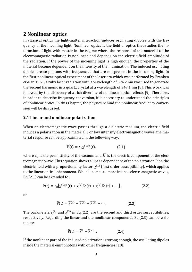
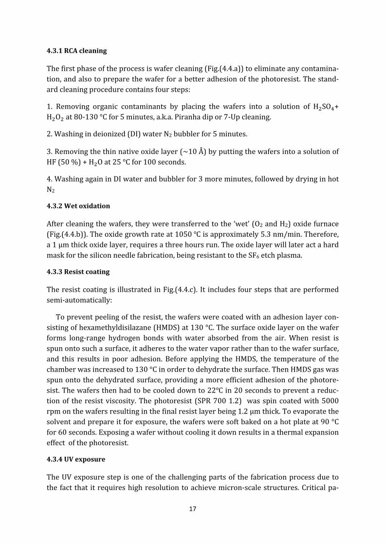
2.2Secondordernonlinearprocesses
The term ϵ χ E t in Eq.(2.2) describes the second order nonlinear interactions,whichareillustratedinFig.(2.1).
Figure 2.1 Second order nonlinear interaction processes.
Figure(2.1.a)showsthesecond‐harmonicgenerationprocess,wheretwoincidentpho‐tons,eachwithfrequencyω,arecombinedtogiveonenewphotonwithfrequency2ω.Theinducedpolarizationinthenonlinearmediumisthenasfollows:
P 2ϵ χ EE∗ ϵ χ E e c. c. .(2.5)
ThefirsttermofEq.(2.5)representsthezerofrequencycontribution,knownasopticalrectification. The second term represents the generated second‐harmonic signalwithfrequency2ω.Second‐harmonicgeneration is inpracticeuseful toaccess thespectralrangeofshorterwavelengths.
Figure (2.1.b) shows the case of sum‐frequency generation (SFG) and difference‐frequencygeneration(DFG).InSFG,twoincidentphotonswithfrequencies and propagatingthroughthenonlinearmediumarecombinedtocreataphotonwithhigherenergy, . In the DFG case, a lower energy photon is createdwith a fre‐quencyof (observethathere ).
Figure(2.1.c)showsanotherpossiblesecondordernonlinearinteractioncalledfre‐quency down‐conversion or optical parametric generation (OPG). Here, one photonwithfrequencyω propagatingthroughthenonlinearmediumissplitintotwophotonswithfrequenciesω andω repectively.Ifthenonlinearmediumisplacedinanopticalresonator,theconfigurationiscalledopticalparametricoscillator(OPO)[11].
2.3Susceptibilitycoefficient
Thenonlinearsusceptibilityisintroducedasatensorofrankm+1forχ ,but,usually,anonlinearcoefficient,d,isusedinsteadofχtensorandisdefinedinthefollowingway:
2 SHG
SFG, DFG
OPG, OPO
2 2
a
b
c
5
d χ .(2.6)
If the condition of permutation symmetry applies,d d , the d‐tensor can be ex‐
pressedasa3 6‐elementmatrix,andthepolarizationofthegeneratedphotonsinCar‐tesiancoordinatesisgivenbythecomponents:
P
P
P
2ϵ Kd d d d d dd d d d d dd d d d d d
E EE EE E
E E E EE E E EE E E E
, (2.7)
whereω is the frequencyof thegeneratedphotondue to theannihilationof thetwophotons with frequencies ω and ω . K is the degeneracy factor, given by K=½ ,whenω ω (SHGcase)andK=1whenω ω [12].
Consideringa second‐ordernonlinear interaction, the susceptibility coefficient χ onlyappearsincrystalswithoutacenterofinversion.Inmanymaterials,therefore,χ vanishesduetotheircentrosymetriccrystalstructure.
2.4Thecoupledwaveequation
Thenewfrequencycomponentsoftheelectromagneticfieldcanbeexpressedbyintro‐ducingawaveequation. If thenonlinearpart isaddedtothestandardwaveequation,onecanextractthecoupledwaveequationbetweentheinteractingwavesbythefollow‐ingexpression:
E μ σ μ ϵ μ ,(2.8)
whereμ isthevacuumpermeabilityandσistheconductivityofthecrystal.
Assumingawavepropagatinginthex‐direction.Inthesecondharmonicgenerationprocess,ittakestheformofplanewaves,E x, t ½ E x,ω e c. c,andwith
theapproximationofa slowlyvaryingelectric field, i.e. ≪ k , the threecoupled
equationsateachfrequency,canbederivedasfollowing:
α E Kd E E∗e ∆ ,
α E Kd E E∗e ∆ ,(2.9)
α E Kd E E∗e ∆ .
Here,d
ofthei
tioncobeingesity,the
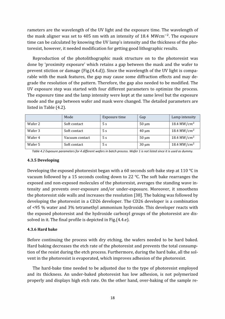
2.5Ph
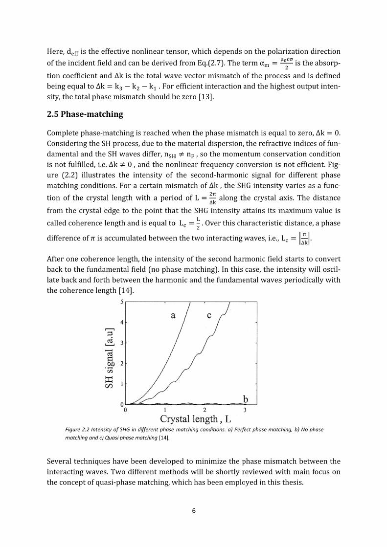
CompleConsiddamentisnotfure (2.matchi
tion of
fromth
calledc
differen
Afterobacktolatebacthecoh
Fig
m
Severalinteracthecon
d isthee
ncidentfie
efficientanequalto∆ketotalphas
hase‐matc
etephase‐meringtheStalandthefulfilled,i.e.2) illustrangconditio
f the crysta
hecrystale
coherencel
nceof isa
necoherenothefundackandfortherencelen
gure 2.2 Intens
atching and c)
ltechniquectingwavesnceptofqua
ffectiveno
eldandcan
nd∆kisthk k
semismatc
ching
matchingisSHprocess,eSHwavese.∆k 0,aates the intons.Forac
al lengthw
edgetothe
lengthand
accumulate
ncelength,amentalfielthbetweenngth[14].
sity of SHG in d
Quasi phase m
eshavebees.Twodiffeasi‐phasem
nlinearten
bederived
etotalwavk .For
chshouldb
sreachedwduetothediffer,nandthenontensity ofcertainmis
with a perio
epoint tha
isequalto
edbetween
theintensld(nophasntheharmo
different phase
atching [14].
endeveloperentmethmatching,w
6
nsor,which
dfromEq.(
vevectormefficientinbezero[13
whenthephemateriald
n ,sotnlinearfrethe seconsmatchof∆
od of L∆
at theSHG
oL .O
nthetwoin
sityofthessematchinonicandth
matching cond
pedtominihodswillbwhichhasb
hdependso
(2.7).Thet
mismatchonteractiona].
hasemismdispersion,themomenquencycond‐harmoni∆k,theSH
∆ along th
intensitya
verthisch
nteractingw
secondharng).Inthishefundame
ditions. a) Perfe
imizethepeshortlyrbeenemplo
, L
onthepola
ermα
oftheprocandthehig
atchisequtherefractntumconsenversionisc signal foHGintensity
he crystal a
attains itsm
aracteristic
waves,i.e.,
monicfieldcase,theinentalwaves
ect phase matc
phasemismeviewedwoyedinthis
arizationd
isthe
essandisghestoutpu
ualtozero,tiveindiceservationcosnotefficieor differenyvariesas
axis. The d
maximumv
cdistance,
L∆.
dstartstontensitywisperiodica
ching, b) No ph
matchbetwwithmainfsthesis.
irection
absorp‐
definedutinten‐
∆k 0.soffun‐onditionent.Fig‐t phaseafunc‐
distance
value is
aphase
convertilloscil‐allywith
hase
weenthefocuson

7
2.5.1Birefringentphase‐matchingandquasi‐phasematching
Thereareseveraltechniquesforcompensatingthephasemismatchinthecrystal.Onetechnique takesadvantageof thenaturalbirefringenceof themediumitself. Thebire‐fringenceisdefinedasthedifferencebetweentherefractiveindicesoftheordinaryandthe extraordinary wave defined on the principal axis of the crystal. In birefringentphase‐matching, by choosing a specific “cut” or crystal orientation, the interactingwavesexperiencethesamerefractiveindices.Consequently,theypropagateatthesamephasevelocityand∆kisthuszero.Growth,preparationandalignmentofthesecrystalsis straightforward. However, the applicability of simple birefringent phase‐matchingcan be limited by a number of factors. First, since themethod relies on thematerialproperties(thedispersionandthebirefringence),findingacrystalorientationthatsat‐isfiesthephase‐matchingconditionischallenging.Second,thenonlinearitydependsonthepropagationdirectioninthecrystal.
Anotherphasematchingtechnique,whichisbasedonthecompensationofphaseve‐locity differences between the interacting waves, is quasi‐phase matching (QPM). InQPM, thesignof thenonlinearsusceptibility ismodulated in thespatial coordinate topreventaccumulationofphasemismatch.Suchaspatialmodulationcanbeobtainedinferroelectriccrystalsbyperiodicallyalteringthecrystalorientationandinthiswaytheeffective nonlinearity changes between d and d . The interacting waves stillpropagatewithdifferentphasevelocities,but,whentheaccumulatedphasemismatchreachesπ, the sign of the drivingnonlinear susceptibility is also reversed so that thephasedifference isreset tozero.Thiscreatesastep‐wisegrowthintheoutputpoweralongthecrystallengthascanbeseeninFigure2.2.c.Ideally,themodulationisdoneaf‐tereachcoherence length,L , and is referredtoas the first‐orderQPM.OnecanalsousehigherorderQPMwherethematerialismodulatedwithaperiodofseveralcoher‐encelengths.Besidesahigherefficiency,QPMstructurescanbemadewithanyperiodandstructureaswell asprovidephasematching foranynonlinearprocess inside thetransparencywindowofthematerial[15].
InaQPMstructure,theperiodicallymodulatednonlinearcoefficientisusedtocom‐pensateforthephasemismatchinthecrystal.Thisnonlinearcoefficient, ,canbewrit‐teninthespatialcoordinatebyaFourierexpansion:
d x d ∑ G exp ik x ,(2.10)
whered isthenonlinearcoefficient,k isthem ordergratingvectorwhichsatisfies
thephase‐matchingcondition,andG istheFouriercoefficientofthem harmonicde‐finedas[16]:
G sin mπD .(2.11)
Here,Disthedutycycle,whichisdeterminedbytheratioofthereverseddomainlengthand the structure period. From Eq.(2.11) it follows that the most efficient phase‐
8
matchingwillbe for the firstorderQPM(m=±1)andwithaduty‐cycleof50%(D=1/2). Whereas for second‐order QPM, efficient phase‐matching is gained for a duty‐cycleof25%(D=1/4).
2.5.2Quasi‐phasematchedsecond‐harmonicgenerator
ThewavevectormismatchforQPMSHGcanbewrittenas:
Δk k 2k k ,(2.12)
wherek ,thesocalledm harmonicgratingvector,isdefinedas:
k .(2.13)
When theSHGand the fundamentalwavesarequasi‐phasematched, i.e.,Δk 0, the
gratingstructureperiodcanbewrittenas:
Λ 1,2,3, ….(2.14)
Thelengthofthegratingstructurecanthenbeadjustedformaximizingtype‐Iandtype‐IIQPMSHGprocesses.Type‐Iandtype‐IISHGarerelatedtod andd ,respectively.
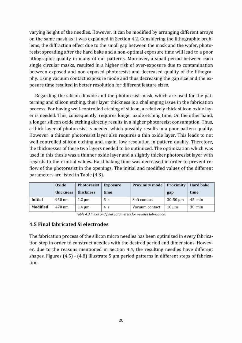
2.6FabricationmethodsofQPMstructures
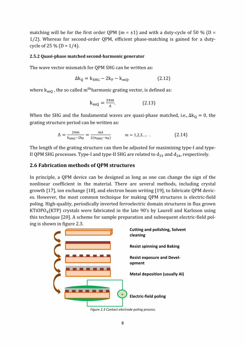
Inprinciple, aQPMdevice canbedesigned as long as one can change the signof thenonlinear coefficient in the material. There are several methods, including crystalgrowth[17],ionexchange[18],andelectronbeamwriting[19],tofabricateQPMdevic‐es.However, themost common technique formakingQPM structures is electric‐fieldpoling.High‐quality,periodicallyinvertedferroelectricdomainstructuresinfluxgrownKTiOPO (KTP) crystalswere fabricated in the late90’sbyLaurell andKarlssonusingthistechnique[20]. Aschemeforsamplepreparationandsubsequentelectric‐fieldpol‐ingisshowninfigure2.3.
Figure 2.3 Contact electrode poling process.
V
Cutting and polishing, Solvent cleaning
Resist spinning and Baking
Resist exposure and Devel‐opment Metal deposition (usually Al)
Electric‐field poling
9
Theferroelectriccrystaliscutintosmallpiecesandthec‐faceispolishedtoprovideoptimum light beampropagation. After cleaning the samples, the photoresist is spin‐coatedonthepolarfacesofeachcrystal.Theperiodicstructureiscreatedbyastandardphotolithographicprocess.Finally,metalelectrodesareformedbymet‐aldepositionontopofthephotoresist.Thelaststepisapplyingavoltageacrossthecrystaltocreatethedomainsofreversedpolarizationunderthemetalelectrodes.
TheQPMdeviceshavea veryhighefficiency,when thedomain structures areuni‐formthroughoutthewholethicknessofthecrystalaswellasinthedirectionoftheop‐ticalbeampropagation. Fabricationofperiodically‐poled crystals canbedoneonly incertain crystalmaterials. Thesematerials are ferroelectric nonlinear crystals such asKTP, LiNbO andLiTaO .
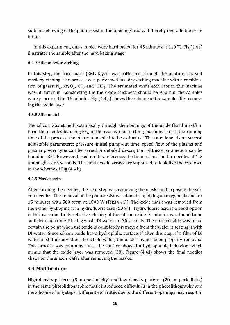
2.71Dand2Dquasi‐phasematchedcrystals
For1DQPM,theincidentplanewaveisusuallypropagatinginthex‐directionandthephasemismatchcanbecompensatedforinastructurewiththeperiodΛ,whichisequal
toamultipleofthefundamentalspatialfrequencyofthestructure, .Ina2Dcrystal,
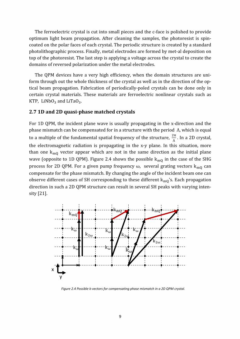
the electromagnetic radiation is propagating in the x‐y plane. In this situation, morethan one k vector appearwhich are not in the same direction as the initial planewave(oppositeto1DQPM).Figure2.4showsthepossiblek inthecaseoftheSHGprocess for2DQPM.Foragivenpump frequencyω, severalgratingvectorsk cancompensateforthephasemismatch.BychangingtheangleoftheincidentbeamonecanobservedifferentcasesofSHcorrespondingtothesedifferentk ’s.Eachpropagationdirectioninsucha2DQPMstructurecanresultinseveralSHpeakswithvaryinginten‐sity[21].
Figure 2.4 Possible k‐vectors for compensating phase mismatch in a 2D QPM crystal.
x
y
k
k
k
k
k
k
k
k
k
k
k
k
3KTPImplemlarizatifulfilledandsecoftheisities,cquencysizeoftanylpdamageshownwhileRischose
3.1Cry
Thecryb=6.3graphicneouspsistsofconsistchannetodomarelocarahedraK ions
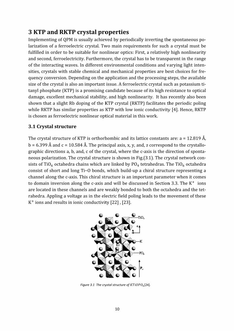
PandRmentingofQionofa ferdinordertcond,ferrointeractingcrystalswityconversiothecrystalhosphate(e,excellentthatasligRKTPhassenasferro
ystalstru
ystalstruct99 andccdirectionpolarizatiofTiO octahtofshortaelalongthemaininversiatedinthea.Applingsandresul
RKTPcryQPMisusurroelectrictobesuitaelectricity.gwaves.Inthstablechon.Dependiisalsoan(KTP)isaptmechanichtRbdopiimilarpropelectricno
ucture
tureofKTP=10.584sa,b,and,n.ThecryshedrachainandlongTiec‐axis. Thionalongtesechannelavoltageatsinionicc
Fig
ystalprouallyachievcrystal.TwblefornonFurthermodifferentehemicalaningontheaimportantpromisingccalstabilityingoftheKpertiesasKnlinearopt
Pisorthorh.Theprincofthecrstalstructunswhicha−Obonds,ischiralstrthec‐axisalsandarewasintheeleconductivit
ure 3.1 The cry
10
opertiesvedbyperiwomainrenlinearoptore,thecryenvironmenndmechaniapplicationissue.Afercandidateby,andhighKTPcrystaKTPwithlticalmater
hombicandncipalaxis,rystal,wheureisshowrelinkedbwhichbuiructureisaandwillbeweaklybonectricfieldty[22],[23
ystal structure o
siodicallyinequirementtics:First,aystalhastontalconditicalpropernandtheprrroelectricbecauseofnonlineari
al(RKTP)faowioniccoialinthisw
ditslatticex,y,and,zrethec‐ax
wninFig.(3.byPO tetrld‐upachianimportaediscussedndedtobotpolinglea3].
of [24
nvertingthets forsucharelativelyobetranspionsandvartiesareberocessingscrystalsucitshighreity. Ithasracilitatesthonductivitywork.
econstantscorresponxisisthedi.1). Thecryahedras.ThiralstructuantparameinSectionththeoctadstothem
4].
espontaneacrystalm
yhighnonlparentinthvaryinglighestchoicessteps,theavchaspotasesistancetorecentlyalheperiodicy[4].Hence
are:a=12ndtothecrirectionofystalnetwoheTiO ocurerepreseeterwhenin3.3.TheKahedraandmovemento
eouspo‐mustbeinearityherangehtinten‐forfre‐vailablesiumti‐oopticalsobeencpolinge,RKTP
2.819 ,rystallo‐sponta‐orkcon‐tahedraentingatcomesK ionsthetet‐ofthese
11
Thenonlinearopticalmaterialwhich ischosen for thisproject is KTPclosestrela‐tive,Rb‐dopedKTP,RKTP.InRKTPcrystal,the ionsaresubstitutedby ions.TheRKTPcrystalhassimilarpropertiesasKTPwithlessionicconductivity.
3.2Crystalproperties
Ferroelectricity
Ferroelectric crystals are materials with spontaneous polarization, which can beswitchedbetween twoopposing statesbyapplying anelectric field. The spontaneouspolarizationisdefinedbythecompositionofnegativeandpositiveions.Inequilibrium,thecenterofpositiveandnegativeionsdoesnotcoincide.Therefore,eachpairofnega‐tiveandpositiveionscanbeconsideredasanelectricdipole.Thesumoftheseindividu‐aldipoleswiththesamedirectionconstitutesthespontaneouspolarization.Anyregionofaferroelectriccrystalwithuniformspontaneouspolarizationiscalledadomain.Theinterfaceborderbetweeneachdomaininsidethecrystaliscalleddomainwall.ForKTPandRKTP, thedomains areorientedalong the c‐ direction forming the180 ° domainwallsbetweenthem.Thedomainwallsareparalleltothe100crystalplane[25],[26].
Ionicconductivity
Ionicconductivityplaysan importantrole fortheprocessofdomainswitching inKTPcrystals.ThenatureoftheKTPmaterialallowsthediffusionofatomsinthestructure.Undercertainthermalconditions,thepotassiumions(K )tendtohopoverthevacan‐ciesandtherebyintroducinganionicconductivityinthec‐axisdirection.Theconductiv‐ityalongthepolaraxiscanbeuptofourordersofmagnitudelargerthanthedirectionperpendiculartothepolaraxis[25].Highionicconductivitycauseslargecurrenttoflowthroughthecrystalwhenahighvoltageisapplied;thiscanresultinelectricaldamagesofthecrystal[27].InordertodecreasetheionicconductivityoftheKTPcrystal,onecanintroduceadopantlikeRb.SinceRb hasalargerradiusthanK ,itismoredifficultfortheRb topassthroughtheconductivitychannelsinRKTP.TheRb alsoblocksthelat‐ticeforthemovementofthemajorityoftheK ions,whichotherwisewouldhopfromsite to site.This isnotpossible, since theneighboringspacesarealreadyoccupiedbyRb .ThehoppingrateofK isthenreducedwithrespecttothatofRb astherearenopossibilities for theK ion topass theRb ion [28]. The ionic conductivity ofRKTP istypicallyabout2ordersofmagnitudelowerthanthatofflux‐grownKTP[29].
3.3Domainswitching
Nonlinear crystals such as KTP, which are used for QPM frequency conversion, aregrowntohaveonesingledomainandarecutalonga,bandtheccrystallographicaxes.Inordertoalterthepolarization,theappliedelectricfieldmustexceedacertainthresh‐old,calledcoercivefield.Thevalueofthecoercivefielddependsonparameterssuchasthe frequency, thewaveformof theappliedvoltage, thetemperatureandtheshapeofthecontactelectrode.

12
Ferroelectricdomain inversionbycontactpoling, isbasedonthreesteps.First,nu‐cleationofthedomainwhichstarts fromtheedgeofeachelectrodewherethefield isstrongest.Second,thedomainwillrapidlypropagatesforwardalongthepolardirectionofthecrystalandatthesametime,thedomainwillslowlygrowssideways[30].Nucle‐ationistheformationofsmallantiparalleldomainsundercontactelectrodesinsidethecrystal,which grow and subsequentlymerge together. These domains can growbothalongtheferroelectricaxisorbysidewaysmotion. It isestimatedthat inKTP,thedo‐main‐wall growth velocity in the polar direction is, at least, two orders ofmagnitudelargerthaninthex‐yplane.Thevelocityalongthey‐axisisaround30timeslargerthanthatalongthex‐axisduetothecrystalstructureofKTP[31].Domainmovementinthesidewaysdirectionsisnotdesiredinelectricfield‐poling,sinceitcausesdeviationfromtheidealdutycycle,domainmergings,andwillruinthegratingquality.
4Sili
Siliconbecontobservtallinemancequired
4.1Me
Theree[32], wmasksflexible(heightthenee
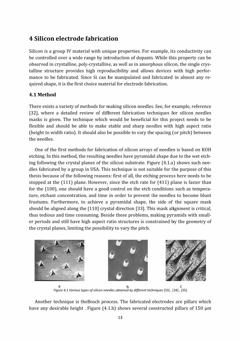
Oneetchingingfolldlesfabthesisbstoppedfortheture,etfrustumshouldthusteerperithecry
Anothavean
iconelec
isagrouptrolledoveedincryststructureto be fabrshape,itis
ethod
existsavarwhere a deis given. Te and shouttowidthredles.
ofthefirstg.Inthismelowingthebricatedbybecauseofdatthe(1(100),onetchantconcms. Furthebealigneddiousandodsandstiystalplanes
Figure 4
ther technnydesirab
a
ctrodef
IVmateriaerawideraalline,polyprovides hricated. Sinsthefirstch
rietyofmetetailed reviThe techniquld be ableratio).Itsh
tmethodsethod,thecrystalplayagroupinthefollowi111)plane.eshouldhacentration,rmore, todalongthetimeconsuillhavehigs,limitingth
4.1 Various type
ique is theleheight .
fabricat
alwithuniangebyinty‐crystallinhigh repronce Si canbhoicemate
thodsformiew of diffquewhiche tomakehouldalsob
forfabricaresultingnanesofthenUSA.ThisingreasonsHowever,aveagood,andtimeachieve a[110]crysuming.Besighaspectrhepossibil
es of silicon nee
eBoschproFigure(4.1
13
tion
iquepropetroductione,aswellaoducibilitybemanipuerialforele
makingsilicferent fabrwould bestable andbepossible
ationofsilineedleshavsiliconsubstechniques:firstofasincethee
dcontroloninordertopyramida
staldirectioidethesepratiostructitytovary
edles obtained b
ocess.The f1.b)shows
b
rties.Foreofdopantsasinamorpand allowlated andctrodefabr
conneedlesrication tecbeneficiald sharp neeetovaryth
iconarraysvepyramidbstrate.Figeisnotsuiall,theetchetchratefontheetchoprevent tl shape, thon[33].Thproblems,muresisconthepitch.
by different tech
fabricatedsseveralco
example,itss.Whilethiphoussilicos devices wfabricatedrication.
s.See,forechniques fofor this predleswithespacing(
sofneedlesalshapedugure(4.1.a)itableforthingprocessor(411)plconditionstheneedleshe side ofismaskalimakingpyrnstrainedb
hniques [33] , [3
electrodesonstructed
sconductivispropertyon,thesingwith highin almost
example,reor siliconroject needhigh aspe(orpitch)b
sisbaseduetothew)showssuhepurposeshereneedlaneisfastssuchastes tobecomthe squarignmentisramidswithbythegeom
34] , [35].
sarepillarpillarsof
c
vitycanycanbeglecrys‐perfor‐any re‐
eferenceneedlesds to beect ratiobetween
onKOHwetetch‐uchnee‐eofthisdstobeterthanempera‐mebluntre maskcritical,hsmall‐metryof
swhich150µm
heightenoughenoughThe
termedduringdeeplyshownanoptitainevdles,aofbreaRega
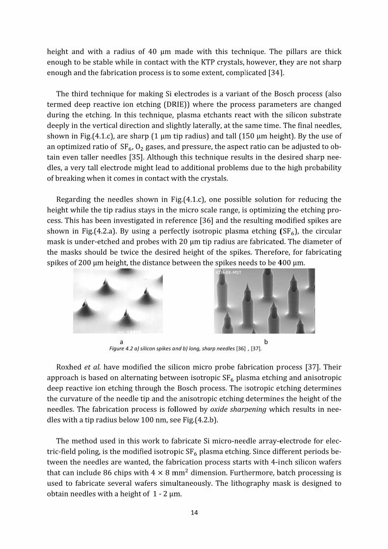
heightcess.Thshownmaskisthemaspikes
RoxhapproadeeprethecurneedlesdleswiThe
tric‐fieltweentthatcaused toobtain
and withhtobestabhandthefa
thirdtechddeep reactheetchininthevertinFig.(4.1mizedratioventallernverytallelakingwhen
arding thewhilethethishasbeein Fig.(4.2sunder‐etcasks shouldof200µm
hedetal.hachisbasedeactiveionrvatureofts.The fabrithatiprad
methodusldpoling,istheneedleninclude8o fabricateneedleswi
a radius oblewhileinabricationp
niqueformctive ion etng. In this tticaldirecti.c),areshaoofSF ,Oeedles[35lectrodemitcomesin
needles shtipradiusseninvestiga2.a). By usichedandpdbe twiceheight,the
Figure 4.2 a)
havemodifdonalternnetchingththeneedlericationprodiusbelow
sedinthissthemodifsarewant86chipswiseveralwithaheight
a
of 40 µm mncontactwprocessist
makingSietching (DRtechnique,ionandsligarp(1µmtgases,an].Althoughightleadtoncontactw
hown in Fstaysintheatedinrefeing a perferobeswiththedesiredistanceb
silicon spikes an
fied the silatingbetwhroughthetipandtheocess is fol100nm,se
worktofafiedisotropted,thefabith4 8m
wafers simutof1‐2µm
14
made withwiththeKTtosomeext
electrodesRIE))wherplasmaetcghtlylateratipradius)ndpressurehthistechnoadditionawiththecry
ig.(4.1.c), oemicroscaerence[36ectly isotroh20µmtipedheight obetweenthe
nd b) long, sha
liconmicroweenisotroBoschproeanisotropllowedbyeeFig.(4.2.b
abricateSipicSF plasbricationprmm dimenultaneouslym.
h this techPcrystals,tent,compl
isavariane theprocchants reaally,atthesandtall(1e,theaspecniqueresualproblemystals.
one possibalerange,is]andtheropic plasmapradiusareof the spikeespikesne
rp needles [36]
oprobe fabpicSF plaocess.Theipicetchingoxidesharpb).
micro‐neesmaetchinrocessstarnsion.Furthy. The litho
nique. Thehowever,tlicated[34]
ntoftheBoessparamectwith thesametime.50µmheigtratiocanltsinthedsduetoth
le solutionsoptimizinresultingma etching (efabricatedes.Therefoeedstobe4
, [37].
bricationpasmaetchinisotropicetdeterminepeningwhi
edlearray‐eg.Sincediftswith4‐inhermore,bographyma
b
e pillars artheyareno].
oschproceeters are ce silicon su.Thefinalnght).Bythbeadjustedesiredshahehighpro
n for reducngtheetchimodifiedspi(SF ), thed.Thediamore, for fab400µm.
process [37ngandanistchingdetestheheighichresults
electrodeffferentperinchsiliconbatchproceask is desi
re thickotsharp
ss(alsochangedubstrateneedles,euseofdtoob‐arpnee‐bability
cing theingpro‐ikesarecircularmeterofricating
7].Theirsotropicermineshtoftheinnee‐
forelec‐iodsbe‐nwafersessingisgned to
15
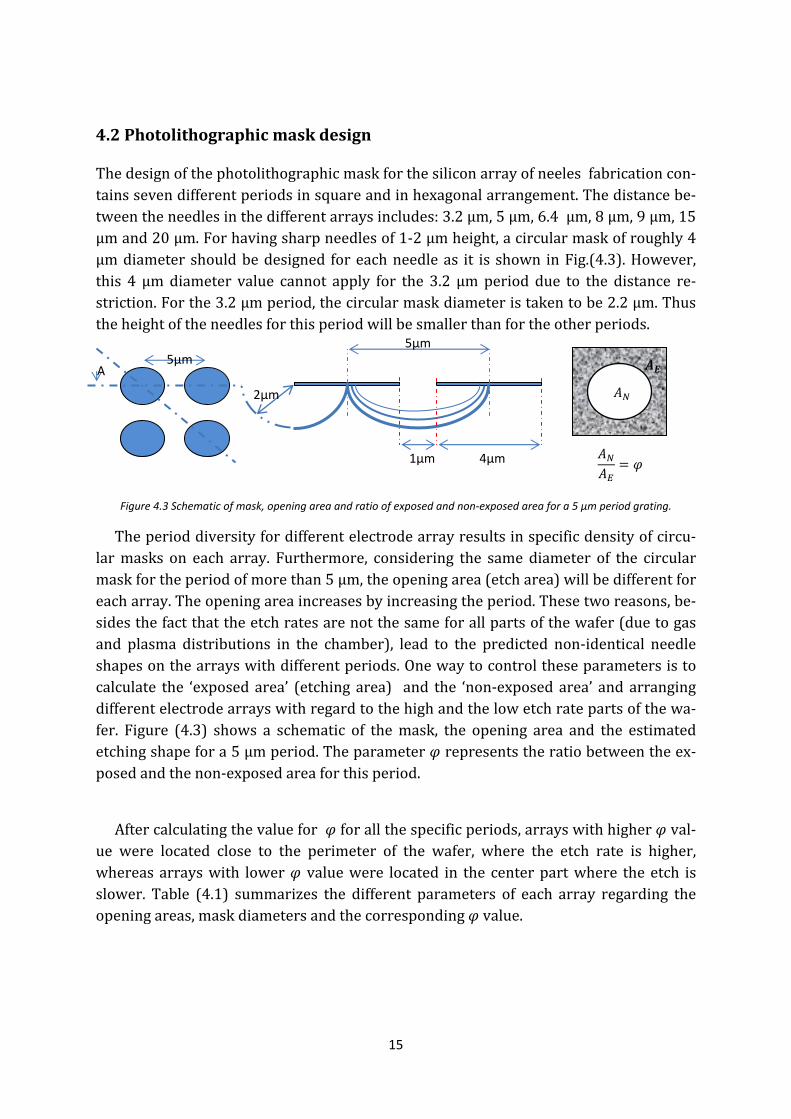
4.2Photolithographicmaskdesign
Thedesignofthephotolithographicmaskforthesiliconarrayofneelesfabricationcon‐tainssevendifferentperiodsinsquareandinhexagonalarrangement.Thedistancebe‐tweentheneedlesinthedifferentarraysincludes:3.2µm,5µm,6.4µm,8µm,9µm,15µmand20µm.Forhavingsharpneedlesof1‐2µmheight,acircularmaskofroughly4µmdiameter shouldbedesigned foreachneedleas it is shown inFig.(4.3).However,this 4 µmdiameter value cannot apply for the 3.2 µmperiod due to the distance re‐striction.Forthe3.2µmperiod,thecircularmaskdiameteristakentobe2.2µm.Thustheheightoftheneedlesforthisperiodwillbesmallerthanfortheotherperiods.
Figure 4.3 Schematic of mask, opening area and ratio of exposed and non‐exposed area for a 5 µm period grating.
Theperioddiversityfordifferentelectrodearrayresultsinspecificdensityofcircu‐larmasks on each array. Furthermore, considering the same diameter of the circularmaskfortheperiodofmorethan5µm,theopeningarea(etcharea)willbedifferentforeacharray.Theopeningareaincreasesbyincreasingtheperiod.Thesetworeasons,be‐sidesthefactthattheetchratesarenotthesameforallpartsofthewafer(duetogasand plasma distributions in the chamber), lead to the predicted non‐identical needleshapesonthearrayswithdifferentperiods.Onewaytocontroltheseparametersistocalculate the ‘exposedarea’ (etching area) and the ‘non‐exposed area’ and arrangingdifferentelectrodearrayswithregardtothehighandthelowetchratepartsofthewa‐fer. Figure (4.3) shows a schematic of themask, the opening area and the estimatedetchingshapefora5µmperiod.Theparameter representstheratiobetweentheex‐posedandthenon‐exposedareaforthisperiod.
Aftercalculatingthevaluefor forallthespecificperiods,arrayswithhigher val‐ue were located close to the perimeter of the wafer, where the etch rate is higher,whereasarrayswith lower valuewere located in the centerpart where theetch isslower. Table (4.1) summarizes the different parameters of each array regarding theopeningareas,maskdiametersandthecorresponding value.
5µm A
5µm
4µm1µm
2µm
16
Period (µm) Type Mask diameter (µm) : Non‐exposed area : Exposed area ⁄
3.2 Hexagonal 2.2 3.73 5.02 0.74
Square 2.2 3.73 6.38 0.58
5 Hexagonal 4 12.56 9.09 1.38
Square 4 12.56 12.44 1.01
6.4 Hexagonal 4 12.56 22.86 0.55
Square 4 12.56 28.44 0.44
8 Hexagonal 4 12.56 42.64 0.29
Square 4 12.56 51.44 0.24
9 Hexagonal 4 12.56 59.14 0.21
Square 4 12.56 70.25 0.18
15 Hexagonal 4 12.56 182.2 0.07
Square 4 12.56 212.44 0.06
20 Hexagonal 4 12.56 333.85 0.04
Square 4 12.56 387.44 0.03
Table 4.1 Mask diameter, exposed and non‐exposed areas for different gratings on the wafer.
Althoughthearrangementof thearrayswasdone to get the same result in all cases, alargedifferenceinthe valueleadtoantici‐pateddifferentneedleshapes.Comment:Theless exposed area open to the etch gasesthereisonthewafer,themoreuniformetchresultswillyield(duetolessconsumptionofetch‐gasmoleculesandthusamorehomoge‐nous etch plasma with less excausted vol‐umes). In reality, very low :s areunpracti‐cal, as you get very few etched features onyourwafer.
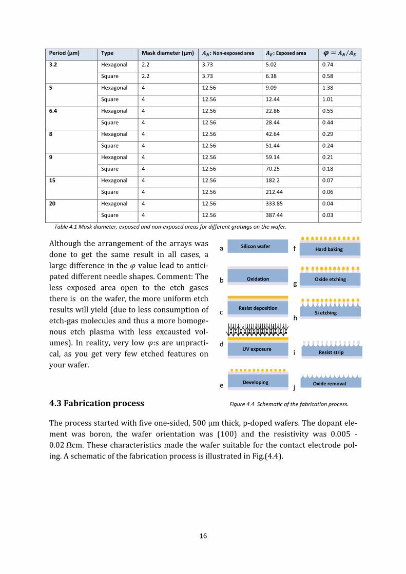
4.3Fabricationprocess Figure 4.4 Schematic of the fabrication process.
Theprocessstartedwithfiveone‐sided,500µmthick,p‐dopedwafers.Thedopantele‐ment was boron, the wafer orientation was (100) and the resistivity was 0.005 ‐0.02Ωcm.Thesecharacteristicsmadethewafersuitable forthecontactelectrodepol‐ing.AschematicofthefabricationprocessisillustratedinFig.(4.4).
Silicon wafer
a
b
c
d
e
f
g
h
i
j
Oxidation
Resist deposition
UV exposure
Developing
Hard baking
Oxide etching
Si etching
Resist strip
Oxide removal
17
4.3.1RCAcleaning
Thefirstphaseoftheprocessiswafercleaning(Fig.(4.4.a))toeliminateanycontamina‐tion,andalsotopreparethewaferforabetteradhesionofthephotoresist.Thestand‐ard cleaningprocedurecontainsfoursteps:
1. Removing organic contaminants by placing the wafers into a solution of H SO +H O at80‐130°Cfor5minutes,a.k.a.Piranhadipor7‐Upcleaning.
2.Washingindeionized(DI)waterN2bubblerfor5minutes.
3.Removingthethinnativeoxidelayer(~10 )byputtingthewafersintoasolutionofHF(50%)+H Oat25°Cfor100seconds.
4.WashingagaininDIwaterandbubblerfor3moreminutes,followedbydryinginhotN2
4.3.2Wetoxidation
Aftercleaningthewafers,theyweretransferredtothe‘wet’(O2andH2)oxidefurnace(Fig.(4.4.b)).Theoxidegrowthrateat1050 isapproximately5.3nm/min.Therefore,a1µmthickoxidelayer,requiresathreehoursrun.Theoxidelayerwilllateractahardmaskforthesiliconneedlefabrication,beingresistanttotheSF6etchplasma.
4.3.3Resistcoating
Theresistcoating is illustratedinFig.(4.4.c). It includesfourstepsthatareperformedsemi‐automatically:
Topreventpeelingoftheresist,thewaferswerecoatedwithanadhesionlayercon‐sistingofhexamethyldisilazane(HMDS)at130°C.Thesurfaceoxidelayeronthewaferforms long‐range hydrogen bonds with water absorbed from the air. When resist isspunontosuchasurface,itadherestothewatervaporratherthantothewafersurface,and this results in poor adhesion. Before applying theHMDS, the temperature of thechamberwasincreasedto130°Cinordertodehydratethesurface.ThenHMDSgaswasspunontothedehydratedsurface,providingamoreefficientadhesionofthephotore‐sist.Thewafersthenhadtobecooleddownto22 in20secondstopreventareduc‐tionof theresistviscosity.Thephotoresist (SPR7001.2) wasspincoatedwith5000rpmonthewafersresultinginthefinalresistlayerbeing1.2µmthick.Toevaporatethesolventandprepareitforexposure,thewafersweresoftbakedonahotplateat90°Cfor60seconds.Exposingawaferwithoutcoolingitdownresultsinathermalexpansioneffectofthephotoresist.
4.3.4UVexposure
TheUVexposurestepisoneofthechallengingpartsofthefabricationprocessduetothefactthat itrequireshighresolutiontoachievemicron‐scalestructures.Criticalpa‐
18
rametersarethewavelengthoftheUVlightandtheexposuretime.Thewavelengthofthemaskalignerwassetto405nmwithan intensityof18.4MWcm .TheexposuretimecanbecalculatedbyknowingtheUVlamp’sintensityandthethicknessofthepho‐toresist,however,itneededmodificationforgettinggoodlithographicresults.
Reproduction of the photolithographic mask structure on to the photoresist wasdoneby ‘proximityexposure’whichretainsagapbetweenthemaskandthewafer topreventstictionordamage(Fig.(4.4.d)).SincethewavelengthoftheUVlightiscompa‐rablewith themask features, thegapmaycausesomediffractioneffectsandmayde‐gradetheresolutionofthepattern.Therefore,thegapalsoneededtobemodified.TheUVexposurestepwasstartedwith fourdifferentparameters tooptimize theprocess.Theexposuretimeandthelampintensitywerekeptatthesamelevelbuttheexposuremodeandthegapbetweenwaferandmaskwerechanged.ThedetailedparametersarelistedinTable(4.2).
Mode Exposuretime Gap Lampintensity
Wafer2 Softcontact 5 s 50 µm 18.4MW/
Wafer3 Softcontact 5 s 40 µm 18.4MW/
Wafer4 Vacuumcontact 5 s 50 µm 18.4MW/
Wafer5 Softcontact 5 s 30 µm 18.4MW/
Table 4.2 Exposure parameters for 4 different wafers in batch process. Wafer 1 is not listed since it is used as dummy.
4.3.5Developing
Developingtheexposedphotoresistbeganwitha60secondssoft‐bakestepat110 invacuumfollowedbya15secondscoolingdownto22 .Thesoftbakerearrangestheexposedandnon‐exposedmoleculesofthephotoresist,averagesthestandingwavein‐tensity and prevents over‐exposure and/or under‐exposure. Moreover, it smoothensthephotoresistsidewallsandincreasestheresolution[38].ThebakingwasfollowedbydevelopingthephotoresistinaCD26developer.TheCD26developerisacombinationof<95%waterand3%tetramethylammoniumhydroxide.Thisdeveloperreactswiththeexposedphotoresistandthehydroxidecarboxylgroupsofthephotoresistaredis‐solvedinit.ThefinalprofileisdepictedinFig.(4.4.e).
4.3.6Hardbake
Before continuing theprocesswith dry etching, thewafers needed to be hardbaked.Hardbakingdecreasestheetchrateofthephotoresistandpreventsthetotalconsump‐tionoftheresistduringtheetchprocess.Furthermore,duringthehardbake,allthesol‐ventinthephotoresistisevaporated,whichimprovesadhesionofthephotoresist.
Thehard‐baketimeneededtobeadjustedduetothetypeofphotoresistemployedand its thickness. An under‐baked photoresist has low adhesion, is not polymerizedproperlyanddisplayshighetchrate.Ontheotherhand,over‐bakingofthesamplere‐
19
sultsinreflowingofthephotoresistintheopeningsandwilltherebydegradethereso‐lution.
Inthisexperiment,oursampleswerehardbakedfor45minutesat110 .Fig.(4.4.f)illustratesthesampleafterthehardbakingstage.
4.3.7Siliconoxideetching
In this step, the hardmask (SiO layer) was patterned through the photoresists softmaskbyetching.Theprocesswasperformedinadry‐etchingmachinewithacombina‐tionof gases:N ,Ar,O , CF andCHF .Theestimatedoxideetch rate in thismachinewas 60 nm/min. Considering the the oxide thickness should be 950 nm, the sampleswereprocessedfor16minutes.Fig.(4.4.g)showstheschemeofthesampleafterremov‐ingtheoxidelayer.
4.3.8Siliconetch
Thesiliconwasetched isotropically throughtheopeningsof theoxide(hardmask)toformtheneedlesbyusingSF in thereactive ionetchingmachine.Toset therunningtimeoftheprocess,theetchrateneededtobeestimated.Theratedependsonseveraladjustableparameters: pressure, initial pump‐out time, speed flowof theplasmaandplasma power type can be varied. A detailed description of these parameters can befoundin[37].However,basedonthisreference,thetimeestimationforneedlesof1‐2µmheightis65seconds.ThefinalneedlearraysaresupposedtolooklikethoseshownintheschemeofFig.(4.4.h).
4.3.9Masksstrip
Afterformingtheneedles,thenextstepwasremovingthemasksandexposingthesili‐conneedles.Theremovalofthephotoresistwasdonebyapplyinganoxygenplasmafor15minuteswith500sccmat1000W(Fig.(4.4.i)).Theoxidemaskwasremovedfromthewaferbydippingitinhydrofluoricacid(50%).Hydrofluoricacidisagoodoptioninthiscaseduetoitsselectiveetchingofthesiliconoxide.2minuteswasfoundtobesufficientetchtime.RinsingwasinDIwaterfor30seconds.Themostreliablewaytoas‐certainthepointwhentheoxideiscompletelyremovedfromthewaferistestingitwithDIwater.Sincesiliconoxidehasahydrophilicsurface, ifafter thisstep, ifa filmofDIwater is stillobservedon thewholewafer, theoxidehasnotbeenproperly removed.This processwas continued until the surface showed a hydrophobic behavior,whichmeans that the oxide layer was removed [38]. Figure (4.4.j) shows the final needlesshapeonthesiliconwaferafterremovingthemasks.
4.4Modifications
High‐densitypatterns(5µmperiodicity)andlow‐densitypatterns(20µmperiodicity)inthesamephotolithographicmaskintroduceddifficultiesinthephotolithographyandthesiliconetchingsteps.Differentetchratesduetothedifferentopeningsmayresultin
20
varyingheightoftheneedles.However,itcanbemodifiedbyarrangingdifferentarraysonthesamemaskasitwasexplainedinSection4.2.Consideringthelithographicprob‐lems,thediffractioneffectduetothesmallgapbetweenthemaskandthewafer,photo‐resistspreadingafterthehardbakeandanon‐optimalexposuretimewillleadtoapoorlithographic quality inmany of our patterns.Moreover, a small period between eachsinglecircularmasks,resulted inahigherriskofover‐exposuredue tocontaminationbetween exposed andnon‐exposedphotoresist anddecreasedquality of the lithogra‐phy.Usingvacuumcontactexposuremodeandthusdecreasingthegapsizeandtheex‐posuretimeresultedinbetterresolutionfordifferentfeaturesizes.
Regardingthesilicondioxideandthephotoresistmask,whichareusedforthepat‐terningandsiliconetching,theirlayerthicknessisachallengingissueinthefabricationprocess.Forhavingwell‐controlledetchingofsilicon,arelativelythicksiliconoxidelay‐erisneeded.This,consequently,requireslongeroxideetchingtime.Ontheotherhand,alongersiliconoxideetchingdirectlyresultsinahigherphotoresistconsumption.Thus,a thick layerofphotoresist isneededwhichpossiblyresults inapoorpatternquality.However,athinnerphotoresistlayeralsorequiresathinoxidelayer.Thisleadstonotwell‐controlledsiliconetchingand,again, lowresolutioninpatternquality.Therefore,thethicknessesofthesetwolayersneededtobeoptimized.Theoptimizationwhichwasusedinthisthesiswasathinneroxidelayerandaslightlythickerphotoresistlayerwithregardstotheirinitialvalues.Hardbakingtimewasdecreasedinordertopreventre‐flowofthephotoresistintheopenings.TheinitialandmodifiedvaluesofthedifferentparametersarelistedinTable(4.3).
Oxide
thickness
Photoresist
thickness
Exposure
time
Proximitymode Proximity
gap
Hardbake
time
Initial 950nm 1.2µm 5 s Softcontact 30‐50µm 45min
Modified 470nm 1.4µm 4 s Vacuumcontact 10µm 30min
Table 4.3 Initial and final parameters for needles fabrication.
4.5FinalfabricatedSielectrodes
Thefabricationprocessofthesiliconmicroneedleshasbeenoptimizedineveryfabrica‐tionstepinordertoconstructneedleswiththedesiredperiodanddimensions.Howev‐er, due to the reasonsmentioned in Section 4.4, the resulting needles have differentshapes.Figures(4.5)‐(4.8)illustrate5µmperiodpatternsindifferentstepsoffabrica‐tion.
Fortcularmreason2.2µmthe resThe saetching
Figu
peri
Fi
pe
Fi
af
the3.2µmmaskscollaforthecol
mforthispast).The secme etch dug,plateau‐s
ure 4.9 Optical m
iod pattern afte
igure 4.5 Optic
eriod pattern af
igure 4.7 SEM i
fter isotropic Si
mperiodpaapsedon thllapsingforatternwhiccond reasouration forshapedelec
microscope ima
er lithography.
cal microscope
fter lithography
image of 5 µm
etch.
tterns,whehesurfacerthisperiochissmallon ishavingr the 3.2 µctrodes,and
age of 3.2 µm
image of 5 µm
y.
period pattern
20 µm
10 µm
16 µm
21
entheSietdue tooveodisthefalerthanforg a variablµm, 5 µm adveryshar
m
n
tchprocesser‐etchingactthatthertheotherle circularand the 20rpspikes,r
Figure 4.10 O
µm period pat
Figure 4.6 Opt
period pattern
Figure 4.8 SEM
mask removal,
swasbeing(Fig.(4.9) ‐circularm
rperiods(4maskdens µm casesespectively
Optical microsco
ttern after oxide
tical microscope
after oxide etch
M image of 5
formation of p
gstopped,‐ (4.12)).Tmaskdiame4µmdiamsityonone resulted iy.
cope image of
e etching.
e image of 5 µ
ching.
µm period af
plateaus.
10 µm
15 µm
16 µm
thecir‐The firsteterwaseterforewafer.in over‐
3.2
µm
fter

Figuthesuretching
Unlikeover‐ettheundthesep(4.13)‐etching
Figu
afte
Fig
per
Fig
afte
ure (4.12)srfacewith3gprocess,t
thepatterntched,respdercutisexpatterns, th‐(4.16)shgoftheSia
ure 4.11 SEM im
er isotropic Si et
ure 4.13 Optica
riod pattern aft
ure 4.15 SEM i
er isotropic Si e
shows the3.2µmperiheirtraceo
nswith5µpectively,thxactlyequahe spikes aowthepatandthemas
mage of 3.2 µm
tch, masks drop
al microscope i
ter lithography.
mage of 20 µm
etch.
patternsaiods.Sinceonthesurfa
µmperiodshepatternsaltothecirare very shtternimagesksremova
period pattern
p.
image of 20 µm
m period patter
16 µm
20 µm
40 µm
22
after removthecirculafacedamag
sand3.2µmswith20µrcularmaskharpwith aesafterthealstepsfor
n F
a
m
rn
ving thecoarmaskscoedthewho
mperiods,µmperiodskdiametera tip diameelithographthe20µm
Figure 4.12 SEM
after mask rem
Figure 4.14 Op
period pattern
Figure 4.16 SE
tern after mask
ollapsedcirollapsedduolepattern.
whichareareisotrop(4µm).Aseter less thhy,siliconperiodpat
M image of 3.2
oval, over etche
ptical microscop
after oxide etc
EM image of 2
k removal, need
rcularmaskuringtheis.
under‐etchpicallyetchaconsequhan1 µm.oxideetchttern,respe
µm period pat
ed pattern.
pe image of 20
ching.
20 µm period p
dles are formed
10 µm
20 µm
20 µm
ks fromsotropic
hedandhedanduence,inFigureshing,ICPectively.
ttern
0 µm
pat‐
d.
DespcouldbportantvariatioapproxFig.(4.1µmand
Figure
riod pa
of 50 n
Figure
od pat
approx
piteoveretbeusedfort.Forthe2onsoverwximately5017)–(4.18)datopdiam
e 4.17 SEM imag
attern with heig
nm.
e 4.19 SEM imag
ttern with heigh
ximately 2 µm
chingaswrintended20µmperiowholesurfa0nm,whic).Regardinmeter<2µ
ge of a needle i
ght of 1.73 and
ge of a needle i
ht of 2.8 and to
2
ellasnot‐euse;periododpattern,ceofthesh issatisfangthe5µmµm,asshow
in 20 µm pe‐
d tip diameter
in 5 µm peri‐
op diameter of
1 µm
2 µm
23
enoughetchdicpoling.,thespikesiliconelectactory fortmperiodpawninFig.(4
hing,thefaTheirheigshaveahetrode.Thethepurposattern,the4.19)–(4.20
Figure 4.18 S
Figure 4.20 S
abricatedspghtandtopightof1.73tipdiametseof thisthplateausha0).
EM image of 20
EM image of 5
pikesandppdiameter3µm,withteroftheshesis,asshaveaheigh
0 µm period pa
µm period patt
10 µm
4 µm
plateausareim‐aslightpikesishowninhtof2.8
ttern.
tern.
24
Figure 5.1 Schematic of poling technique with silicon electrodes.
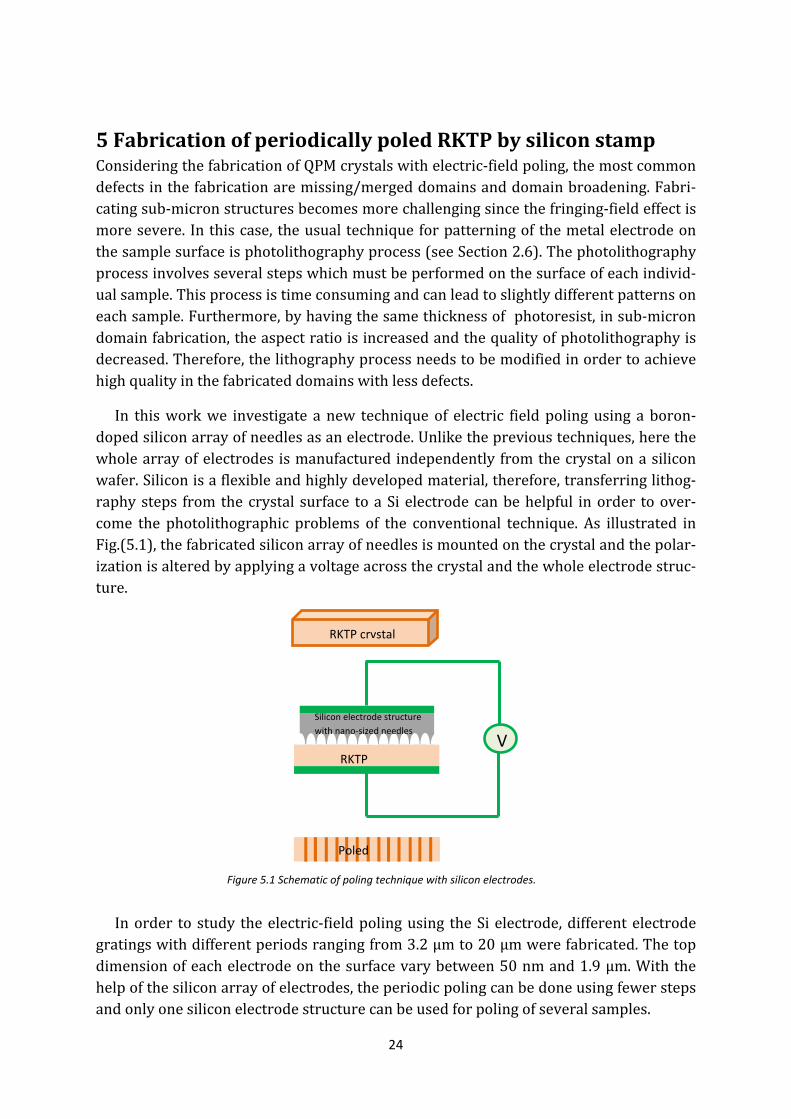
5FabricationofperiodicallypoledRKTPbysiliconstampConsideringthefabricationofQPMcrystalswithelectric‐fieldpoling,themostcommondefectsinthefabricationaremissing/mergeddomainsanddomainbroadening.Fabri‐catingsub‐micronstructuresbecomesmorechallengingsincethefringing‐fieldeffectismoresevere. Inthiscase, theusualtechniqueforpatterningofthemetalelectrodeonthesamplesurfaceisphotolithographyprocess(seeSection2.6).Thephotolithographyprocessinvolvesseveralstepswhichmustbeperformedonthesurfaceofeachindivid‐ualsample.Thisprocessistimeconsumingandcanleadtoslightlydifferentpatternsoneachsample.Furthermore,byhavingthesamethicknessofphotoresist,insub‐microndomainfabrication,theaspectratioisincreasedandthequalityofphotolithographyisdecreased.Therefore,thelithographyprocessneedstobemodifiedinordertoachievehighqualityinthefabricateddomainswithlessdefects.
In thisworkwe investigate anew techniqueof electric fieldpolingusing aboron‐dopedsiliconarrayofneedlesasanelectrode.Unliketheprevioustechniques,herethewholearrayofelectrodes ismanufacturedindependently fromthecrystalonasiliconwafer.Siliconisaflexibleandhighlydevelopedmaterial,therefore,transferringlithog‐raphysteps fromthecrystal surface toaSielectrodecanbehelpful inorder toover‐come the photolithographic problems of the conventional technique. As illustrated inFig.(5.1),thefabricatedsiliconarrayofneedlesismountedonthecrystalandthepolar‐izationisalteredbyapplyingavoltageacrossthecrystalandthewholeelectrodestruc‐ture.
Inorder to study theelectric‐fieldpolingusing theSielectrode,differentelectrode
gratingswithdifferentperiodsrangingfrom3.2μmto20μmwerefabricated.Thetopdimensionofeachelectrodeonthesurfacevarybetween50nmand1.9µm.Withthehelpofthesiliconarrayofelectrodes,theperiodicpolingcanbedoneusingfewerstepsandonlyonesiliconelectrodestructurecanbeusedforpolingofseveralsamples.
V
RKTP
RKTP crystal
Poled
Silicon electrode structure
with nano‐sized needles
Inthistyofthly‐pole
5.1Sam
ThemaRKTPwcrystalldirectiosamecbekept
5.2Po
Thepothehigshownotheratalmansaturatthecry
5.3Fa
Severalbestreduratiorameteforthecontrolidone,onds.S[4].Thethe nuc
chapter,pehecreatedddcrystalsi
mpleprep
aterialusedwaferwaslographic aonineachwconductivitytinthesam
olingsetup
olingsetupgh voltage.inFig.(5.2andtokeepnually. ThetedKClsoluystalandth
brication
lparametesults.Thepon, thepulsers. Inthefappliedvolled(duetotheelectriShortelectresiliconelecleation sta
eriodicpolidomainstruisevaluated
paration
d in thiswcut into saaxes, respewafer,eachy [20].Themeorderas
p
includedaThe samp),andwerpthemincoe crystal anutionwhichesiliconel
nofPPRKT
ers canbepressurebse shapeaframeoftholtage.Theothemanuicalpulsesric‐fieldpuectrodestrarted from
ingwiththucturesissd.
work isRb‐amplesofdectively. Sihcolumninerefore,dusintheiniti
aholderanle holder ceusedtofontact.Thend the silichgivesamectrode.
Figure
TP
adjusteddetweenthend themahiswork,apressurebualaligningwerechosulsesdecreructurewasm this face.
25
histechniqustudiedand
‐dopedpotdimensionince the conthex‐axisuring theclialwaferb
ndanelectrconsisted ofixtheelecesiliconelecon electromoreunifor
5.2 Poling cell
during theecrystalanagnitudeofallparametbetweenthgandmounsentobetrasethedosconnecteThe polar
ueisdiscusdtheoptica
tassium titas10 5onductivityswasexpecleaningprooxtomake
riccircuitwof two liqutrodestrucectrodewasodewere cmconnecti
.
polingprondtheelectf theapplieterswereshecrystalannting).Sincriangularwmainspreadtothecrization inv
ssed.Furthalperforma
anylphosp1mmalo
y mainly vactedtohavocedure, thefurtheran
whichwasuid electrodctureandtscenteredonnected tionoverth
cess inordtrode,theeedelectricsetatconstndmaskcoethepolinwithaduraadingbeyopolarfaceversionwa
hermore,thanceofper
phate (RKTong thea,aries alongvemoreorhesamplesnalysissimp
usedforade cellswhthecrystalontopofthto the circuhewholesu
der toachielectric‐fielfieldarestantvaluesouldnotbengprocessiationof5mondtheeleeofthecrysas executed
hequali‐riodical‐
TP).Thebandcg the y‐lessthes shouldpler.
applyinghich aretoeachhecrys‐uit by aurfaceof
ieve theldpulseuchpa‐sexcepteideallyisarap‐millisec‐ectrodesstalandd for 24
26
RKTPsamples.Twodifferentsiliconmasks,withaperiodicityofΛ=5µmandΛ=20µm,wereusedfortheperiodicpoling.
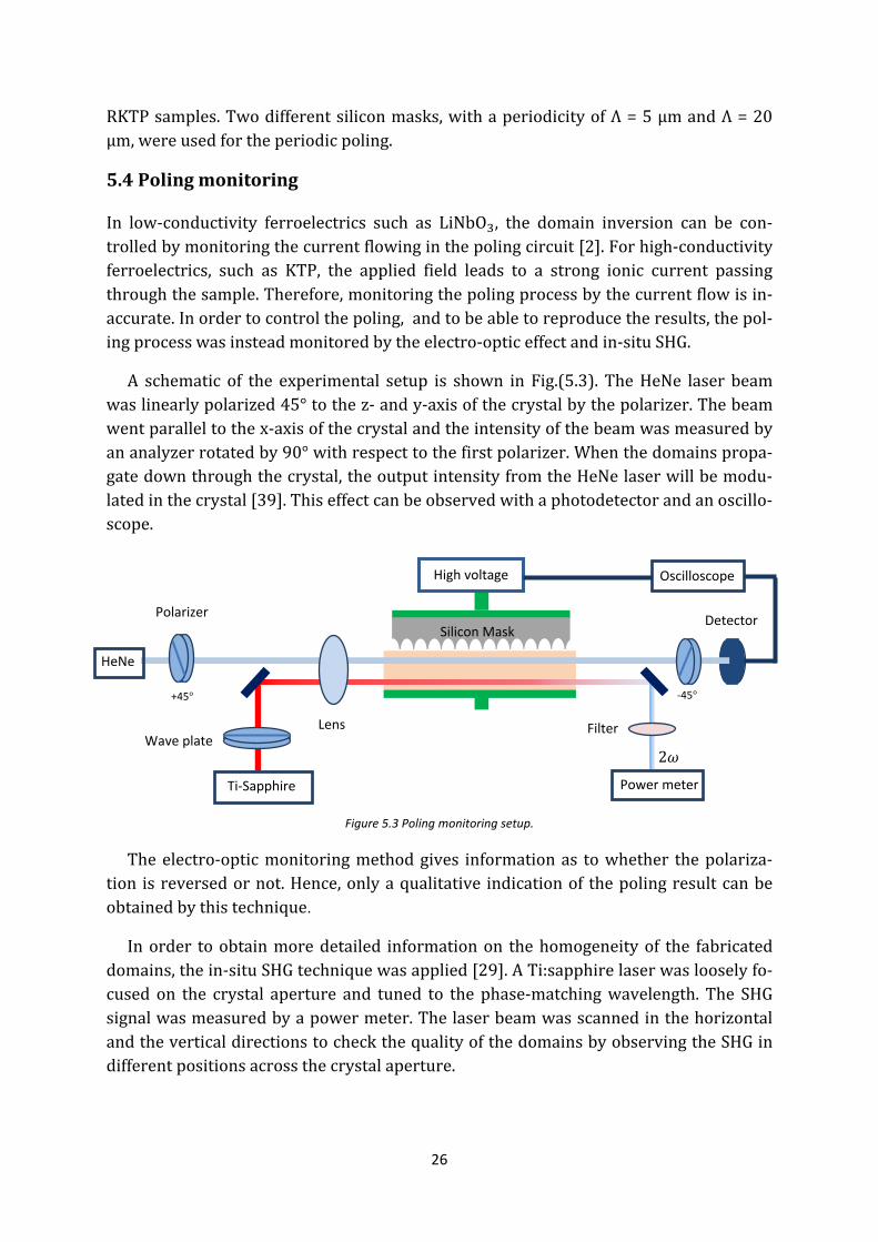
5.4Polingmonitoring
In low‐conductivity ferroelectrics such as LiNbO , the domain inversion can be con‐trolledbymonitoringthecurrentflowinginthepolingcircuit[2].Forhigh‐conductivityferroelectrics, such as KTP, the applied field leads to a strong ionic current passingthroughthesample.Therefore,monitoringthepolingprocessbythecurrentflowisin‐accurate.Inordertocontrolthepoling,andtobeabletoreproducetheresults,thepol‐ingprocesswasinsteadmonitoredbytheelectro‐opticeffectandin‐situSHG.
A schematic of the experimental setup is shown in Fig.(5.3). TheHeNe laser beamwaslinearlypolarized45°tothez‐andy‐axisofthecrystalbythepolarizer.Thebeamwentparalleltothex‐axisofthecrystalandtheintensityofthebeamwasmeasuredbyananalyzerrotatedby90°withrespecttothefirstpolarizer.Whenthedomainspropa‐gatedownthroughthecrystal,theoutputintensityfromtheHeNelaserwillbemodu‐latedinthecrystal[39].Thiseffectcanbeobservedwithaphotodetectorandanoscillo‐scope.
Figure 5.3 Poling monitoring setup.
Theelectro‐opticmonitoringmethodgives informationas towhether thepolariza‐tion isreversedornot.Hence,onlyaqualitative indicationof thepolingresultcanbeobtainedbythistechnique.
Inorder toobtainmoredetailed informationon thehomogeneityof the fabricateddomains,thein‐situSHGtechniquewasapplied[29].ATi:sapphirelaserwaslooselyfo‐cused on the crystal aperture and tuned to the phase‐matchingwavelength. The SHGsignalwasmeasuredbyapowermeter.ThelaserbeamwasscannedinthehorizontalandtheverticaldirectionstocheckthequalityofthedomainsbyobservingtheSHGindifferentpositionsacrossthecrystalaperture.
Silicon Mask
+45° ‐45°
High voltage
Detector
Oscilloscope
Ti‐Sapphire
HeNe
Polarizer
Lens Filter
Power meter
Wave plate 2

27
AsaCWTi:sapphire laser(SpectraPhysicsModel3900S,pumpedbya10WMilenniaX )hasemissionlinesbetween700nmand950nm,theQPMgratingperiodof5µmcanbeevaluatedbyusingthe1storderSHG,i.e.,λ 894nm.FortheperiodsofΛ=20µmthe5thorderSHGhastobeusedwitha fundamentalwavelengthofλ 842nm(ac‐cordingtoEquation2.14).
6Cha
6.1Sel
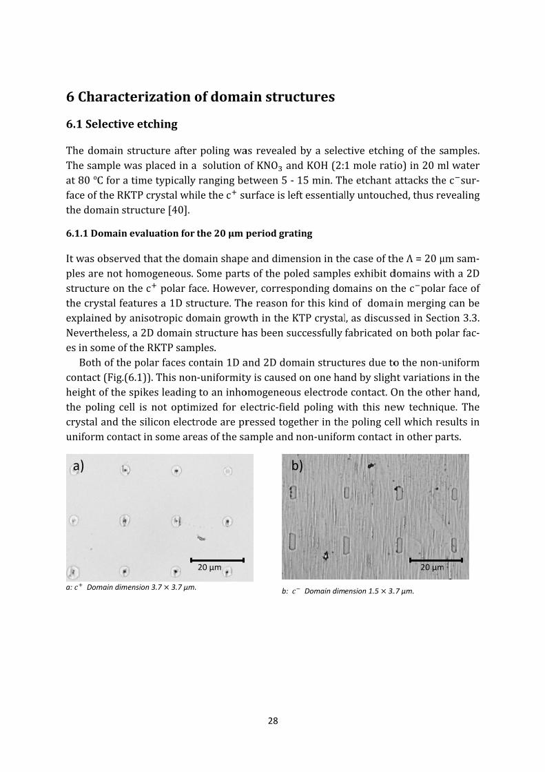
ThedoThesamat80faceofthedom
6.1.1Do
ItwasoplesarstructuthecryexplainNeverthesinsoBoth
contactheightthe polcrystaluniform
a: Dom
a)
aracteri
lectiveet
omainstrucmplewaspforatimetheRKTPcmainstruct
omaineval
observedthenothomoureonthecystalfeaturnedbyanisheless,a2DomeoftheRhofthepolt(Fig.(6.1))ofthespikling cell isandthesilmcontactin
main dimension
izationo
ching
ctureafterplacedinaetypicallycrystalwhiture[40].
luationfor
hatthedomogeneous.c polarfaesa1DstrsotropicdoDdomainsRKTPsamplarfacesco).Thisnonkesleadingnot optimliconelectrnsomeare
n 3.7 3.7 µm.
ofdoma
polingwasolutionorangingbeilethec su
the20µmp
mainshapeSomepartsce.Howeveructure.Thmaingrowstructurehples.ontain1Da‐uniformitytoaninho
mized for elrodearepreasofthesa
20 µm
28
ainstruc
as revealedofKNO anetween5‐urfaceisle
periodgrat
eanddimesofthepoer,corresphereasonfowthintheKhasbeensu
and2Ddomyiscausedomogeneoulectric‐fieldressedtogeampleand
b:
b
ctures
dbya selecndKOH(2:15min.Thftessential
ting
nsioninthledsamplepondingdoorthiskindKTPcrystaluccessfully
mainstructdononehauselectroded polingwetherinthenon‐unifor
Domain dim
b)
ctiveetchin1moleratiheetchantllyuntouch
ecaseofthesexhibitdmainsontdofdomal,asdiscusfabricated
turesduetondbyslighecontact.Owith this neepolingcermcontact
ension 1.5 3.
ngof thesio)in20mattacksthehed,thusre
heΛ=20μdomainswithec polarainmergingsedinSectonbothpo
othenon‐uhtvariationOntheotheew techniqellwhichreinotherpa
.7 µm.
20 µm
amples.mlwaterec sur‐evealing
μmsam‐itha2Drfaceofgcanbetion3.3.olarfac‐
uniformnsintheerhand,que. Theesultsinarts.
m
c: Dom
e: Dom
µm in betw
Figure 6.1
kV/mm w
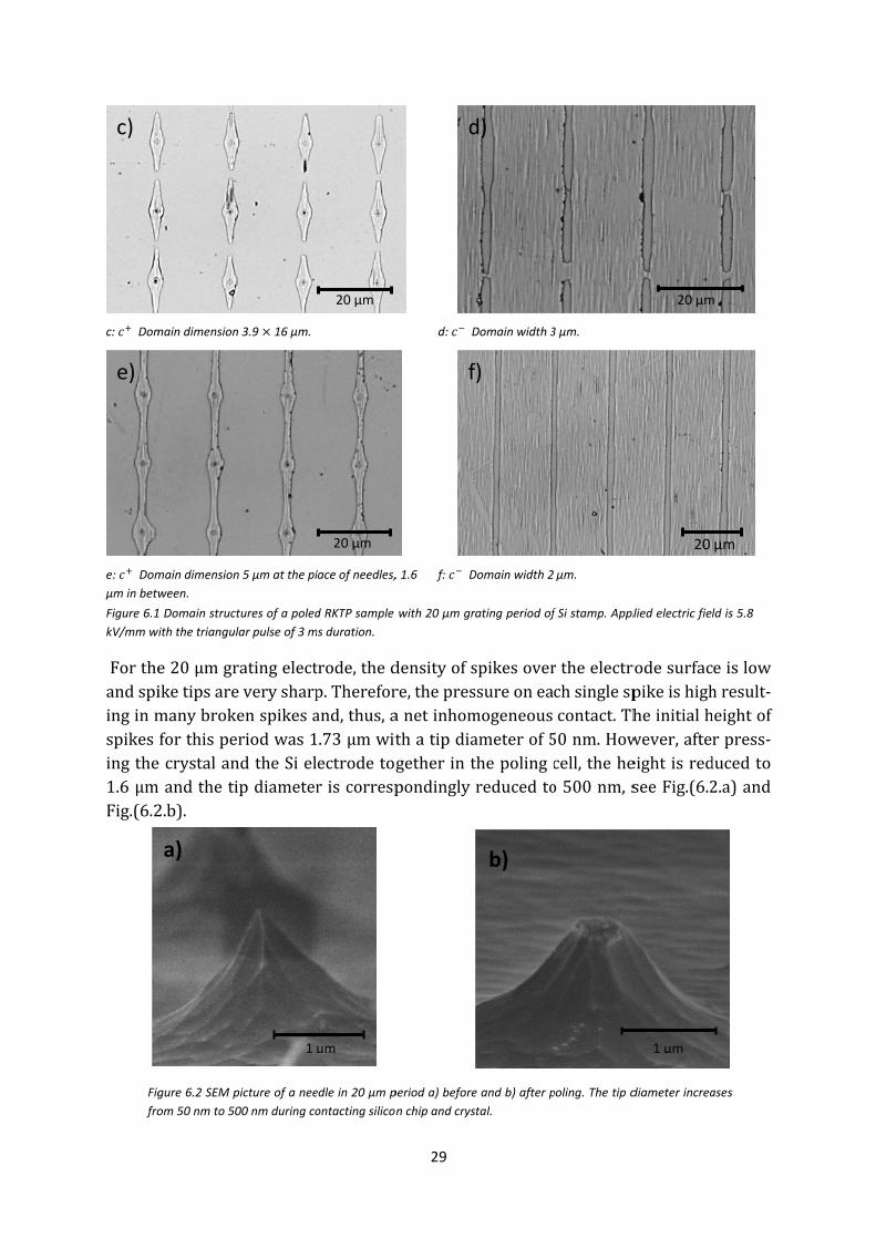
Fortheandspiinginmspikesingthe1.6µmFig.(6.2
Fig
fro
c)
e)
main dimension
main dimension
ween.
1 Domain struct
ith the triangul
e20µmgriketipsaremanybrokeforthispeecrystalanmandtheti2.b).
gure 6.2 SEM p
om 50 nm to 50
a)
n 3.9 16 µm.
n 5 µm at the pl
tures of a poled
lar pulse of 3 m
ratingelecteverysharpenspikesariodwas1ndtheSielipdiameter
picture of a nee
00 nm during co
1
lace of needles,
d RKTP sample
ms duration.
trode,thedp.Thereforand,thus,a1.73µmwitectrodetogriscorresp
edle in 20 µm p
ontacting silicon
µm
20 µm
20 µm
29
d: D
, 1.6
f: D
with 20 µm gr
densityofsre,thepresanetinhomthatipdiagetherintpondingly
period a) before
n chip and crys
d
f
Domain width 3
Domain width 2
rating period of
spikesoverssureoneamogeneousameterof5thepolingcreducedto
e and b) after p
tal.
b)
d)
f)
3 µm.
µm.
f Si stamp. Appl
rtheelectrchsinglespcontact.Th50nm.Howcell,theheo500nm,s
poling. The tip d
lied electric fiel
rodesurfacpikeishighheinitialhwever,afteeightisredseeFig.(6.2
diameter increa
1 µm
20 µm
20
ld is 5.8
eislowhresult‐heightofrpress‐ducedto2.a)and
ases
m
µm
Besidesbrokencaused
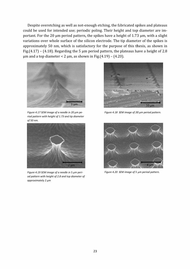
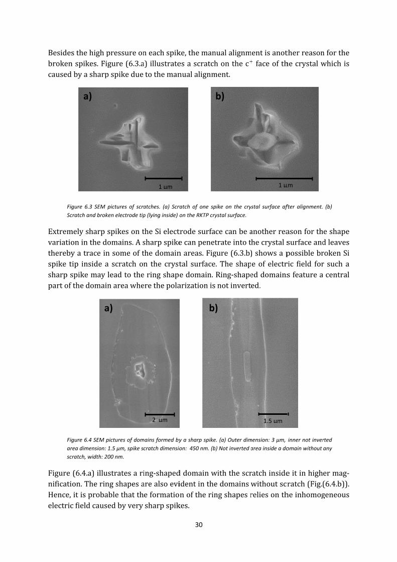
Fig
Sc
Extremvariatiotherebyspike tsharpspartof
Fig
ar
sc
FigurenificatiHence,electric
sthehighpnspikes.Figbyasharp
gure 6.3 SEM p
cratch and brok
melysharpsoninthedoyatraceintip insideaspikemaythedomain
gure 6.4 SEM p
rea dimension:
cratch, width: 20
(6.4.a)illuon.Therinitisprobacfieldcaus
a
a)
pressureongure(6.3.apspikedue
pictures of scra
ken electrode tip
spikesontomains.Asnsomeofta scratcholeadtothenareawhe
pictures of dom
1.5 µm, spike s
00 nm.
stratesaringshapesaablethatthedbyvery
a)
neachspika)illustratetotheman
atches. (a) Scra
p (lying inside) o
theSielectsharpspikethedomainn the crysteringshaperethepola
mains formed by
cratch dimensio
ing‐shapedarealsoevieformatiosharpspik
1 µm
2 µm
30
ke,themanesascratchnualalignm
ratch of one sp
on the RKTP cry
trodesurfaecanpenetnareas.Figtal surfaceedomain.arizationis
y a sharp spike
on: 450 nm. (b
ddomainwidentinthenoftherinkes.
b)
nualalignmhonthecment.
pike on the cry
ystal surface.
cecanbeatrateintotgure(6.3.b). The shapRing‐shapenotinvert
e. (a) Outer dim
b) Not inverted a
withthescredomainswngshapesr
)
b)
mentisanotfaceofth
stal surface af
anotherreahecrystals)showsapeof electreddomainsed.
mension: 3 µm,
area inside a do
ratchinsidewithoutscrreliesonth
1 µ
1.5 µm
therreasonhecrystalw
fter alignment.
asonforthsurfaceandpossiblebrric field forsfeaturea
inner not inver
omain without
eitinhighratch(Fig.(heinhomog
µm
nforthewhichis
(b)
eshapedleavesrokenSir such acentral
rted
any
ermag‐(6.4.b)).geneous
31
Figure (6.1)shows thedomainstructuresofoneparticularRKTPsample fordifferentpartsof thecrystal.Thereare2Ddomainstructuresaswellaselongated2Ddomainsand1Ddomainson thec polar face(Fig.(6.1.a), (6.1.c), (6.1.e)).Theircorrespondingdomainsonthec faceareshownontherighthandside(Fig.(6.1.b),(6.1.d),(6.1.f)).Inmostofthedomainsonthec face,ring‐shapedandspikescratchescanbeobserved.
Sincethespiketipdiameterisincreasedafterthesamplemounting,thefabricateddo‐main dimensions are larger thanwhatwas anticipated. Due to the quasi‐one dimen‐sionalstructureoftheRKTP,2Ddomainstendtomergetogetherintheb‐directionandforma1Ddomainstructure.Therefore,insamplescontaining2Ddomainstructures,thefabricateddomainsarelargeralongtheb‐axis(~3.5‐4.2µm)andnarroweralongthea‐axis(~2.4‐3.8µm).Theircorrespondingdomainsonthec polarfacefollowsthesamecriteria.Insampleswith1Ddomainsonthec polarface,thewidthofthedomainsinthea‐directionislargeratthelocationofthespikecontact(~4.1μ )andnarrowerinbetween (~1.6 µm). The information regarding thedomains dimensions in bothpolarfacesarelistedinTable(6.1).Thereasonforthisisthehighvalueofthefringingfieldaroundthespiketipandalsothehardcontactoftheelectrodeandthecrystalsurface.Thecorresponding1Ddomainsonthec polarfacearehomogenousandhaveawidthof1.9µm.
Domaintype 2D Elongated2D 1D
Dimensioninc 3.7µm 3.7µm 3.8µm 16.5µm 1.6&4.1µm
Dimensioninc 1.5µm 3.7µm 2.9µm 1.9µm
Table 6.1 Domain shape and dimension in Λ = 20 µm grating
6.1.2Domainevaluationfor5µmperiodgratingSixRKTPsampleswerepoledwitha5µmgratingelectrode.Gratingpatternsof5µmperiods are successfully reproduced on the polar faces of the crystal by applying anelectricfieldof5.4kV mm⁄ withatriangularpulseof5msduration.
Fabricateddomainstructureswitha5µmperiodsiliconelectrodeismoreuniformacrossthecrystalsurface.Uniformdomainstructurescomefromthefactthatthecon‐tactareaofthecrystalsurfaceandtheelectrodeisnowmorehomogenousthanintheΛ=20μmcase.Severalparametersleadtotheuniformcontact.First,alltheplateausonthesiliconarrayofelectrodeshavethesameheight.Second, topareasoftheplateausare perfectly flat because they have the initial surface of the siliconwafer. Third, thedensityof theplateaus ishighoverthewholesurfaceandthisresults ina total lowerpressureoneachindividualneedleelectrode.Therefore,betterdomaingratingqualityistobeexpectedfortheRKTPsamplespoledwithΛ=5μmSielectrodes.However,theproblemof themanualalignmentand thepressingof thesiliconarrayandcrystal to‐getherstillaffectsthepolingprocess.
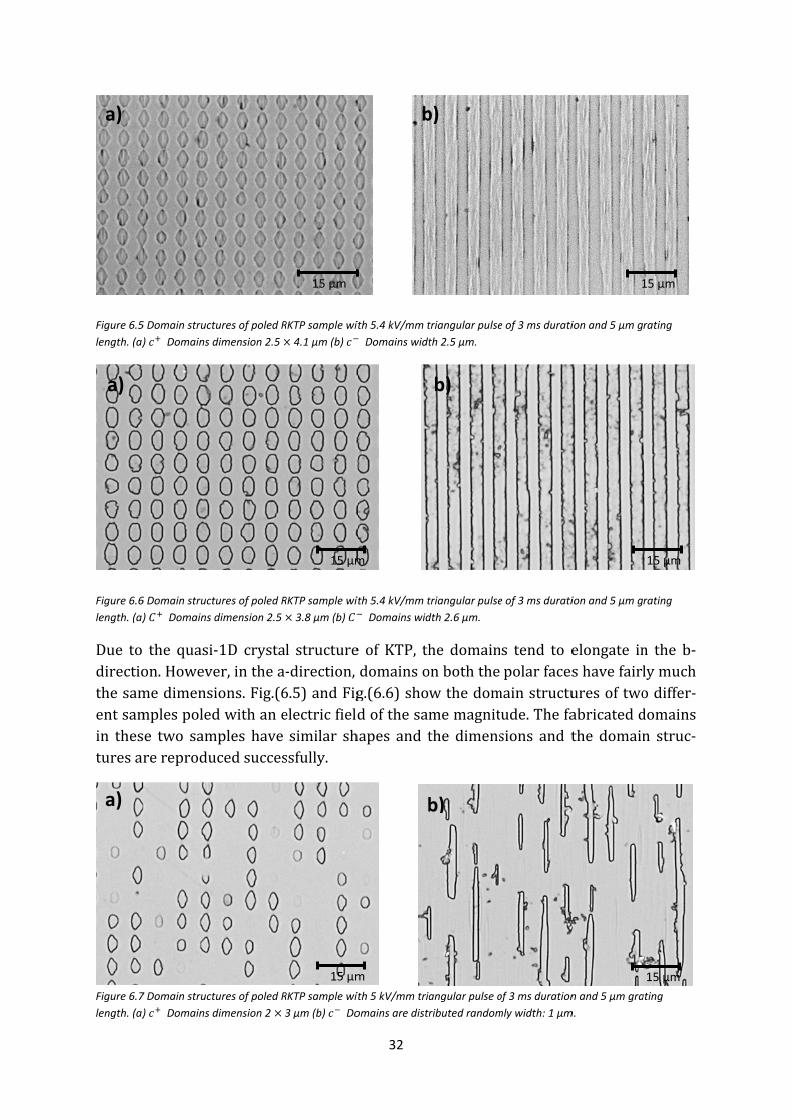
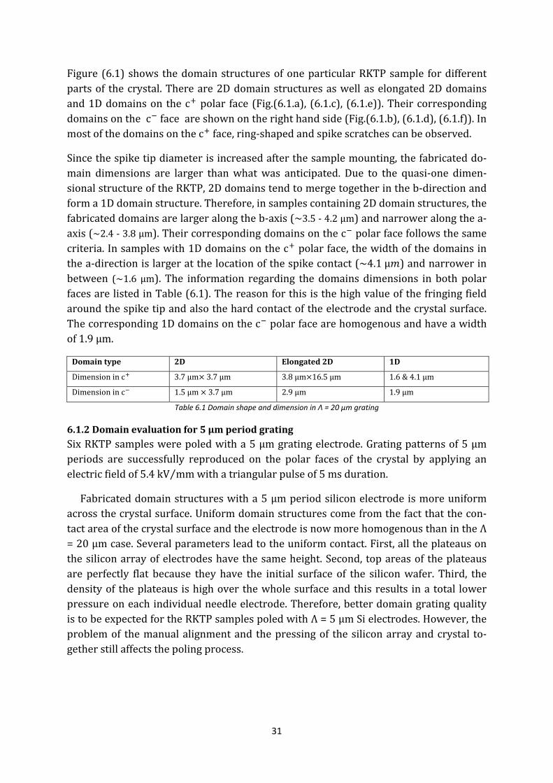
Figure 6.5
length. (a)
Figure 6.6
length. (a)
Due todirectiothesamentsamin thesturesa
Figure 6.7
length. (a)
a)
a)
a)
5 Domain struct
) Domains d
6 Domain struct
) Domains d
the quasi‐on.Howevemedimensimplespoledse two samrereprodu
7 Domain struct
) Domains d
tures of poled R
dimension 2.5
tures of poled R
dimension 2.5
‐1D crystaer,inthea‐ions.Fig.(6dwithanemples haveucedsucces
tures of poled R
dimension 2 3
RKTP sample wi
4.1 µm (b)
RKTP sample wi
3.8 µm (b)
l structure‐direction,6.5)andFigelectricfieldsimilar shssfully.
RKTP sample wi
3 µm (b) Do
15 µm
15 µm
15 µm
32
ith 5.4 kV/mm t
Domains widt
ith 5.4 kV/mm t
Domains wid
e of KTP, thdomainsog.(6.6)shodofthesamhapes and t
ith 5 kV/mm tria
omains are distr
b
b
m
m
triangular pulse
th 2.5 µm.
triangular pulse
dth 2.6 µm.
he domainonboththewthedommemagnitthe dimens
angular pulse o
ributed random
b)
b)
b)
e of 3 ms durati
e of 3 ms durati
s tend to epolarfaces
mainstructuude.Thefasions and t
of 3 ms duration
mly width: 1 µm
ion and 5 µm g
ion and 5 µm g
elongate inshavefairluresoftwoabricateddthe domain
n and 5 µm gra
m.
1
rating
rating
n the b‐lymuchodiffer‐domainsn struc‐
ating
15 µm
15 µm
15 µm
33
On the other hand, inhomogeneous pressure, lower applied electric field, and lack ofgoodalignmentresultinmanymissingdomainsasisshowninFig.(6.7).
6.2Opticalcharacterization
Thesiliconspikesareverysharpforthe20µmperiodelectrodes.Thisresultsinanon‐optimal duty cycle of the fabricated domain structures. 5th order SHG process in thedomainstructureswithnon‐optimaldutycycleresultsinaverylowSHsignal.However,inthecaseofthe5µmgrating,sincethedutycycleinthiscaseisclosetotheidealcaseof50%,the1storderSHGprocesswithameasurablesignalpower,isobserved.Inordertoevaluatethequalityof the fabricatedgratings in theRKTPcrystals, theopticalper‐formanceoftwoofthesampleswiththeΛ=5µmgratingwereinvestigated.Thegener‐ated SH signal which was created in this experiment is close to c polar face, corre‐spondsto[1,0]reciprocallatticevector(RLV).ThisRLVisequivalentto1Dgrating.
6.2.1Conversionefficiency
Oneway to check thepolingquality is to observe the SH conversion efficiencyof thepoledcrystal.ForaGaussianbeam,theconversionefficiency isgivenbythefollowingexpression[41]:
η Lh B, ξ . (6.1)
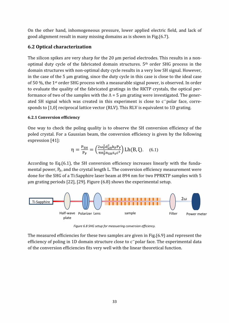
According to Eq.(6.1), the SH conversion efficiency increases linearlywith the funda‐mentalpower,P ,andthecrystallengthL.TheconversionefficiencymeasurementweredonefortheSHGofaTi:Sapphirelaserbeamat894nmfortwoPPRKTPsampleswith5µmgratingperiods[22],[29].Figure(6.8)showstheexperimentalsetup.
Figure 6.8 SHG setup for measuering conversion efficiency.
ThemeasuredefficienciesforthesetwosamplesaregiveninFig.(6.9)andrepresenttheefficiencyofpolingin1Ddomainstructureclosetoc polarface.Theexperimentaldataoftheconversionefficienciesfitsverywellwiththelineartheoreticalfunction.
Power meter
Ti‐Sapphire
Polarizer Lens Filter
2
Half‐wave plate
sample
34
0 100 200 300 400-0,05
0,00
0,05
0,10
0,15
0,20
0,25
0,30 efficiency (sample #1) efficiency (sample #2)
effic
ien
cy(%
)
PF(mW)
0 50 100 150 200 250 300 350 400 450
0
200
400
600
800
1000
1200 SH power (sample #1) SH power (sample #2)
PS
H(µ
W)
PF(mW)
Figure 6.9 The SHG conversion efficiency as a function of fundamental power for 2 samples with 5 µm grat‐
ing period. Circles and squares are measured data and red lines are linear fis, respectively.
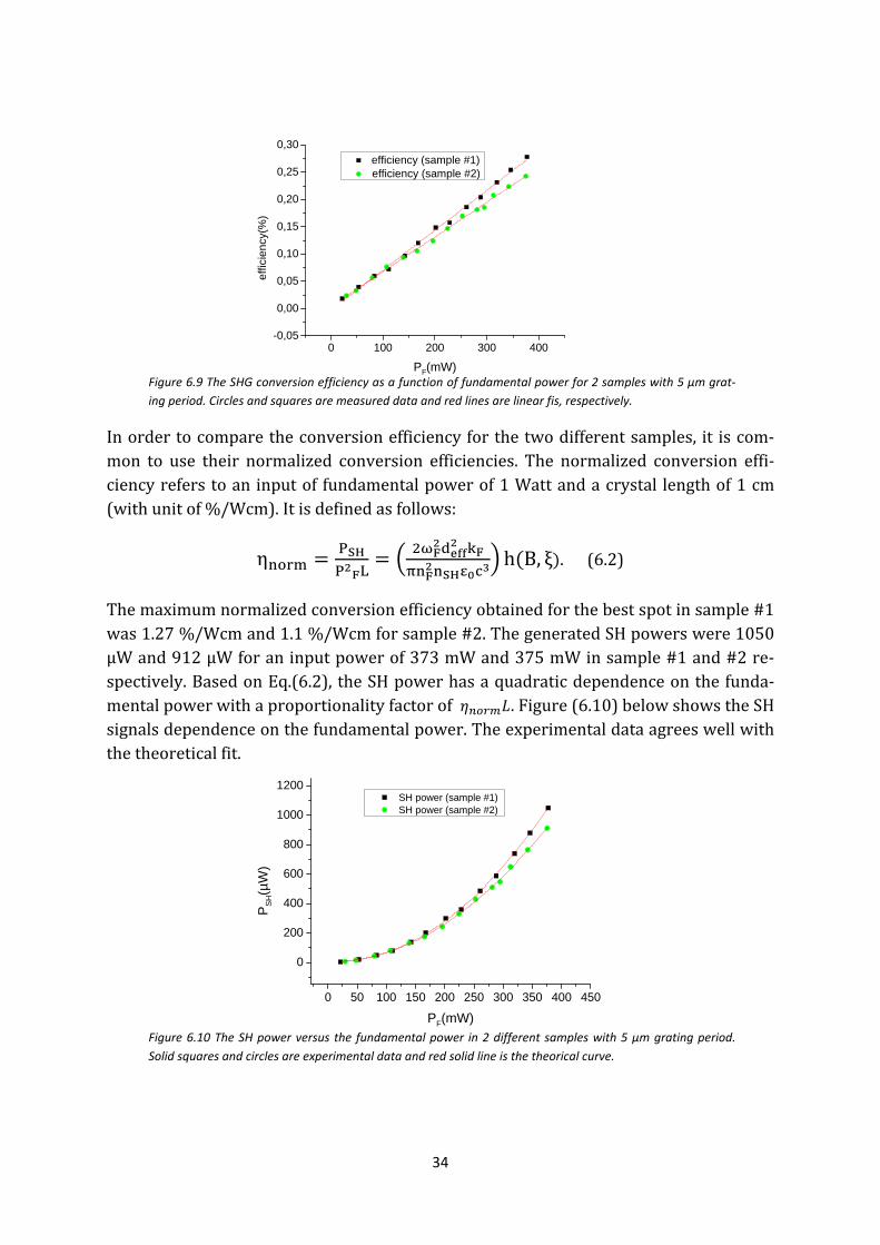
Inordertocomparetheconversionefficiencyforthetwodifferentsamples, it iscom‐mon to use their normalized conversion efficiencies. The normalized conversion effi‐ciencyreferstoaninputof fundamentalpowerof1Wattandacrystal lengthof1cm(withunitof%/Wcm).Itisdefinedasfollows:
η h B, ξ .(6.2)
Themaximumnormalizedconversionefficiencyobtainedforthebestspotinsample#1was1.27%/Wcmand1.1%/Wcmforsample#2.ThegeneratedSHpowerswere1050µWand912µWforaninputpowerof373mWand375mWinsample#1and#2re‐spectively.BasedonEq.(6.2),theSHpowerhasaquadraticdependenceonthefunda‐mentalpowerwithaproportionalityfactorof .Figure(6.10)belowshowstheSHsignalsdependenceonthefundamentalpower.Theexperimentaldataagreeswellwiththetheoreticalfit.
Figure 6.10 The SH power versus the fundamental power in 2 different samples with 5 µm grating period.
Solid squares and circles are experimental data and red solid line is the theorical curve.
35
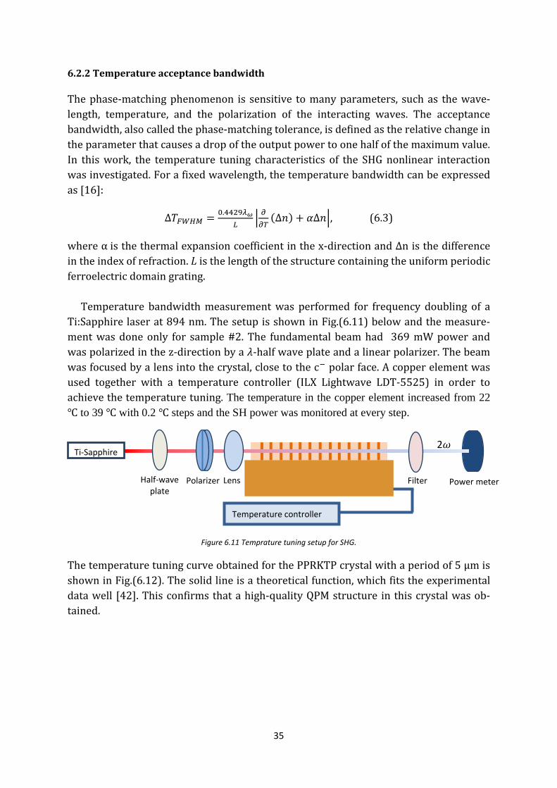
6.2.2Temperatureacceptancebandwidth
Thephase‐matchingphenomenon is sensitive tomanyparameters, suchas thewave‐length, temperature, and the polarization of the interacting waves. The acceptancebandwidth,alsocalledthephase‐matchingtolerance,isdefinedastherelativechangeintheparameterthatcausesadropoftheoutputpowertoonehalfofthemaximumvalue.In thiswork, the temperature tuning characteristics of the SHG nonlinear interactionwasinvestigated.Forafixedwavelength,thetemperaturebandwidthcanbeexpressedas[16]:
∆ . Δ Δ ,(6.3)
whereαisthethermalexpansioncoefficientinthex‐directionandΔnisthedifferenceintheindexofrefraction.Listhelengthofthestructurecontainingtheuniformperiodicferroelectricdomaingrating.Temperature bandwidthmeasurementwas performed for frequency doubling of a
Ti:Sapphirelaserat894nm.ThesetupisshowninFig.(6.11)belowandthemeasure‐mentwasdoneonly for sample#2.The fundamentalbeamhad 369mWpower andwaspolarizedinthez‐directionbya ‐halfwaveplateandalinearpolarizer.Thebeamwasfocusedbyalensintothecrystal,closetothec polarface.Acopperelementwasused together with a temperature controller (ILX Lightwave LDT‐5525) in order toachievethetemperaturetuning. The temperature in the copper element increased from 22
to 39 with 0.2 steps and the SH power was monitored at every step.
Figure 6.11 Temprature tuning setup for SHG.
ThetemperaturetuningcurveobtainedforthePPRKTPcrystalwithaperiodof5µmisshowninFig.(6.12).Thesolidlineisatheoreticalfunction,whichfitstheexperimentaldatawell [42].Thisconfirmsthatahigh‐qualityQPMstructure inthiscrystalwasob‐tained.
Power meter
Ti‐Sapphire
Polarizer Lens Filter
2
Half‐wave plate
Temperature controller
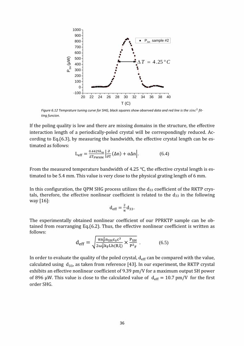
36
20 22 24 26 28 30 32 34 36 38 40-100
0
100
200
300
400
500
600
700
800
900
1000
PSH sample #2
PS
H (µ
W)
T (C)
CT 25.4
Figure 6.12 Temprature tuning curve for SHG, black squares show observed data and red line is the fit‐
ting funcion.
Ifthepolingqualityislowandtherearemissingdomainsinthestructure,theeffectiveinteraction lengthof aperiodically‐poled crystalwill be correspondingly reduced.Ac‐cordingtoEq.(6.3),bymeasuringthebandwidth,theeffectivecrystallengthcanbees‐timatedasfollows:
L .
∆Δn αΔn . (6.4)
Fromthemeasuredtemperaturebandwidthof4.25 ,theeffectivecrystallengthises‐timatedtobe5.4mm.Thisvalueisveryclosetothephysicalgratinglengthof6mm.Inthisconfiguration,theQPMSHGprocessutilizesthed33coefficientoftheRKTPcrys‐tals, therefore, the effectivenonlinear coefficient is related to thed33 in the followingway[16]:
d d .
The experimentally obtained nonlinear coefficient of our PPRKTP sample can be ob‐tainedfromrearrangingEq.(6.2).Thus,theeffectivenonlinearcoefficient iswrittenasfollows:
d,
. (6.5)
Inordertoevaluatethequalityofthepoledcrystal,d canbecomparedwiththevalue,calculatedusingd ,astakenfromreference[43].Inourexperiment,theRKTPcrystalexhibitsaneffectivenonlinearcoefficientof9.39pm/VforamaximumoutputSHpowerof896µW.Thisvalueisclosetothecalculatedvalueofd 10.7pm/VforthefirstorderSHG.
37
6.2.3Domainmergingpointestimation
Thefabricateddomainswiththe2Darrayofsiliconelectrodeinthe5µmperiodsaretwo‐dimensional on the c faceof the crystal (where the electrode is in contact) andone‐dimensionalon thec polar face.Therefore,2Ddomainstructuresmergedalongtheb‐axisduringthepropagationandbecame1Donthenon‐contactfaceofthecrystal.Inordertofindtheexactpositionofthedomainmergingalongthepolardirectioninthecrystal,anSHGexperimentwasconducted inoneof thePPRKTPcrystals.Theexperi‐mentalsetupisillustratedinFig.(6.8)andwasperformedusingtheCWTi:Sapphirela‐serlasingatawavelengthof894nm.BasedontheconceptwhichisexplainedinSection2.7, the generated SH signal with this structure includes side peakswhich representmorethanonepossiblek‐vectorina2DQPMstructureclosetothec face.WhentheTi:Sapphire laser beamwas scanned over the crystal thickness, the side peaks disap‐pearedassoonas the2Dstructurebecame1D.The2Ddomainstructuremergedandbecamea1Ddittoatadistanceof0.21mmfromthec face.

38
7ConclusionsIn thiswork,anewmethod for fabricationofperiodically‐poledcrystals ispresented.Thismethod is based on using an array of silicon spikes as an electrode for contactwhenperforming electric‐fieldpolingofRKTP.Theprocess for fabricatingthesiliconspikes is designed and subsequently optimized for different electrode shapes andformes.Thefinalmethodisflexible,repeatable,andeasytomodifyforproducingnewtypes of electrodeswith different sizes and geometries. The periodicity of the spikesranges from3.2 µmup to 20 µm. The process of producing spike array electrodes isoverviewedindetail. The constructed Si spike arrays are used as a 2D contact electrode for poling the
RKTPwithtwodifferentperiodicitiesof20µmand5µm,respectively.Eachindividualsiliconelectrodeonthefinalsiliconarrayofelectrodeshasaconicalshapeinthe20µmperiodcaseandaplateaushapeinthe5µmperiodcase.Theconical‐shapedelectrodeshavevery sharp spike tips resulting in apoorly controlledpressure in thepoling cellemployed. In the 20 µm period, the fabricated domains show pattern broadening.Nonetheless, the broadening can be reduced bymaskmodification and by improvingthe poling cell. The plateau‐shaped electrodes produce domain structures which aresimilartothefabricateddomainsusingconventionaltechnique.Thedomainbroadeningfor the 5 µm period case has the same scale as that of the broadening with metal‐depositedelectrodes.However, it canbe reducedby improving thepolingcell andbycontrolling the pressure between theRKTP crystal and the silicon electrode. The do‐mainbroadeningisalsoaffectedbytheelectrodegeometryandcanbeadjustedbymod‐ifying the geometryof theplateau fordifferentperiods.Moreover, the fabricateddo‐mainsforthisperiodarereproducedbyapplyingthesameparametersfortwodifferentsamples.Tothebestofourknowledge,thisisthefirsttimethistechniquehasbeenusedforfabricatingperiodicallypoledRKTP(PPRKTP). Theduty cycleof the fabricateddomains for the5µmperiods is close to the ideal
caseof50%.Therefore,theopticalperformanceofthePPRKTPcrystalswiththisperi‐odwas further evaluated.Two samplespoledwith5µmperiodareused to generatesecond‐harmonic (SH) signals and to investigate the conversion efficiency of the SHprocess for fabricatingQPMdevices. Thenormalized conversionefficiencies for thesetwo samples are higher than 1%/Wcm and, thus, this indicates good optical perfor‐mance. The evaluated effective grating length from the measured temperature ac‐ceptancebandwidth is5.4mm,which is close to thephysicalgrating lengthof6mm.Thus, the fabricateddomainsareuniformlystructureddemonstratingthehigh‐qualitypolingobtainedwiththistechnique.
39
7.1Furtherdevelopments
Thereisavarietyofinterestingfutureexperimentsthatcanbedonebasedonthiswork.Theycanbedivided into twomaincategories:1)modificationof thesiliconelectrodestructureand2)moredetailedinvestigationofthepolingprocess.
Itwasobservedthatbyusingsharpspikes for thepoling, resulted innon‐uniformcontactandnon‐homogenousring‐shapeddomainstructures.Therefore,inthecaseofsilicon electrode modification, first, it is beneficial to polish the spike electrode andthereby reduce the sharpness. Second, the spikes and the plateaus can be fabricatedwithalargerheightbyintroducingtheBoschprocess.Anarrayofsiliconspikesorplat‐eauswithlargeheightcanbepartiallycoveredwithalayerofphotoresistresultinginabetterisolationduringthepolingprocess.Third,inordertocontrolthedomainbroad‐ening,thegeometryofthesiliconspikeandplateauelectrodescanbemodified.Reduc‐ing theelectrodedimension in theb‐directioncouldresult in lessdomainbroadeningleadingtoacomplete2Ddomainstructureonboththepolarfacesofthecrystal.Forth,theelectrodematerialcanbechangedtoanalyzetheinfluenceofdifferentmaterialsonpoling.Thep‐type siliconelectrode canbe replacedbyann‐type siliconormetalizedpolymerspikes.Thefabricationofpolymerspikesisflexibleandwelldeveloped.There‐fore, a metalized polymer array of spikes can serve as a good alternative electrodechoicetothesiliconspikes.Furthermore,modifiationoftheelectrodestructurecanbedoneinordertoinvestigatethe1DperiodicpolingofKTP.Inordertoaccessthistech‐niqueforfabricatingdomainsinthenano‐scale,siliconelectrodespecificationsneedtobemodified.
Regardingthepolingprocessitself,thefollowingaspetscanbeimprovedupon.Thepolingcellshouldbeupgradedsoastoprovideabetterpressureandalignmentcontrol.Thepolingparameterssuchasthepulseshape,pulsedurationandthenumberofpulsescanbeoptimized.Thus,periodically‐poledcrystalswithhigherqualitycanbeobtained.
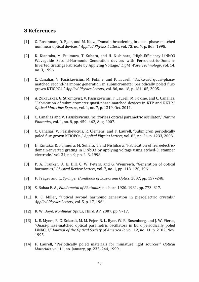
40
8References
[1] G.Rosenman,D.Eger,andM.Katz,“Domainbroadeninginquasi‐phase‐matchednonlinearopticaldevices,”AppliedPhysicsLetters,vol.73,no.7,p.865,1998.
[2] K. Kiantaka, M. Fujimura, T. Suhara, and H. Nishihara, “High‐Efficiency LiNbO3Waveguide Second‐Harmonic Generation devices with Ferroelectric‐Domain‐InvertedGratingsFabricatebyApplyingVoltage,”LightWaveTechnology,vol.14,no.3,1996.
[3] C. Canalias, V. Pasiskevicius, M. Fokine, and F. Laurell, “Backward quasi‐phase‐matchedsecond‐harmonicgeneration in submicrometerperiodicallypoled flux‐grownKTiOPO4,”AppliedPhysicsLetters,vol.86,no.18,p.181105,2005.
[4] A.Zukauskas,G.Strömqvist,V.Pasiskevicius,F.Laurell,M.Fokine,andC.Canalias,“Fabricationof submicrometerquasi‐phase‐matcheddevices inKTPandRKTP,”OpticalMaterialsExpress,vol.1,no.7,p.1319,Oct.2011.
[5] C.CanaliasandV.Pasiskevicius,“Mirrorlessopticalparametricoscillator,”NaturePhotonics,vol.1,no.8,pp.459–462,Aug.2007.
[6] C.Canalias,V.Pasiskevicius,R.Clemens,andF.Laurell, “Submicronperiodicallypoledflux‐grownKTiOPO4,”AppliedPhysicsLetters,vol.82,no.24,p.4233,2003.
[7] H.Kintaka,K,Fujimura,M,Suhara,TandNishihara,“Fabricationofferroelectric‐domain‐invertedgrating inLiNbO3byapplyingvoltageusingetched‐Sistamperelectrode,”vol.34,no.9,pp.2–3,1998.
[8] P. A. Franken, A. E. Hill, C.W. Peters, and G.Weinreich, “Generation of opticalharmonics,”PhysicalReviewLetters,vol.7,no.1,pp.118–120,1961.
[9] F.Trägerand...,SpringerHandbookofLasersandOptics.2007,pp.157–248.
[10] S.BahaaE.A.,FundametalofPhotonics,no.born1920.1981,pp.773–817.
[11] R. C. Miller, “Optical second harmonic generation in piezoelectric crystals,”AppliedPhysicsLetters,vol.5,p.17,1964.
[12] R.W.Boyd,NonlinearOptics,Third.AP,2007,pp.9–17.
[13] L.E.Myers,R.C.Eckardt,M.M.Fejer,R.L.Byer,W.R.Bosenberg,andJ.W.Pierce,“Quasi‐phase‐matched optical parametric oscillators in bulk periodically poledLiNbO_3,”JournaloftheOpticalSocietyofAmericaB,vol.12,no.11,p.2102,Nov.1995.
[14] F. Laurell, “Periodically poled materials for miniature light sources,” OpticalMaterials,vol.11,no.January,pp.235–244,1999.
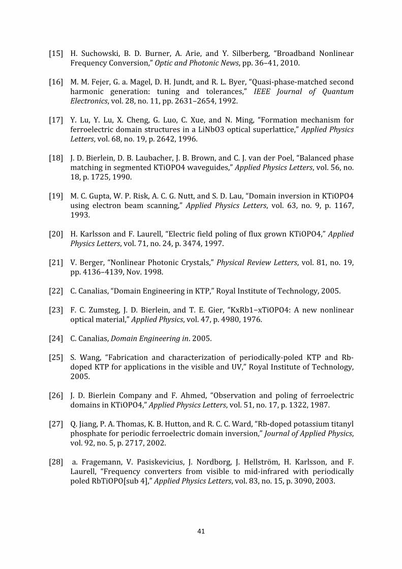
41
[15] H. Suchowski, B. D. Burner, A. Arie, and Y. Silberberg, “Broadband NonlinearFrequencyConversion,”OpticandPhotonicNews,pp.36–41,2010.
[16] M.M.Fejer,G.a.Magel,D.H.Jundt,andR.L.Byer,“Quasi‐phase‐matchedsecondharmonic generation: tuning and tolerances,” IEEE Journal of QuantumElectronics,vol.28,no.11,pp.2631–2654,1992.
[17] Y. Lu, Y. Lu, X. Cheng, G. Luo, C. Xue, and N. Ming, “Formation mechanism forferroelectricdomainstructuresinaLiNbO3opticalsuperlattice,”AppliedPhysicsLetters,vol.68,no.19,p.2642,1996.
[18] J.D.Bierlein,D.B.Laubacher,J.B.Brown,andC.J.vanderPoel,“BalancedphasematchinginsegmentedKTiOPO4waveguides,”AppliedPhysicsLetters,vol.56,no.18,p.1725,1990.
[19] M.C.Gupta,W.P.Risk,A.C.G.Nutt,andS.D.Lau,“DomaininversioninKTiOPO4using electron beam scanning,” Applied Physics Letters, vol. 63, no. 9, p. 1167,1993.
[20] H.KarlssonandF.Laurell,“ElectricfieldpolingoffluxgrownKTiOPO4,”AppliedPhysicsLetters,vol.71,no.24,p.3474,1997.
[21] V.Berger, “NonlinearPhotonicCrystals,”PhysicalReviewLetters, vol.81,no.19,pp.4136–4139,Nov.1998.
[22] C.Canalias,“DomainEngineeringinKTP,”RoyalInstituteofTechnology,2005.
[23] F. C. Zumsteg, J. D. Bierlein, and T. E. Gier, “KxRb1−xTiOPO4: A new nonlinearopticalmaterial,”AppliedPhysics,vol.47,p.4980,1976.
[24] C.Canalias,DomainEngineeringin.2005.
[25] S. Wang, “Fabrication and characterization of periodically‐poled KTP and Rb‐dopedKTPforapplicationsinthevisibleandUV,”RoyalInstituteofTechnology,2005.
[26] J. D. Bierlein Company and F. Ahmed, “Observation and poling of ferroelectricdomainsinKTiOPO4,”AppliedPhysicsLetters,vol.51,no.17,p.1322,1987.
[27] Q.Jiang,P.A.Thomas,K.B.Hutton,andR.C.C.Ward,“Rb‐dopedpotassiumtitanylphosphateforperiodicferroelectricdomaininversion,”JournalofAppliedPhysics,vol.92,no.5,p.2717,2002.
[28] a. Fragemann, V. Pasiskevicius, J. Nordborg, J. Hellstrom, H. Karlsson, and F.Laurell, “Frequency converters from visible to mid‐infrared with periodicallypoledRbTiOPO[sub4],”AppliedPhysicsLetters,vol.83,no.15,p.3090,2003.
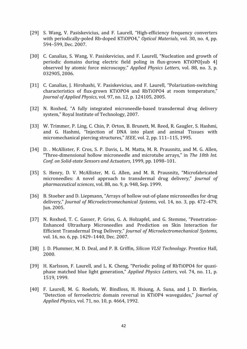
42
[29] S. Wang, V. Pasiskevicius, and F. Laurell, “High‐efficiency frequency converterswithperiodically‐poledRb‐dopedKTiOPO4,”OpticalMaterials,vol.30,no.4,pp.594–599,Dec.2007.
[30] C. Canalias, S.Wang,V. Pasiskevicius, andF. Laurell, “Nucleation andgrowthofperiodic domains during electric field poling in flux‐grown KTiOPO[sub 4]observed by atomic forcemicroscopy,”AppliedPhysicsLetters, vol. 88, no. 3, p.032905,2006.
[31] C. Canalias, J.Hirohashi, V. Pasiskevicius, andF. Laurell, “Polarization‐switchingcharacteristics of flux‐grown KTiOPO4 and RbTiOPO4 at room temperature,”JournalofAppliedPhysics,vol.97,no.12,p.124105,2005.
[32] N. Roxhed, “A fully integrated microneedle‐based transdermal drug deliverysystem,”RoyalInstituteofTechnology,2007.
[33] W.Trimmer,P.Ling,C.Chin,P.Orton,B.Brunett,M.Reed,R.Gaugler,S.Hashmi,and G. Hashmi, “Injection of DNA into plant and animal Tissues withmicromechanicalpiercingstructures,”IEEE,vol.2,pp.111–115,1995.
[34] D. .McAllister, F. Cros, S. P.Davis, L.M.Matta,M.R. Prausnitz, andM.G.Allen,“Three‐dimensionalhollowmicroneedle andmicrotubearrays,” inThe10th Int.Conf.onSolid‐stateSensorsandActuators,1999,pp.1098–101.
[35] S. Henry, D. V. McAllister, M. G. Allen, and M. R. Prausnitz, “Microfabricatedmicroneedles: A novel approach to transdermal drug delivery,” Journal ofpharmaceuticalsciences,vol.88,no.9,p.948,Sep.1999.
[36] B.StoeberandD.Liepmann,“Arraysofhollowout‐of‐planemicroneedlesfordrugdelivery,” JournalofMicroelectromechanicalSystems,vol.14,no.3,pp.472–479,Jun.2005.
[37] N. Roxhed, T. C. Gasser, P. Griss, G. A. Holzapfel, and G. Stemme, “Penetration‐Enhanced Ultrasharp Microneedles and Prediction on Skin Interaction forEfficientTransdermalDrugDelivery,”JournalofMicroelectromechanicalSystems,vol.16,no.6,pp.1429–1440,Dec.2007.
[38] J.D.Plummer,M.D.Deal,andP.B.Griffin,SiliconVLSITechnology.PrenticeHall,2000.
[39] H.Karlsson,F.Laurell, andL.K.Cheng, “PeriodicpolingofRbTiOPO4 forquasi‐phasematchedblue light generation,”AppliedPhysicsLetters, vol. 74, no. 11, p.1519,1999.
[40] F. Laurell, M. G. Roelofs, W. Bindloss, H. Hsiung, A. Suna, and J. D. Bierlein,“Detection of ferroelectric domain reversal in KTiOP4 waveguides,” Journal ofAppliedPhysics,vol.71,no.10,p.4664,1992.

43
[41] G.D.Boyd,“ParametricInteractionofFocusedGaussianLightBeams,”JournalofAppliedPhysics,vol.39,no.8,p.3597,1968.
[42] W.Wiechmann,S.Kubota,T.Fukui,andH.Masuda,“Refractive‐indextemperaturederivatives of potassium titanyl phosphate.,” Optics letters, vol. 18, no. 15, pp.1208–10,Aug.1993.
[43] H.VanherzeeleandJ.D.Bierlein,“Magnitudeofthenonlinear‐opticalcoefficientsofKTiOPO4.,”Opticsletters,vol.17,no.14,pp.982–4,Jul.1992.