Construction of uniform buried pn junctions on pyramid Si ...
27
Supporting Information Construction of uniform buried pn junctions on pyramid Si photocathodes using a facile and safe spin-on method for photoelectrochemical water splitting He Li ab , Bin Liu ab , Shijia Feng ab , Huimin Li ab , Tuo Wang *ab , Jinlong Gong ab a Key Laboratory for Green Chemical Technology of Ministry of Education, School of Chemical Engineering and Technology, Tianjin University, Tianjin 300072, China b Collaborative Innovation Center of Chemical Science and Engineering (Tianjin), Tianjin University, Tianjin 300072, China Corresponding Authors * E-mail: [email protected]; Fax: +86 22 87401818 Electronic Supplementary Material (ESI) for Journal of Materials Chemistry A. This journal is © The Royal Society of Chemistry 2019
Transcript of Construction of uniform buried pn junctions on pyramid Si ...

Supporting Information
Construction of uniform buried pn junctions
on pyramid Si photocathodes using a facile
and safe spin-on method for
photoelectrochemical water splitting
He Liab, Bin Liuab, Shijia Fengab, Huimin Liab, Tuo Wang*ab, Jinlong Gongab
a Key Laboratory for Green Chemical Technology of Ministry of Education, School of
Chemical Engineering and Technology, Tianjin University, Tianjin 300072, China
b Collaborative Innovation Center of Chemical Science and Engineering (Tianjin),
Tianjin University, Tianjin 300072, China
Corresponding Authors
*E-mail: [email protected]; Fax: +86 22 87401818
Electronic Supplementary Material (ESI) for Journal of Materials Chemistry A.This journal is © The Royal Society of Chemistry 2019

Materials
Ammonium dihydrogen phosphate (NH4H2PO4, ≥99.99%) was purchased from
Shanghai Aladdin Biochemical Technology. Ammonium hydroxide (NH4OH, 25.0%),
potassium hydroxide (KOH, ≥85.0%), hydrofluoric acid (HF, ≥40.0%) and
chloroplatinic acid ( H2PtCl6, ≥99.0%)were purchased from Tianjin Kemiou Chemical
Reagent Co., Ltd. Perchloric acid was supplied by Tianjin Xinqiao Chemical Trading
Co., Ltd. Hydrogen peroxide (H2O2, ≥30.0%) was purchased from Tianjin Jiangtian
Chemical Technology Co., Ltd. Hydrochloric acid (HCl, 36%-38%), concentrated
sulfuric acid (H2SO4, 95%-98%) and isopropyl alcohol (C3H8O, ≥%99.0%) were
purchased by Tianjin Yuanli Chemical Co., Ltd. Titanium (IV)i-propoxide (TTIP,
99.999%) was supplied by Suzhou Fornano Electronics Technology Co., Ltd. High
purity water (18.25 MΩꞏcm) supplied by a UP Water Purification System was used in
the whole experimental processes. Single-crystalline p-Si (100) wafers (one-side
polished) with a starting thickness of 500 μm, diameter of 4 inches and resistivity of 1-
10 Ω cm were obtained from Hefei Kejing Material Technology Co., Ltd. The SOD
polymer solution used here is dopant P 509 which was commercially available from
Filmtronics Co. (USA). The proton exchange membrane used in our work to separate
two electrolytes is Nafion-115 from DuPont.
Wet etching
The pyramidal surface textured (pyramid) silicon substrate was produced by a
chemical etching method. First of all, the Si wafer was boiled and cleaned with a full
Radio Corporation of America (RCA) cleaning method (RCA1: NH4OH: H2O2: H2O =
1:1:5 for 10 minutes at 70 ˚C; RCA2: HCL: H2O2: H20 = 1:1:6 for 10 minutes at 70 ˚C).
The purpose of the RCA cleaning is to remove the attached particles, organic matters
and metal ions from the surface of the wafer. The randomly distributed pyramid Si was

then fabricated through anisotropic etching in a mixture solution of potassium
hydroxide (KOH) (6 wt%) and isopropanol (3 vol%) at 80 °C for 25 min. The magnetic
stir bar was maintained in constant rotation during the etching process to maintain the
uniformity of temperature and concentration. After that, the sample was removed and
cleaned again as in the first step. Finally, the wafer was rinsed with high purity water
and blow-dried with nitrogen.
Fabrication of pn+Si
In this work, ADP aqueous solution as the phosphorous dopant source was
prepared by dissolving ADP in high purity water, concentration is 5 wt%. The ADP
aqueous solution was spun onto the front side of Si wafer at a speed of 4000 rpm,
followed by baking at 100 ˚C for 10 minutes. Subsequently, the Si wafer spin-coated
with ADP aqueous solution was annealed in an open quartz tube furnace at 950 ˚C for
1 hour. The formulas are as follows:
2 NH H PO∆→ P O 3H O 2NH (1)
2P O 5Si∆→ 4P ↓ 5SiO (2)
After the annealing process, the residual phosphosilicate glass was removed
entirely with 5 vol% HF solution at room temperature for 3 minutes. The process of
using SOD polymer solution as phosphorous dopant source was same as described
above while the spin speed was 3000 rpm according to its instruction manual.
Aluminum back contact was produced by depositing Al film onto the back side of Si
wafers and then annealing in N2 atmosphere at 800 ˚C for 10 minutes. Al film was
deposited by using direct current (DC) magnetron sputtering with a working power of
40 W for 20 minutes.
Atomic layer deposition of TiO2 thin film

TiO2 thin film was deposited onto pyramid pn+Si at 250˚C in a home-made atomic
layer deposition (ALD) system using TTIP and H2O as precursors. The precursors were
held at 70 ˚C and 25 ˚C respectively. One ALD cycle consists of TTIP dose for 3 s, N2
purge for 8 s, water dose for 0.2 s and N2 (Air Liquid) purge for 8 s. 670 cycles of TiO2
were deposited onto pyramid pn+Si. The ALD TiO2 growth on p-Si (100) substrate was
measured by the M-2000 spectroscopic ellipsometer (J.A. Woollam).
Cocatalyst deposition
In order to enhance the kinetics for water reduction reaction, Pt nanoparticles were
deposited by photo-electrodeposition until 50 mC passed through the Si electrode. The
photo-electrodeposition is performed at an applied potential of 0 V vs. Ag/AgCl (3 M
KCl) on the work electrode under simulated AM 1.5G illumination. The electrolyte was
1 mM aqueous solution of H2PtCl6 (using H2SO4 adjusts to pH < 1). The Si back side
was attached with a cooper belt using conductive silver paint and the entire electrode
was encapsulated with epoxy on slide glass before platinization. The active area without
covered by epoxy was determined by a digital camera and ImageJ software.
Photoanode construction
The BiVO4 film was synthesized on FTO substrates by metalorganic
decomposition (MOD) method using dimethyl sulfoxide (DMSO) as the solvent to
dissolve both Bi and V precursors simultaneously. 0.2425 g bismuth nitrate
pentahydrate Bi(NO3)3ꞏ5H2O and 0.1325 g vanadyl acetylacetonate VO(acac)2 are
mixed in 500 µL DMSO and sonicated for 30 min at room temperature. FTO substrate
is preheated on the hotplate at 60 °C, and the film is deposited onto FTO by spin coating
at 1000 rpm for 20 s followed by 3000 rpm for 40 s. Then the samples were calcined in
a tube furnace at 500 °C for 2 h in the air. The obtained samples were soaked in 1 M
KOH for 5 min to remove the surface VOx species. Finally, BiVO4 photoanode was

immersed in 1 M KBi buffer solution containing 0.2 M Na2SO3 with simulated AM 1.5
G illumination for 10 min, during which photo-induced etching of the surface region of
amorphous BiVO4 is removed to obtain enhanced surface oxygen vacancies.
CoOx nanoparticles were synthesized by a typical hydrothermal method. In a
typical procedure, 0.4 mL ammonium solution (NH3ꞏH2O, 25 wt%) was added into 25
mL 1 mM cobalt acetate ethanol solution, followed by stirring for 15 min. Then the
solution was transferred to a 50 mL Teflon-lined stainless steel autoclave. The
hydrothermal synthesis was conducted at 120 ˚C for 1 h. The obtained products were
centrifuged, washed with deionized water and ethanol for three times, respectively.
Lastly, the obtained samples were dried in 80 ˚C for 12 h in a drying oven. The
BiVO4/CoOx photoanode was fabricated by a drop-casting technique. Firstly, 20 mg of
CoOx nanoparticles were dispersed in 100 mL absolute ethanol and sonicated for 30
min to form a uniform nanoparticle “ink”. Then 100 µL “ink” was drop-casted onto a
1 cm2 BiVO4 electrode. The composites were fully dried at 80 ˚C for 30 min and then
annealed at 450 ˚C for 2 h1.
Structural and optical characterization
The morphology and microstructure of the samples were characterized using a
field emission scanning electron microscope (FE-SEM, Hitachi S-4800, 5 kV) with an
energy-dispersive X-ray (EDX) detector. The light absorption of as-prepared samples
was obtained using a Shimadzu UV-2550 spectrophotometer equipped with an
integrating sphere using BaSO4 as the reflectance standard. Steady-state
photoluminescence (PL) spectroscopy was performed on Hitachi F-4600 fluorescence
spectrophotometer with 238 nm as the excitation wavelength. X-ray photoemission
spectroscopy (XPS) analysis of the samples was carried out on a Physical Electronics

PHI 1600 ESCA system with an Al Kα X-ray source (1486.6 eV). The binding energy
was calibrated using the C 1s photoelectron peak at 284.6 eV.
Photoelectrochemical (PEC) measurements
The PEC performance of the Si photocathode was evaluated in a three-electrode
configuration, with the Si photocathode as the working electrode, Ag/AgCl/sat. KCl as
the reference electrode and a platinum foil (2 cm 2 cm) as the counter electrode. 1
M HClO4 (pH 0) aqueous solution was used as the electrolyte. Before PEC tests, the
electrolyte was purged with N2 (Air Liquide) for around 10 minutes to remove
dissolved O2. The potentials obtained from each measurement were converted into
values against reversible hydrogen electrode (RHE) using Nernst Equation. An
electrochemical workstation (CompactStat. E202050, IVIUM) was used in all PEC
measurements. The linear sweep voltammetry (J-V plots), with a scan rate of 50 mV s-
1 and chronoamperometry (stability tests) of samples were measured under the
irradiation of a 300 W Xenon lamp (Beijing Perfectlight Technology Co Lt, LS-
SXE300CUV) equipped with an AM 1.5G filter (100mW cm-2). During the 250 h
stability test, contamination was observed at the bottom of the porous ceramic plug of
the reference electrode, which could be caused by the transfer of electrolyte from the
reference electrode2, 3.
The applied bias photon-to-current efficiency (ABPE) of above photocathodes
was calculated by using the J-V curves with an assumption of 100% Faradic efficiency,
according to the following equation:
ABPE 100% (3)
where Vapp is the applied potential (vs. RHE), Jph is the photocurrent density (mA cm-2)
under AM 1.5G irradiation, and P is the incident illumination intensity (mW cm-2) (100
mW cm-2 in this work).

The IPCE was measured under monochromatic illumination from a 150 W Xe lamp
(Zolix LSH-X150) equipped with monochromator (Omni-𝜆 300) at 0 V vs. RHE using
the equation:
IPCE % 100% (4)

Supplementary Figures:
Fig. S1 P 2p XPS spectrum of pn+Si sample, which could be deconvoluted into 134.2 eV and 135.3 eV for P2O5 and P4O10
4, respectively.

Fig. S2 (a) (b) side and top view SEM images of pristine pyramid Si; (c) (d) side and top view SEM images of pyramid Si after spin coating ADP aqueous solution and annealing.

Fig. S3 Top view SEM images and EDX elemental mapping of pyramid Si spin coated with (a, b) ADP aqueous solution, and (c, d) SOD polymer solution; Side view SEM images and EDX elemental mapping of pyramid Si spin coated with (e, f) ADP aqueous solution, and (g, h) SOD polymer solution.

Fig. S4 EDX spectra of (a) top and (b) side view of pyramid Si spin coated by ADP aqueous solution; (c) top and (d) side view of pyramid Si spin coated by SOD polymer solution.

Fig. S5 (a) Top and (b) side view of pyramid p-Si spin coated using 85 wt% H3PO4.
Pyramid p-Si substrate spin coated using 85 wt% H3PO4, which of much higher
viscosity (about 30 times that of ADP aqueous solution) than ADP aqueous solution
and SOD polymer solution, was completely covered by a thick layer of dopant.

Fig. S6 (a) The optimization of spin speed for pyramid pn+Si/Pt photocathodes spin coated with (a) ADP aqueous solution, and (b) SOD polymer solution, measured in 1 M HClO4 (pH = 0) under AM 1.5G illumination.

Fig. S7 The open circuit potential versus time of pyramid pn+Si(ADP)/Pt and pn+Si(SOD)/Pt photocathodes in the dark and under AM 1.5G illumination, in 1 M HClO4 (pH = 0) electrolyte.
The photovoltage was determined from the difference of open circuit potentials of
the sample in the dark and under illumination, respectively5. The open circuit potential
was measured by monitoring the resting potential of samples (vs. the reference
electrode) in the open circuit condition, with the illumination turned on and off
manually. The duration of illumination on and off were both 10 s, respectively.

Fig. S8 J-V curves of planar and pyramid pn+Si/Pt doped by ADP aqueous solution and SOD polymer solution separately. All the measurements are measured in 1 M HClO4 (pH = 0) under AM 1.5G illumination.

Fig. S9 UV-vis reflection plot of planar and pyramid Si and pyramid Si/TiO2 photocathodes.

Fig. S10 Stability of four pn+Si(ADP)/TiO2/Pt samples from different batches
To thoroughly evaluate the stability of the sample with the batch-to-batch variation
considered, four pn+Si(ADP)/TiO2/Pt samples from different batches were measured.
Two of the samples showed a 250 h stability, while the other two exhibited stabilities
of 30 h and 80 h, respectively. The variation of stability might be attributed to the
presence of dust particles from the ambient before transferring the sample to the ALD
chamber, which results in the formation of pin-holes in TiO2 protective layer. Therefore,
pn+Si(ADP)/TiO2/Pt sample is capable of reaching a reproducible stability of 250 h.

Fig. S11 SEM images of the pn+Si(ADP)/TiO2/Pt sample, (a) before stability test, (b) after J-V test and (c) after 250 h long term stability test at 0.2 V vs. RHE in 1 M HClO4 electrolyte (pH 0) under simulated AM 1.5G illumination.

Fig. S12 J-V curves of pn+Si/TiO2/Pt photocathode before and after long term stability test in 1 M HClO4 (pH = 0) under AM 1.5G illumination.
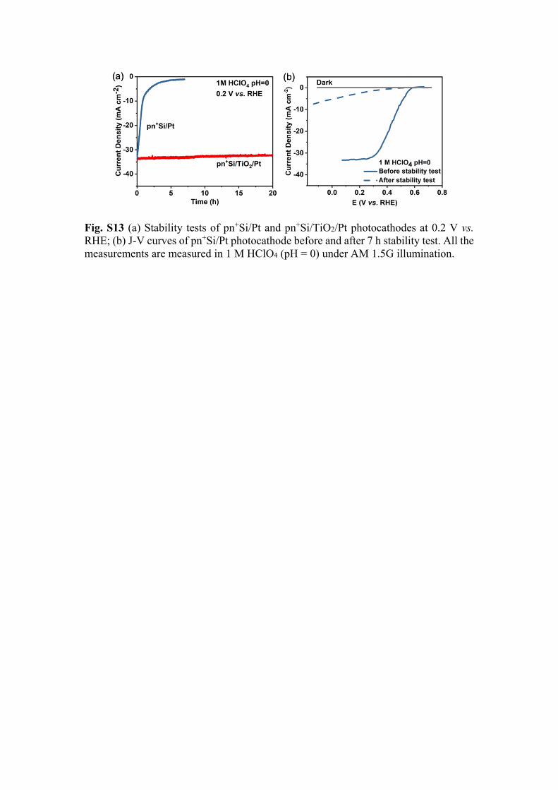
Fig. S13 (a) Stability tests of pn+Si/Pt and pn+Si/TiO2/Pt photocathodes at 0.2 V vs. RHE; (b) J-V curves of pn+Si/Pt photocathode before and after 7 h stability test. All the measurements are measured in 1 M HClO4 (pH = 0) under AM 1.5G illumination.

Fig. S14 Performance comparison of pn+Si photocathodes using different diffusion methods and dopants for PEC HER versus onset potential. (Details in Table S3, with sample numbers representing the symbols in Fig. S14)

Fig. S15 J-V curves of Si HIT solar cell and Si HIT solar cell behind a BiVO4 photoanode under AM 1.5G illumination.

Fig. S16 Schematic illustration of HIT-pn+Si(ADP)/TiO2/Pt photocathode and BiVO4/CoOx photoanode tandem cell, with illumination area (yellowish shade) and active area (with bubbles) marked; Si HIT solar cell and pn+Si(ADP)/TiO2/Pt were connected in series using InGa alloy and Cu wire (Si HIT solar cell, Cu and edge of pn+Si(ADP)/TiO2/Pt were encapsulated with epoxy).
For the two-electrode tandem cell (Fig. 6b and d), the illumination area of the
optimized tandem cell was defined by the area of BiVO4/CoOx photoanode in direct
contact with the electrolyte (0.92 cm2), which is placed in front of the smaller (0.86
cm2) Pt/TiO2/pn+Si(ADP)/InGa/Cu/InGa/HIT photocathode (pn+Si(ADP)/TiO2/Pt is
0.44 cm2 and Si HIT is 0.42 cm2). For the three-electrode configuration (Fig. 6a and c),
the illumination area was defined by the photoanode (0.92 cm2) and photocathode (0.86
cm2), respectively, as in normal PEC measurements. The active area of the tandem cell
was the area where OER and HER take place (0.92 cm2 for photoanode and 0.44 cm2
photocathode). All the areas were measured and calibrated by the Image J software.
When calculating current densities for the two-electrode tandem cell (Fig. 6b and
d), the largest illumination cross-section (0.92 cm2 of the BiVO4/CoOx photoanode)
was used as the denominator. For the three-electrode configuration (Fig. 6a and c), the
illumination area (0.92 cm2 for photoanode and 0.86 cm2 photocathode), rather than the
active area, was used as the denominator. The STH efficiency was calculated based on
these photocurrent densities.

Supplementary Tables:
Table. S1 Viscosity of tested samples.
Sample
Time/s Viscosity/cP 1 2 3 4 5 Average
1 H2O 77.56 77.74 77.98 78.22 78.16 77.93 0.8937
2 ADP aqueous
solution 84.67 85.06 85.07 85.72 85.59 85.22 1.0262
3 SOD polymer
solution 158.90 161.08 161.78 161.56 162.63 161.69 1.5790
The viscosity (η) of above samples was calculated according to the following equation:
η ηρρ
where ρ is the density (g cm-3), t is the time (s) obtained. Ubbelohde viscometer was
used in this test at the temperature of 25 ˚C.
(ρ 0.997 g cm , ρ 1.047 g cm , ρ 0.849 g cm )
Range of η given by our supplier is 1.45-1.82 cP (dopants with various
concentration of alcohol) at 25 ˚C.

Table. S2 Counts of P peaks in EDX spectrums.
Sample P counts Full-scale counts Atomic concentration/%
ADP (top view) 96 3718 2.58
ADP (side view) 83 4789 1.73
SOD (top view) 367 4213 8.71
SOD (side view) 177 3644 4.86

Table. S3 Performance comparison of pn+Si photocathodes using different diffusion methods and dopants for PEC HER.
# YearPhosphorous
source Morphology
Photoelectrode structure
E(onset) (V vs. RHE)
ABPE (%) Stability (h) Electrolyte Ref
This work 2019ADP aqueous
solution pyramid pn+Si/TiO2/Pt 0.58 10.6 250 1 M HClO4
1 2015SOD polymer
solution microwire pn+Si/Pt 0.51 5 - 0.5 M H2SO4 6
2 2018SOD polymer
solution microwire pn+Si/NiSi/NiMo 0.55 10.1 288 1 M KOH 7
3 2011 CeP5O14 planar pn+Si/Pt 0.56 9.6 - 0.5 M H2SO4 8
4 2015 PClO3 pyramid pn+Si/Al2O3/Pt 0.52 6.8 100 0.5 M
K2SO4+0.5 M H2SO4
9
5 2015 PClO3 microwire pn+Si/Pt 0.44 2.9 - 0. 5 M H2SO4 10
6 2016 PClO3 pyramid pn+Si/Pt@SiO2 0.49 8.9 22 0.5 M
K2SO4+0.5 M H2SO4
11
7 2017 PClO3 pyramid pn+Si/Pt2/TiO2 0.56 10.5 168 1 M HClO4 12

Supplementary References:
1. X. Chang, T. Wang, P. Zhang, J. Zhang, A. Li and J. Gong, J. Am. Chem. Soc., 2015, 137, 8356-8359.
2. M. P. Mousavi and P. Buhlmann, Anal. Chem., 2013, 85, 8895-8901. 3. A. Yakushenko, D. Mayer, J. Buitenhuis, A. Offenhausser and B. Wolfrum, Lab
Chip, 2014, 14, 602-607. 4. A. Thøgersen, M. Syre, B. Retterstol laisen and S. Diplas, J. Appl. Phys., 2013,
113, 044307. 5. L. Ji, M. D. McDaniel, S. Wang, A. B. Posadas, X. Li, H. Huang, J. C. Lee, A. A.
Demkov, A. J. Bard, J. G. Ekerdt and E. T. Yu, Nat. Nanotechnol., 2014, 10, 84-90.
6. M. R. Shaner, J. R. McKone, H. B. Gray and N. S. Lewis, Energy Environ. Sci.,2015, 8, 2977-2984.
7. W. Vijselaar, R. M. Tiggelaar, H. Gardeniers and J. Huskens, ACS Energy Lett., 2018, 1086-1092.
8. S. W. Boettcher, E. L. Warren, M. C. Putnam, E. A. Santori, D. Turner-Evans, M. D. Kelzenberg, M. G. Walter, J. R. McKone, B. S. Brunschwig, H. A. Atwater and N. S. Lewis, J. Am. Chem. Soc., 2011, 133, 1216-1219.
9. R. Fan, W. Dong, L. Fang, F. Zheng, X. Su, S. Zou, J. Huang, X. Wang and M. Shen, Appl. Phys. Lett., 2015, 106.
10. C. W. Roske, E. J. Popczun, B. Seger, C. G. Read, T. Pedersen, O. Hansen, P. C. K. Vesborg, B. S. Brunschwig, R. E. Schaak, I. Chorkendorff, H. B. Gray and N. S. Lewis, J. Phys. Chem. Lett., 2015, 6, 1679-1683.
11. R. Fan, C. Tang, Y. Xin, X. Su, X. Wang and M. Shen, Appl. Phys. Lett., 2016, 109, 233901.
12. R. Fan, W. Dong, L. Fang, F. Zheng and M. Shen, J. Mater. Chem. A, 2017, 5, 18744-18751.