Computer Structure 2012 – Uncore 1 Computer Structure The Uncore.
Upload
lynette-gallagherCategory
view
216download
0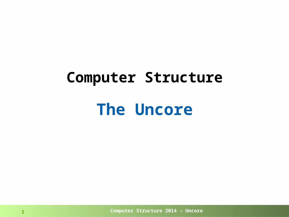
Computer Structure 2014 – Uncore1
Computer Structure
The Uncore
Computer Structure 2014 – Uncore2
Personal Computer System
Graphics
Core LLCCore LLC
Core LLCCore LLC
System Agent
Display
DMI PCIe
IMC
PCIe ×16
2ch DDR3
PCHPlatform Controller Hub
DMI×4FDI
HDMI
DisplayPort
SATA
SATABIOS
Audio CodecLine outMic
USBUSB
Computer Structure 2014 – Uncore3
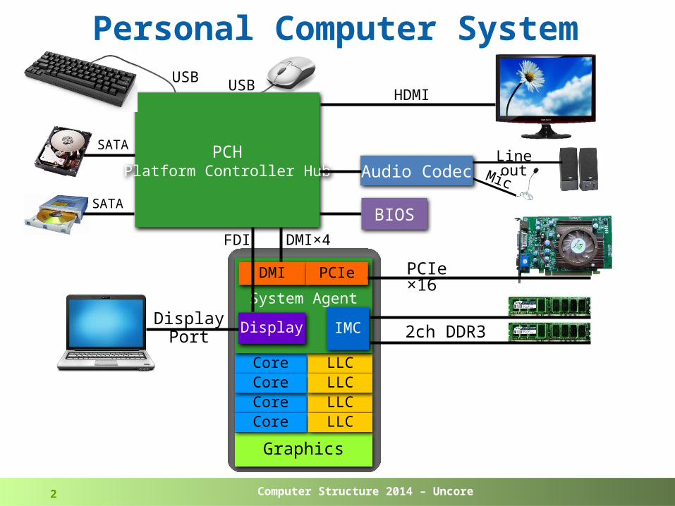
3rd Generation Intel CoreTM
· 22nm process· Quad core die, with Intel HD Graphics 4000· 1.4 Billion transistors· Die size: 160 mm2
Computer Structure 2014 – Uncore4
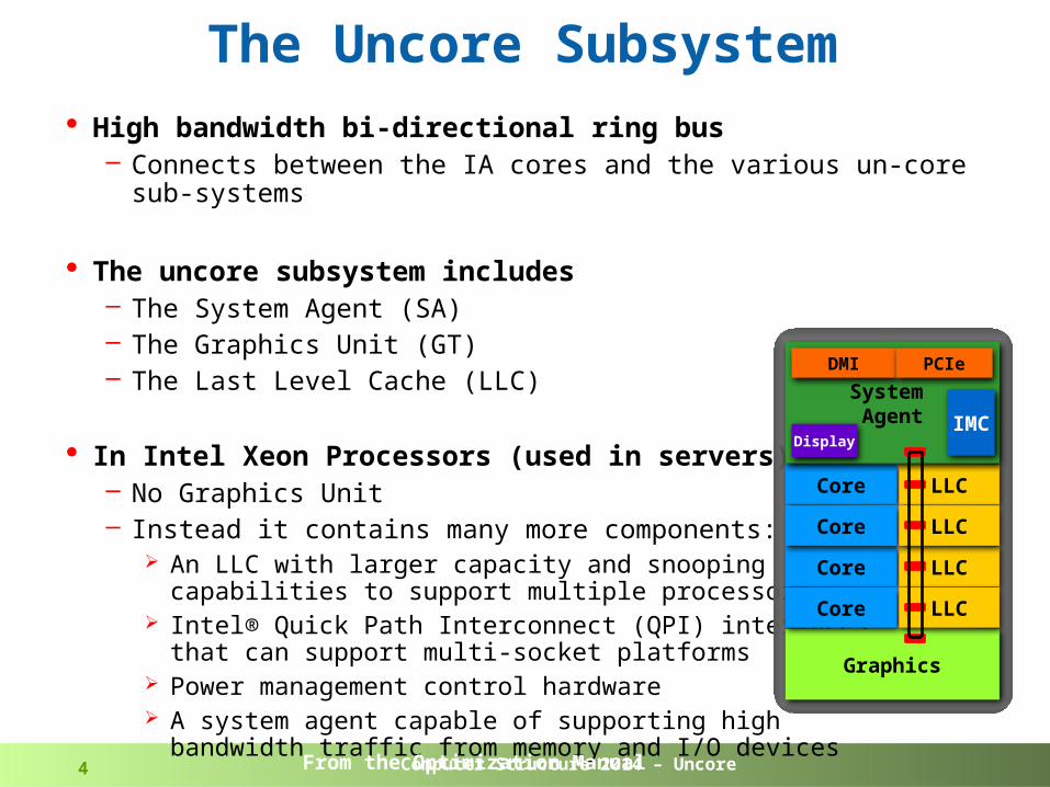
The Uncore Subsystem· High bandwidth bi-directional ring bus
– Connects between the IA cores and the various un-core sub-systems
· The uncore subsystem includes – The System Agent (SA)– The Graphics Unit (GT) – The Last Level Cache (LLC)
· In Intel Xeon Processors (used in servers)– No Graphics Unit – Instead it contains many more components:
An LLC with larger capacity and snooping capabilities to support multiple processors
Intel® Quick Path Interconnect (QPI) interfaces that can support multi-socket platforms
Power management control hardware A system agent capable of supporting high
bandwidth traffic from memory and I/O devices
From the Optimization Manual
Graphics
Core LLC
Core LLC
Core LLC
Core LLC
System Agent
Display
DMI PCIe
IMC
Computer Structure 2014 – Uncore5
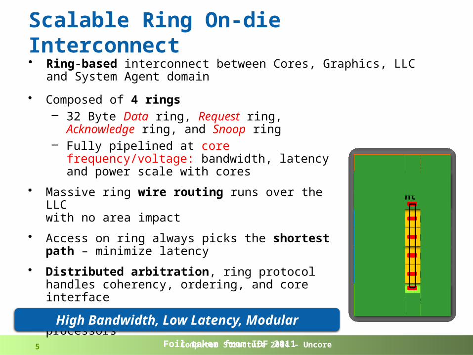
• Ring-based interconnect between Cores, Graphics, LLC and System Agent domain
Graphics
Core LLC
Core LLC
Core LLC
Core LLC
System AgentDisplay
DMIPCI
Express*
IMC
Scalable Ring On-die Interconnect
• Composed of 4 rings– 32 Byte Data ring, Request ring,
Acknowledge ring, and Snoop ring– Fully pipelined at core frequency/voltage:
bandwidth, latency and power scale with cores
• Massive ring wire routing runs over the LLC with no area impact
• Access on ring always picks the shortest path – minimize latency
• Distributed arbitration, ring protocol handles coherency, ordering, and core interface
• Scalable to servers with large number of processors
High Bandwidth, Low Latency, Modular
Foil taken from IDF 2011
Computer Structure 2014 – Uncore6
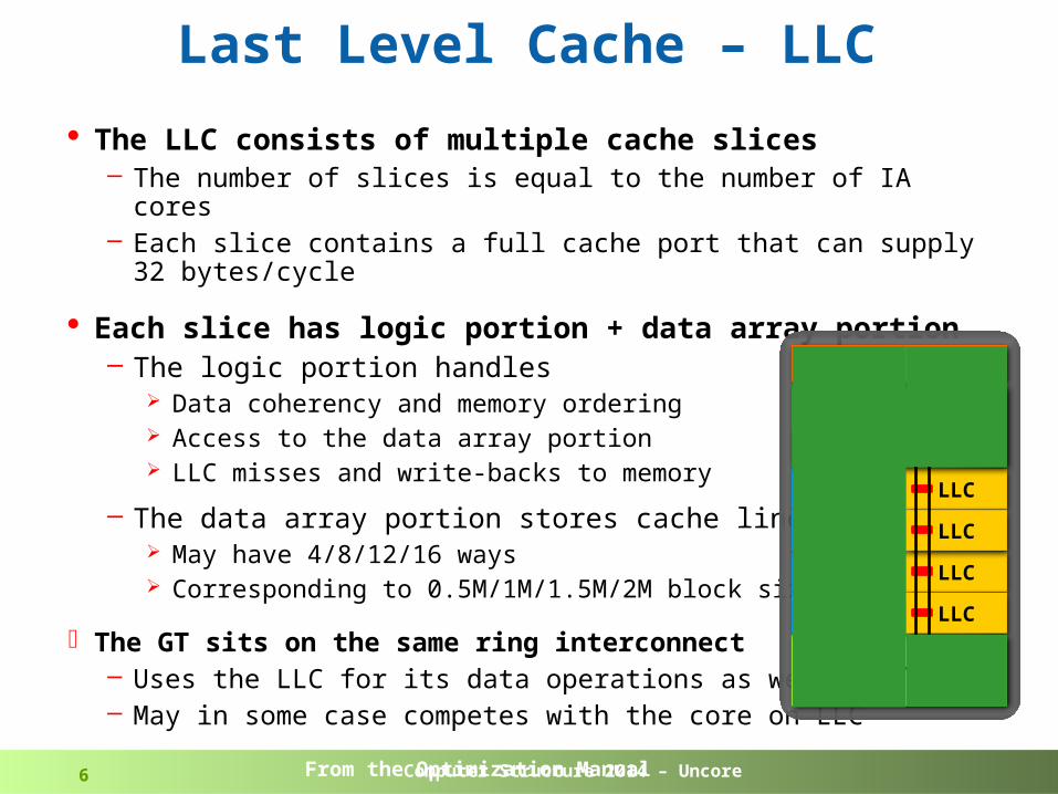
Last Level Cache – LLC
· The LLC consists of multiple cache slices– The number of slices is equal to the number of IA cores– Each slice contains a full cache port that can supply 32 bytes/cycle
· Each slice has logic portion + data array portion– The logic portion handles
Data coherency and memory ordering Access to the data array portion LLC misses and write-backs to memory
– The data array portion stores cache lines May have 4/8/12/16 ways Corresponding to 0.5M/1M/1.5M/2M block size
· The GT sits on the same ring interconnect– Uses the LLC for its data operations as well– May in some case competes with the core on LLC
From the Optimization Manual
Graphics
Core LLC
Core LLC
Core LLC
Core LLC
System AgentDisplay
DMIPCI
Express*
IMC
Computer Structure 2014 – Uncore7
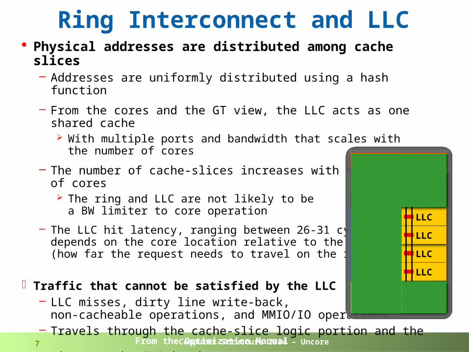
Ring Interconnect and LLC· Physical addresses are distributed among cache slices
– Addresses are uniformly distributed using a hash function
– From the cores and the GT view, the LLC acts as one shared cache With multiple ports and bandwidth that scales with the number of cores
– The number of cache-slices increases with the number of cores The ring and LLC are not likely to be
a BW limiter to core operation
– The LLC hit latency, ranging between 26-31 cycles,depends on the core location relative to the LLC block (how far the request needs to travel on the ring)
· Traffic that cannot be satisfied by the LLC– LLC misses, dirty line write-back,
non-cacheable operations, and MMIO/IO operations– Travels through the cache-slice logic portion and the
ring, to the IMC in the system agent
From the Optimization Manual
Graphics
Core LLC
Core LLC
Core LLC
Core LLC
System AgentDisplay
DMIPCI
Express*
IMC
Computer Structure 2014 – Uncore8
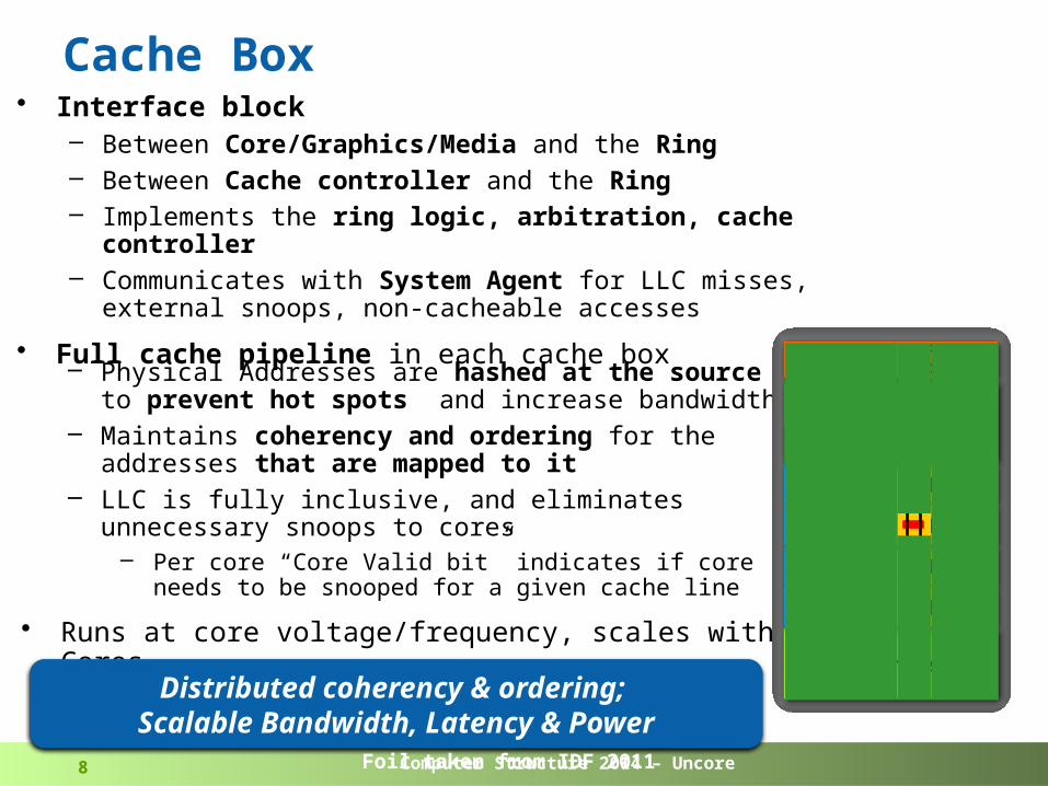
Cache Box• Interface block
– Between Core/Graphics/Media and the Ring– Between Cache controller and the Ring– Implements the ring logic, arbitration, cache controller– Communicates with System Agent for LLC misses,
external snoops, non-cacheable accesses
• Full cache pipeline in each cache box
– Physical Addresses are hashed at the source to prevent hot spots and increase bandwidth
– Maintains coherency and ordering for the addresses that are mapped to it
– LLC is fully inclusive, and eliminates unnecessary snoops to cores
– Per core “Core Valid bit” indicates if coreneeds to be snooped for a given cache line
• Runs at core voltage/frequency, scales with Cores
Distributed coherency & ordering; Scalable Bandwidth, Latency & Power
Foil taken from IDF 2011
Graphics
Core LLC
Core LLC
Core LLC
Core LLC
System AgentDisplay
DMIPCI
Express*
IMC
Computer Structure 2014 – Uncore9
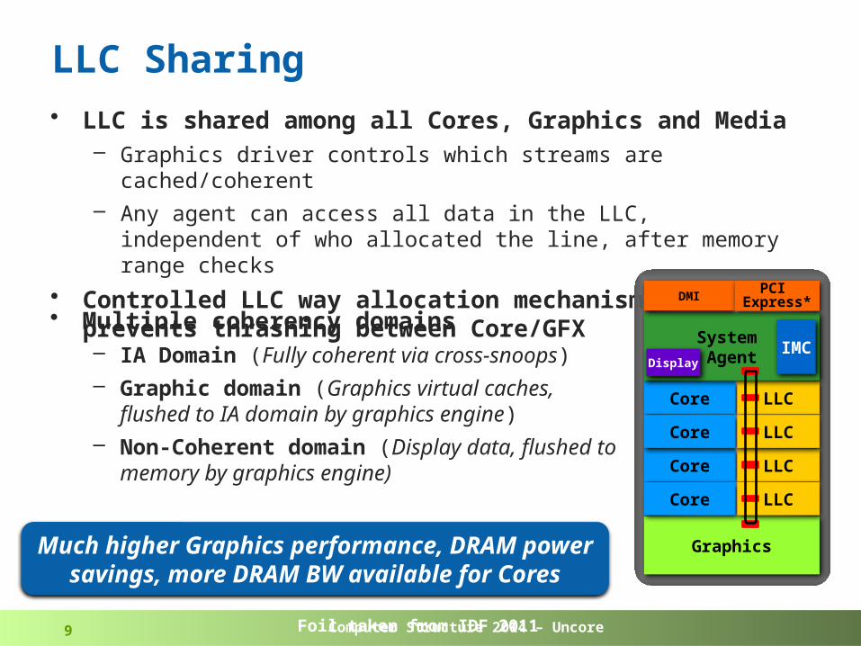
LLC Sharing• LLC is shared among all Cores, Graphics and Media
– Graphics driver controls which streams are cached/coherent– Any agent can access all data in the LLC, independent of who
allocated the line, after memory range checks
• Controlled LLC way allocation mechanism prevents thrashing between Core/GFX
Much higher Graphics performance, DRAM power savings, more DRAM BW
available for Cores
• Multiple coherency domains– IA Domain (Fully coherent via cross-snoops)– Graphic domain (Graphics virtual caches,
flushed to IA domain by graphics engine)– Non-Coherent domain (Display data,
flushed to memory by graphics engine)
Foil taken from IDF 2011
Graphics
Core LLC
Core LLC
Core LLC
Core LLC
System AgentDisplay
DMIPCI
Express*
IMC
Computer Structure 2014 – Uncore10
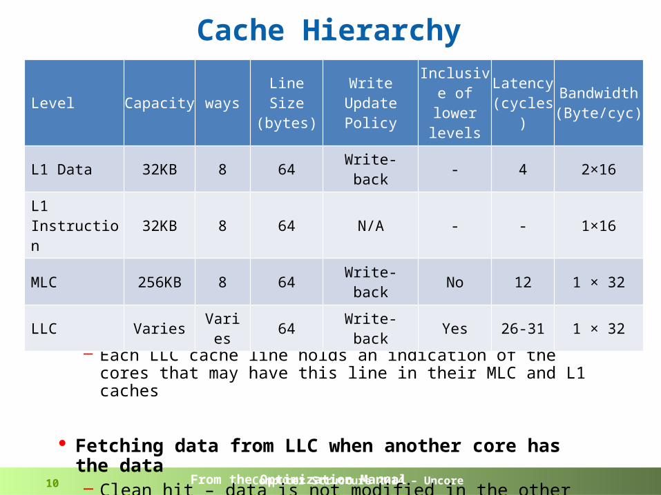
Cache Hierarchy
From the Optimization Manual
· The LLC is inclusive of all cache levels above it– Data contained in the core caches must also reside in the LLC– Each LLC cache line holds an indication of the cores that may have
this line in their MLC and L1 caches
· Fetching data from LLC when another core has the data– Clean hit – data is not modified in the other core – 43 cycles– Dirty hit – data is modified in the other core – 60 cycles
Level Capacity ways Line Size(bytes)
Write UpdatePolicy
Inclusive of lower levels
Latency(cycles)
Bandwidth(Byte/cyc)
L1 Data 32KB 8 64 Write-back - 4 2×16
L1 Instruction 32KB 8 64 N/A - - 1×16
MLC 256KB 8 64 Write-back No 12 1 × 32
LLC Varies Varies 64 Write-back Yes 26-31 1 × 32
Computer Structure 2014 – Uncore1111
GT
System Agent
iMPH MC DDRNCU
PEG/DMIIO
L3
L3
Core 0 L2
Core 1 L2
L2
AD
BL
AK
IV
DRd0
DRd1
DRdG
Hit
HitNo
Snoop
No Snoop
GO1
D21
D11
Hit No Snoop
GOG D2
G
D1G
GOG
D20
GO0D10
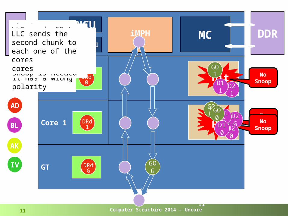
Core 0, Core 1 and the GFX issue data read requests
The GFX request was not sent to the ring in the current cycle, since it has a wrong polarity
The requests travel in the ring
The Core’s requests each get to the right LLC slice
Both Core’s requests get a it in the LLC, and the CVBs indicate that no snoop is needed
LLC sends GO to both cores to acknowledge that both cores can get the data
LLC sends the first chunk (1/2 cache line) to each one of the cores
LLC sends the second chunk to each one of the cores
Computer Structure 2014 – Uncore12
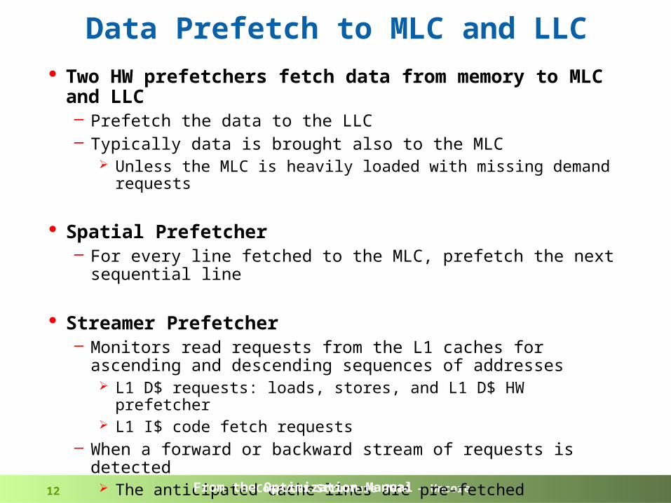
Data Prefetch to MLC and LLC· Two HW prefetchers fetch data from memory to MLC and LLC
– Prefetch the data to the LLC – Typically data is brought also to the MLC
Unless the MLC is heavily loaded with missing demand requests
· Spatial Prefetcher– For every line fetched to the MLC, prefetch the next sequential line
· Streamer Prefetcher– Monitors read requests from the L1 caches for ascending and
descending sequences of addresses L1 D$ requests: loads, stores, and L1 D$ HW prefetcher L1 I$ code fetch requests
– When a forward or backward stream of requests is detected The anticipated cache lines are pre-fetched Cannot cross 4K page boundary (same physical page)
From the Optimization Manual
Computer Structure 2014 – Uncore13
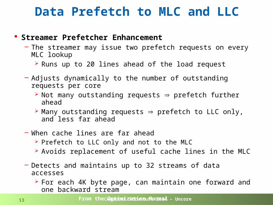
Data Prefetch to MLC and LLC
· Streamer Prefetcher Enhancement– The streamer may issue two prefetch requests on every MLC lookup
Runs up to 20 lines ahead of the load request
– Adjusts dynamically to the number of outstanding requests per core Not many outstanding requests prefetch further ahead Many outstanding requests prefetch to LLC only, and less far ahead
– When cache lines are far ahead Prefetch to LLC only and not to the MLC Avoids replacement of useful cache lines in the MLC
– Detects and maintains up to 32 streams of data accesses For each 4K byte page, can maintain one forward and one backward
stream
From the Optimization Manual
Computer Structure 2014 – Uncore14
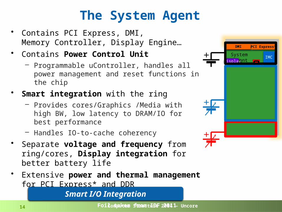
The System Agent• Contains PCI Express, DMI,
Memory Controller, Display Engine…• Contains Power Control Unit
– Programmable uController, handles all power management and reset functions in the chip
• Smart integration with the ring– Provides cores/Graphics /Media with high BW,
low latency to DRAM/IO for best performance– Handles IO-to-cache coherency
• Separate voltage and frequency from ring/cores, Display integration for better battery life
• Extensive power and thermal management for PCI Express* and DDR
Smart I/O Integration
Graphics
Core LLC
Core
Core LLC
Core LLC
System Agent Display
DMI PCI Express*
IMC
LLC
Foil taken from IDF 2011
Computer Structure 2014 – Uncore15
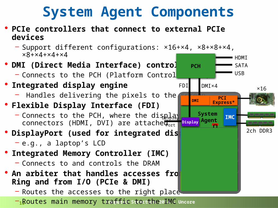
System Agent Components· PCIe controllers that connect to external PCIe devices
– Support different configurations: ×16+×4, ×8+×8+×4, ×8+×4+×4+×4· DMI (Direct Media Interface) controller
– Connects to the PCH (Platform Controller Hub)· Integrated display engine
– Handles delivering the pixels to the screen· Flexible Display Interface (FDI)
– Connects to the PCH, where the display connectors (HDMI, DVI) are attached
· DisplayPort (used for integrated display)– e.g., a laptop’s LCD
· Integrated Memory Controller (IMC)– Connects to and controls the DRAM
· An arbiter that handles accesses from Ring and from I/O (PCIe & DMI)– Routes the accesses to the right place– Routes main memory traffic to the IMC
2ch DDR3
×16 PCIe
Graphics
Core LLC
Core LLC
Core LLC
Core LLC
System AgentDisplay
DMIPCI
Express*
IMC
PCH
DMI×4FDI
HDMI
SATA
USB
Display
Port
Computer Structure 2014 – Uncore16
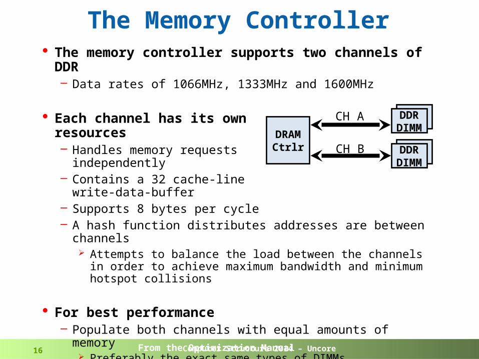
The Memory Controller· The memory controller supports two channels of DDR
– Data rates of 1066MHz, 1333MHz and 1600MHz
· Each channel has its own resources – Handles memory requests
independently– Contains a 32 cache-line
write-data-buffer– Supports 8 bytes per cycle– A hash function distributes addresses are between channels
Attempts to balance the load between the channels in order to achieve maximum bandwidth and minimum hotspot collisions
· For best performance– Populate both channels with equal amounts of memory
Preferably the exact same types of DIMMs– Use highest supported speed DRAM, with the best DRAM timings
From the Optimization Manual
CH A DDRDIMM
DDRDIMM
CH BDRAMCtrlr
Computer Structure 2014 – Uncore17
The Memory Controller· High-performance out-of-order scheduler
– Attempts to maximize memory bandwidth while minimizing latency– Writes to the memory controller are considered completed when they are
written to the write-data-buffer– The write-data-buffer is flushed out to main memory at a later time, not
impacting write latency
· Partial writes are not handled efficiently on the memory controller – May result in read-modify-write operations on the DDR channel
if the partial-writes do not complete a full cache-line in time– Software should avoid creating partial write transactions whenever possible
E.g., buffer the partial writes into full cache line writes
· iMC also supports high-priority isochronous requests – E.g., USB isochronous, and Display isochronous requests
· High bandwidth of memory requests from the integrated display engine takes up some of the memory bandwidth – Impacts core access latency to some degree
From the Optimization Manual
Computer Structure 2014 – Uncore18
Integration: Optimization Opportunities• Dynamically redistribute power between Cores & Graphics
• Tight power management control of all components, providing better granularity and deeper idle/sleep states
• Three separate power/frequency domains: System Agent (Fixed), Cores+Ring, Graphics (Variable)
• High BW Last Level Cache, shared among Cores and Graphics– Significant performance boost, saves memory bandwidth and power
• Integrated Memory Controller and PCI Express ports– Tightly integrated with Core/Graphics/LLC domain– Provides low latency & low power – remove intermediate busses
• Bandwidth is balanced across the whole machine, from Core/Graphics all the way to Memory Controller
• Modular uArch for optimal cost/power/performance– Derivative products done with minimal effort/time
Foil taken from IDF 2011
Computer Structure 2014 – Uncore19
DRAM
Computer Structure 2014 – Uncore20
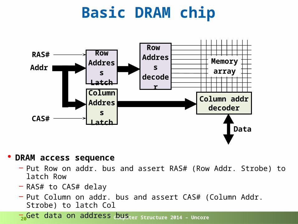
Basic DRAM chip
· DRAM access sequence– Put Row on addr. bus and assert RAS# (Row Addr. Strobe) to latch Row– RAS# to CAS# delay– Put Column on addr. bus and assert CAS# (Column Addr. Strobe) to latch Col– Get data on address bus
Row Address
Latch
Row Addressdecoder
Column addrdecoder
CAS#
RAS#
Data
MemoryarrayAddr
ColumnAddress
Latch
Computer Structure 2014 – Uncore21
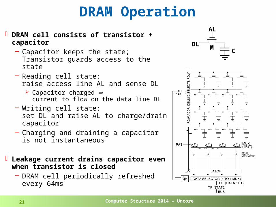
DRAM Operation· DRAM cell consists of transistor + capacitor
– Capacitor keeps the state;Transistor guards access to the state
– Reading cell state: raise access line AL and sense DL
Capacitor charged current to flow on the data line DL
– Writing cell state: set DL and raise AL to charge/drain capacitor
– Charging and draining a capacitor is not instantaneous
· Leakage current drains capacitor even when transistor is closed– DRAM cell periodically refreshed every 64ms
AL
DLCM
Computer Structure 2014 – Uncore22
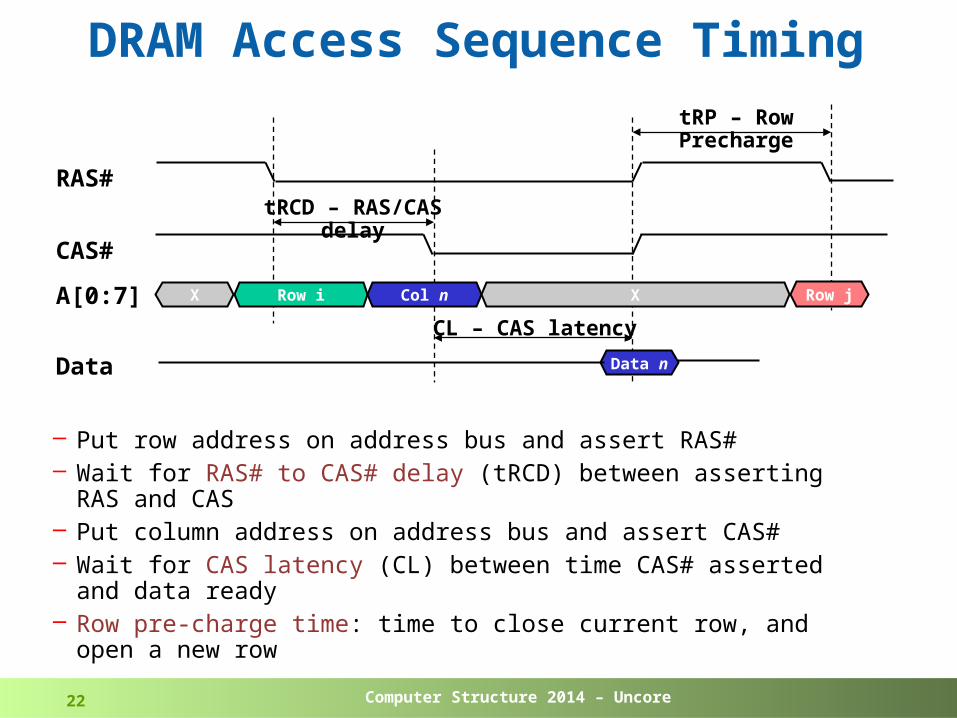
DRAM Access Sequence Timing
– Put row address on address bus and assert RAS#– Wait for RAS# to CAS# delay (tRCD) between asserting RAS and CAS– Put column address on address bus and assert CAS# – Wait for CAS latency (CL) between time CAS# asserted and data ready– Row pre-charge time: time to close current row, and open a new row
tRCD – RAS/CAS delay
tRP – Row Precharge
RAS#
Data
A[0:7]
CAS#
Data n
Row i Col n Row jX
CL – CAS latency
X
Computer Structure 2014 – Uncore23
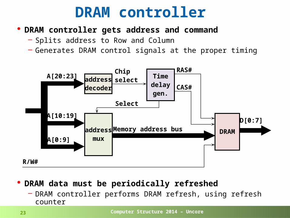
DRAM controller · DRAM controller gets address and command
– Splits address to Row and Column– Generates DRAM control signals at the proper timing
· DRAM data must be periodically refreshed– DRAM controller performs DRAM refresh, using refresh counter
DRAM
addressdecoder
Timedelaygen.
addressmux
RAS#
CAS#
R/W#
A[20:23]
A[10:19]
A[0:9]
Memory address busD[0:7]
Select
Chipselect
Computer Structure 2014 – Uncore24
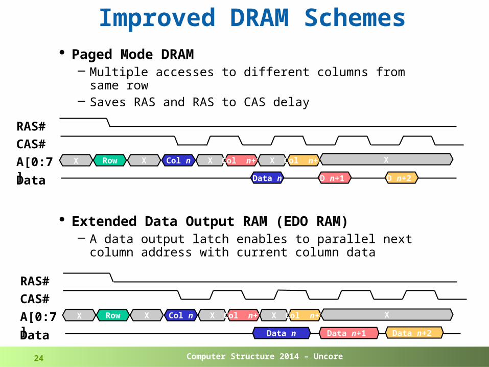
· Paged Mode DRAM– Multiple accesses to different columns from same row– Saves RAS and RAS to CAS delay
· Extended Data Output RAM (EDO RAM)– A data output latch enables to parallel next column address with
current column data
Improved DRAM Schemes
RAS#
Data
A[0:7]
CAS#
Data n D n+1
Row X Col n X Col n+1 X Col n+2 X
D n+2
X
RAS#
Data
A[0:7]
CAS#
Data n Data n+1
Row X Col n X Col n+1 X Col n+2 X
Data n+2
X
Computer Structure 2014 – Uncore25
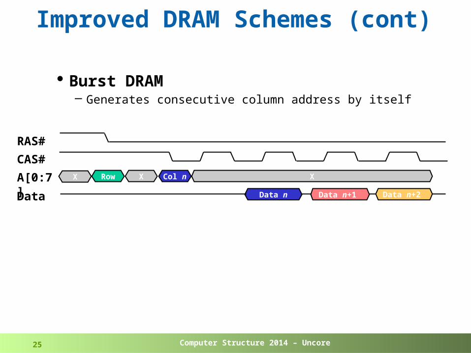
· Burst DRAM– Generates consecutive column address by itself
Improved DRAM Schemes (cont)
RAS#
Data
A[0:7]
CAS#
Data n Data n+1
Row X Col n X
Data n+2
X
Computer Structure 2014 – Uncore26
Synchronous DRAM – SDRAM· All signals are referenced to an external clock (100MHz-200MHz)
– Makes timing more precise with other system devices
· 4 banks – multiple pages open simultaneously (one per bank)
· Command driven functionality instead of signal driven– ACTIVE: selects both the bank and the row to be activated
ACTIVE to a new bank can be issued while accessing current bank– READ/WRITE: select column
· Burst oriented read and write accesses– Successive column locations accessed in the given row – Burst length is programmable: 1, 2, 4, 8, and full-page
May end full-page burst by BURST TERMINATE to get arbitrary burst length
· A user programmable Mode Register – CAS latency, burst length, burst type
· Auto pre-charge: may close row at last read/write in burst
· Auto refresh: internal counters generate refresh address
Computer Structure 2014 – Uncore27
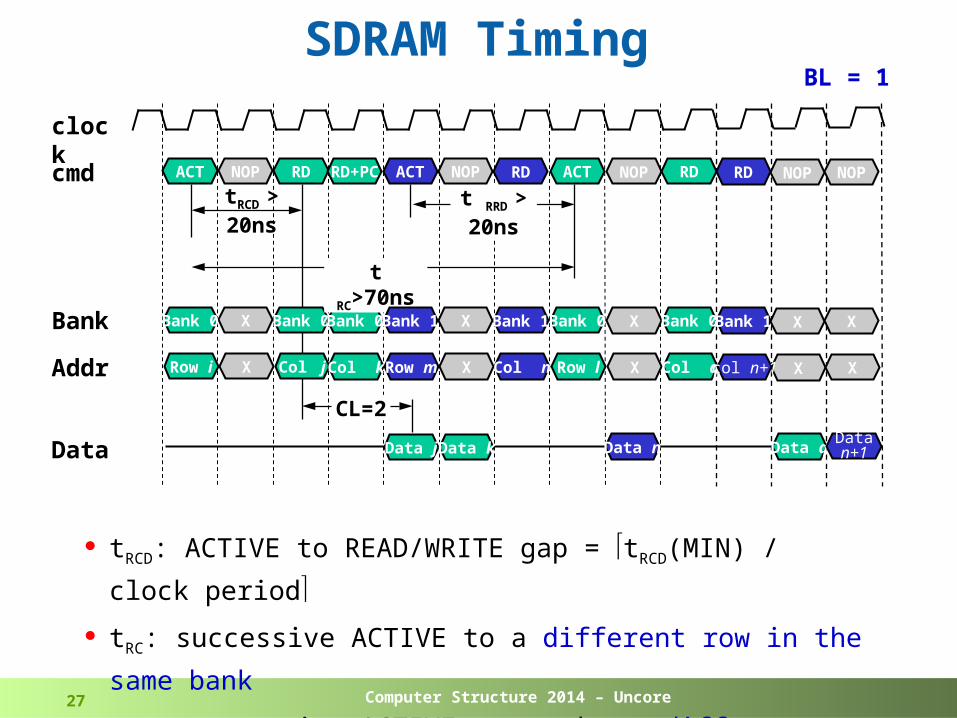
SDRAM Timing
· tRCD: ACTIVE to READ/WRITE gap = tRCD(MIN) / clock period
· tRC: successive ACTIVE to a different row in the same bank
· tRRD: successive ACTIVE commands to different banks
clock
cmd
Bank
Data
Addr
NOP
X
Data j Data k
ACT
Bank 0
Row i X
RD
Bank 0
Col j
tRCD >20ns
RD+PC
Bank 0
Col k
ACT
Bank 0
Row l
t RC>70ns
ACT
Bank 1
Row m
t RRD >20ns
CL=2
NOP
X
X
NOP
X
X
RD
Bank 0
Col q
RD
Bank 1
Col n
NOP
X
X
NOP
X
X
Data n Data q
BL = 1
RD
Bank 1
col n+1
Datan+1
Computer Structure 2014 – Uncore28
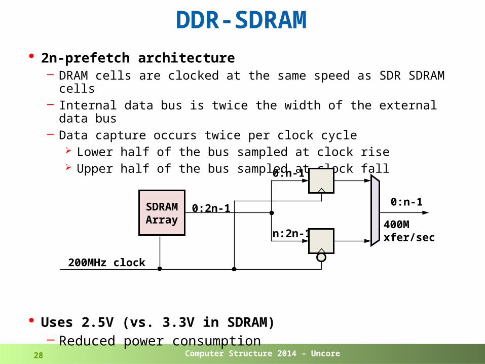
DDR-SDRAM· 2n-prefetch architecture
– DRAM cells are clocked at the same speed as SDR SDRAM cells– Internal data bus is twice the width of the external data bus– Data capture occurs twice per clock cycle
Lower half of the bus sampled at clock rise Upper half of the bus sampled at clock fall
· Uses 2.5V (vs. 3.3V in SDRAM) – Reduced power consumption
n:2n-1
0:n-1
0:n-1
200MHz clock
0:2n-1SDRAMArray 400M
xfer/sec
Computer Structure 2014 – Uncore29
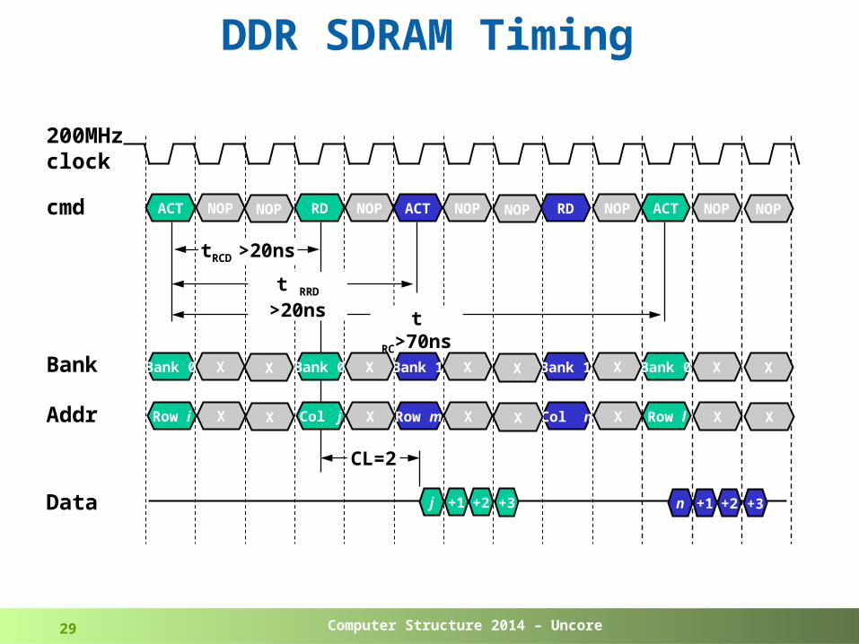
DDR SDRAM Timing
200MHzclock
cmd
Bank
Data
Addr
NOP
X
ACT
Bank 0
Row i X
RD
Bank 0
Col j
tRCD >20ns
ACT
Bank 0
Row l
t RC>70ns
ACT
Bank 1
Row m
t RRD >20ns
CL=2
NOP
X
X
NOP
X
X
NOP
X
X
RD
Bank 1
Col n
NOP
X
X
NOP
X
X
NOP
X
X
NOP
X
X
j +1 +2 +3 n +1 +2 +3
Computer Structure 2014 – Uncore30
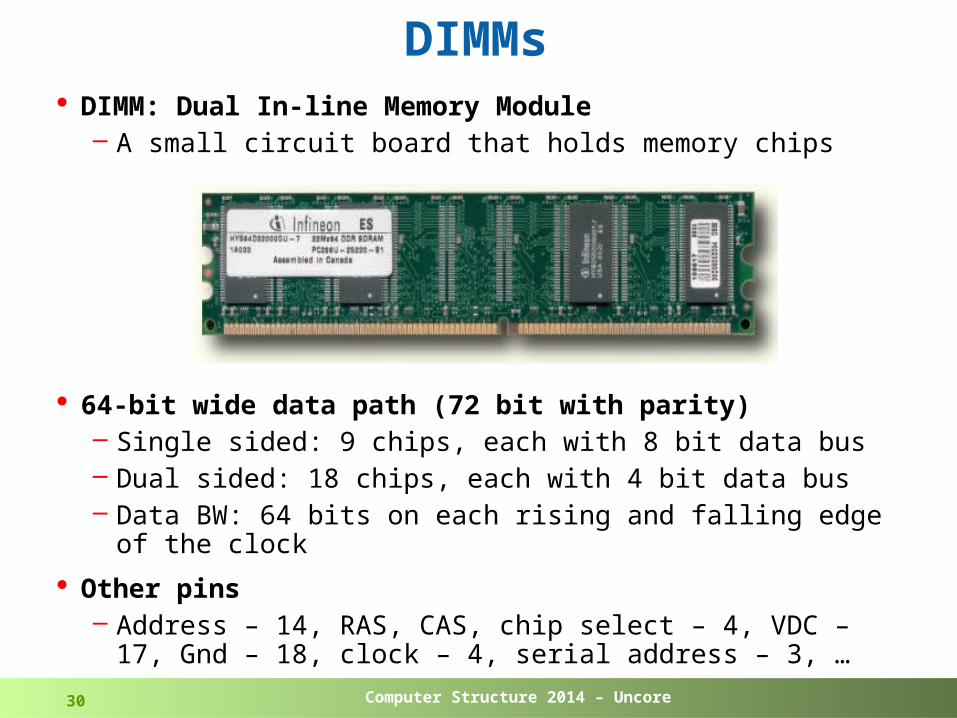
DIMMs· DIMM: Dual In-line Memory Module
– A small circuit board that holds memory chips
· 64-bit wide data path (72 bit with parity)– Single sided: 9 chips, each with 8 bit data bus – Dual sided: 18 chips, each with 4 bit data bus– Data BW: 64 bits on each rising and falling edge of the clock
· Other pins– Address – 14, RAS, CAS, chip select – 4, VDC – 17, Gnd – 18,
clock – 4, serial address – 3, …
Computer Structure 2014 – Uncore31
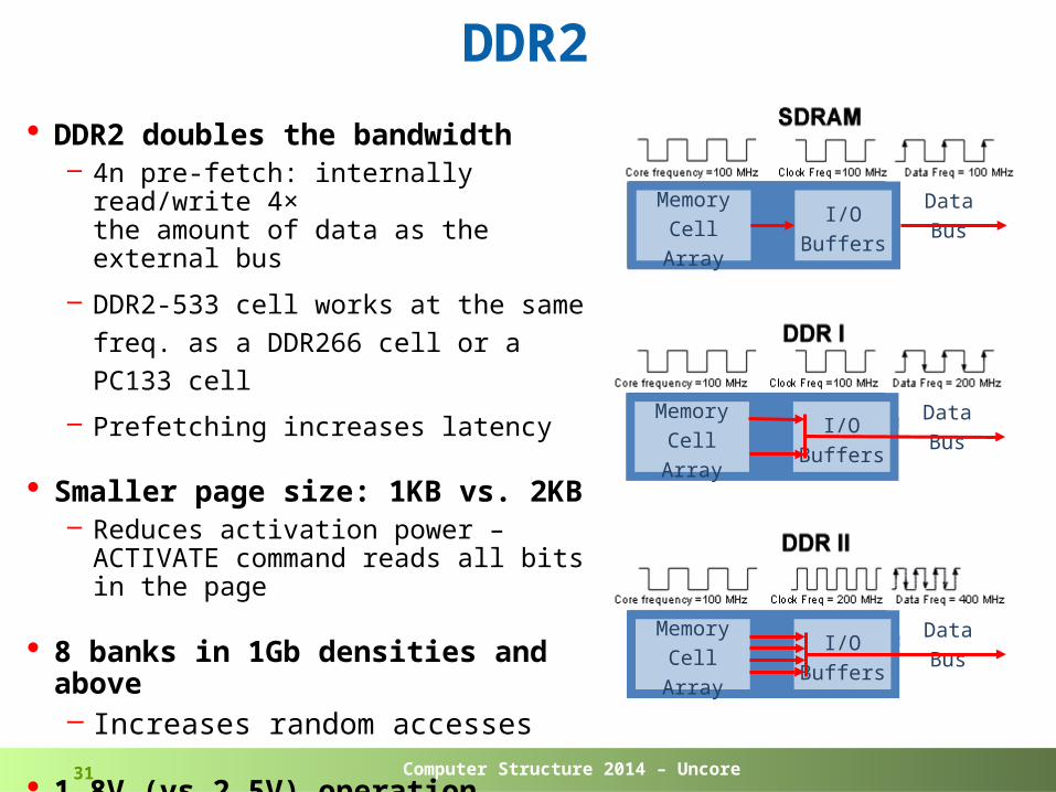
DDR2
· DDR2 doubles the bandwidth – 4n pre-fetch: internally read/write 4×
the amount of data as the external bus
– DDR2-533 cell works at the same freq. as
a DDR266 cell or a PC133 cell
– Prefetching increases latency
· Smaller page size: 1KB vs. 2KB– Reduces activation power – ACTIVATE
command reads all bits in the page
· 8 banks in 1Gb densities and above– Increases random accesses
· 1.8V (vs 2.5V) operation voltage– Significantly lower power
Memory
Cell Array
I/O
BuffersData Bus
Memory
Cell Array
I/O
BuffersData Bus
Memory
Cell Array
I/O
BuffersData Bus
Computer Structure 2014 – Uncore32
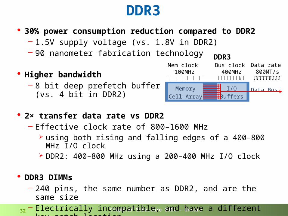
DDR3· 30% power consumption reduction compared to DDR2
– 1.5V supply voltage (vs. 1.8V in DDR2)– 90 nanometer fabrication technology
· Higher bandwidth– 8 bit deep prefetch buffer
(vs. 4 bit in DDR2)
· 2× transfer data rate vs DDR2– Effective clock rate of 800–1600 MHz
using both rising and falling edges of a 400–800 MHz I/O clock DDR2: 400–800 MHz using a 200–400 MHz I/O clock
· DDR3 DIMMs – 240 pins, the same number as DDR2, and are the same size– Electrically incompatible, and have a different key notch location
Memory Cell
Array
I/O
BuffersData Bus
Mem clock 100MHz
Bus clock 400MHz
Data rate 800MT/s
DDR3
Computer Structure 2014 – Uncore33
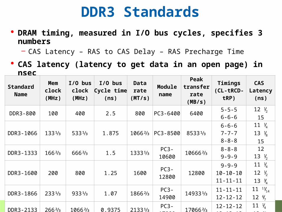
DDR3 Standards· DRAM timing, measured in I/O bus cycles, specifies 3 numbers
– CAS Latency – RAS to CAS Delay – RAS Precharge Time
· CAS latency (latency to get data in an open page) in nsec– CAS Latency × I/O bus cycle time
Standard Name
Mem clock(MHz)
I/O bus clock(MHz)
I/O busCycle time
(ns)
Data rate(MT/s)
Module name
Peak transfer
rate (MB/s)
Timings(CL-tRCD-
tRP)
CAS Latency
(ns)
DDR3-800 100 400 2.5 800 PC3-6400 64005-5-56-6-6
12 1⁄215
DDR3-1066 133⅓ 533⅓ 1.875 1066⅔ PC3-8500 8533⅓6-6-67-7-78-8-8
11 1⁄413 1⁄815
DDR3-1333 166⅔ 666⅔ 1.5 1333⅓ PC3-10600 10666⅔8-8-89-9-9
1213 1⁄2
DDR3-1600 200 800 1.25 1600 PC3-12800 128009-9-9
10-10-1011-11-11
11 1⁄412 1⁄213 3⁄4
DDR3-1866 233⅓ 933⅓ 1.07 1866⅔ PC3-14900 14933⅓11-11-1112-12-12
11 11⁄14
12 6⁄7
DDR3-2133 266⅔ 1066⅔ 0.9375 2133⅓ PC3-17000 17066⅔12-12-1213-13-13
11 1⁄4 12 3⁄16
Computer Structure 2014 – Uncore34
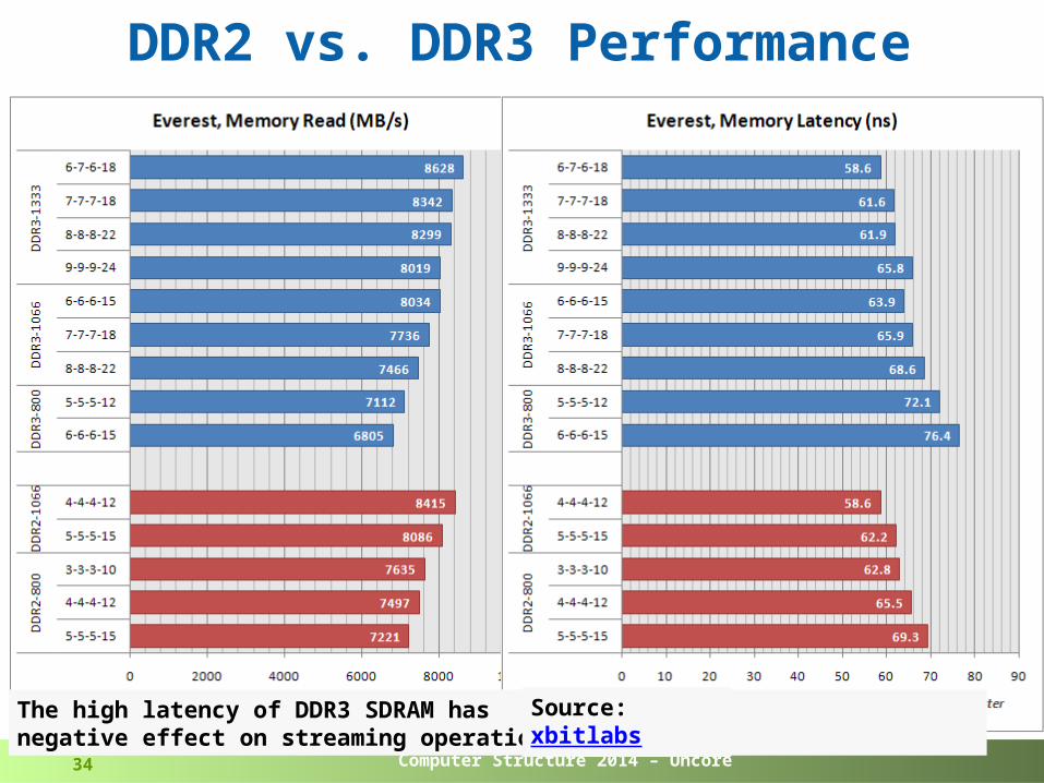
DDR2 vs. DDR3 Performance
The high latency of DDR3 SDRAM has negative effect on streaming operations
Source: xbitlabs
Computer Structure 2014 – Uncore35
How to get the most of Memory ?
· For best performance– Populate both channels with equal amounts of memory
Preferably the exact same types of DIMMs– Use highest supported speed DRAM, with the best DRAM timings
· Each DIMM supports 4 open pages simultaneously– The more open pages, the more random access– It is better to have more DIMMs: n DIMMs 4n open pages – Dual sided DIMMs may have separate CS of each side
Support 8 open pages Dual sided DIMMs may also have a common CS
Computer Structure 2014 – Uncore36
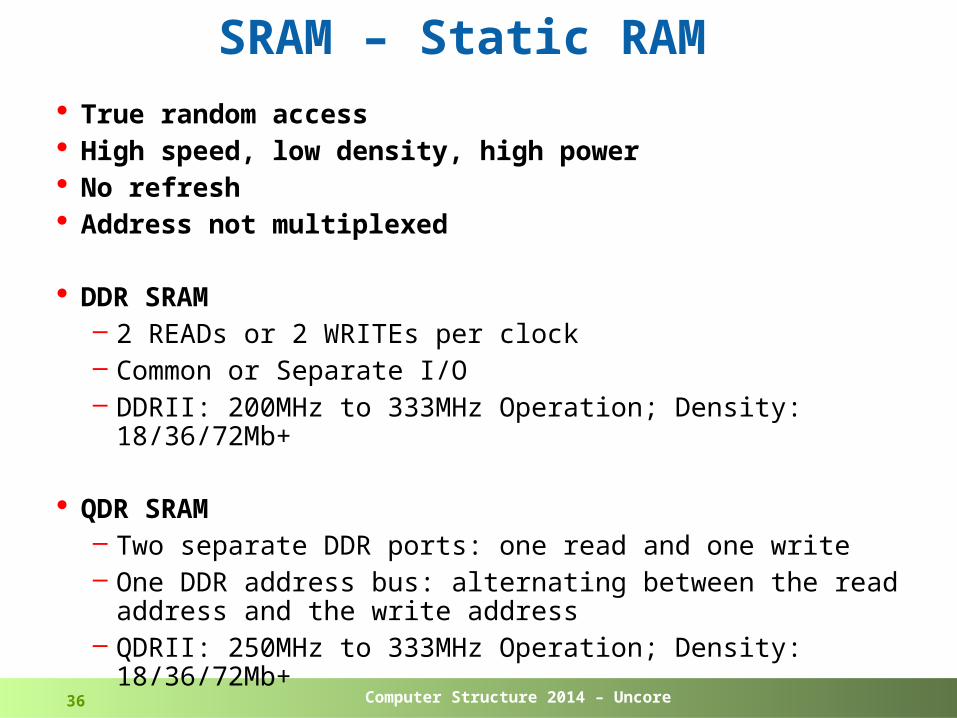
SRAM – Static RAM · True random access· High speed, low density, high power· No refresh· Address not multiplexed
· DDR SRAM– 2 READs or 2 WRITEs per clock– Common or Separate I/O– DDRII: 200MHz to 333MHz Operation; Density: 18/36/72Mb+
· QDR SRAM– Two separate DDR ports: one read and one write– One DDR address bus: alternating between the read address and
the write address– QDRII: 250MHz to 333MHz Operation; Density: 18/36/72Mb+
Computer Structure 2014 – Uncore37
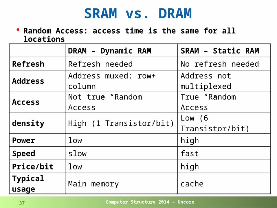
SRAM vs. DRAM· Random Access: access time is the same for all locations
DRAM – Dynamic RAM SRAM – Static RAM
Refresh Refresh needed No refresh needed
Address Address muxed: row+ column
Address not multiplexed
Access Not true “Random Access” True “Random Access”
density High (1 Transistor/bit) Low (6 Transistor/bit)
Power low high
Speed slow fast
Price/bit low high
Typical usage Main memory cache
Computer Structure 2014 – Uncore38
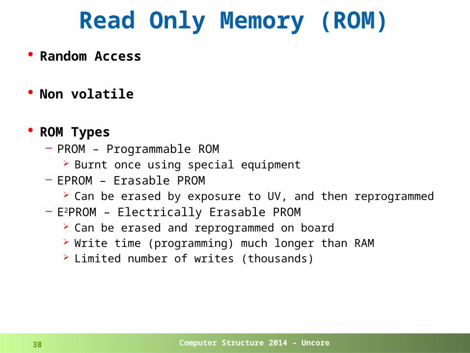
Read Only Memory (ROM)· Random Access
· Non volatile
· ROM Types– PROM – Programmable ROM
Burnt once using special equipment– EPROM – Erasable PROM
Can be erased by exposure to UV, and then reprogrammed– E2PROM – Electrically Erasable PROM
Can be erased and reprogrammed on board Write time (programming) much longer than RAM Limited number of writes (thousands)