
Computer Modeling of Amorphous and Microcrystalline...
88
�������� �� �������� ��� ��������� ������� ������� �� � ��� ���� ����������� ________________________________________________________________________________ ��������� �������� �� ��������� � ���������������� ������������� ����� ������ �� �� ���� ����� ����� ������� ��
Transcript of Computer Modeling of Amorphous and Microcrystalline...

________________________________________________________________________________

Computer Modeling of Amorphous and Microcrystalline Silicon based
Solar Cells
F.A. RubinelliINTEC, Universidad Nacional del
Litoral, Güemes 3450, 3000, Santa Fe, Argentina


Solar Cell ModelingComputer Codes
• True computer modeling solves:
• Poisson’s Equation.• Continuity Equation for Electrons free electricity.• Continuity Equations for Holes.
• First comprehensive computer modeling:• G.A.Swartz, RCA (1982), I.Chen and S.Lee (1982).• T.Ikegaki et all (1985), M.Hack and M.Shur (1985)..• Commercial computer codes:• Medici – TMA company; Atlas – SILVACO company.
Broad range of crystalline semiconductor devices: poly-Si, a-Si TFT and solar cells; 1-D and 2-D codes.Models describing a-Si are relatively simple.

Academic Computer Codes
• AMPS - PennState University – USA (S.Fonash, P.McElheny, J.Arch) (D-AMPS)
• ASPIN - Ljubljana University – Slovenia (Smole, Furlan, Topic, Vukadinovik)
• ASA – Delft University of Technology – Netherlands (Zeeman, Tao, Willeman)
• SCAPS – University of Gen – Belgium, (Burgelman et al.)• P1CD – Sandia Labs.- UNSW, Australia• ADEPT - Purdue University, USA, (Jeff Gray et al.)• Forschungzentrum Jülich (Germany) – Germany, (Stiebig at al.)• Others: ASCA (New UnIv. Lisbon), Chaterjee (INDIA), Misiakos
(Florida USA), Mittiga (La Sapienza, ROMA), Bruns (BERLIN)

Differences in the academic computer codes
• Choice of independent variables: Ψ, EFN, EFP or Ψ, n, p.• Numerical solution techniques: Newton-Raphson, Gummel.• Description of the DOS distribution: Tails and Gaussians.• R-G statistics of localized states; SRH, amphoteric DB.• Contact treatment: generic, ohmic.• Special features: defect pool model, tunnel-recombination junctions,
etc.• Optical models: Interference, scattering.• Friendly interface: AMPS, ASA, ASPIN (no D-AMPS).• 1-D modeling is well suited for a-Si solar cells on flat substrates.• 2-D modeling might be needed on: textured substrates in high efficient
a-Si solar cells (spatial variations in device structure) or in spatially non-homogenous µc-Si devices.

D-AMPSAMPS core (Penn State Univ. USA) + New Developments (INTEC, Argentina)
3 unknown or independent state variables:1 - the electrostatic potential Ψ(x)2 - the electron quasi-Fermi level EFN(x)3 - the hole quasi-Fermi level EFP(x)
Numerical technique:
Finite difference discretizationNewton Raphson formalismTrial functions of Scharletter Gummel (J at i-1/2 i+1/2)
i-1i
I+1vv
v
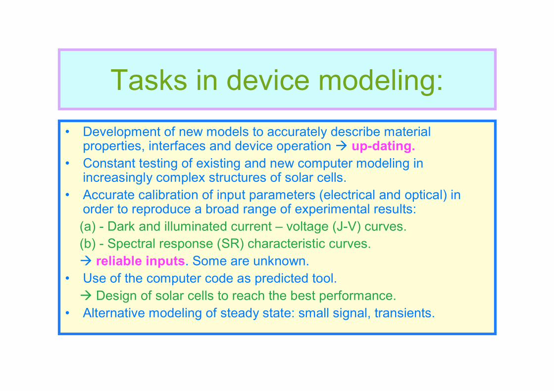
Tasks in device modeling:• Development of new models to accurately describe material
properties, interfaces and device operation up-dating.• Constant testing of existing and new computer modeling in
increasingly complex structures of solar cells.• Accurate calibration of input parameters (electrical and optical) in
order to reproduce a broad range of experimental results:(a) - Dark and illuminated current – voltage (J-V) curves.(b) - Spectral response (SR) characteristic curves.
reliable inputs. Some are unknown.• Use of the computer code as predicted tool.
Design of solar cells to reach the best performance.• Alternative modeling of steady state: small signal, transients.

Advantages of computer modeling
• Examine the influence of internal parameters that can not be experimentally determined.
• Ponder the impact on the solar cell performance of small changes in device configuration.
• Optimal design of the solar cell structure.• Understanding the physic controlling the electrical
transport of interesting experimental results. • It is becoming increasingly cheaper.

Drawbacks of computer modeling
• Too many input parameters?? to be discussed.• Analytical modeling some parameters are ignored or results are
assumed to be independent of these input values.• Some input parameters are not well known (cross sections,
mobilities). We have to work within the range published in the literature.
• Very time consuming task:programming + fitting
• Difficulties found in matching output curves of some devices.example: SR under forward bias.
• Structures of solar cells are becoming increasingly complex.

c-Si N(E) cm-3 eV-1 ~1019cm-3 Mobility gap ~1012cm-3 Valence Band Energy (eV) Conduction band a-Si:H Mobility gap Valence Band Dangling Bonds Conduction band 1020cm-3 1015cm-3 1020cm-3 Energy (eV)
a-Si:H and c-SiDB density: 1015 - 1016 / 1012 cm-3.Mobilities: 2-20/ 480-1500 cm2eV-1sec-1
Gap: 1.80-1.72eV / 1.12eVAbsorption coefficient: one order higher in a-Si:Hin the visible range.
D- D0 D+
Silicio Cristalino Silicio Amorfo Hidrogenado
Enlace covalente
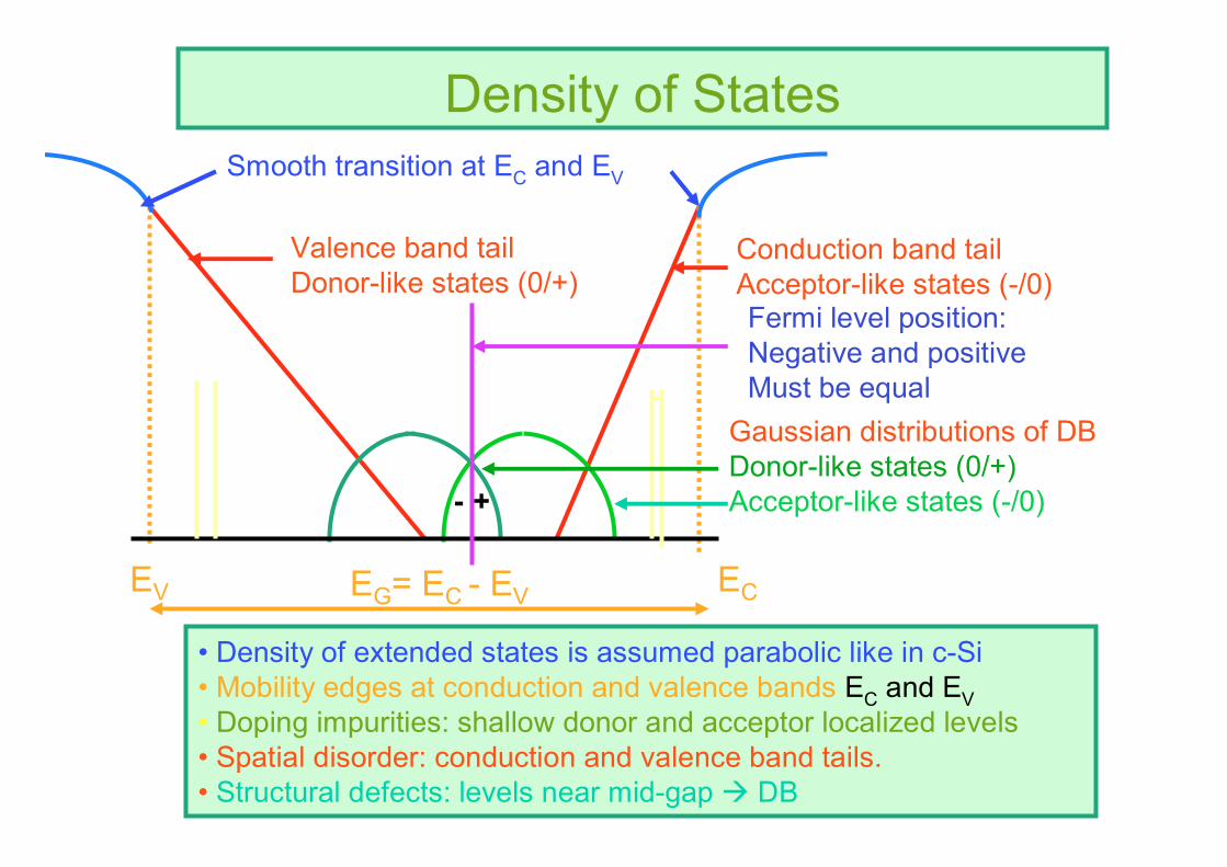
Density of States
• Density of extended states is assumed parabolic like in c-Si• Mobility edges at conduction and valence bands EC and EV• Doping impurities: shallow donor and acceptor localized levels• Spatial disorder: conduction and valence band tails.• Structural defects: levels near mid-gap DB
EV ECEG= EC - EV
Smooth transition at EC and EV
Fermi level position:Negative and positiveMust be equal
Valence band tailDonor-like states (0/+)
Conduction band tailAcceptor-like states (-/0)
Gaussian distributions of DB Donor-like states (0/+)Acceptor-like states (-/0)+-

Transport mechanisms
• Conventional scattering: extended state transport described by carrier concentrations and mobilities
• Multiple trapping: electrons and holes in extended states move by drift-diffusion, they are captured by tail states, remain immobile forsome time, and are re-emitted back into extended states.
described also by concentration of carriers and mobilities• Hopping: involves tunnel between localized states inside the mobility gapThermally activated and negligible at room temperature
ConventionalScattering
Multiple Trapping
Hopping RT
SRH
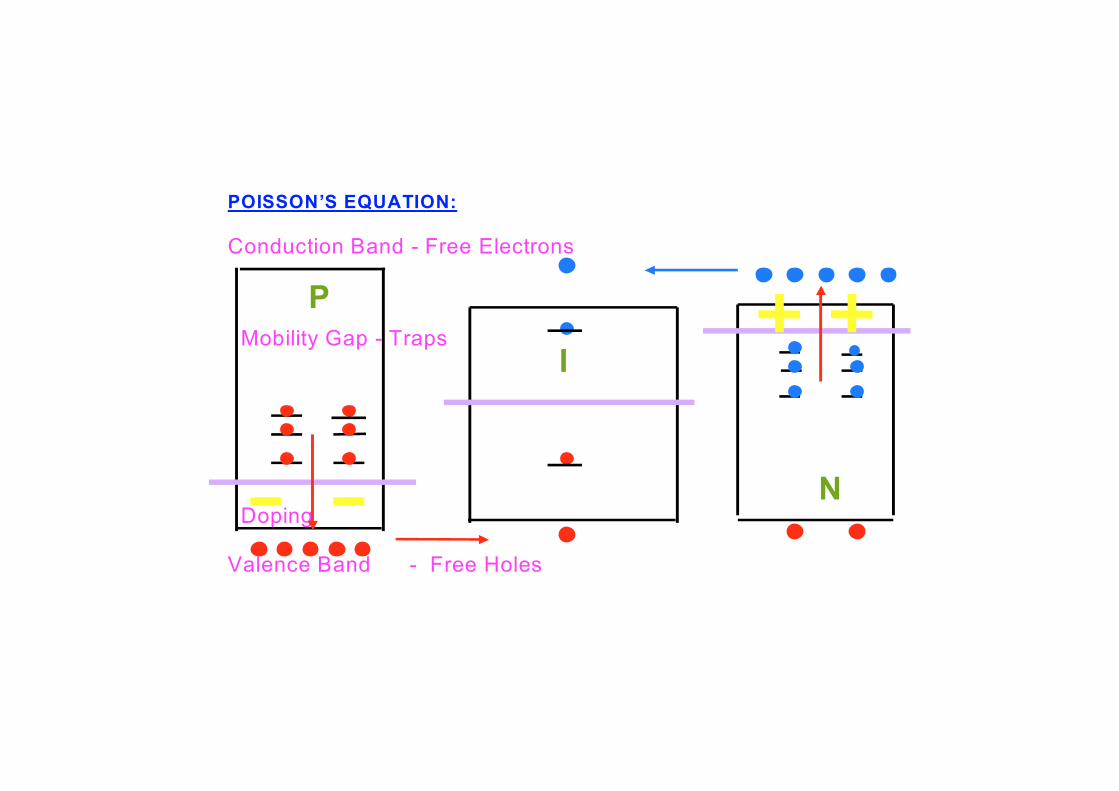
POISSON’S EQUATION:
Conduction Band - Free Electrons
Mobility Gap - Traps
Doping
Valence Band - Free Holes
P
I
N

Poisson’s EquationEquilibrium
(x)dx(x)d)(x
dxd ρε =⎟
⎠⎞
⎜⎝⎛ Ψ
ΕP-N
Ε
ψ (x)ρ (x)
P
I
N∫L E(x) dx= C

Poisson’s EquationUnder illumination
Ε (light)

Continuity EquationsElectrical Currents:
(a) - Drift (Holes)
(b) – Diffusion (Holes)
(c) - Effective field: gap, electron affinity, (Electrons) EC
Drift
Diffusion
EC
EV
EFN
EFP
0 =(x)R-(x)Gdx(x)dJ
q1
netoptn
+
− +1q
dJ (x)dx
G (x)-R (x) = 0popt net
dx(x)dE
(x)n(x)q FNnµ+
−q (x)p(x) dE (x)dxpFPµ
Jn(x)=
Jp(x)=
x=0
x=L

Total current
0 =(x)R-(x)Gdx(x)dJ
q1
netoptn
+ J= JN+JP
∫∫ ⋅⋅−⋅⋅++=L
0
L
0pLn0 dxGopt(x)edxRnet(x)eJJJ
Electron back diffusion
Hole back diffusion
Recombinationlosses
Optical currentTotal Current

ΦBL
Front OpticalRegion
Back OpticalRegion
P
I
N
η O
η L
EF
Pin + optical layers

Charge, f, and R (equations)[ ]∫ ⋅−⋅⋅= c
v
E
EdEf(E)1N(E)qρ acceptor∫ ⋅⋅⋅−= c
v
E
EdEf(E)N(E)qρdonor
pn
n
)σp'p()σn'(nσ)p'(nf+++
+=
pn
2i
pnthT )σp'p()σn'(nnpnσσvNR+++
−⋅⋅⋅⋅⋅=
TkEE FT
e1
1f⋅−
+=
TkEE
c
cT
eNn' ⋅−
⋅= TkEE
v
Tv
eNp' ⋅−
⋅=
SRHFD
vTH~ 107cm/s

Boundary Conditions
ΦL
ΦO
JN(0)= SNO[n(0)-nO(0)]
JN(L)= SNL[n(L)-nO(L)]
JP(0)= SPO[p(0)-pO(0)]
JP(L)= SPL[p(L)-pO(L)]
(a) electronic potential Ψ fixed at contacts(b) Currents at contacts are ~ S (Thermionic Emission)
Tunneling
Recombination
Thermionic emission J ~ S S > 105cm/s

Working StrategyMaterial Characterization
1- Dark conductivity
Mobility x Free carrier concentration (µnn or µpp)
Ec
Eact EF Ev
Dark Conductivity vs. temperature ===> Eact
2- Photoconductivity
Light: AM1.5 or Red LightFree carrier concentration lifetime Density of dangling bonds (Do)
Ec
electron trapping EFN recombination EFP hole trapping Ev

Material Characterization
CPM: Constant Photocurrent MethodDBP: Dual Beam Photoconductivity, Others (PDS) Valence Band Tail Slope and Dangling Bond Density (D- and Do)
Subgap Absorptiona-Si:H Mobility gap Valence Band Dangling Bonds Conduction band 1020cm-3 1015cm-3 1020cm-3 Ev D+ Do D- Ec Energy (eV)

Optical characterization of materials
4 - Reflection and Transmission:
I
R T
Material Glass
Absorption coefficients (α) and Refractive Indexes (n)Optical Gap (Tauc Gap) α(hν)n(hν) ~ (hν-EOPT)1/2
Cutoff Wavelength or Photon Energy
EOPT (a-Si:H) = 1.72eV EOPT (c-Si) = 1.12eVEOPT (µc-Si:H) = 1.1ev (I) –2.00eV (D)

5 - Electron Spin Resonance:
Dangling Bond concentration --> Do
6 - Internal Photoemission:
Mobility Gap
SSPGModulated conductivityMinority carrier diffusion lengthConduction Band Tail (Time of Flight)
Y(hν) ~ (hν-ΦOE)2
Other techniques
ΦOE
ΦOH
EG = ΦOE +ΦOH

Inputs – Equilibrium Poisson’s Equation – n,p
(x)dx
(x)d)(xdxd ρε =⎟
⎠⎞
⎜⎝⎛ Ψ
ρ(x)= q[p(x)-n(x) + pT(x) - nT(x) + ND+(x) - NA-(x) ]
Dielectric permittivity ε books
n ~ NC exp(EFN -EC) p ~ NV exp(EV - EFP)EG = EC - EV
EG
p ~ NV
EFN
EFP
EC
EV
n ~ NC
NC :effective conduction density of statesinput (literature, fitting) (cm-3)
NV :effective valence density of statesinput (literature, fitting) (cm-3)
Usually NC= NV (1) (1-3x10²⁰)
EG: mobility gap (eV), (1)input (experiment)

Inputs – Equilibrium Poisson’s Equation - DOS
GDO GAO
ED EA
Conduction band tail (acceptor-like)gD(E)=GDOexp (-E/ED) GDOkT~ NVValence band tail VBT (donor-like)gA(E)=GAOexp (-E/EA) GAOkT~ NC
GDO density of localized states at Ec(cm-3eV-1) input (literature)GAO density of localized states at Ev(cm-3eV-1) input (literature)Usually GDO= GAO (2)
ED: donor tail characteristic energy (eV) input (experiment) (2)EA: acceptor tail characteristic energy (eV) input (literature, fitting) (3)
EV EC

Inputs – Equilibrium Poisson’s Equation - DOS
SAG
gAG(E)= exp
gDG(E)= exp
N2 S
AG
AGπ( )
⎥⎥⎦
⎤
⎢⎢⎣
⎡− 2
AG
2AG
2SE -E
N2 S
DG
DGπ( )
⎥⎥⎦
⎤
⎢⎢⎣
⎡− 2
DG
2DG
2SE -E
NDG
SDG
EDG
NAG
EAG
NDG, NAG total number of states enclosed in Gaussians (cm-3) inputs (4) NDG = NAGEDG, EAG, peak energies (eV)
input We have to reproduce the experimental i-layer activation energy EAG =EDG+ UU: correlation energy (literature)SDG, SAG: standard deviations (eV)
inputs (4) Usually SAG= SDG
Usually•NAG1= NDG1•NAG2= NDG2•NAG3= NDG3•NDG1= NDG3= 2xNDG2NDB= 5xNDG2
U
ECEV
∆

n-layer ND+ (fully ionized, fix DOS) We have to reproduce the n-layer activation energy EACT(N) (experiment)
Inputs – Equilibrium Poisson’s Equation - DOS
EACT(P)
EACT(N)
p-layer NA- (fully ionized, fix DOS) We have to reproduce the p-layer activation energy EACT(P) (experiment)
ΦBO= EG(P) – EACT(P)ΦBL= EACT(N)Flat band conditions
ΦBO
ΦBL
Ec
Ev
EF

Non – Equilibrium Poisson’s + Continuity Equations
Tail cross sections σNA, σPA,σND, σPDinputs (literature, fitting)
σNA << σPA, and σPD << σND (6) (6)Often but not alwaysσPA= σND and σNA= σPDMid-gap cross sections σNA, σPA, σND, σPD
inputs (literature, fitting)σNA << σPA, and σPD << σND (8) (8)Often but not alwaysσPA= σND and σNA= σPD
Recombination (R) and occupation functions (f)(nT and pT) are functions of the cross sections.
EC
EV
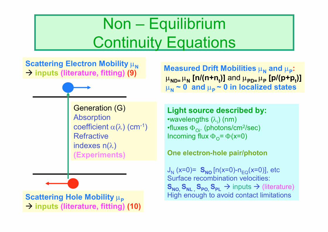
Non – Equilibrium Continuity Equations
Scattering Electron Mobility µNinputs (literature, fitting) (9)
Scattering Hole Mobility µPinputs (literature, fitting) (10)
Generation (G)Absorption coefficient α(λ) (cm-1)Refractive indexes n(λ)(Experiments)
Measured Drift Mobilities µN and µP:µND= µN [n/(n+nt)] and µPD= µP [p/(p+pt)]µN ~ 0 and µP ~ 0 in localized states
Light source described by:•wavelengths (λi) (nm) •fluxes ΦOi. (photons/cm2/sec) Incoming flux ΦO= Φ(x=0)
One electron-hole pair/photon
JN (x=0)= SNO [n(x=0)-nEQ(x=0)], etcSurface recombination velocities: SNO, SNL , SPO, SPL inputs (literature)High enough to avoid contact limitations

Critical parameters:How many?
• a-Si (~1.8eV)
ED and NDG can be carefully measured (DBP, PDS).
EG can be also measured (IPE).EA only impacts on the high forward
dark J-V.σPA, in tails has much less impact on
device outputs that σND.
We have five critical parameters per layer:
µN, µP, σPA (DB), σND (DB).and σND (T).
and 13 non-critical inputs.
• µc-Si (~1.2-1.6eV)
In low gap materials tails do not play a significant role!
We end up with four critical parameters per layer:
µN, µP, σPA, (DB) and σND (DB)
and seven non-critical inputs

Device characterization
-1.0 -0.5 0.0 0.5 1.0 1.5 2.010-8
10-7
10-6
10-5
10-4
10-3
10-2
10-1
100
101
102
103
HIGH FORWARD
LOW FORWARDREVERSE
J (m
A/cm
2 )V (V)
J
V
Dark Current - Voltage Curve
Limited by R(G) ~ ni
2NTσ
ni2 ~ exp(EG/kT)
Limited by SCLC
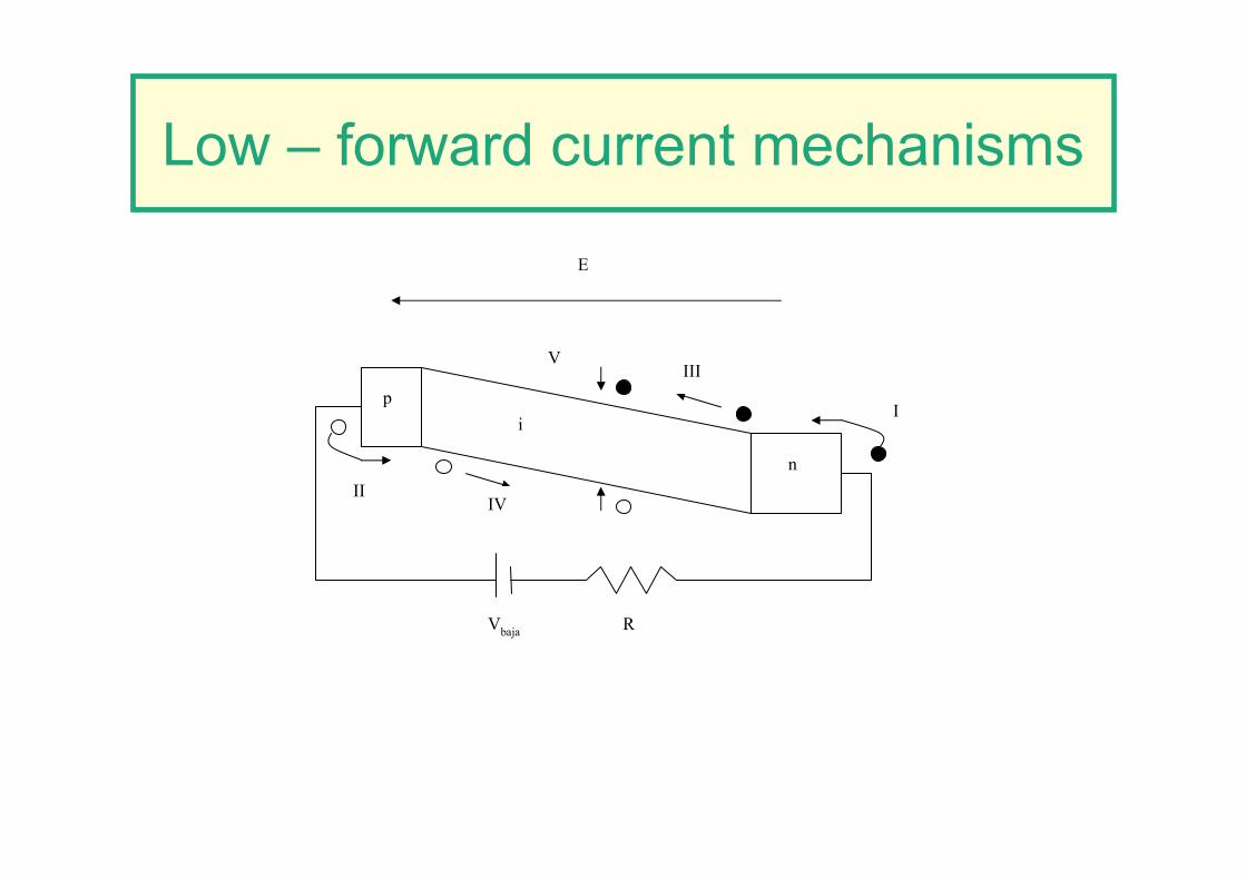
Low – forward current mechanisms
Vbaja R
E
p
n
iI
II
III
IV
V

High – forward current mechanisms
Valta R
E
p
n
i
I
II
III
IV
V
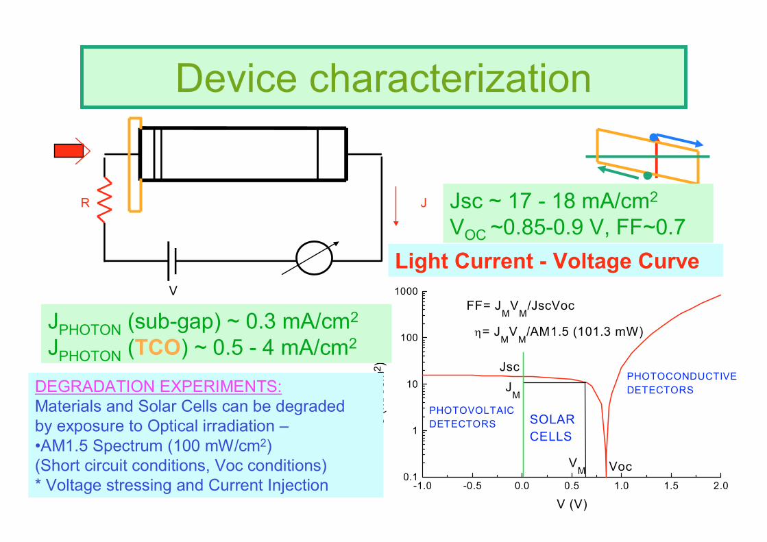
Device characterization
R J
V
-1.0 -0.5 0.0 0.5 1.0 1.5 2.00.1
1
10
100
1000
PHOTOCONDUCTIVEDETECTORS
SOLAR CELLS
PHOTOVOLTAIC DETECTORS
η= JM
VM
/AM1.5 (101.3 mW)
VM
JM
FF= JM
VM
/JscVoc
Voc
JscJ
(mA/
cm2 )
V (V)
Light Current - Voltage Curve
JPHOTON (sub-gap) ~ 0.3 mA/cm2
JPHOTON (TCO) ~ 0.5 - 4 mA/cm2
DEGRADATION EXPERIMENTS:Materials and Solar Cells can be degraded by exposure to Optical irradiation –•AM1.5 Spectrum (100 mW/cm2)(Short circuit conditions, Voc conditions)* Voltage stressing and Current Injection
Jsc ~ 17 - 18 mA/cm2
VOC ~0.85-0.9 V, FF~0.7

Solar Spectrum
0.4 0.5 0.6 0.7 0.8 0.9 1.0 1.10.0
2.0x10¹⁵
4.0x10¹⁵
6.0x10¹⁵
8.0x10¹⁵
1.0x10¹⁶
a-SiC:Hµm-Si
a-Si:H
c-Si
Phot
ons/
cm2 /s
ec
Wavelength (µm)
0.4 0.5 0.6 0.7 0.8 0.9 1.0 1.10.0
0.5
1.0
1.5
2.0
2.5
3.0
3.5
Ener
gy (m
W/c
m2 )
Wavelenght (µm)
η(%) = JMVM/qΦ < 100% Maximum Currents:JPHOTON= 43.25 mA/cm2 (c-Si)JPHOTON= 15.28 mA/cm2 (a-SiC:H)JPHOTON= 22.20 mA/cm (a-Si:H) Experimental Jsc ~ 17 - 18 mA/cm2
Maximum efficiencies:η(%) = 79.7 (c-Si) - 50.5 (a-Si:H) absorbed energyη(%) = 48.4 (c-Si) - 38.2 (a-Si:H) optical gapη(%) = 45.6 (c-Si) – 23.6 (a-Si:H) activation energyHighest experimetal efficiencies ~ 15%
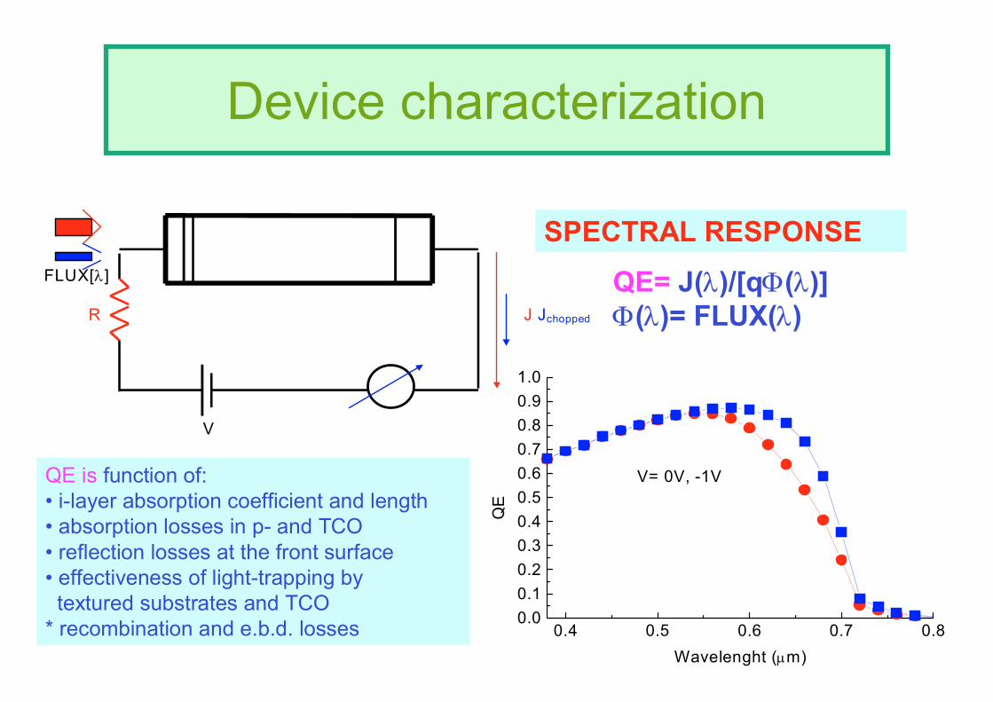
Device characterization
FLUX[λ]
R J Jchopped
V
0.4 0.5 0.6 0.7 0.80.00.10.20.30.40.50.60.70.80.91.0
V= 0V, -1VQ
E
Wavelenght (µm)
SPECTRAL RESPONSE
QE= J(λ)/[qΦ(λ)]Φ(λ)= FLUX(λ)
QE is function of:• i-layer absorption coefficient and length• absorption losses in p- and TCO• reflection losses at the front surface• effectiveness of light-trapping by
textured substrates and TCO* recombination and e.b.d. losses
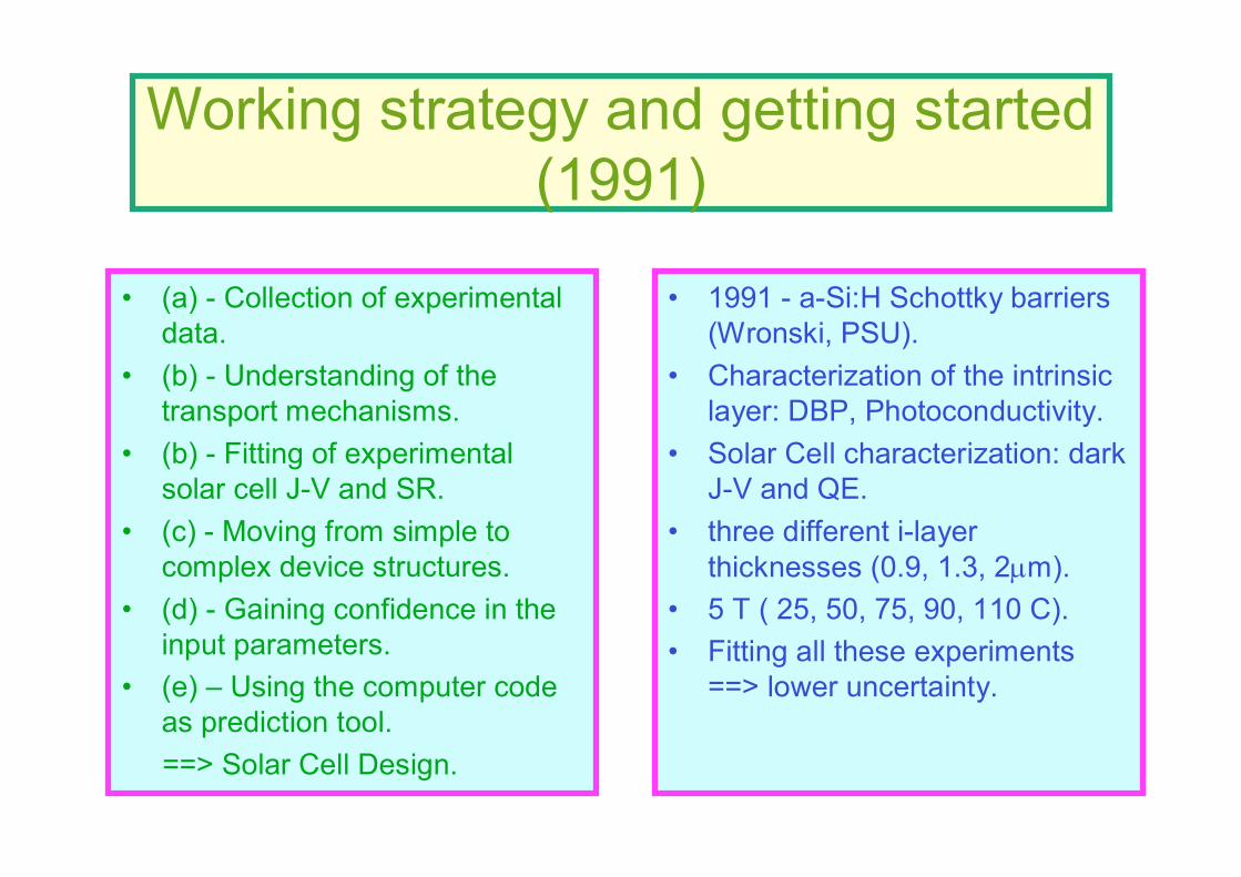
Working strategy and getting started (1991)
• (a) - Collection of experimental data.
• (b) - Understanding of the transport mechanisms.
• (b) - Fitting of experimental solar cell J-V and SR.
• (c) - Moving from simple to complex device structures.
• (d) - Gaining confidence in the input parameters.
• (e) – Using the computer code as prediction tool.==> Solar Cell Design.
• 1991 - a-Si:H Schottky barriers (Wronski, PSU).
• Characterization of the intrinsic layer: DBP, Photoconductivity.
• Solar Cell characterization: dark J-V and QE.
• three different i-layer thicknesses (0.9, 1.3, 2µm).
• 5 T ( 25, 50, 75, 90, 110 C).• Fitting all these experiments
==> lower uncertainty.
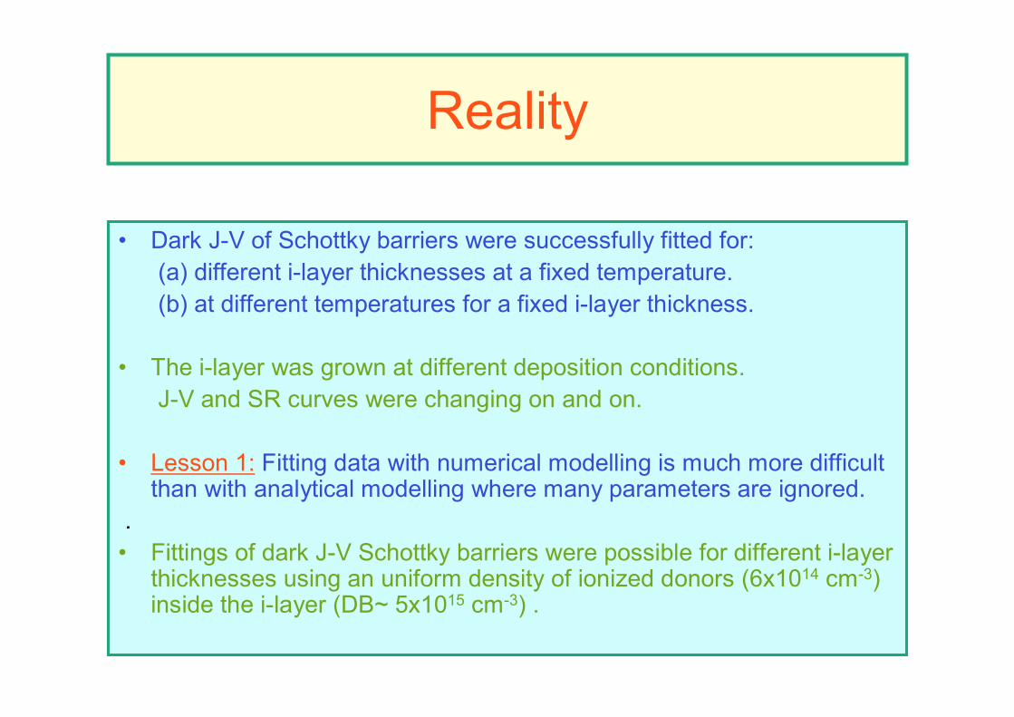
Reality
• Dark J-V of Schottky barriers were successfully fitted for:(a) different i-layer thicknesses at a fixed temperature.(b) at different temperatures for a fixed i-layer thickness.
• The i-layer was grown at different deposition conditions.J-V and SR curves were changing on and on.
• Lesson 1: Fitting data with numerical modelling is much more difficult than with analytical modelling where many parameters are ignored.
.• Fittings of dark J-V Schottky barriers were possible for different i-layer
thicknesses using an uniform density of ionized donors (6x1014 cm-3) inside the i-layer (DB~ 5x1015 cm-3) .

RealityLesson 2: elaborated modelling does not necessarily helps (DOS).
• To fit dark J-V of a-Si p-i-n at different thicknesses we did not need to ionized donors in the i-layer.
• Lesson 3: what is learned in simple devices does not necessarily apply directly to more complex devices.
• Lesson 4: Better quality materials does not imply better solar cells (defect pool model).
• Lesson 5: Physics has to be constantly updated.
• Inverse modelling: fitting of experiments could be automatically achieved by running the computer code commanded by an auxiliary program that minimizes the mean square deviation between data and simulations.

Some important results (1992-1998)
• Basic Device Physics:Why the high forward dark J-V in p-i-n a-Si homojunctions is higher than in m-i-n a-Si Schottky barriers?
• SR > 1 in a-Si based devices:In a-Si based sensors BLUE bias light could give rise toSR >1. The QE peak is function of: bias and monochromatic light intensities, device length, DOS, forward bias voltage..
• a-SiC/c-Si Hybrid Cells - Evidence of Tunneling:Light J-V with good FF can not be explained without invoking tunneling currents flowing through the VB.spike present at the a-SiC/c-Si interface.

Fitting experimentaldark and light J-Vin Schottky barriersand in p-i-n a-Sidevices
Red light sourcewith intensities of9x1015 #/cm2/sec7x1016 #/cm2/sec (S)
1

Transport mechanisms in the dark
p-i-n vs. Schottky
1

Measured QE characteristicsof a Ni/(i)-a-Si/(n)-a-Si Schottkybarrier for three different appliedvoltages: -3, 0, and 0.2V under(a) Dark conditions(b) Red bias light illumination(c) Blue bias light illumination
2
Predicted QE peak fordifferent (i)-layer thicknesses

Red and bluebias light generatemodificationsin the electric field with opposite directions at the front regionof the i-layer
2

The spike at the a-SiC/c-Si interfaces was measured with internal photoemission and it was found to be ∆EV= 0.6eV
Only by including the tunneling path at that VB spike it becomespossible to reproduce high experimental FF with our simulations
3

Modeling refinements: DB are really amphoteric
DB behave as donors and acceptor-like states they are amphotericDB can be represented by two energy levels separated by UD+ (0 electrons), D0 (1 electron) and D- (2 electrons)
donor
acceptor
UED-PEAK
EAM-PEAK
Amphoteric states with energy EAM can be approximated by donor – acceptor pairs with energies ED and EA
σND (σN+) >> σNA (σN
0) (charged >> neutral) σPA (σP
-) >> σPD (σP0) (charged >> neutral)
U > 0 (positive correlation energy)
•EAM-PEAK = ED-PEAK•EA-PEAK = ED-PEAK + UEA-PEAK
EA 0/-ED +/0
0/-EAM +/0U U
amphoteric

0.0 0.2 0.4 0.6 0.8 1.0 1.2 1.4 1.6 1.8 2.010-7
10-6
10-5
10-4
10-3
10-2
10-1
100
101
102
U>0σCH>σ0
ANFOTERICO DONOR-ACEPTOR
T=300 K
J (m
A/c
m2 )
V (V)
Approximation fails when U>0 and σCH≤σ0, or when U<0.
DB approximated by donor-acceptor pairs
• U > 0• σCH >> σ0 CH= Charged 0= Neutral
0.0 0.1 0.2 0.3 0.4 0.5 0.6 0.7 0.8 0.9 1.00
2
4
6
8
10
12
14
16
U>0σ
CH>σ
0
ANFOTERICO DONOR-ACEPTOR
T=300 K
J (m
A/cm
2 )V (V)
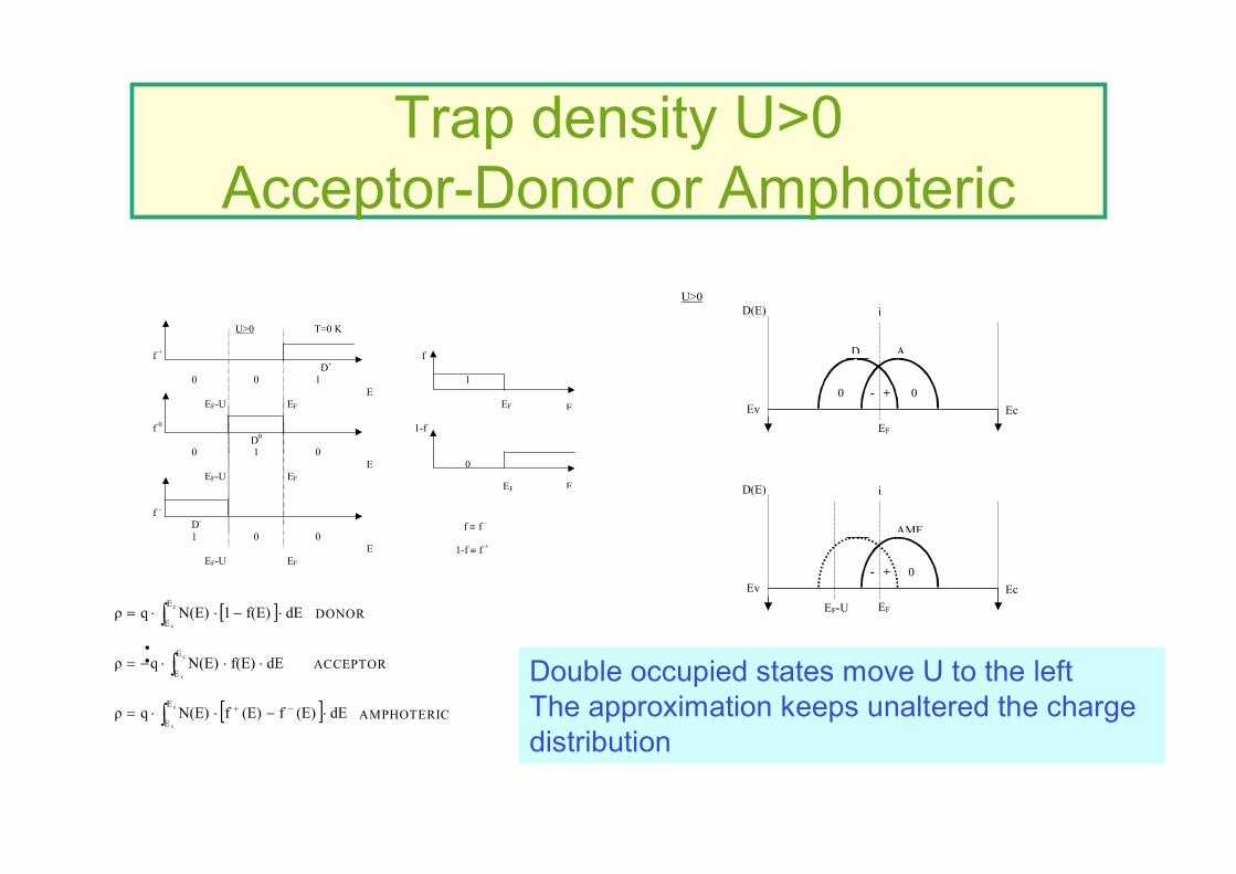
Trap density U>0 Acceptor-Donor or Amphoteric
f + f D+ 0 0 1 1 E EF-U EF EF f 0 1-f D0 0 1 0 E 0 EF-U EF f -
D- 1 0 0 E EF-U EF
U>0 T=0 K
E
EEF
f ≡ f -
1-f ≡ f +
U>0
D(E) 0 - + 0 D(E) - + 0
Ev EcEF
D A
i
Ev EcEF
AMF
i
EF-U
: [ ]∫ ⋅−⋅⋅= c
v
E
EdEf(E)1N(E)qρ DONOR
∫ ⋅⋅⋅−=c
v
E
EdEf(E)N(E)qρ ACCEPTOR
[ ]∫ ⋅−⋅⋅= −+c
v
E
EdE(E)f(E)fN(E)qρ AMPHOTERIC
Double occupied states move U to the leftThe approximation keeps unaltered the charge distribution

U>0 and σp- = σp
0 (σn+ = σn
0, )amphoteric state (-) only can trap holes
D(E) σp
0, σn+ 0 - σp
-, σn0
h h
Ev EcEF
D A
n D(E) n D- σp
-, σp0 : no aporta
h
Ev EcEF
D-
n

Defect Pool ModelSuccessful in describing the defect density in doped and un-doped a-Si
Accounts for the origin of DB WB ↔ DB conversion H mediates in the reaction
WB ↔ 2DB (i=0)Si – H + WB ↔ (DB + Si-H) + DB (i=1)2(Si – H) + WB ↔ (Si-H-H-Si) + 2DB (2)
Energy distribution of WB VB tail state distribution gD(E)=GDOexp(-E/ED)· P(E): distribution of available defect sites: Gaussian distribution
EDP: peak position or defect pool center σDP: defect pool standard deviation
( )⎥⎦
⎤⎢⎣
⎡ −−⎥⎦
⎤⎢⎣
⎡≡ 2
2
2exp
21)(
DP
DP
DP
EEEPσπσ
0.0 0.3 0.6 0.9 1.2 1.5 1.81016
1017
1018
1019
1020
1021
H
µDEF
EDP,σDP
2DBWB
EcEv
DO
S (c
m-3.e
V-1)
Energy (eV)

Defect Pool
0.0 0.1 0.2 0.3 0.4 0.51015
1016
1017
1018
1019
buffers
Intrinsic Layer np
UDM DPM
Den
sity
of D
B (c
m-3)
X (µm)
DB density results from minimizing the free energy G of the system WB + DB + Si-H + HChemical Defect PotentialµD= < e > - kTse (+ H term) ~ EF (D+ p-a-Si)~ E (D0 i-a-Si) ~ 2E – EF +U (D- n-a-Si) Two (one) algorithms of Powell and Deane (Schuum) No evidences of defect pool in µc-Si
DB density becomes function of the EF positionTEQ: freezing or equilibration temperature D(E) at T < TEQ = D(E) at TEQ (frozen at TEQ)EDP coincides with D+ peak = EF + ∆/2σDP ∆= 2ρσDP
2/ED – U ~0.44eVOut New Same
NG1, NG2, NG3 TEQ ED EG1, EG2 , EG3 EDP GDO SG1= SG2= SG3 H σN
0 , σP- , σN
+, σP0
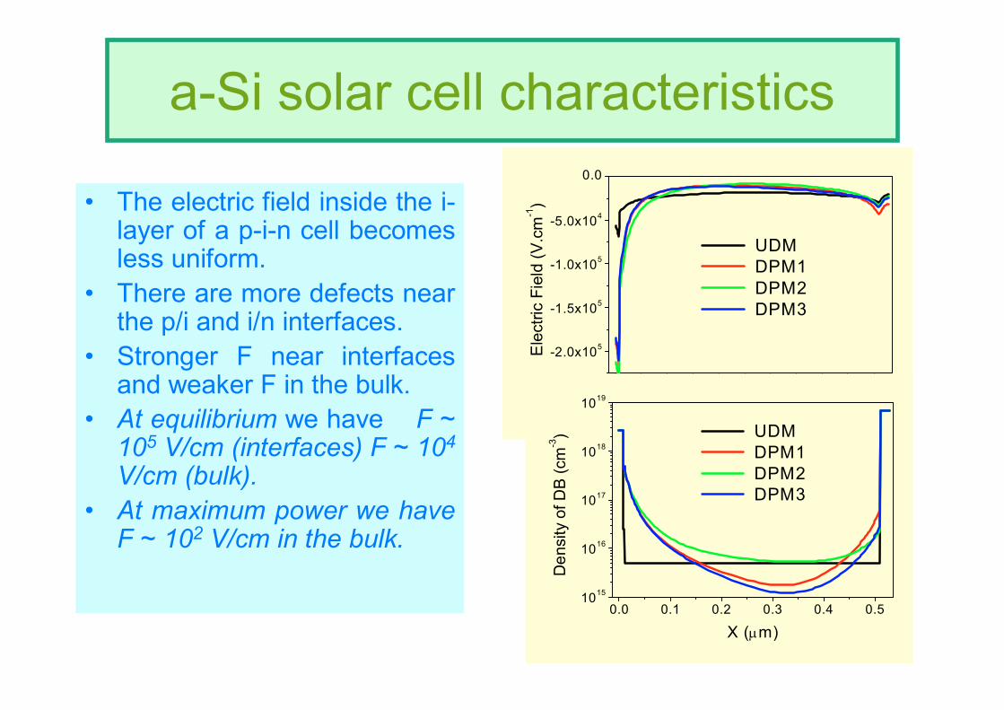
a-Si solar cell characteristics
• The electric field inside the i-layer of a p-i-n cell becomes less uniform.
• There are more defects near the p/i and i/n interfaces.
• Stronger F near interfaces and weaker F in the bulk.
• At equilibrium we have F ~ 105 V/cm (interfaces) F ~ 104
V/cm (bulk).• At maximum power we have
F ~ 102 V/cm in the bulk.
0.0 0.1 0.2 0.3 0.4 0.5
-2.0x10⁵
-1.5x10⁵
-1.0x10⁵
-5.0x10⁴
0.0
UDM DPM1 DPM2 DPM3
Ele
ctric
Fie
ld (V
.cm
-1)
X (µm)
0.0 0.1 0.2 0.3 0.4 0.51015
1016
1017
1018
1019
UDM DPM1 DPM2 DPM3
Den
sity
of D
B (c
m-3)
X (µm)
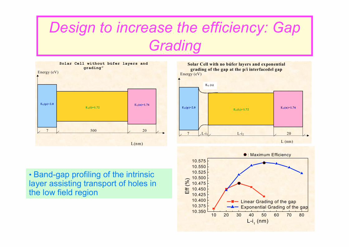
Design to increase the efficiency: Gap Grading
Solar Cell without búfer layers and grading”
Energy (eV)
7 500 20
L(nm)
EG(i)=1.72
EG(n)=1.76
EG(p)=2.0
Solar Cell with no búfer layers and exponential grading of the gap at the p/i interfacedel gap
Energy (eV) 7 L-i1 L-i2 20
L (nm)
EG(i2)=1.72
EG(n)=1.76
EG(p)=2.0
EG (x)
10 20 30 40 50 60 70 8010.35010.37510.40010.42510.45010.47510.50010.52510.55010.575
: Maximum Efficiency
Linear Grading of the gap Exponential Grading of the gap
Eff
(%)
L-i1 (nm)
• Band-gap profiling of the intrinsic layer assisting transport of holes in the low field region

Doping and Gap GradingSolar Cell with no búfer layers and exponential
grading of the gap at the p/i interfacedel gap Energy (eV) 7 L-i1 L-i2 20
L (nm)
EG(i2)=1.72
EG(n)=1.76
EG(p)=2.0
EG (x)
• Field redistribution using low-level of impurity doping
•They will also introduce more defects
0 10 20 30 40 50 60 70 8010.62510.65010.67510.70010.72510.75010.77510.80010.82510.85010.87510.90010.925
Linear Grading lineal of borom exponencial Grading of borom
Eff
(%)
L-i1 (nm)
0 10 20 30 40 5010.55010.57510.60010.62510.65010.67510.70010.72510.75010.77510.800
Exponential Grading of all the electrical parameters at the p/i interface
Eff
(%)
L-i1 (nm)

0 10 20 30 40 50 60 70 807.007.257.507.758.008.258.508.759.009.259.509.75
10.0010.2510.5010.75
Gap Grading B Grading Gap and B Grading Grading all the electrical parameters
: Maximum Efficiency
Eff (
%)
L-i1 (nm)
0 10 20 30 40 5010.55010.57510.60010.62510.65010.67510.70010.72510.75010.77510.800
Exponential Grading of all the electrical parameters at the p/i interface
Eff
(%)
L-i1 (nm)
• EG, χ, EDP, σDP, NA, ED, EA, µn, µp, Nc, Nv, σCH,0.
• Effmáx=10.77%.• Highest impact: ED.
Exponential Grading of all electrical parameters
i/n interface
• Gap grading increases Eff.• P grading decreases Eff.
UDM: p/i interface
• Grading NDB decrese of Eff.• Recommend removal of buffer
layers to increase the Eff contradicts experimental findings.
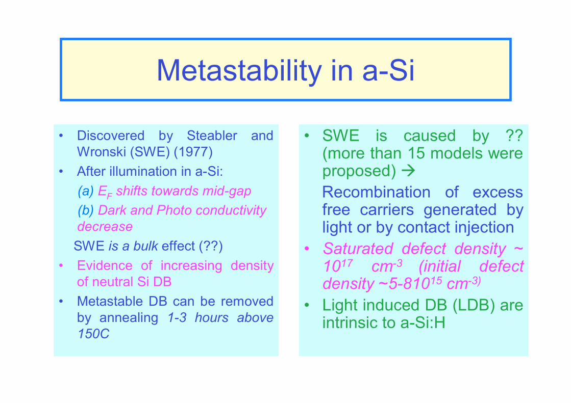
Metastability in a-Si
• Discovered by Steabler and Wronski (SWE) (1977)
• After illumination in a-Si:(a) EF shifts towards mid-gap(b) Dark and Photo conductivity decreaseSWE is a bulk effect (??)
• Evidence of increasing density of neutral Si DB
• Metastable DB can be removed by annealing 1-3 hours above 150C
• SWE is caused by ?? (more than 15 models were proposed) Recombination of excess free carriers generated by light or by contact injection
• Saturated defect density ~ 1017 cm-3 (initial defect density ~5-81015 cm-3)
• Light induced DB (LDB) are intrinsic to a-Si:H

Metastabilityin a-Si Solar Cells
• (a) - Largest changes occur in FF.• (b) - Changes in JSC and and VOC are small.• (c) – Thicker cells degrade deeper.• (d) – Cells with high impurity concentration (> 1018cm-3) in the intrinsic layer
degrade deeper than cells with highly pure intrinsic layers.• (e) – Cells operating at high T (60-90C) stabilize at higher efficiencies than
cells operating a 300K.• (f) – Exposure to high (low) intensity illumination causes deeper (reduced)
degradation.• (g)– Cells with intrinsic layers made with highly hydrogen-diluted silane
stabilize at a higher η.• (h) No correlation between films and cell stability. Defect pool model
influences results on cells. Fermi level change with position in cells.

Metastabilityin a-Si Solar Cells
• Rate of degradation under 1 sun is(a) – high during first tens of hours(b) – decreases over time (c) – stabilizes after hundreds of hs(d) – initial efficiency can be recovered by annealing(150C for several hours)
• Degradation not caused by(1) – diffusion of ions or dopants(2) – electrical migration
• LDB introduce extra recombination and trapping
• SWE modifies the electric field inside the device
0.0 0.1 0.2 0.3 0.4 0.5 0.6 0.7 0.8 0.902468
101214161820
Experimental Curve DPM3
J (m
A/c
m2 )
Voltage (V)
0.0 0.1 0.2 0.3 0.4 0.5 0.6 0.7 0.802468
1012141618
Experimental Curve DPM4
J (m
A/c
m2 )
Voltage (V)
0.0 0.1 0.2 0.3 0.4 0.51016
1017
1018
1019
Stabilized State
UDM DPM4 DPM1 DPM2
Den
sity
of D
B (c
m-3)
X (µm)0.0 0.1 0.2 0.3 0.4 0.5
1015
1016
1017
1018
1019Initial and Stabilized States
DPM3 DPM4
Den
sity
of D
B (c
m-3)
X (µm)
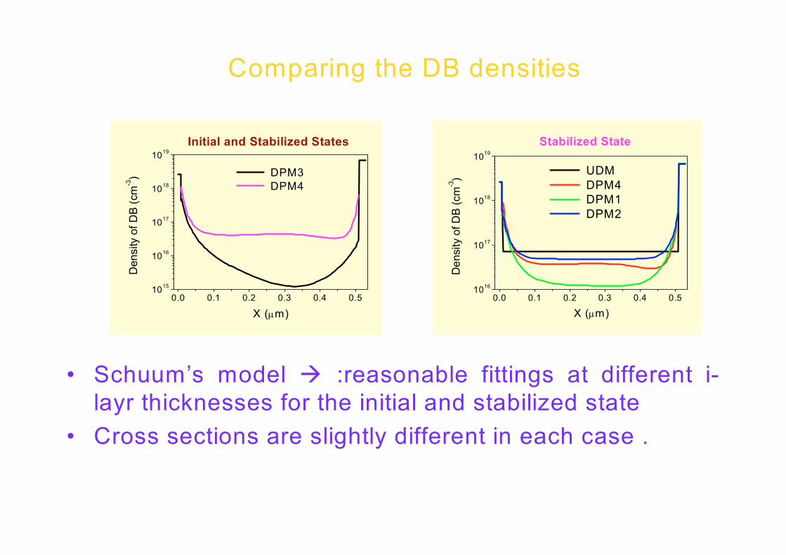
Comparing the DB densities
• Schuum’s model :reasonable fittings at different i-layr thicknesses for the initial and stabilized state
• Cross sections are slightly different in each case .
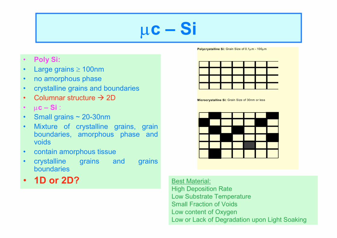
µc – Si• Poly Si: • Large grains ≥ 100nm • no amorphous phase • crystalline grains and boundaries • Columnar structure 2D• µc – Si :• Small grains ~ 20-30nm• Mixture of crystalline grains, grain
boundaries, amorphous phase and voids
• contain amorphous tissue • crystalline grains and grains
boundaries
• 1D or 2D?
Polycrystalline Si: Grain Size of 0.1µm - 100µm Microcrystalline Si: Grain Size of 30nm or less
Best Material:High Deposition Rate Low Substrate TemperatureSmall Fraction of VoidsLow content of OxygenLow or Lack of Degradation upon Light Soaking

Comparing a-Si and µc-Si
a-Si:H• Frequency deposition:
13.5 MHz - 200MHz• Low temperature deposition TS
~ 420 - 520K• Deposition rate (PECVD) ~ 0.3
nm/sec at 13.5 MHz 5 times higher at VHF-GD
• Staebler Wronski EffectDegradation of its electrical properties under illuminationDark conductivity increasesPhotoconductivity decreases
µc-Si:H• Same frequency deposition: but
prepared at higher H dilutions and RF power
• Low substrate temperature TS < 500C (High TS poly-Si)
• Advantages over a-Si: • (a) - lower SWE• (b) - higher light absorption in
the infrared region• Drawbacks: • (a) - thick absorbing layers at
low deposition rates• (b) anomalous incorporation of
impurities (mainly O)

Device Quality MaterialIntrinsic a-Si and µc-Si
• Dark conductivity < 10-10 Ω-1 cm-1
• AM1.5 conductivity > 10-8 Ω-1 cm-1
• Activation Energy ~ 0.8eV• Mobility Gap < 1.8eV (1.72eV)• Density of Dangling Bonds
≤ 1016 cm-3 (opto-electrical) and 8x1015 cm-3 (ESR)
• µτELECTRONS ~ 10-6 cm2/V • µτHOLES ~ 10-8 cm2/V• Minority LD ~ 100-200nm• Absorption Coefficient
≥ 3.5 x 104 cm-1 at 600nm and 5 x 105 cm-1 at 400nm
• Dark conductivity < 10-7 Ω-1 cm-1
• AM15 conductivity > 10-5 Ω-1 cm-1
• Activation Energy ~ 0.53-0.57eV• Mobility Gap: 1.2 –1 6 eV• Density of Dangling Bonds
≤ 1016 cm-3 (ESR)• µτHOLES ~ 10-7 cm2/V • Minority LD > 500nm• Crystalline volume fraction (Raman)
> 90%• Lower values are acceptable in µ c-
Si cells.

Light absorption of a-Si and µc-Si
0.0 0.5 1.0 1.5 2.0 2.5-1.5-1.2-0.9-0.6-0.30.00.30.60.91.21.5
BOTTOMµc-Si
TOPa-Si
Band
s (e
V)
X(µm)
a-Si/µc-Si Tandem
Main breakthroughs in solar cells over the past 25 years (MRS –2004)
• (1) Textured transparent contacts for light trapping • (2) a-Si deposited with hydrogen dilution for greater stability • (3) a-SiC and µc-Si doped layers for higher Voc and better blue
response• (4) TCO/silver and TCO/aluminum rear contact for enhanced
reflectivity • (5) Multi-gap, multi-junction devices for optimum utilization of the solar
spectrum• (6) µc-Si intrinsic layers for improved red-response and stability• (7) Band gap tailoring and engineering of device structure for optimum
performance (a-SiGe and a-Si)

Front electrode Textured contacts – Light trapping
• TCO (pin) SnO2:F, ZnO:Al, relatively thick ~ 600nm and textured. (nip). ITO (In2O3:Sn) 70-80 nm
• Requirements: Highly transparent lo light and highly conductive • Ability to scatter light Haze ratio (TDIFFUSE/TTOTAL) (TTOTAL = TDIFFUSE + TSPECULAR usually taken in air) • Optimum Haze Ratio ~ 6-15%.
• Should provides an antireflection layer.• Sheet resistance is high.
Metal grid to reduce series resistance.And to keep FF reasonably high.
=φ ΣφiTDIFFUSE
TSPECULAR
φ
rms
TCO
p
i
air (Glass)

Rough and Flat TCO Hydrogen diluted a-Si
0 .0 0 .1 0 .2 0 .3 0 .4 0 .5-1 .5-1 .2-0 .9-0 .6-0 .30 .00 .30 .60 .91 .21 .5
Band
s (e
V)
X (µm )0.0 0.2 0.4 0.6 0.8 1.0
0
3
6
9
12
15
18
Non diluted a-Si Diluted a-Si Non diluted a-Si Flat Interfaces
J (m
A/cm
2 )
V (V)
• Rough TCO increases Jsc by ~ 1mA/cm2
• a-Si gap is increased from 1.72 to 1.82eVVoc increases ~ 0.1V= ∆EG

a-SiC and µc-Si doped layers
a-Si (1.72eV)a-SiC (2.0eV)µc-Si (1.2eV)
0.3 0.4 0.5 0.6 0.7 0.80.00.10.20.30.40.50.60.70.80.9
Experimental Curve DPM3S
R
Wavelength (µm)
P

Device Quality MaterialDoped a-Si and µc-Si
0.0 0.1 0.2 0.3 0.4 0.5 0.6-1.5-1.2-0.9-0.6-0.30.00.30.60.91.21.5
(n)-a-Si (1.72 eV)E
ACT= 0.25eV
(i)-a-Si (1.72eV)E
ACT= 0.77eV
(p)-a-SiC (2 eV)EACT= 0.47eV
EG= 1.72 eVBan
ds (e
V)
X (µm)•p-type (20nm thick) a-Si•Conductivity > 10-7 Ω-1 cm-1
•Activation Energy < 0.5 eV•Band Gap (Tauc) > 2.0 eV•Absorption Coefficient at 400nm < 3x105 cm-1
•Absorption Coefficient at 600nm < 104 cm-1
•n-type (15nm thick)•Conductivity > 10-4 Ω-1 cm-1
•Activation Energy < 0.3 eV•Band Gap (Tauc) > 1.75 eV
•p-type (20nm thick) µc-Si•Conductivity 2.6X10⁻² Ω-1 cm-1
•Activation Energy ~ 0.059eV
•n-type (15nm thick)•Conductivity 2.5 Ω-1 cm-1
•Activation Energy ~ 0.026eV
0.0 0.1 0.2 0.3 0.4 0.5 0.6-1.5-1.2-0.9-0.6-0.30.00.30.60.91.21.5
(n)-µc-Si (1.12 eV)EACT= 0.026eV
(i)-a-Si (1.72eV)EACT= 0.77eV
(p)-µm-Si (1.2 eV)EACT= 0.059eV
EG= 1.72 eVBand
s (e
V)
X (µm)
• .

(i)layer built-in potentials µc-Si vs. non µc-Si doped layers
0.0 0.1 0.2 0.3 0.4 0.5-1.5-1.2-0.9-0.6-0.30.00.30.60.91.21.5
n-layera-Si (single)µc-Si (tandem)p-layer
a-SiC (single)µc-Si (tandem)same thickness
(i)a-Si layerBlue --> singlered-green --> tandem(same thickness)
Band
s in
Equ
libriu
m (e
V)
X (µm)
0.00 0.01 0.02 0.03 0.04 0.05 0.06-0.9-0.6-0.30.00.30.60.91.21.5
a-SiC EG= 2.0eV
µc-SiEG= 1.2eV
p-layer
Band
s in
Equ
libriu
m (e
V)
X (µm)
0.45 0.46 0.47 0.48 0.49 0.50 0.51 0.52-1.5
-1.2
-0.9
-0.6
-0.3
0.0
0.3
0.6 EG=1.72eV
EG=1.2eVn-layer
Ban
ds in
Equ
libriu
m (e
V)
X ( m)
Similar built-in potentialscan be obtained in the(absorbing) i-layers with µc-Si or with a-Si based doped layers
µc-Si doped layers provide high built-in potentials

p(µc-Si)/(i)a-Si/(n)a-Si

TCO/silver and TCO/aluminum rear contact for enhanced reflectivity
0
5
10
15
20
25
30
0 0.1 0.2 0.3 0.4 0.5 0.6voltage (V)
curre
nt d
ensi
ty (m
A/cm
2 )
FitA luminiumZnO
• Silane/ hydrogen dilution: 0.95 (5%)• Substrate configuration: SS: cells were deposited onto SS
•n-type µc-Si: doped with P, 0.05µm, PECVD.•intrinsic µc-Si:H: 3µm, HWCVD technique•p-type µc-Si: doped with B, 0.025µm, PECVD•ITO: Indium Tin Oxide, •Au (gridlines).
• Al or/and zinc oxide (ZnO) at the back contact • Back reflector is included in simulations •Jsc increases ~4mA/cm2, resulting in an efficiency enhancement from 5.1% to 6.2% • Extra light absorbed at back region of the i-layer reflected off the back contact• The enhancement of Jsc is more significant in solar cells with thinner i-layers
ITOp
i
nss

µc-Si (i)-layersSingle p-i-n solar cells
Order improves in the growth direction at any given dilution Problems in solar cells with intrinsic layers in excess to 1µm
FF decays with thickness deterioration of the material quality with increasing thickness; Voc decays with thickness grain size is increasing
AM1.5 illumination a-Si alloy top cell on SS (4 different hydrogen dilutions) Jsc (mA/cm2) Voc (V) FF Pmax(mW/cm2)Near optimum 10.04 1.018 0.732 7.48 Optimum 9.88 1.028 0.761 7.73 On-the-edge 9.82 0.624 0.426 2.61 Over-the-edge 8.95 0.459 0.562 2.31 (MRS 2004, (R. S.Guha))
Thickness (nm) Jsc (mA/cm 2) Voc (V ) FF P ma x(mW /cm 2) 335 9 .45 0.47 0.651 2.89 470 10.98 0.466 0.672 3.44 720 12.99 0.439 0.640 3.65 1040 14.8 0.434 0.621 3.99 1395 16.51 0.414 0.578 3.95 1980 17.87 0.393 0.510 3.58 (M RS 2004, (R . S.G uha))

µc-Si (i)-layersSingle p-i-n solar cells
Beginning with a very high H dilution to reduce the incubation layerDecreasing the hydrogen dilution with time deposition conditions are kept near the edgeSmall and uniform grain size throughout the whole film thickness1D Modeling is applicable !! (we are lucky)
Thickness (nm) Jsc (mA/cm2) Voc (V) FF Eff (%) Baseline 22.58 0.495 0.603 6.74 20% ticker No profiling
21.48 0.482 0.632 6.54
20% ticker with profiling
25.15 0.502 0.663 8.37
(MRS 2004, (R. S.Guha))

Multi-junction devices for optimum utilization of the solar spectrum
VFB
35 mA/cm2
0.52V1.12-0.08-0.09=0.95V
0.339 x 10¹⁷
58.3 mA/cm2
25 mA/cm2
0.53V1.2-0.059-0.026= 1.11V
0.996 x 10¹⁷
37.1 mA/cm2
17 mA/cm2
0.9V1.72-0.33- 0.25=1.14V
1.328 x 10¹⁷
21.2 mA/cm2
JscVoc
Flat Band Voltage (VFB)
Total fluxes (#/cm2/sec)
Single a-Si (17x0.9) 15.3mWSingle µc-Si: (25x0.53) 13.2mWSingle c-Si: (35x0.52) 18.2 mWa-Si/ µc-Si Tandem: [(25/2)x(0.9+0.53)= 17.9mWa-Si/ µc-Si/c-Si Triple: [(35/3)x(0.9+0.53+0.52)= 22.7mW
0.3 0.4 0.5 0.6 0.7 0.8 0.9 1.0 1.10.0
2.0x10¹⁵
4.0x10¹⁵
6.0x10¹⁵
8.0x10¹⁵
1.0x10¹⁶
c-Si1.12eV
µc-Si1.25eV
a-Si1.72eV
Flux
(pho
tons
/cm
2 /sec
)
W avelength (µm )
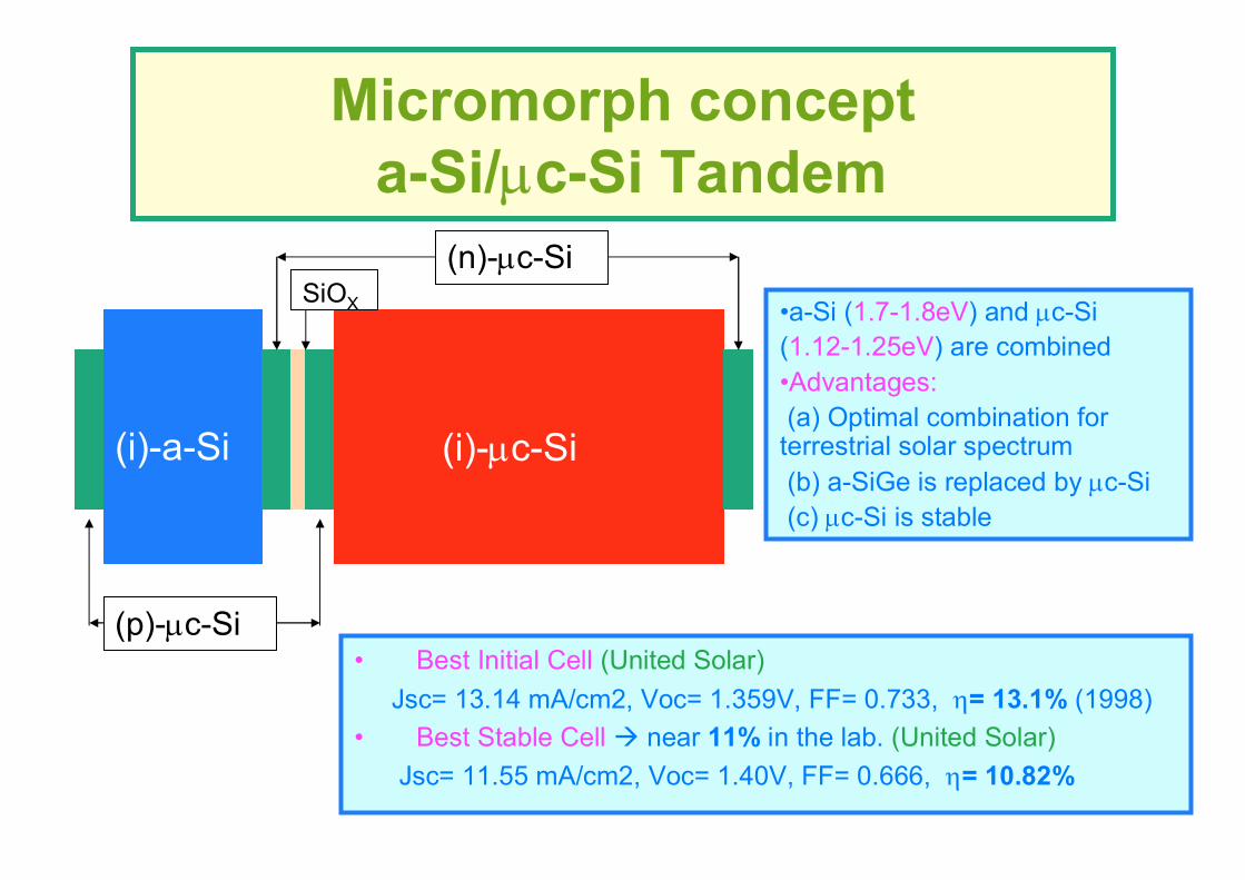
Micromorph concepta-Si/µc-Si Tandem
• Best Initial Cell (United Solar)Jsc= 13.14 mA/cm2, Voc= 1.359V, FF= 0.733, η= 13.1% (1998)
• Best Stable Cell near 11% in the lab. (United Solar)Jsc= 11.55 mA/cm2, Voc= 1.40V, FF= 0.666, η= 10.82%
(i)-a-Si (i)-µc-Si
(p)-µc-Si
(n)-µc-SiSiOX •a-Si (1.7-1.8eV) and µc-Si
(1.12-1.25eV) are combined•Advantages:(a) Optimal combination for
terrestrial solar spectrum(b) a-SiGe is replaced by µc-Si(c) µc-Si is stable

Tandem and TRJ Bands
0.0 0.1 0.2 0.3 0.4 0.5 0.6 0.7-1.6
-1.2
-0.8
-0.4
0.0
0.4
0.8
1.2
1.6TRJ
BOTTOMTOPBand
Dia
gram
(eV)
Position (µm)
0.13 0.14 0.15 0.16 0.17 0.18 0.19 0.20-1.6
-1.2
-0.8
-0.4
0.0
0.4
0.8
1.2
1.6
(i)µc-Si (p)µc-Si(n)µc-SiBan
d D
iagr
am (e
V)
Position (µm)

TRJ µc-Si doped layers provide efficient recombination junctions for photo-carriers
0.50 0.52 0.54 0.56-1.5-1.2-0.9-0.6-0.30.00.30.60.91.2
µc-Si i-layer
µc-Si n-layer
µc-Si p-layer
Ban
ds in
Equ
libriu
m (e
V)
X (µm)
0.0 0.2 0.4 0.6 0.8 1.0 1.2-18-16-14-12-10
-8-6-4-20
JTOTAL
JTOTAL
TRJ Recombination of electrons (top cell) and holes (bottom cell)
JP (tandem)
JN (tandem)
JP (single) J
N (single)
Elec
tron
and
Hol
e C
urre
nts
(mA
/cm
2 )
X (µm)

a-Si p-i-n vs. a-Si/µc-Si tandem
0.0 0.5 1.0 1.5 2.0 2.5-1.5-1.2-0.9-0.6-0.30.00.30.60.91.21.5
BOTTOMµc-Si
TOPa-Si
Band
s (e
V)
X(µm)0.0 0.1 0.2 0.3 0.4 0.5 0.6
-1.5-1.2-0.9-0.6-0.30.00.30.60.91.21.5
(n)-a-Si (1.72 eV)E
ACT= 0.25eV
(i)-a-Si (1.72eV)E
ACT= 0.77eV
(p)-a-SiC (2 eV)EACT= 0.47eV
EG= 1.72 eVBan
ds (e
V)
X (µm)
0.0 0.2 0.4 0.6 0.8 1.0 1.2 1.40
3
6
9
12
15
18
a-Si single pin a-Si/µc-Si tandem
J (m
A/cm
2 )
V (V)
a-Si Single a-Si/µc-Si Tandem

µc-Si intrinsic layers for improved red-response and stability
0.3 0.4 0.5 0.6 0.7 0.80.00.10.20.30.40.50.60.70.80.9
Experimental Curve DPM3S
R
Wavelength (µm)
0.0
0.2
0.4
0.6
0.8
1.0
350 450 550 650 750 850 950w avelength (nm)
EC
E
500nm1000nm2000nm3000nm4000nm
0.3 0 .4 0 .5 0 .6 0 .7 0 .8 0 .9 1 .0
0 .0
0 .1
0 .2
0 .3
0 .4
0 .5
0 .6 A M 1.5 S R B o ttom i-layer th icknessB lue --> 1900nm -2500nmY ellow --> 1700nmO range --> 1500nmR ed --> 1300nmT op ce ll is 125nm th ickB lack --> D ark S RS
R
λ (µm )
a-Si pin SR µc-Si nip SR
a-Si/ µc-Sitandem SR

Generation profiles in a-Sip-i-n and a-Si/µc-Si tandem
0.0 0.1 0.2 0.31020
1021
1022
(i)µc-Si layer
n-i-p µc-Si TRJ
(i)a-Si layer
Window layer(p)a-SiC (blue)(p)µc-Si (red)
Gen
erat
ion
Rat
e G
(x)
X (µm)
a-Si/µc-Si tandem a-Si p-i-n
0.0 0.5 1.0 1.5 2.0 2.51020
1021
1022
(i)a-Si layer
(i)a-Si top layer
(i)µc-Si bottom layer
Gen
erat
ion
Rat
e G
(x)
X (µm)
a-Si/µc-Si tandem a-Si p-i-n
Generation profile in the second junction is much more uniform than in the first junctionµc-Si doped layers provide low optical losses

Multi-junction technology
• More efficient utilization of absorbed photon energy.• Smaller thickness of each component.• Less sensitive to light-induced degradation.• Strong electric field even after degradation.• Reduced photo-current density in bottom cell.
Differences with single junction.
• Current density in all component cells has to be equal.• µc-Si doped layers provide high built-in potentials, low optical losses
and efficient recombination in TRJ for photo-carriers.• Generation profile in the second and third junction is much more
uniform than in the first junction.• Band-gap engineering is needed in a-SiGe components.

Device quality a-SiGe
• Dark conductivity < 5X10⁻⁸ Ω-1 cm-1
• AM1.5 photoconductivity > 1x10⁻⁵ Ω-1 cm-1
• Urbach Tail < 60 meV• Activation Energy ~ 0.7eV • Gaps ~ 1.45 - 1.7eV• Density of Dangling Bonds ≤ 1017 cm-3 (CPM, PDS)• Photo-electronic properties of a-SiGe deteriorate with Ge content.• Urbach tail slope does not change for decreasing gaps (> 1.25eV)• Transport properties of a-SiGe are not as good as in a-Si• Band gap engineering scheme: decreasing gap from the top and from the
bottom towards the inner bulk• The best valence between absorption profile and internal electric field has to
be designed (transport and recombination)
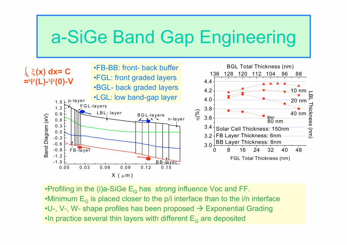
a-SiGe Band Gap Engineering
0 8 16 24 32 40 483.0
3.2
3.4
3.6
3.8
4.0
4.2
4.4
LBL Thickness (nm)
10 nm
FGL Total Thickness (nm)
η(%
)
136 128 120 112 104 96 88
80 nmSolar Cell Thickness: 150nmFB Layer Thickness: 6nmBB Layer Thickness: 8nm
20 nm
40 nm80 nm
BGL Total Thickness (nm)
0 .0 0 0 .0 3 0 .0 6 0 .0 9 0 .1 2 0 .1 5-1 .5-1 .2-0 .9-0 .6-0 .30 .00 .30 .60 .91 .21 .5
L B L - la ye r B G L -la ye rs
F G L -la ye rs
B B -la ye r
F B -la ye r
n - la ye r
p - la ye r
Band
Dia
gram
(eV)
X ( µm )
•Profiling in the (i)a-SiGe EG has strong influence Voc and FF.•Minimum EG is placed closer to the p/i interface than to the i/n interface•U-, V-, W- shape profiles has been proposed Exponential Grading•In practice several thin layers with different EG are deposited
•FB-BB: front- back buffer•FGL: front graded layers•BGL- back graded layers•LGL: low band-gap layer
∫L ξ(x) dx= C=Ψ(L)-Ψ(0)-V

Some conclusions
• Computer modeling allow us to explain the physics behind of somecharacteristic signatures present in the J-V and SR curves of different cell structures.
• The code calibration made by relying in simple cell structures have to be re-adapted to be used in more complex devices.
• More elaborate physical models do not necessarily lead us to a better fitting and interpretation of experimental results.
• Lack of agreement between computer predictions and experiments could teach us what is missing in our modeling.
• Cell structures to be modeled are becoming more complex.• Numerical modeling is a very time consuming task.• Computer modeling can be used as prediction tool.• The most fruitful effort is to reproduce the experimental trends rather
than accurate fittings.
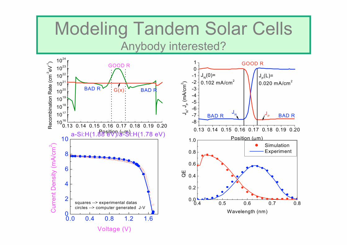
Modeling Tandem Solar CellsAnybody interested?
0.13 0.14 0.15 0.16 0.17 0.18 0.19 0.201016
1017
1018101910201021
10221023
1024
G(x) BAD RBAD R
GOOD R
Rec
ombi
natio
n R
ate
(cm
-3eV
-1)
Position (µm)
0.13 0.14 0.15 0.16 0.17 0.18 0.19 0.20-8-7-6-5-4-3-2-101
JP(L)= 0.020 mA/cm2
JN(0)= 0.102 mA/cm2
BAD RBAD R
GOOD R
JPJNJ N
, JP (m
A/c
m2 )
Position (µm)
0.4 0.5 0.6 0.7 0.80.0
0.2
0.4
0.6
0.8
1.0 Simulation Experiment
QE
Wavelength (nm)
0.0 0.4 0.8 1.2 1.60
2
4
6
8
10
squares --> experimental datascircles --> computer generated J-V
a-Si:H(1.88 eV)/a-Si:H(1.78 eV)
Cur
rent
Den
sity
(mA/
cm2 )
Voltage (V)


![MICROCRYSTALLINE WAX - ::krishna::krishna.nic.in/PDFfiles/MSME/Chemical/MICROCRYSTALLINE WAX[1].pdf · Specification of Microcrystalline wax ... MRF Ltd. 1.000 43372 ... The content](https://static.fdocuments.net/doc/165x107/5aa76b097f8b9ac5648c1342/microcrystalline-wax-krishna-wax1pdfspecification-of-microcrystalline-wax.jpg)


