Computer Architecture 2011 – PC Structure and Peripherals 1 Computer Architecture PC Structure and...
54
Computer Architecture 2011 – PC Structure and Peripherals 1 Computer Architecture PC Structure and Peripherals Dr. Lihu Rappoport
-
Upload
krystal-straker -
Category
Documents
-
view
231 -
download
4
Transcript of Computer Architecture 2011 – PC Structure and Peripherals 1 Computer Architecture PC Structure and...
Computer Architecture 2011 – PC Structure and Peripherals1
Computer Architecture
PC Structure and PeripheralsDr. Lihu Rappoport
Computer Architecture 2011 – PC Structure and Peripherals2
DRAM
Computer Architecture 2011 – PC Structure and Peripherals3
Basic DRAM chip
DRAM access sequence Put Row on addr. bus and assert RAS# (Row Addr. Strobe) to latch
Row Put Column on addr. bus and assert CAS# (Column Addr. Strobe) to
latch Col Get data on address bus
Row Address
Latch
Row Addressdecoder
Column addrdecoder
CAS#
RAS#
Data
MemoryarrayAddr
ColumnAddress
Latch
Computer Architecture 2011 – PC Structure and Peripherals4
DRAM Operation DRAM cell consists of transistor +
capacitor Capacitor keeps the state;
Transistor guards access to the state Reading cell state:
raise access line AL and sense DL• Capacitor charged
current to flow on the data line DL Writing cell state:
set DL and raise AL to charge/drain capacitor
Charging and draining a capacitor is not instantaneous
Leakage current drains capacitor even when transistor is closed
DRAM cell periodically refreshed every 64ms
AL
DLCM

Computer Architecture 2011 – PC Structure and Peripherals5
DRAM Access Sequence Timing
Put row address on address bus and assert RAS# Wait for RAS# to CAS# delay (tRCD) between asserting RAS
and CAS Put column address on address bus and assert CAS# Wait for CAS latency (CL) between time CAS# asserted and
data ready Row precharge time: time to close current row, and open a new
row
tRCD – RAS/CAS delay
tRP – Row Precharge
RAS#
Data
A[0:7]
CAS#
Data n
Row i Col n Row jX
CL – CAS latency
X
Computer Architecture 2011 – PC Structure and Peripherals6
DRAM controller DRAM controller gets address and command
Splits address to Row and Column Generates DRAM control signals at the proper timing
DRAM data must be periodically refreshed DRAM controller performs DRAM refresh, using refresh counter
DRAM
addressdecoder
Timedelaygen.
addressmux
RAS#
CAS#
R/W#
A[20:23]
A[10:19]
A[0:9]
Memory address busD[0:7]
Select
Chipselect
Computer Architecture 2011 – PC Structure and Peripherals7
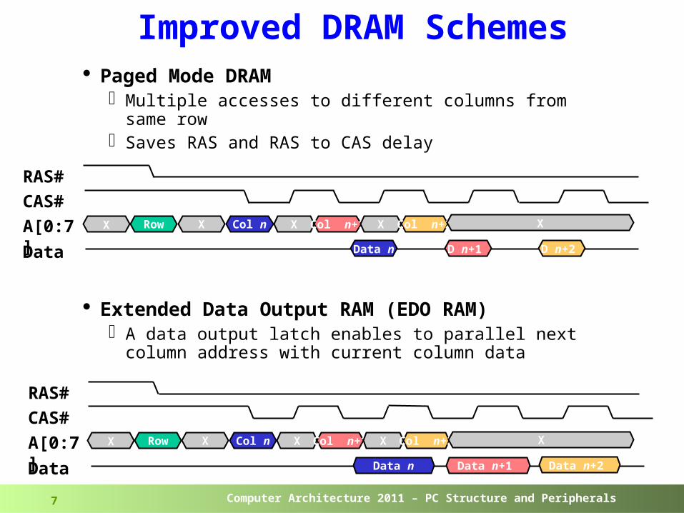
· Paged Mode DRAM– Multiple accesses to different columns from same row– Saves RAS and RAS to CAS delay
· Extended Data Output RAM (EDO RAM)– A data output latch enables to parallel next column address with
current column data
Improved DRAM Schemes
RAS#
Data
A[0:7]
CAS#
Data n D n+1
Row X Col n X Col n+1 X Col n+2 X
D n+2
X
RAS#
Data
A[0:7]
CAS#
Data n Data n+1
Row X Col n X Col n+1 X Col n+2 X
Data n+2
X
Computer Architecture 2011 – PC Structure and Peripherals8
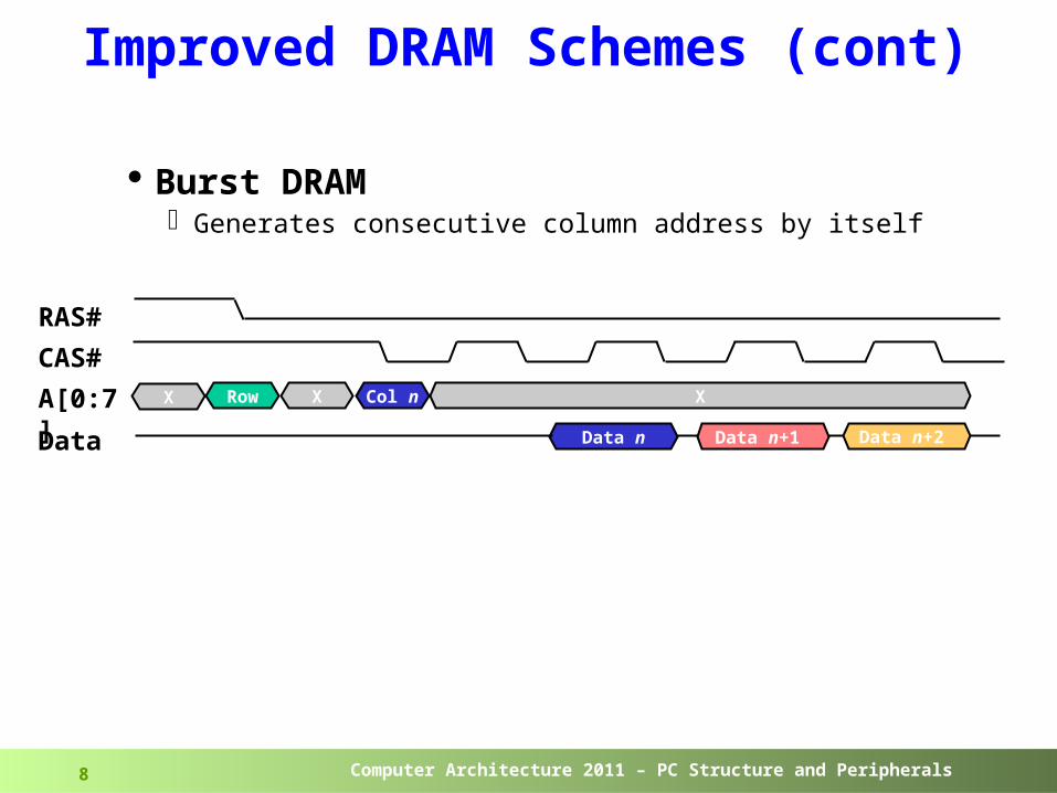
· Burst DRAM– Generates consecutive column address by itself
Improved DRAM Schemes (cont)
RAS#
Data
A[0:7]
CAS#
Data n Data n+1
Row X Col n X
Data n+2
X
Computer Architecture 2011 – PC Structure and Peripherals9
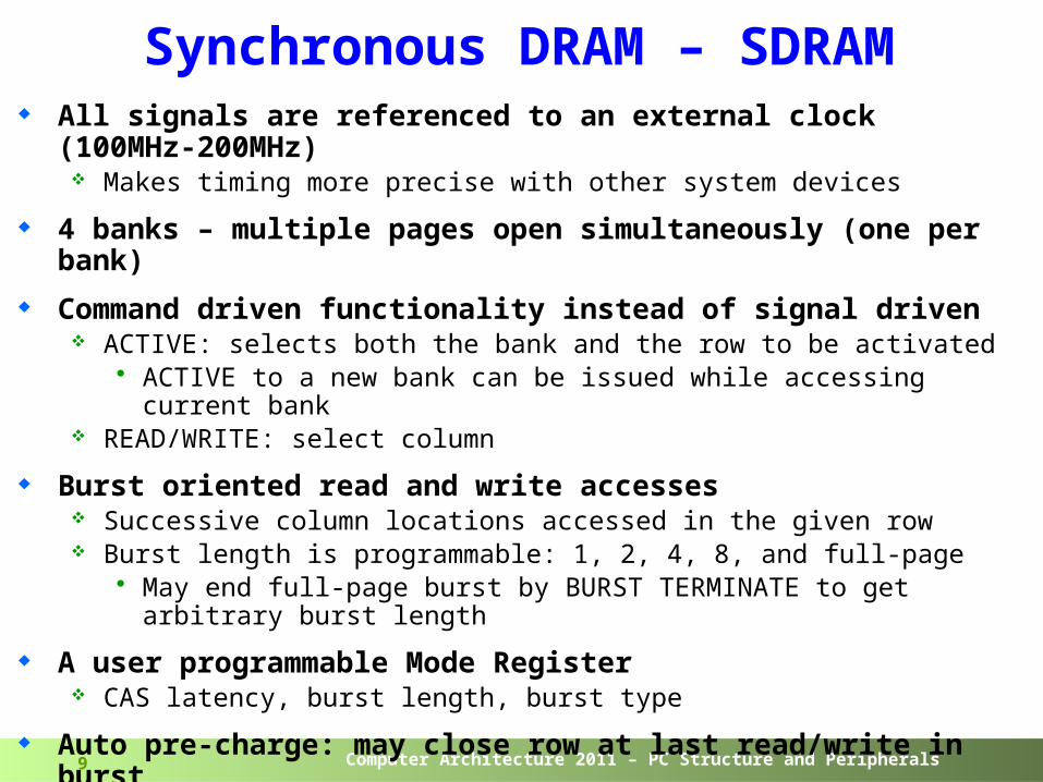
Synchronous DRAM – SDRAM All signals are referenced to an external clock (100MHz-
200MHz) Makes timing more precise with other system devices
4 banks – multiple pages open simultaneously (one per bank)
Command driven functionality instead of signal driven ACTIVE: selects both the bank and the row to be activated
• ACTIVE to a new bank can be issued while accessing current bank READ/WRITE: select column
Burst oriented read and write accesses Successive column locations accessed in the given row Burst length is programmable: 1, 2, 4, 8, and full-page
• May end full-page burst by BURST TERMINATE to get arbitrary burst length
A user programmable Mode Register CAS latency, burst length, burst type
Auto pre-charge: may close row at last read/write in burst
Auto refresh: internal counters generate refresh address
Computer Architecture 2011 – PC Structure and Peripherals10
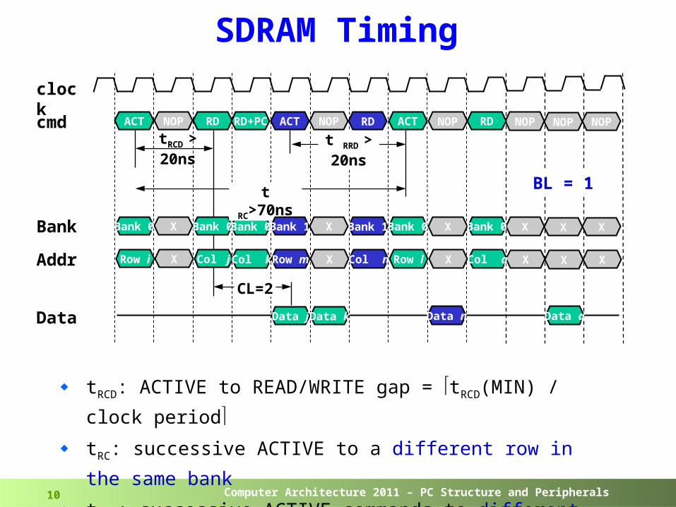
SDRAM Timing
tRCD: ACTIVE to READ/WRITE gap = tRCD(MIN) / clock
period tRC: successive ACTIVE to a different row in the same
bank
tRRD: successive ACTIVE commands to different banks
clock
cmd
Bank
Data
Addr
NOP
X
Data j Data k
ACT
Bank 0
Row i X
RD
Bank 0
Col j
tRCD >20ns
RD+PC
Bank 0
Col k
ACT
Bank 0
Row l
t RC>70ns
ACT
Bank 1
Row m
t RRD >20ns
CL=2
NOP
X
X
NOP
X
X
NOP
X
X
RD
Bank 0
Col q
RD
Bank 1
Col n
NOP
X
X
NOP
X
X
Data n Data q
BL = 1
Computer Architecture 2011 – PC Structure and Peripherals11
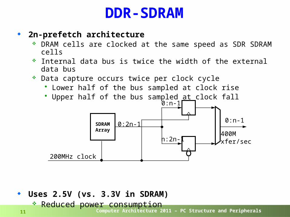
DDR-SDRAM 2n-prefetch architecture
DRAM cells are clocked at the same speed as SDR SDRAM cells Internal data bus is twice the width of the external data bus Data capture occurs twice per clock cycle
• Lower half of the bus sampled at clock rise• Upper half of the bus sampled at clock fall
Uses 2.5V (vs. 3.3V in SDRAM) Reduced power consumption
n:2n-1
0:n-1
0:n-1
200MHz clock
0:2n-1SDRAMArray
400Mxfer/sec
Computer Architecture 2011 – PC Structure and Peripherals12
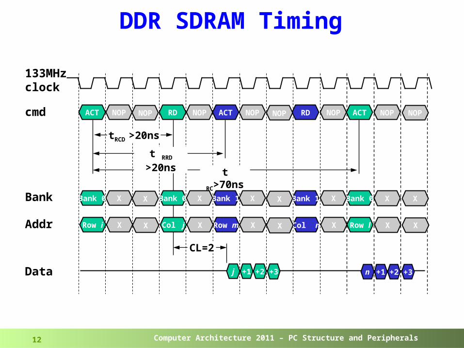
DDR SDRAM Timing
133MHzclock
cmd
Bank
Data
Addr
NOP
X
ACT
Bank 0
Row i X
RD
Bank 0
Col j
tRCD >20ns
ACT
Bank 0
Row l
t RC>70ns
ACT
Bank 1
Row m
t RRD >20ns
CL=2
NOP
X
X
NOP
X
X
NOP
X
X
RD
Bank 1
Col n
NOP
X
X
NOP
X
X
NOP
X
X
NOP
X
X
j +1 +2 +3 n +1 +2 +3
Computer Architecture 2011 – PC Structure and Peripherals13
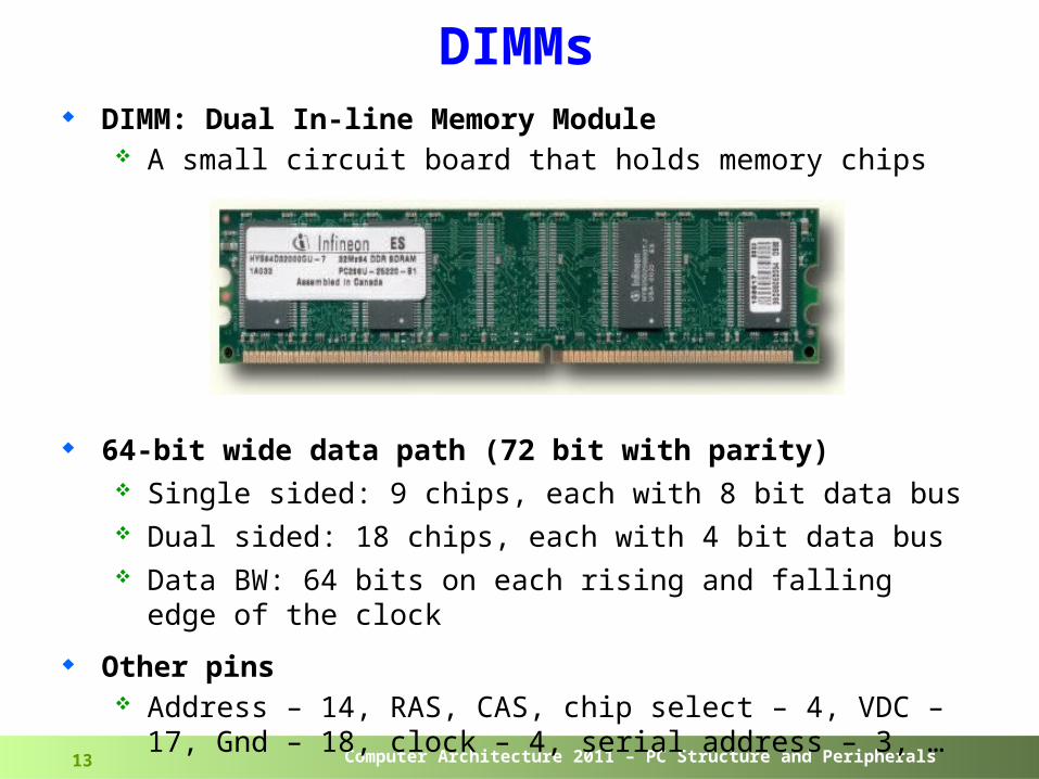
DIMMs DIMM: Dual In-line Memory Module
A small circuit board that holds memory chips
64-bit wide data path (72 bit with parity) Single sided: 9 chips, each with 8 bit data bus Dual sided: 18 chips, each with 4 bit data bus Data BW: 64 bits on each rising and falling edge of the
clock
Other pins Address – 14, RAS, CAS, chip select – 4, VDC – 17, Gnd –
18, clock – 4, serial address – 3, …
Computer Architecture 2011 – PC Structure and Peripherals14
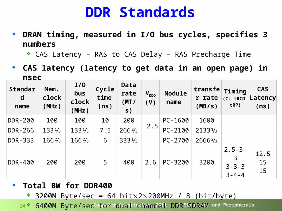
DDR Standards DRAM timing, measured in I/O bus cycles, specifies 3
numbers CAS Latency – RAS to CAS Delay – RAS Precharge Time
CAS latency (latency to get data in an open page) in nsec
CAS Latency × I/O bus cycle time
Total BW for DDR400 3200M Byte/sec = 64 bit2200MHz / 8 (bit/byte) 6400M Byte/sec for dual channel DDR SDRAM
Standard
name
Mem. clock(MHz)
I/O bus clock(MHz)
Cycle time
(ns)
Data rate
(MT/s)
VDDQ
(V)Module name
transfer rate(MB/s)
Timing(CL-tRCD-
tRP)
CAS Latenc
y(ns)
DDR-200 100 100 10 200
2.5
PC-1600 1600
DDR-266 133⅓ 133⅓ 7.5 266⅔ PC-2100 2133⅓
DDR-333 166⅔ 166⅔ 6 333⅓ PC-2700 2666⅔
DDR-400 200 200 5 400 2.6 PC-3200 32002.5-3-33-3-33-4-4
12.51515
Computer Architecture 2011 – PC Structure and Peripherals15
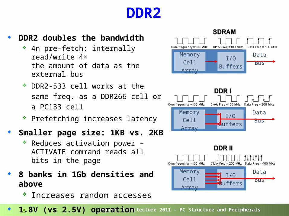
DDR2 DDR2 doubles the bandwidth
4n pre-fetch: internally read/write 4× the amount of data as the external bus
DDR2-533 cell works at the same freq. as a DDR266 cell or a PC133 cell
Prefetching increases latency
Smaller page size: 1KB vs. 2KB Reduces activation power –
ACTIVATE command reads all bits in the page
8 banks in 1Gb densities and above Increases random accesses
1.8V (vs 2.5V) operation voltage
Significantly lower power
Memory
Cell Array
I/O
BuffersData Bus
Memory
Cell Array
I/O
BuffersData Bus
Memory
Cell Array
I/O
BuffersData Bus
Computer Architecture 2011 – PC Structure and Peripherals16
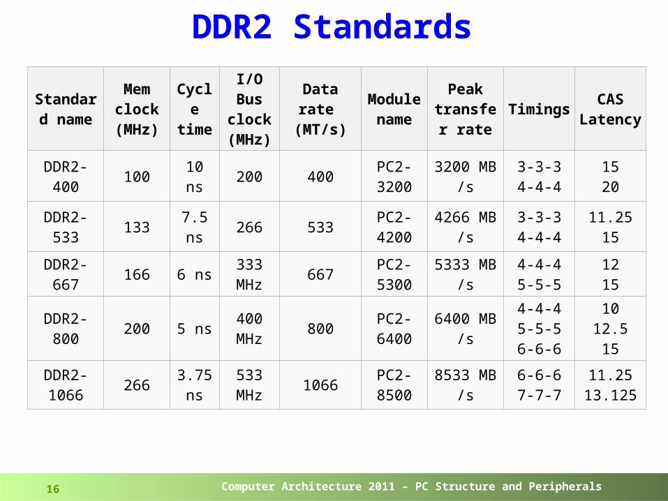
DDR2 Standards
Standard name
Mem clock(MHz)
Cycle
time
I/O Bus
clock(MHz)
Data rate
(MT/s)
Module
name
Peak transfer
rate
Timings
CASLatenc
y
DDR2-400 100 10 ns 200 400 PC2-
32003200 MB
/s3-3-34-4-4
1520
DDR2-533 133 7.5
ns 266 533 PC2-4200
4266 MB/s
3-3-34-4-4
11.2515
DDR2-667 166 6 ns 333
MHz 667 PC2-5300
5333 MB/s
4-4-45-5-5
1215
DDR2-800 200 5 ns 400
MHz 800 PC2-6400
6400 MB/s
4-4-45-5-56-6-6
1012.515
DDR2-1066 266 3.75
ns533 MHz 1066 PC2-
85008533 MB
/s6-6-67-7-7
11.2513.125
Computer Architecture 2011 – PC Structure and Peripherals17
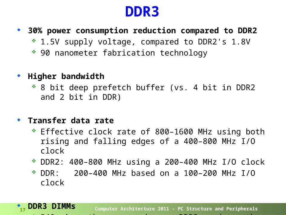
DDR3 30% power consumption reduction compared to
DDR2 1.5V supply voltage, compared to DDR2's 1.8V 90 nanometer fabrication technology
Higher bandwidth 8 bit deep prefetch buffer (vs. 4 bit in DDR2 and 2 bit in
DDR)
Transfer data rate Effective clock rate of 800–1600 MHz using both rising
and falling edges of a 400–800 MHz I/O clock DDR2: 400–800 MHz using a 200–400 MHz I/O clock DDR: 200–400 MHz based on a 100–200 MHz I/O clock
DDR3 DIMMs 240 pins, the same number as DDR2, and are the same
size Electrically incompatible, and have a different key notch
location
Computer Architecture 2011 – PC Structure and Peripherals18
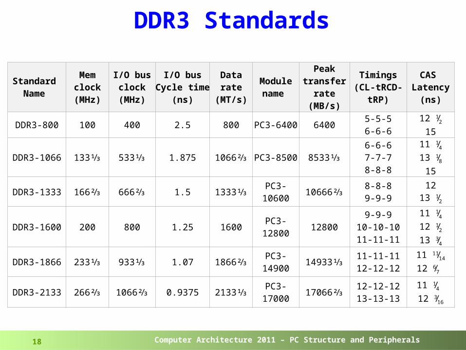
DDR3 Standards
Standard Name
Mem clock(MHz)
I/O bus clock(MHz)
I/O busCycle time
(ns)
Data rate
(MT/s)
Module name
Peak transfer
rate(MB/s)
Timings(CL-tRCD-
tRP)
CAS Latency
(ns)
DDR3-800 100 400 2.5 800 PC3-6400 64005-5-56-6-6
12 1⁄215
DDR3-1066 133⅓ 533⅓ 1.875 1066⅔ PC3-8500 8533⅓6-6-67-7-78-8-8
11 1⁄413 1⁄815
DDR3-1333 166⅔ 666⅔ 1.5 1333⅓PC3-
1060010666⅔
8-8-89-9-9
1213 1⁄2
DDR3-1600 200 800 1.25 1600PC3-
1280012800
9-9-910-10-1011-11-11
11 1⁄412 1⁄213 3⁄4
DDR3-1866 233⅓ 933⅓ 1.07 1866⅔PC3-
1490014933⅓
11-11-1112-12-12
11 11⁄14
12 6⁄7
DDR3-2133 266⅔ 1066⅔ 0.9375 2133⅓PC3-
1700017066⅔
12-12-1213-13-13
11 1⁄4 12 3⁄16
Computer Architecture 2011 – PC Structure and Peripherals19
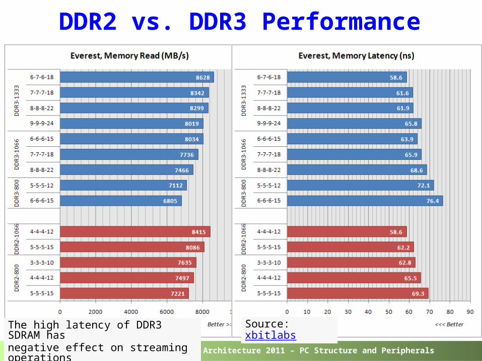
DDR2 vs. DDR3 Performance
The high latency of DDR3 SDRAM has negative effect on streaming operations
Source: xbitlabs
Computer Architecture 2011 – PC Structure and Peripherals20
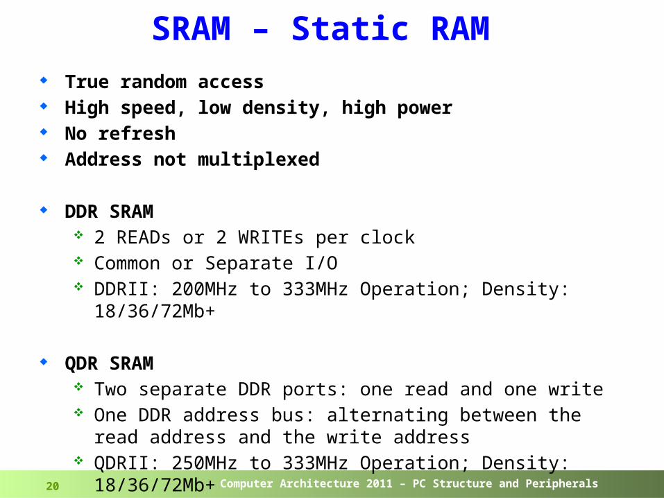
SRAM – Static RAM True random access High speed, low density, high power No refresh Address not multiplexed
DDR SRAM 2 READs or 2 WRITEs per clock Common or Separate I/O DDRII: 200MHz to 333MHz Operation; Density:
18/36/72Mb+
QDR SRAM Two separate DDR ports: one read and one write One DDR address bus: alternating between the read
address and the write address QDRII: 250MHz to 333MHz Operation; Density:
18/36/72Mb+
Computer Architecture 2011 – PC Structure and Peripherals21
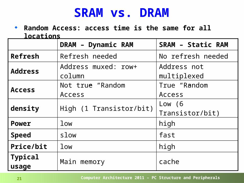
SRAM vs. DRAM Random Access: access time is the same for all
locationsDRAM – Dynamic RAM SRAM – Static RAM
Refresh Refresh needed No refresh needed
Address Address muxed: row+ column
Address not multiplexed
Access Not true “Random Access” True “Random Access”
density High (1 Transistor/bit) Low (6 Transistor/bit)
Power low high
Speed slow fast
Price/bit low high
Typical usage Main memory cache
Computer Architecture 2011 – PC Structure and Peripherals22
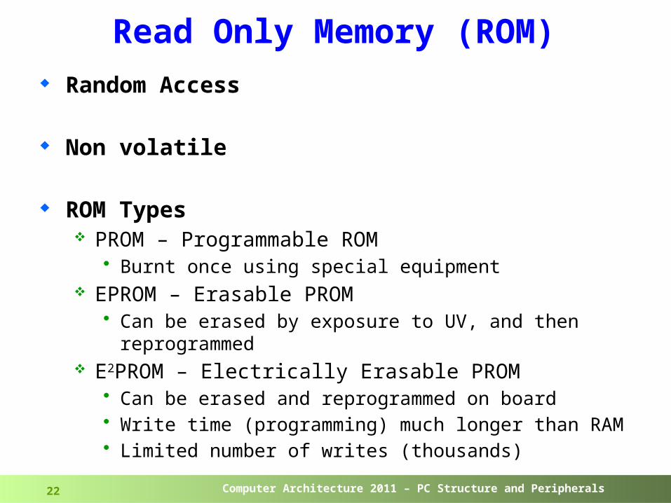
Read Only Memory (ROM) Random Access
Non volatile
ROM Types PROM – Programmable ROM
• Burnt once using special equipment EPROM – Erasable PROM
• Can be erased by exposure to UV, and then reprogrammed
E2PROM – Electrically Erasable PROM• Can be erased and reprogrammed on board• Write time (programming) much longer than RAM• Limited number of writes (thousands)
Computer Architecture 2011 – PC Structure and Peripherals23
Hard Disks
Computer Architecture 2011 – PC Structure and Peripherals24
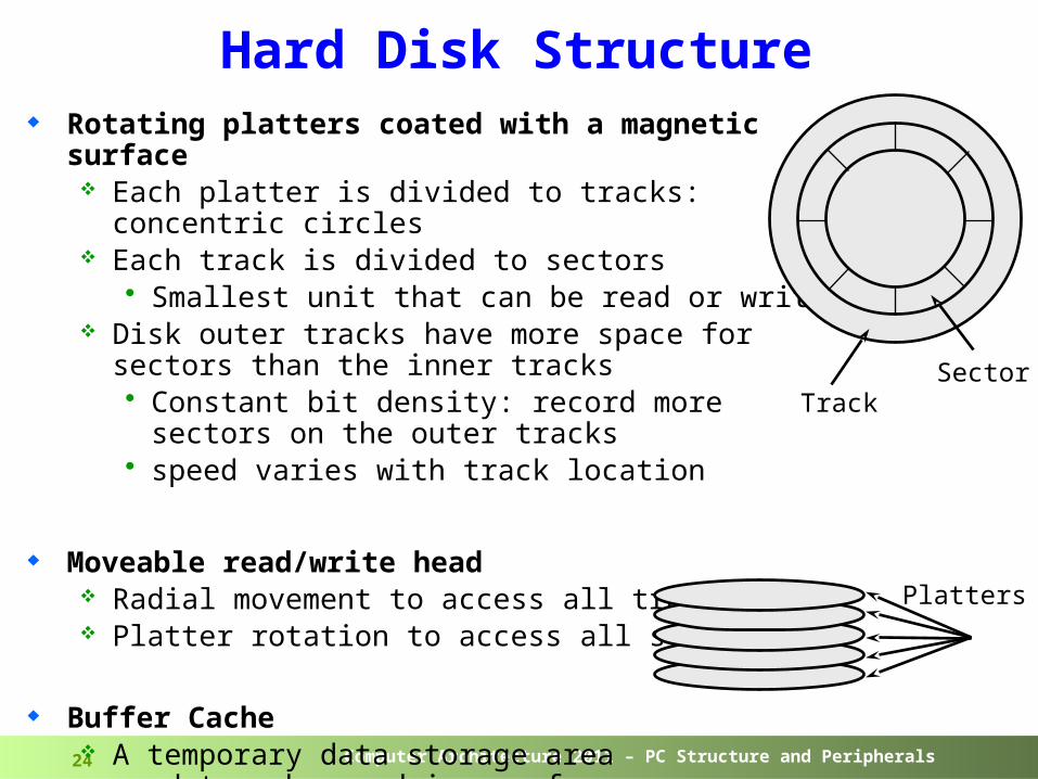
Hard Disk Structure Rotating platters coated with a magnetic surface
Each platter is divided to tracks: concentric circles Each track is divided to sectors
• Smallest unit that can be read or written Disk outer tracks have more space for
sectors than the inner tracks• Constant bit density: record more
sectors on the outer tracks• speed varies with track location
Moveable read/write head Radial movement to access all tracks Platter rotation to access all sectors
Buffer Cache A temporary data storage area
used to enhance drive performance
Platters
TrackSector
Computer Architecture 2011 – PC Structure and Peripherals25
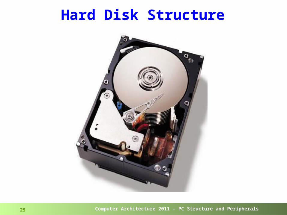
Hard Disk Structure
Computer Architecture 2011 – PC Structure and Peripherals26
Disk Access Seek: position the head over the proper track
Average: Sum of the time for all possible seek / total # of possible seeks
Due to locality of disk reference, actual average seek is shorter: 4 to 12 ms
Rotational latency: wait for desired sector to rotate under head The faster the drives spins, the shorter the rotational latency time Most disks rotate at 5,400 to 15,000 RPM
• At 7200 RPM: 8 ms per revolution An average latency to the desired information is halfway around the
disk• At 7200 RPM: 4 ms
Transfer block: read/write the data Transfer time is a function of: sector size, rotation speed,
and recording density: bits per inch on a track Typical values: 100 MB / sec
Disk Access Time = Seek time + Rotational Latency + Transfer time + Controller Time + Queuing Delay
Computer Architecture 2011 – PC Structure and Peripherals27
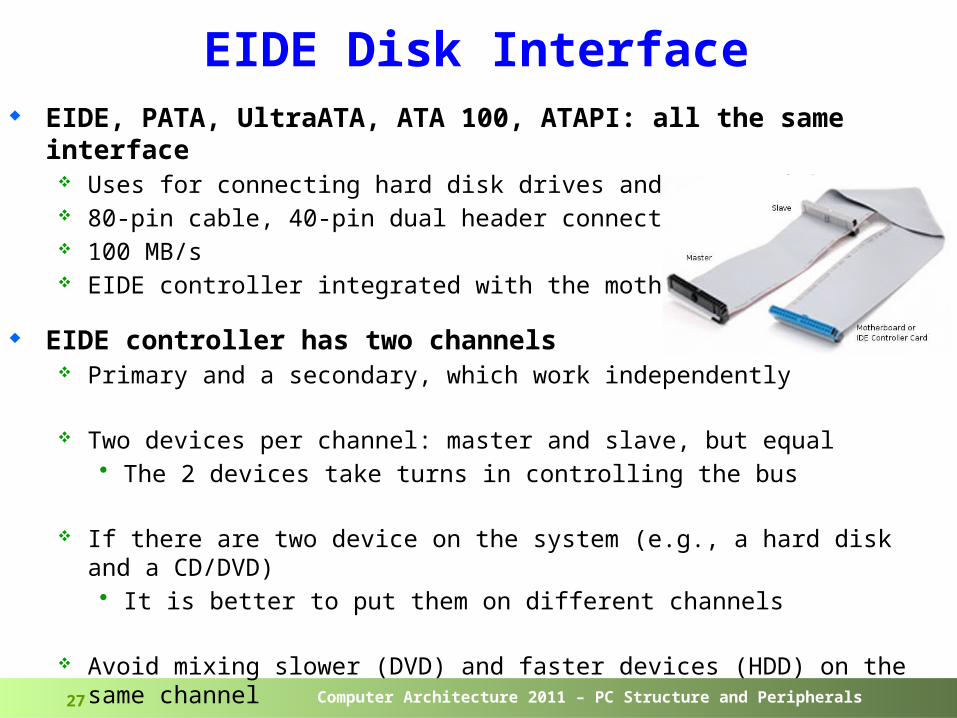
EIDE Disk Interface EIDE, PATA, UltraATA, ATA 100, ATAPI: all the same
interface Uses for connecting hard disk drives and CD/DVD drives 80-pin cable, 40-pin dual header connector 100 MB/s EIDE controller integrated with the motherboard
EIDE controller has two channels Primary and a secondary, which work independently
Two devices per channel: master and slave, but equal• The 2 devices take turns in controlling the bus
If there are two device on the system (e.g., a hard disk and a CD/DVD)• It is better to put them on different channels
Avoid mixing slower (DVD) and faster devices (HDD) on the same channel
If doing a lot of copying from drive to drive• Better performance by separating devices to separate channels
Computer Architecture 2011 – PC Structure and Peripherals28
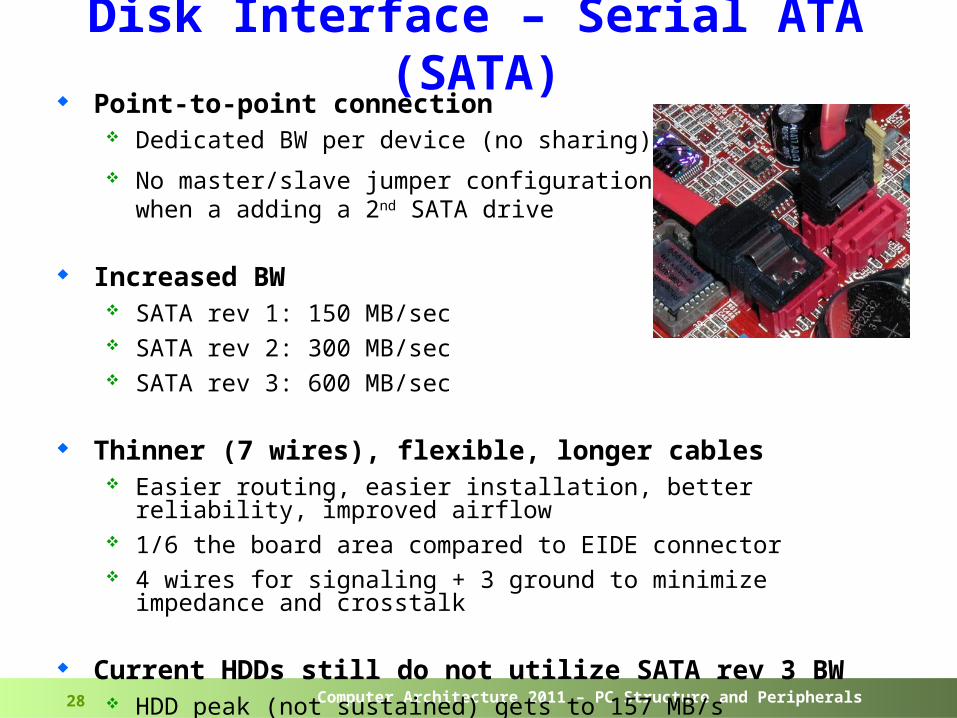
Disk Interface – Serial ATA (SATA) Point-to-point connection
Dedicated BW per device (no sharing) No master/slave jumper configuration needed
when a adding a 2nd SATA drive
Increased BW SATA rev 1: 150 MB/sec SATA rev 2: 300 MB/sec SATA rev 3: 600 MB/sec
Thinner (7 wires), flexible, longer cables Easier routing, easier installation, better reliability, improved
airflow 1/6 the board area compared to EIDE connector 4 wires for signaling + 3 ground to minimize impedance and
crosstalk
Current HDDs still do not utilize SATA rev 3 BW HDD peak (not sustained) gets to 157 MB/s SSD gets to 250 MB/sec
Computer Architecture 2011 – PC Structure and Peripherals29
Flash Memory Flash is a non-volatile, rewritable memory
NOR Flash Supports per-byte data read and write (random access)
• Erasing (setting all the bits) done only at block granularity (64-128KB)
• Writing (clearing a bit) can be done at byte granularity Suitable for storing code (e.g. BIOS, cell phone firmware)
NAND Flash Supports page-mode read and write (0.5KB – 4KB per page)
• Erasing (setting all the bits) done only at block granularity (64-128KB)
Suitable for storing large data (e.g. pictures, songs)• Similar to other secondary data storage devices
Reduced erase and write times Greater storage density and lower cost per bit
Computer Architecture 2011 – PC Structure and Peripherals30
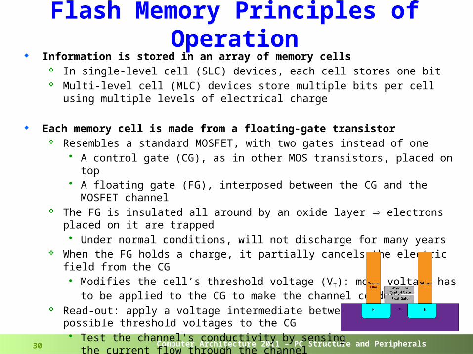
Flash Memory Principles of Operation
Information is stored in an array of memory cells In single-level cell (SLC) devices, each cell stores one bit Multi-level cell (MLC) devices store multiple bits per cell using multiple
levels of electrical charge
Each memory cell is made from a floating-gate transistor Resembles a standard MOSFET, with two gates instead of one
• A control gate (CG), as in other MOS transistors, placed on top• A floating gate (FG), interposed between the CG and the MOSFET
channel The FG is insulated all around by an oxide layer electrons placed on it
are trapped • Under normal conditions, will not discharge for many years
When the FG holds a charge, it partially cancels the electric field from the CG• Modifies the cell’s threshold voltage (VT): more voltage has to be
applied to the CG to make the channel conduct Read-out: apply a voltage intermediate between the
possible threshold voltages to the CG• Test the channel's conductivity by sensing
the current flow through the channel• In a MLC device, sense the amount of current flow
Computer Architecture 2011 – PC Structure and Peripherals31
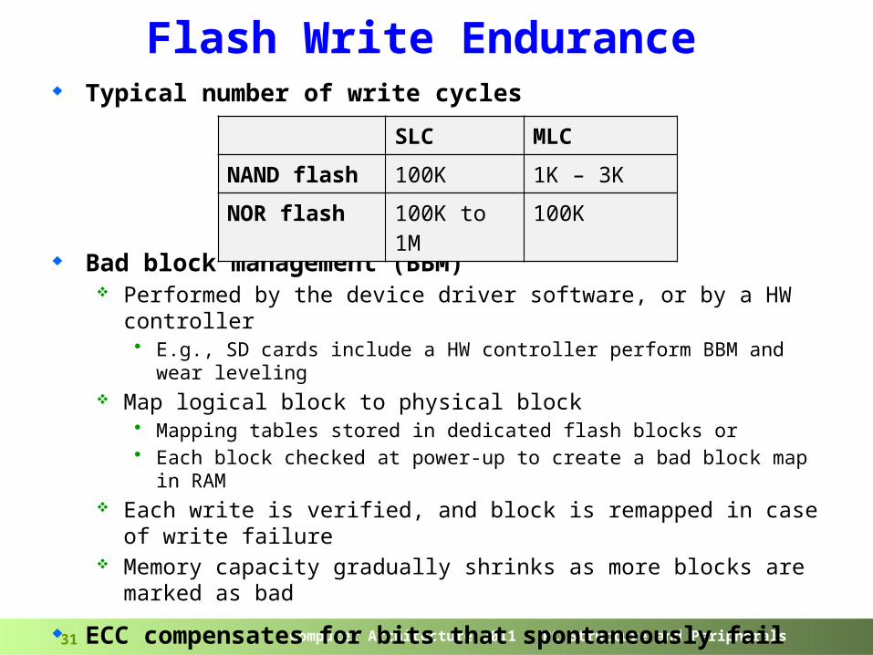
Flash Write Endurance Typical number of write cycles
Bad block management (BBM) Performed by the device driver software, or by a HW controller
• E.g., SD cards include a HW controller perform BBM and wear leveling
Map logical block to physical block • Mapping tables stored in dedicated flash blocks or • Each block checked at power-up to create a bad block map in RAM
Each write is verified, and block is remapped in case of write failure
Memory capacity gradually shrinks as more blocks are marked as bad
ECC compensates for bits that spontaneously fail 22 (24) bits of ECC code correct a one bit error in 2048 (4096)
data bits If ECC cannot correct the error during read, it may still detect
the error
SLC MLC
NAND flash 100K 1K – 3K
NOR flash 100K to 1M
100K
Computer Architecture 2011 – PC Structure and Peripherals32
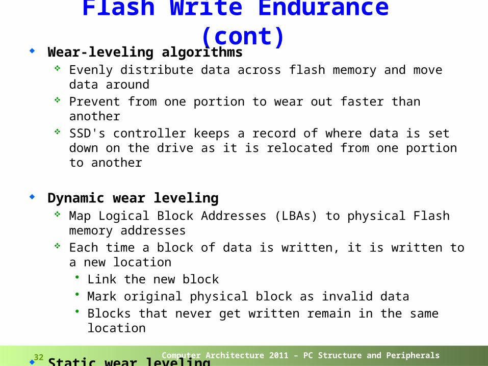
Flash Write Endurance (cont) Wear-leveling algorithms
Evenly distribute data across flash memory and move data around
Prevent from one portion to wear out faster than another SSD's controller keeps a record of where data is set down on the
drive as it is relocated from one portion to another
Dynamic wear leveling Map Logical Block Addresses (LBAs) to physical Flash memory
addresses Each time a block of data is written, it is written to a new
location• Link the new block • Mark original physical block as invalid data• Blocks that never get written remain in the same location
Static wear leveling Periodically move blocks which are not written Allow these low usage cells be used by other data
Computer Architecture 2011 – PC Structure and Peripherals33
Solid State Drive – SSD Most manufacturers use "burst rate" for Performance
numbers Not its steady state or average read rate
Any write operation requires an erase followed by the write When SSD is new, NAND flash memory is pre-erased
Consumer-grade multi-level cell (MLC) Allows ≥2 bit per flash memory cell Sustains 2,000 to 10,000 write cycles Notably less expensive than SLC drives
Enterprise-class single-level cell (SLC) Allows 1 bit per flash memory cell Lasts 10× write cycles of an MLC
The more write/erase cycle the shorter the drive's lifespan Use wear-leveling algorithms to evenly distribute writes DRAM cache to buffer data writes to reduce number of
write/erase cycles Extra memory cells to be used when blocks of flash memory
wear out
Computer Architecture 2011 – PC Structure and Peripherals34
SSD (cont.) Data in NAND flash memory organized in fixed size in
blocks When any portion of the data on the drive is changed
• Mark block for deletion in preparation for the new data• Read current data on the block• Redistribute the old data• Lay down the new data in the old block
Old data is rewritten back Typical write amplification is 15 to 20
• For every 1MB of data written to the drive, 15MB to 20MBs of space is actually needed
• Using write combining reduces write amplification to ~10%
Flash drives compared to HD drives: Smaller size, faster, lighter, noiseless, lower power Withstanding shocks up to 2000 Gs (like 10 foot drop onto
concrete) More expensive (cost/byte): ~2$/1GB vs ~0.1$/1GB in HDD
Computer Architecture 2011 – PC Structure and Peripherals35
The Motherboard
Computer Architecture 2011 – PC Structure and Peripherals36
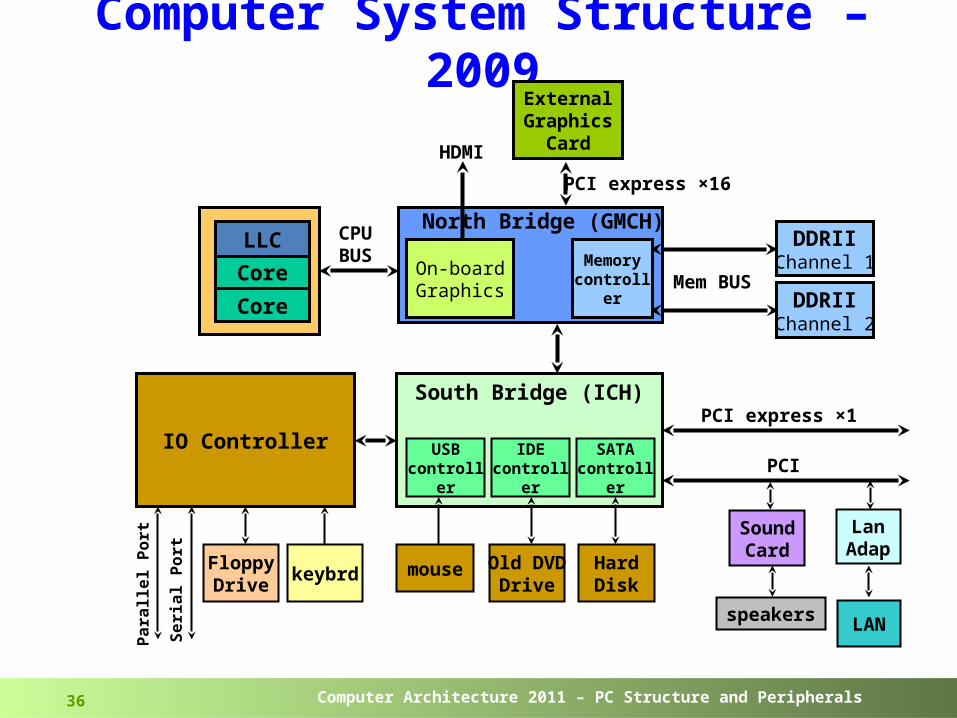
Computer System Structure – 2009
Core
PCI
North Bridge (GMCH)DDRII
Channel 1
mouse
LAN
LanAdap
External Graphics
Card
Mem BUS
LLC
SoundCard
speakers
South Bridge (ICH)
PCI express ×16
IDEcontroller
IO Controller
Old DVDDrive
HardDisk
Pa
rall
el
Po
rt
Se
ria
l P
ort Floppy
Drivekeybrd
DDRIIChannel 2
USBcontroller
SATAcontroller
PCI express ×1
Memory controller
On-board Graphics
CPU BUS
Core
HDMI
Computer Architecture 2011 – PC Structure and Peripherals37
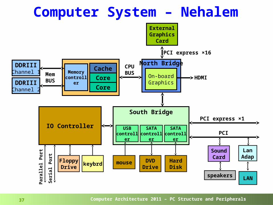
Computer System – Nehalem
PCI
North Bridge
mouse
LAN
LanAdap
External Graphics
Card
CPU BUS
SoundCard
speakers
South Bridge
PCI express ×16
SATAcontroller
IO Controller
DVDDrive
HardDisk
Pa
rall
el
Po
rt
Se
ria
l P
ort Floppy
Drivekeybrd
USBcontroller
SATAcontroller
PCI express ×1
On-board Graphics
CacheDDRIII
Channel 1 Mem BUSDDRIII
Channel 2
Memory controller Core
Core
HDMI
Computer Architecture 2011 – PC Structure and Peripherals38
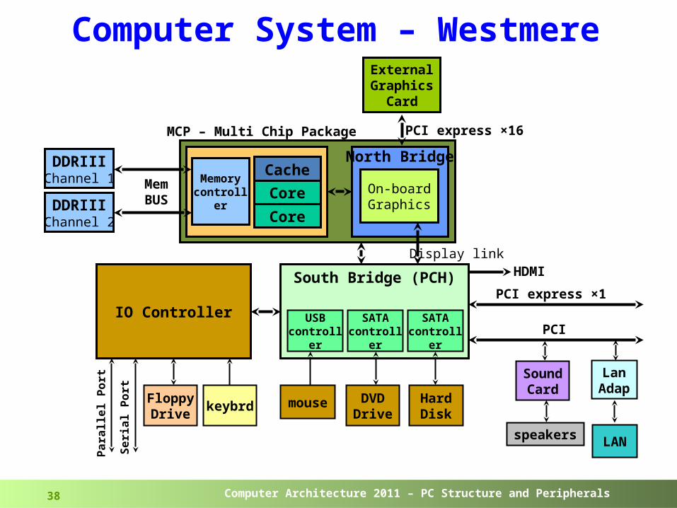
Computer System – Westmere
PCI
North Bridge
mouse
LAN
LanAdap
External Graphics
Card
SoundCard
speakers
South Bridge (PCH)
PCI express ×16
SATAcontroller
IO Controller
DVDDrive
HardDisk
Pa
rall
el
Po
rt
Se
ria
l P
ort Floppy
Drivekeybrd
USBcontroller
SATAcontroller
PCI express ×1
On-board Graphics
CacheDDRIII
Channel 1 Mem BUSDDRIII
Channel 2
Memory controller Core
Core
HDMI
MCP – Multi Chip Package
Display link

Computer Architecture 2011 – PC Structure and Peripherals39
Computer System – Sandy Bridge
mouseLAN
LanAdap
South Bridge (PCH)Audio Codec
DVDDrive
HardDiskP
ara
lle
l P
ort
Se
ria
l P
ort
FloppyDrive
PS/2keybrd/mouse
CacheDDRIII
Channel 1 Mem BUSDDRIII
Channel 2
Memory controller Core
Core
D-sub, HDMI, DVI, Display port
External Graphics
Card
PCI express ×16
GFX
Display link
2133-1066 MHz
Line inLine out
S/PDIF inS/PDIF out
Super I/OLPC
USB SATA SATA
BIOS PCI express ×1
expslots
System Agent
4×DMI
Computer Architecture 2011 – PC Structure and Peripherals40
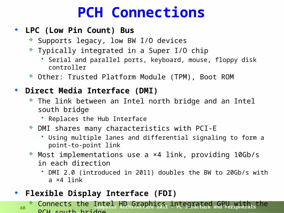
PCH Connections LPC (Low Pin Count) Bus
Supports legacy, low BW I/O devices Typically integrated in a Super I/O chip
• Serial and parallel ports, keyboard, mouse, floppy disk controller Other: Trusted Platform Module (TPM), Boot ROM
Direct Media Interface (DMI) The link between an Intel north bridge and an Intel south bridge
• Replaces the Hub Interface DMI shares many characteristics with PCI-E
• Using multiple lanes and differential signaling to form a point-to-point link
Most implementations use a ×4 link, providing 10Gb/s in each direction • DMI 2.0 (introduced in 2011) doubles the BW to 20Gb/s with a ×4 link
Flexible Display Interface (FDI) Connects the Intel HD Graphics integrated GPU with the PCH
south bridge• where display connectors are attached
Supports 2 independent 4-bit fixed frequency links/channels/pipes at 2.7GT/s data rate
Computer Architecture 2011 – PC Structure and Peripherals41
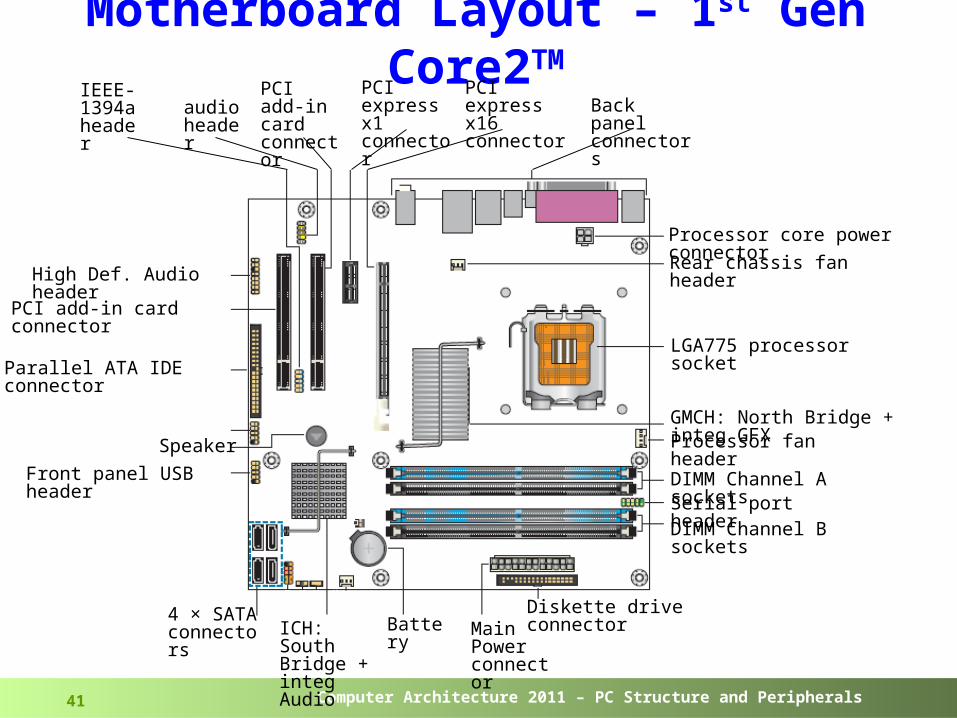
Motherboard Layout – 1st Gen Core2TM
IEEE-1394a header
audio header
PCI add-in card connector
PCI express x1 connector
PCI express x16 connector
Back panel connectors
Processor core power connector
Rear chassis fan header
LGA775 processor socket
GMCH: North Bridge + integ GFXProcessor fan header
DIMM Channel A socketsSerial port headerDIMM Channel B sockets
Diskette drive connectorMain Power connector
BatteryICH: South Bridge + integ Audio
4 × SATA connectors
Front panel USB header
Speaker
Parallel ATA IDE connector
High Def. Audio header
PCI add-in card connector
Computer Architecture 2011 – PC Structure and Peripherals42
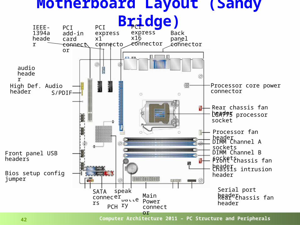
Motherboard Layout (Sandy Bridge)IEEE-
1394a header
audio header
PCI add-in card connector
PCI express x1 connector
PCI express x16 connector
Back panel connectors
Processor core power connector
Rear chassis fan header
LGA775 processor socket
Processor fan header
DIMM Channel A sockets
Serial port header
DIMM Channel B sockets
Main Power connector
BatteryPCH
SATA connectors
Front panel USB headers
Bios setup config jumper
High Def. Audio headerS/PDIF
speaker
Front chassis fan header
Chassis intrusion header
Rear chassis fan header

Computer Architecture 2011 – PC Structure and Peripherals43
ASUS Sabertooth P67 B3 Sandy Bridge Motherboard
Computer Architecture 2011 – PC Structure and Peripherals44
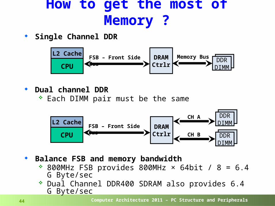
How to get the most of Memory ?
Single Channel DDR
Dual channel DDR Each DIMM pair must be the same
Balance FSB and memory bandwidth 800MHz FSB provides 800MHz × 64bit / 8 = 6.4 G
Byte/sec Dual Channel DDR400 SDRAM also provides 6.4 G
Byte/sec
CH A DDRDIMM
DDRDIMM
CH B
L2 Cache
CPUFSB – Front Side Bus DRAM
Ctrlr
L2 Cache
CPUFSB – Front Side Bus Memory BusDRAM
CtrlrDDRDIMM
Computer Architecture 2011 – PC Structure and Peripherals45
How to get the most of Memory ?
Each DIMM supports 4 open pages simultaneously The more open pages, the more random access It is better to have more DIMMs
• n DIMMs: 4n open pages
DIMMs can be single sided or dual sided Dual sided DIMMs may have separate CS of each side
• In this case the number of open pages is doubled (goes up to 8)
• This is not a must – dual sided DIMMs may also have a common CS for both sides, in which case, there are only 4 open pages, as with single side
Computer Architecture 2011 – PC Structure and Peripherals46
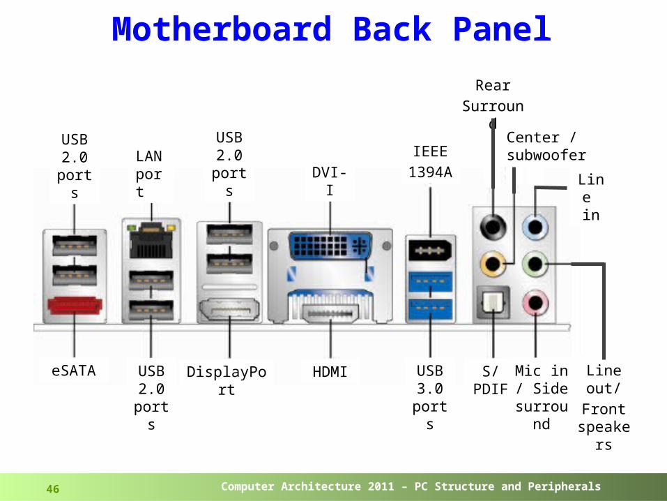
Motherboard Back Panel
USB 2.0 port
s
LANport
USB 2.0 port
s
USB 3.0 port
s
eSATA USB 2.0 port
s
DisplayPort
HDMI
DVI-IIEEE1394
A
RearSurroun
d
Line in
Line out/Front
speakers
S/PDIF
Center /subwoofer
Mic in/ Side
surround
Computer Architecture 2011 – PC Structure and Peripherals47
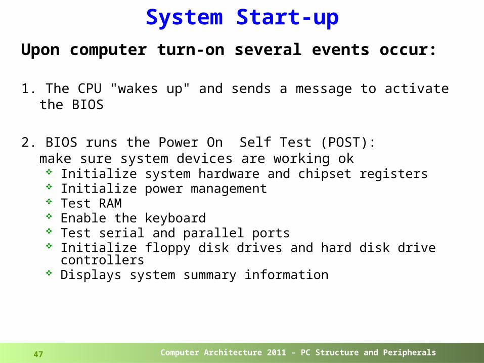
System Start-upUpon computer turn-on several events occur:
1. The CPU "wakes up" and sends a message to activate the BIOS
2. BIOS runs the Power On Self Test (POST): make sure system devices are working ok Initialize system hardware and chipset registers Initialize power management Test RAM Enable the keyboard Test serial and parallel ports Initialize floppy disk drives and hard disk drive controllers Displays system summary information
Computer Architecture 2011 – PC Structure and Peripherals48
System Start-up (cont.)3. During POST, the BIOS compares the system configuration
data obtained from POST with the system information stored on a memory chip located on the MB A CMOS chip, which is updated whenever new system
components are added Contains the latest information about system components
4. After the POST tasks are completed the BIOS looks for the boot program responsible for loading
the operating system Usually, the BIOS looks on the floppy disk drive A: followed
by drive C:
5. After boot program is loaded into memory It loads the system configuration information contained in
the registry in a Windows® environment, and device drivers
6. Finally, the operating system is loaded
Computer Architecture 2011 – PC Structure and Peripherals49
Backup
Computer Architecture 2011 – PC Structure and Peripherals50
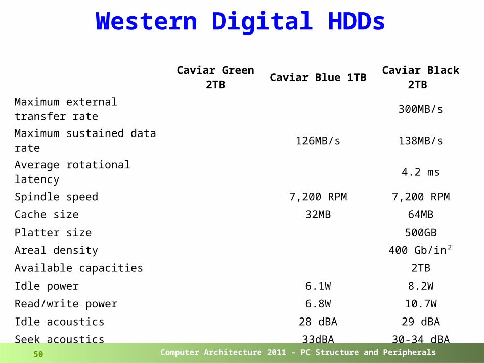
Western Digital HDDs
Caviar Green 2TB Caviar Blue 1TB Caviar Black
2TB
Maximum external transfer rate 300MB/s
Maximum sustained data rate 126MB/s 138MB/s
Average rotational latency 4.2 ms
Spindle speed 7,200 RPM 7,200 RPM
Cache size 32MB 64MB
Platter size 500GB
Areal density 400 Gb/in²
Available capacities 2TB
Idle power 6.1W 8.2W
Read/write power 6.8W 10.7W
Idle acoustics 28 dBA 29 dBA
Seek acoustics 33dBA 30-34 dBA
Computer Architecture 2011 – PC Structure and Peripherals51
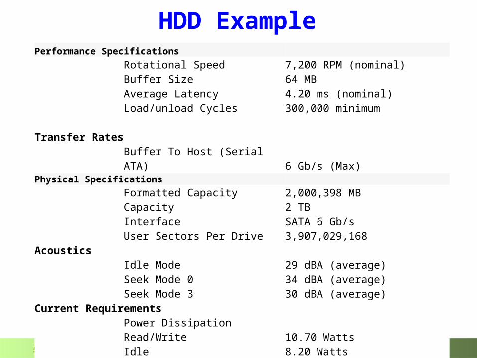
HDD ExamplePerformance Specifications Rotational Speed 7,200 RPM (nominal) Buffer Size 64 MB Average Latency 4.20 ms (nominal) Load/unload Cycles 300,000 minimum Transfer Rates Buffer To Host (Serial ATA) 6 Gb/s (Max)Physical Specifications Formatted Capacity 2,000,398 MB Capacity 2 TB Interface SATA 6 Gb/s User Sectors Per Drive 3,907,029,168Acoustics Idle Mode 29 dBA (average) Seek Mode 0 34 dBA (average) Seek Mode 3 30 dBA (average)Current Requirements Power Dissipation Read/Write 10.70 Watts Idle 8.20 Watts Standby 1.30 Watts Sleep 1.30 Watts
Computer Architecture 2011 – PC Structure and Peripherals52
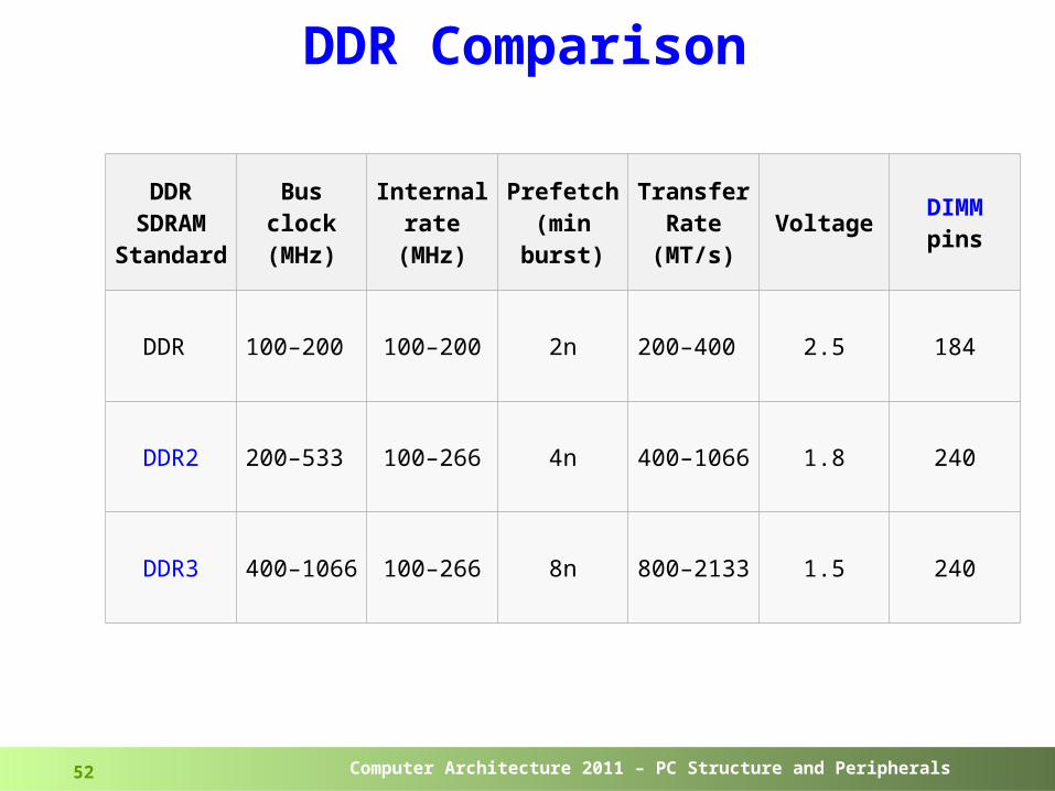
DDR Comparison
DDR SDRAMStandar
d
Bus clock(MHz)
Internal rate
(MHz)
Prefetch(min
burst)
Transfer Rate
(MT/s)Voltage DIMM
pins
DDR 100–200 100–200 2n 200–
400 2.5 184
DDR2 200–533 100–266 4n 400–
1066 1.8 240
DDR3 400–1066 100–266 8n 800–
2133 1.5 240
Computer Architecture 2011 – PC Structure and Peripherals53
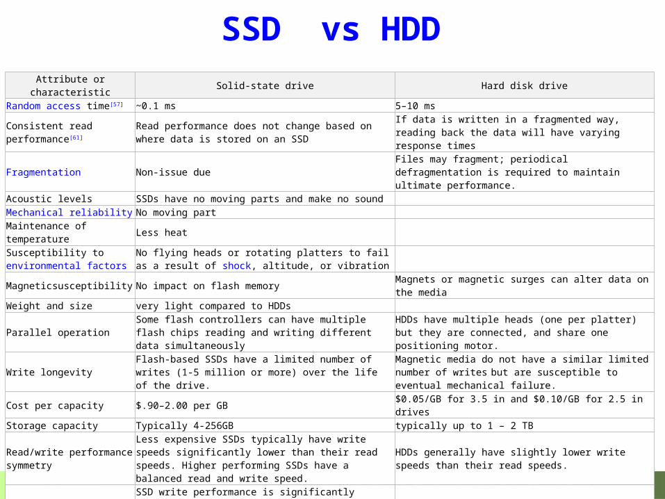
SSD vs HDDAttribute or characteristic Solid-state drive Hard disk driveRandom access time[57] ~0.1 ms 5–10 msConsistent read performance[61]
Read performance does not change based on where data is stored on an SSD
If data is written in a fragmented way, reading back the data will have varying response times
Fragmentation Non-issue dueFiles may fragment; periodical defragmentation is required to maintain ultimate performance.
Acoustic levels SSDs have no moving parts and make no soundMechanical reliability No moving partMaintenance of temperature
Less heat
Susceptibility to environmental factors
No flying heads or rotating platters to fail as a result of shock, altitude, or vibration
Magneticsusceptibility No impact on flash memoryMagnets or magnetic surges can alter data on the media
Weight and size very light compared to HDDs
Parallel operationSome flash controllers can have multiple flash chips reading and writing different data simultaneously
HDDs have multiple heads (one per platter) but they are connected, and share one positioning motor.
Write longevityFlash-based SSDs have a limited number of writes (1-5 million or more) over the life of the drive.
Magnetic media do not have a similar limited number of writes but are susceptible to eventual mechanical failure.
Cost per capacity $.90–2.00 per GB $0.05/GB for 3.5 in and $0.10/GB for 2.5 in drivesStorage capacity Typically 4-256GB typically up to 1 – 2 TB
Read/write performance symmetry
Less expensive SSDs typically have write speeds significantly lower than their read speeds. Higher performing SSDs have a balanced read and write speed.
HDDs generally have slightly lower write speeds than their read speeds.
Free block availability and TRIM
SSD write performance is significantly impacted by the availability of free, programmable blocks. Previously written data blocks that are no longer in use can be reclaimed by TRIM; however, even with TRIM, fewer free, programmable blocks translates into reduced performance.[29][75][76]
HDDs are not affected by free blocks or the operation (or lack) of the TRIM command
Power consumptionHigh performance flash-based SSDs generally require 1/2 to 1/3 the power of HDDs
High performance HDDs require 12-18 watts; drives designed for notebook computers are typically 2 watts.
Computer Architecture 2011 – PC Structure and Peripherals54
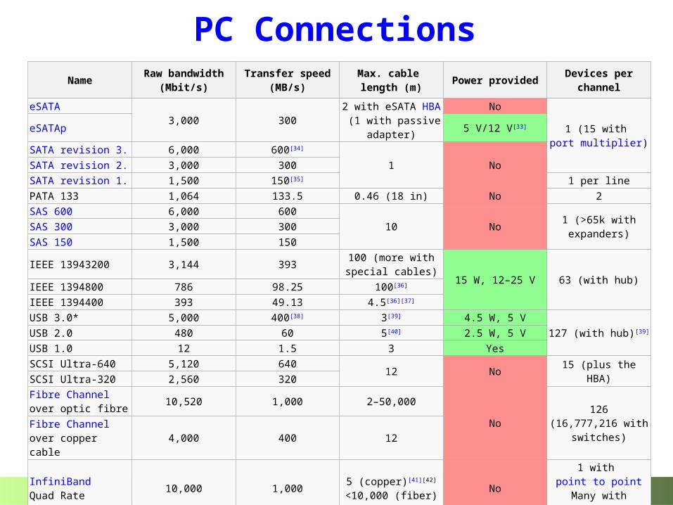
PC ConnectionsName
Raw bandwidth (Mbit/s)
Transfer speed (MB/s)
Max. cable length (m)
Power providedDevices per
channel
eSATA3,000 300
2 with eSATA HBA (1 with passive
adapter)
No
1 (15 with port multiplier)
eSATAp 5 V/12 V[33]
SATA revision 3.0 6,000 600[34]
1 NoSATA revision 2.0 3,000 300SATA revision 1.0 1,500 150[35] 1 per linePATA 133 1,064 133.5 0.46 (18 in) No 2SAS 600 6,000 600
10 No1 (>65k with expanders)
SAS 300 3,000 300SAS 150 1,500 150
IEEE 13943200 3,144 393100 (more with special cables)
15 W, 12–25 V 63 (with hub)IEEE 1394800 786 98.25 100[36]
IEEE 1394400 393 49.13 4.5[36][37]
USB 3.0* 5,000 400[38] 3[39] 4.5 W, 5 V127 (with hub)[39]USB 2.0 480 60 5[40] 2.5 W, 5 V
USB 1.0 12 1.5 3 YesSCSI Ultra-640 5,120 640
12 No 15 (plus the HBA)SCSI Ultra-320 2,560 320Fibre Channelover optic fibre
10,520 1,000 2–50,000No
126(16,777,216 with
switches)Fibre Channelover copper cable
4,000 400 12
InfiniBandQuad Rate
10,000 1,0005 (copper)[41][42]
<10,000 (fiber)No
1 with point to point
Many withswitched fabric
Thunderbolt 10,000 1,250 100 10 W 7