Composite Video Amplifier Output Capacitor-less Video...
17
1/16 www.rohm.com 2014.08 - Rev.B © 2009 ROHM Co., Ltd. All rights reserved. Composite Video Amplifier Output Capacitor-less Video Drivers BH76806FVM, BH76809FVM, BH76812FVM, BH76816FVM ●Description The BH768xxFVM series video drivers are the optimum solution for high density integration systems such as, digital still cameras, mobile phones, and portable video devices. A built-in charge pump circuit eliminates the need for a large output coupling capacitor. Features include: a built-in LPF, low-voltage (2.5 V) operation, and 0 μA current consumption during standby mode. ●Features 1) Select from four video driver amp gain settings: 6 dB, 9 dB, 12 dB, and 16.5 dB 2) Large-output video driver with maximum output voltage of 5.2 V P-P Supports wide and low-voltage operation range. 3) No output coupling capacitor is needed, which makes for a more compact design 4) Built-in standby function sets circuit current to 0 μA (typ.) during standby mode 5) Clear image reproduction by on-chip 8-order 4.5-MHz LPF (Low Pass Filter) 6) Bias input method is used to support chroma, video, and RGB signals. 7) MSOP8 compact package ●Applications Mobile telephones, DSCs (digital still cameras), DVCs (digital video cameras), portable game systems, portable media players, etc. ●Line up matrix Part No. Video driver amp gain Recommended input level BH76806FVM 6dB 1 V P-P BH76809FVM 9dB 0.7 V P-P BH76812FVM 12dB 0.5 V P-P BH76816FVM 16.5dB 0.3 V P-P ●Absolute maximum ratings (Ta=25℃) Parameter Symbol Ratings Unit Supply voltage VCC 3.55 V Power dissipation Pd 0.47 W Operating temperature range Topr -40 to +85 ℃ Storage temperature range Tstg -55 to +125 ℃ * Reduce by 4.7 mW/C over 25C, when mounted on a 70mm×70mm×1.6mm PCB board. No.14064EBT02
Transcript of Composite Video Amplifier Output Capacitor-less Video...

1/16 www.rohm.com 2014.08 - Rev.B
© 2009 ROHM Co., Ltd. All rights reserved.
Composite Video Amplifier Output Capacitor-less Video Drivers BH76806FVM, BH76809FVM, BH76812FVM, BH76816FVM
Description
The BH768xxFVM series video drivers are the optimum solution for high density integration systems such as, digital still cameras, mobile phones, and portable video devices. A built-in charge pump circuit eliminates the need for a large output coupling capacitor. Features include: a built-in LPF, low-voltage (2.5 V) operation, and 0 µA current consumption during standby mode.
Features
1) Select from four video driver amp gain settings: 6 dB, 9 dB, 12 dB, and 16.5 dB
2) Large-output video driver with maximum output voltage of 5.2 VP-P
Supports wide and low-voltage operation range.
3) No output coupling capacitor is needed, which makes for a more compact design
4) Built-in standby function sets circuit current to 0 µA (typ.) during standby mode
5) Clear image reproduction by on-chip 8-order 4.5-MHz LPF (Low Pass Filter)
6) Bias input method is used to support chroma, video, and RGB signals.
7) MSOP8 compact package Applications
Mobile telephones, DSCs (digital still cameras), DVCs (digital video cameras), portable game systems, portable media players, etc.
Line up matrix
Part No. Video driver amp gain Recommended input level
BH76806FVM 6dB 1 VP-P
BH76809FVM 9dB 0.7 VP-P
BH76812FVM 12dB 0.5 VP-P
BH76816FVM 16.5dB 0.3 VP-P
Absolute maximum ratings (Ta=25)
Parameter Symbol Ratings Unit
Supply voltage VCC 3.55 V
Power dissipation Pd 0.47 W
Operating temperature range Topr -40 to +85
Storage temperature range Tstg -55 to +125
* Reduce by 4.7 mW/C over 25C, when mounted on a 70mm×70mm×1.6mm PCB board.
No.14064EBT02
Technical Note
2/16
BH76806FVM, BH76809FVM, BH76812FVM, BH76816FVM
www.rohm.com 2014.08 - Rev.B© 2009 ROHM Co., Ltd. All rights reserved.
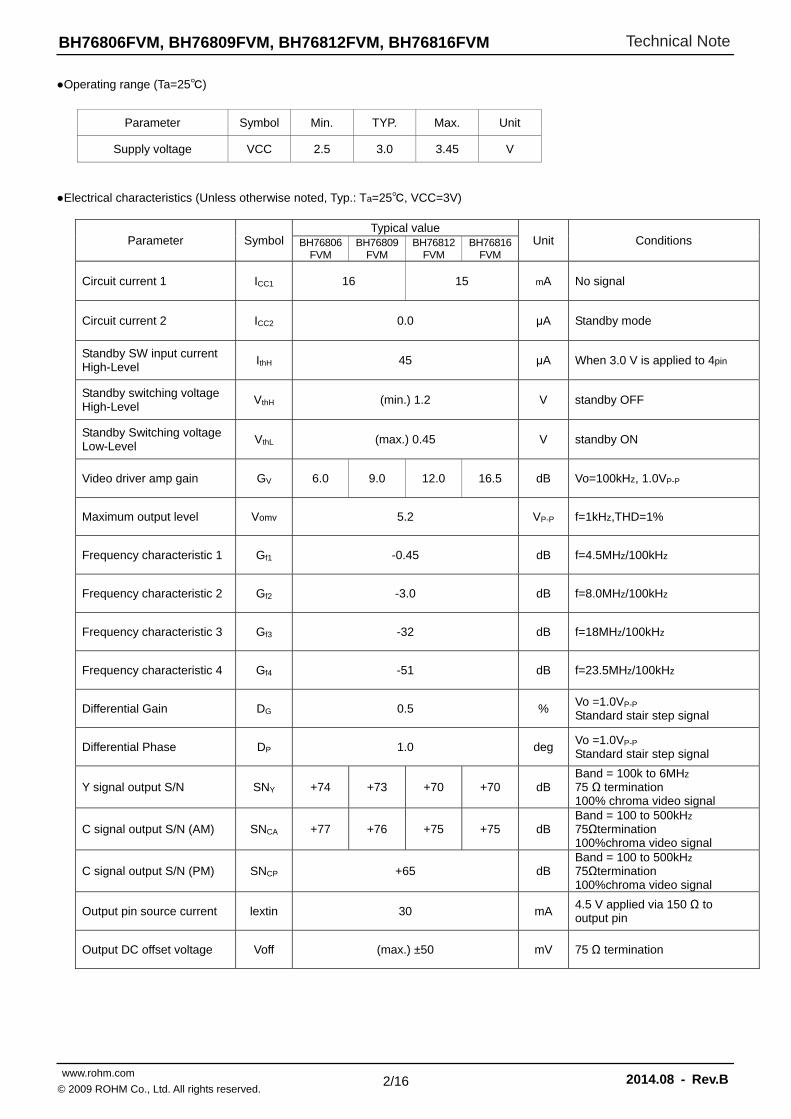
Operating range (Ta=25)
Parameter Symbol Min. TYP. Max. Unit
Supply voltage VCC 2.5 3.0 3.45 V
Electrical characteristics (Unless otherwise noted, Typ.: Ta=25, VCC=3V)
Parameter Symbol Typical value
Unit Conditions BH76806FVM
BH76809FVM
BH76812FVM
BH76816FVM
Circuit current 1 ICC1 16 15 mA No signal
Circuit current 2 ICC2 0.0 μA Standby mode
Standby SW input current High-Level
IthH 45 μA When 3.0 V is applied to 4pin
Standby switching voltage High-Level
VthH (min.) 1.2 V standby OFF
Standby Switching voltage Low-Level
VthL (max.) 0.45 V standby ON
Video driver amp gain GV 6.0 9.0 12.0 16.5 dB Vo=100kHz, 1.0VP-P
Maximum output level Vomv 5.2 VP-P f=1kHz,THD=1%
Frequency characteristic 1 Gf1 -0.45 dB f=4.5MHz/100kHz
Frequency characteristic 2 Gf2 -3.0 dB f=8.0MHz/100kHz
Frequency characteristic 3 Gf3 -32 dB f=18MHz/100kHz
Frequency characteristic 4 Gf4 -51 dB f=23.5MHz/100kHz
Differential Gain DG 0.5 % Vo =1.0VP-P Standard stair step signal
Differential Phase DP 1.0 deg Vo =1.0VP-P Standard stair step signal
Y signal output S/N SNY +74 +73 +70 +70 dB Band = 100k to 6MHz 75 Ω termination 100% chroma video signal
C signal output S/N (AM) SNCA +77 +76 +75 +75 dB Band = 100 to 500kHz 75Ωtermination 100%chroma video signal
C signal output S/N (PM) SNCP +65 dB Band = 100 to 500kHz 75Ωtermination 100%chroma video signal
Output pin source current lextin 30 mA 4.5 V applied via 150 Ω to output pin
Output DC offset voltage Voff (max.) ±50 mV 75 Ω termination
Technical Note
3/16
BH76806FVM, BH76809FVM, BH76812FVM, BH76816FVM
www.rohm.com 2014.08 - Rev.B© 2009 ROHM Co., Ltd. All rights reserved.
Measurement circuit
1
2
3
4
8
7
6
5
CHARGE PUMP
LPF
A
V
V0.1µ10µ
0.1µ
50
V4
OSC1
V2(VCC)
1
2
SW2
1µ
1µ
4.7µ75
75
6dB/9dB/12dB/16.5dB
NVCC
OUT
GND
150k
IN
+
-
Control pin settings
Parameter States Note
Standby control
STBY(4pin)=H STBY:OFF
STBY(4pin)=L STBY:ON
STBY(4pin)=OPEN STBY:ON
Block diagram
※ Test circuit is intended for shipment inspections, and differs from application circuit.
Fig. 1
Fig. 2
1
2
3
4
8
7
6
5
CHARGE PUMP
LPF6dB/9dB/12dB/16.5dB
NVCC
OUT
GND
150k
IN
C1
VCC
VIN
STBY
C2
NVCC
GND
VOUT
+
-
Technical Note
4/16
BH76806FVM, BH76809FVM, BH76812FVM, BH76816FVM
www.rohm.com 2014.08 - Rev.B© 2009 ROHM Co., Ltd. All rights reserved.
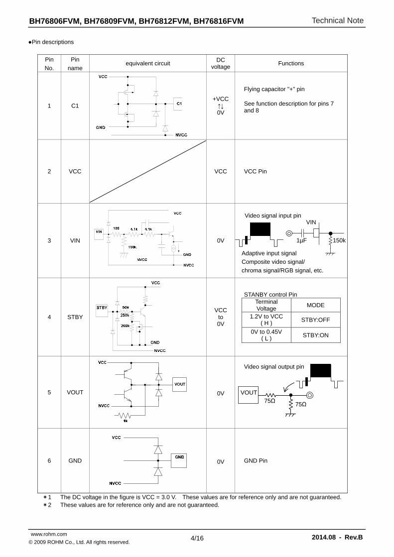
Pin descriptions
Pin
No.
Pin
name equivalent circuit
DC voltage
Functions
1 C1 +VCC ↑↓ 0V
Flying capacitor "+" pin
See function description for pins 7 and 8
2 VCC
VCC
VCC Pin
3 VIN 0V
Video signal input pin
4 STBY
VCC to 0V
STANBY control Pin Terminal Voltage
MODE
1.2V to VCC ( H ) STBY:OFF
0V to 0.45V ( L ) STBY:ON
5 VOUT 0V
Video signal output pin
6 GND
0V
GND Pin
*1 The DC voltage in the figure is VCC = 3.0 V. These values are for reference only and are not guaranteed. *2 These values are for reference only and are not guaranteed.
VIN
1µF 150k
Adaptive input signal
Composite video signal/
chroma signal/RGB signal, etc.
VOUT75Ω
75Ω
Technical Note
5/16
BH76806FVM, BH76809FVM, BH76812FVM, BH76816FVM
www.rohm.com 2014.08 - Rev.B© 2009 ROHM Co., Ltd. All rights reserved.
Pin descriptions
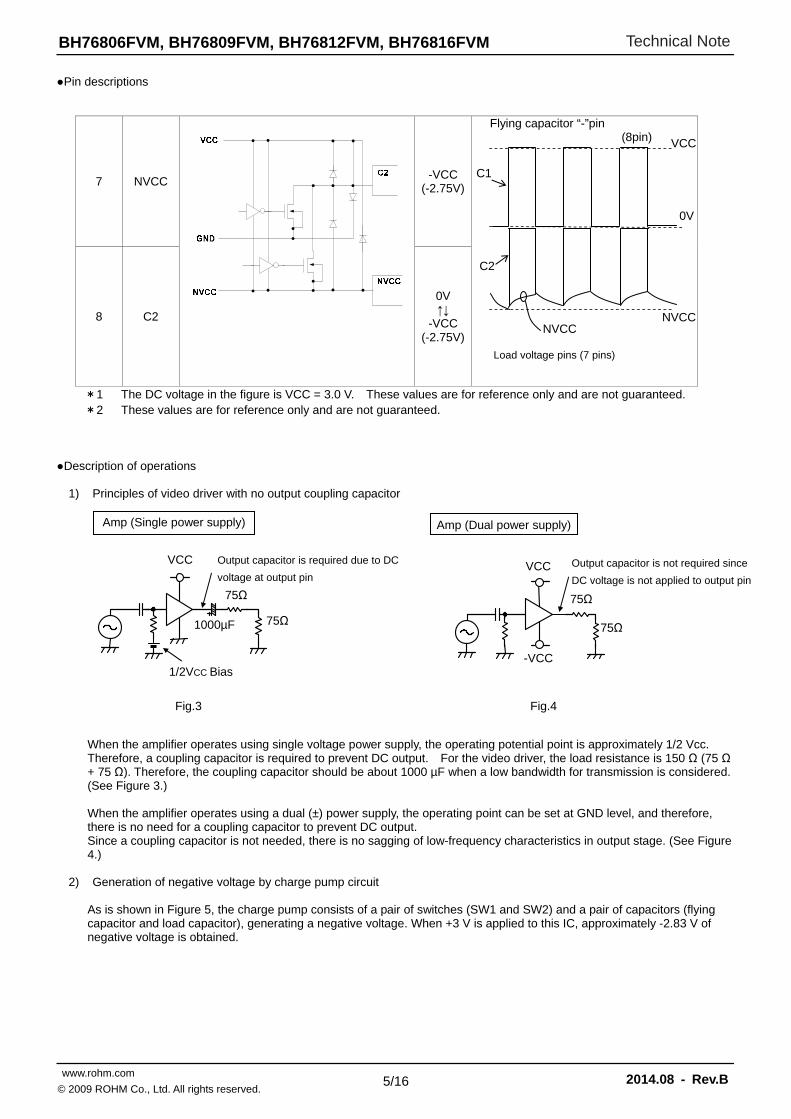
7 NVCC
-VCC (-2.75V)
Flying capacitor “-”pin (8pin)
8 C2
0V ↑↓
-VCC (-2.75V)
*1 The DC voltage in the figure is VCC = 3.0 V. These values are for reference only and are not guaranteed. *2 These values are for reference only and are not guaranteed.
Description of operations
1) Principles of video driver with no output coupling capacitor
When the amplifier operates using single voltage power supply, the operating potential point is approximately 1/2 Vcc. Therefore, a coupling capacitor is required to prevent DC output. For the video driver, the load resistance is 150 Ω (75 Ω + 75 Ω). Therefore, the coupling capacitor should be about 1000 µF when a low bandwidth for transmission is considered. (See Figure 3.)
When the amplifier operates using a dual (±) power supply, the operating point can be set at GND level, and therefore, there is no need for a coupling capacitor to prevent DC output. Since a coupling capacitor is not needed, there is no sagging of low-frequency characteristics in output stage. (See Figure 4.)
2) Generation of negative voltage by charge pump circuit
As is shown in Figure 5, the charge pump consists of a pair of switches (SW1 and SW2) and a pair of capacitors (flying capacitor and load capacitor), generating a negative voltage. When +3 V is applied to this IC, approximately -2.83 V of negative voltage is obtained.
0V
VCC
NVCC
C1
C2
NVCC
Load voltage pins (7 pins)
Amp (Dual power supply)
VCC
-VCC
75Ω
75Ω
Amp (Single power supply)
VCC
75Ω
75Ω
1/2VCC Bias
1000µF
Fig.3 Fig.4
Output capacitor is required due to DC
voltage at output pin Output capacitor is not required since
DC voltage is not applied to output pin
Technical Note
6/16
BH76806FVM, BH76809FVM, BH76812FVM, BH76816FVM
www.rohm.com 2014.08 - Rev.B© 2009 ROHM Co., Ltd. All rights reserved.
SW1 SW2
charge current
charge current
Flying capacitor
Load capacitor
Vcc +3V
SW1 SW2
charge current
Flying capacitor Load capacitor
Vcc +3V
Vcc +3Vcharge current
-Vcc is generated
-Vcc is generated
charge transfer mode
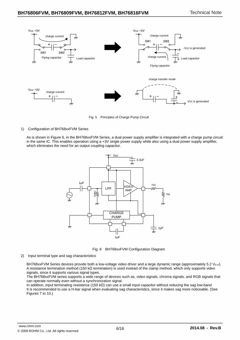
1) Configuration of BH768xxFVM Series
As is shown in Figure 6, in the BH768xxFVM Series, a dual power supply amplifier is integrated with a charge pump circuit in the same IC. This enables operation using a +3V single power supply while also using a dual power supply amplifier, which eliminates the need for an output coupling capacitor.
3.3uF
75Ω
75Ω
1µF
Vcc
1µF
1µF
CHARGE PUMP
LPFVIDEOAMP
2) Input terminal type and sag characteristics
BH768xxFVM Series devices provide both a low-voltage video driver and a large dynamic range (approximately 5.2 VP-P). A resistance termination method (150 kΩ termination) is used instead of the clamp method, which only supports video signals, since it supports various signal types. The BH768xxFVM series supports a wide range of devices such as, video signals, chroma signals, and RGB signals that can operate normally even without a synchronization signal. In addition, input terminating resistance (150 kΩ) can use a small input capacitor without reducing the sag low-band It is recommended to use a H-bar signal when evaluating sag characteristics, since it makes sag more noticeable. (See Figures 7 to 10.)
Fig. 5 Principles of Charge Pump Circuit
Fig. 6 BH768xxFVM Configuration Diagram

Technical Note
7/16
BH76806FVM, BH76809FVM, BH76812FVM, BH76816FVM
www.rohm.com 2014.08 - Rev.B© 2009 ROHM Co., Ltd. All rights reserved.
a) Sag-free TV Test Signal Generator Output(Sibasoku TG-7/1 , H-bar)
b) BH768xxFVM output (input = 1.0 µF, output, H-bar)
c) 1000 µF + 150 Ω sag waveform (TV Test Signal Generator Sibasoku TG-7/1 output, H-bar)
Fig. 7
1µF
150k
Sag
Sag is determined by input capacitor and input resistance only.
Cut-off frequency for input capacitor and input impedance is the same as when the output capacitor is set at 1000 µF with an ordinary 75 Ω driver.
1 μF X 150 KΩ = 1000 μF X 150 Ω (Input terminal time constant) (Output terminal time constant)
H-bar signal's TV screen output image
75Ω
75Ω
Monitor 1μF
TG-7/1
BH768xxFVM
Nearly identical sag characteristics
Fig. 8
Fig. 9
Fig. 10
150k
TG-7/1
75Ω
75Ω
Monitor
1000μF
VCC
-VCC
Technical Note
8/16
BH76806FVM, BH76809FVM, BH76812FVM, BH76816FVM
www.rohm.com 2014.08 - Rev.B© 2009 ROHM Co., Ltd. All rights reserved.
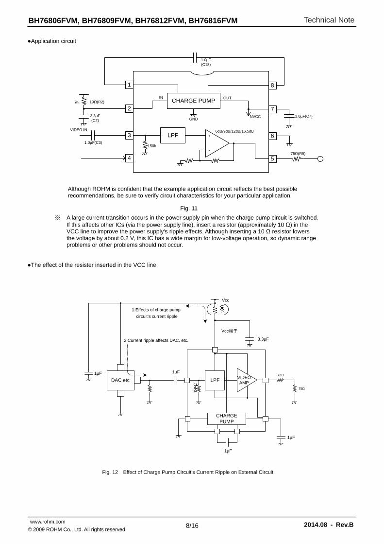
Application circuit
1
2
3
4
8
7
6
5
CHARGE PUMP
LPF
1.0µF(C18)
1.0µF(C7)
75Ω(R5)
6dB/9dB/12dB/16.5dB
NVCC
OUT
GND
150k
IN
3.3µF(C2)
10Ω(R2)※
1.0µF(C3)
VIDEO IN
+
-
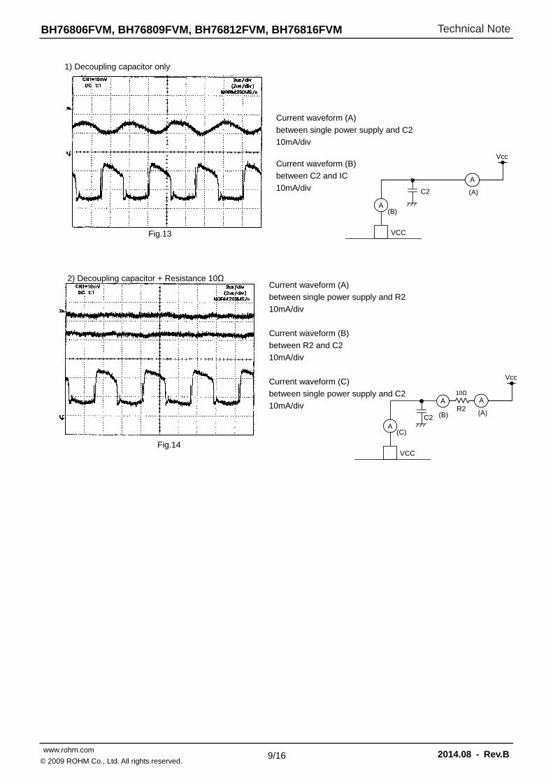
※ A large current transition occurs in the power supply pin when the charge pump circuit is switched. If this affects other ICs (via the power supply line), insert a resistor (approximately 10 Ω) in the VCC line to improve the power supply's ripple effects. Although inserting a 10 Ω resistor lowers the voltage by about 0.2 V, this IC has a wide margin for low-voltage operation, so dynamic range problems or other problems should not occur. The effect of the resister inserted in the VCC line
1.Effects of charge pump
circuit’s current ripple
2.Current ripple affects DAC, etc.
DAC etc
3.3µF
Vcc端子
Vcc
1µF 75Ω
75Ω
CHARGE PUMP
1µF
1µF
1µF
LPFVIDEOAMP
Although ROHM is confident that the example application circuit reflects the best possible recommendations, be sure to verify circuit characteristics for your particular application.
Fig. 12 Effect of Charge Pump Circuit's Current Ripple on External Circuit
Fig. 11
Technical Note
9/16
BH76806FVM, BH76809FVM, BH76812FVM, BH76816FVM
www.rohm.com 2014.08 - Rev.B© 2009 ROHM Co., Ltd. All rights reserved.
1) Decoupling capacitor only
2) Decoupling capacitor + Resistance 10Ω
Current waveform (A)
between single power supply and C2
10mA/div Current waveform (B)
between C2 and IC
10mA/div
Current waveform (A)
between single power supply and R2
10mA/div
Current waveform (B)
between R2 and C2
10mA/div
Current waveform (C)
between single power supply and C2
10mA/div
Fig.13
Fig.14
A(B)
Vcc
(A)
A
VCC
C2
A
A
Vcc
10ΩA
VCC
C2R2
(C)
(A)(B)
Technical Note
10/16
BH76806FVM, BH76809FVM, BH76812FVM, BH76816FVM
www.rohm.com 2014.08 - Rev.B© 2009 ROHM Co., Ltd. All rights reserved.
Pattern diagram of evaluation board List of external components
Symbol Function Recommended
value Remark
C1 Flying capacitor 1μF B characteristics are recommended
C2 Tank capacitor 1μF B characteristics are recommended
C3 Input coupling capacitor 1μF B characteristics are recommended
C4 Decoupling capacitor 3.3μF B characteristics are recommended
R1 Output resistor 75Ω -
R2 Output terminating resistance 75Ω Not required when connecting to TV or video signal test equipment.
R3 Input terminating resistance 75Ω Required when connecting to video signal test equipment.
CN1 Input connector BNC
CN2 Output connector RCA (pin jack)
SW STBY control SW
GND
GND GND
GND
GND
GND
GNDVCC C1
C2
C3
C4
STBY
ROHM BH76806/09/12/16FVM
R3
R1
R2
ACT
VIN VOUT
Fig. 15
CN1 CN2
SW
Technical Note
11/16
BH76806FVM, BH76809FVM, BH76812FVM, BH76816FVM
www.rohm.com 2014.08 - Rev.B© 2009 ROHM Co., Ltd. All rights reserved.
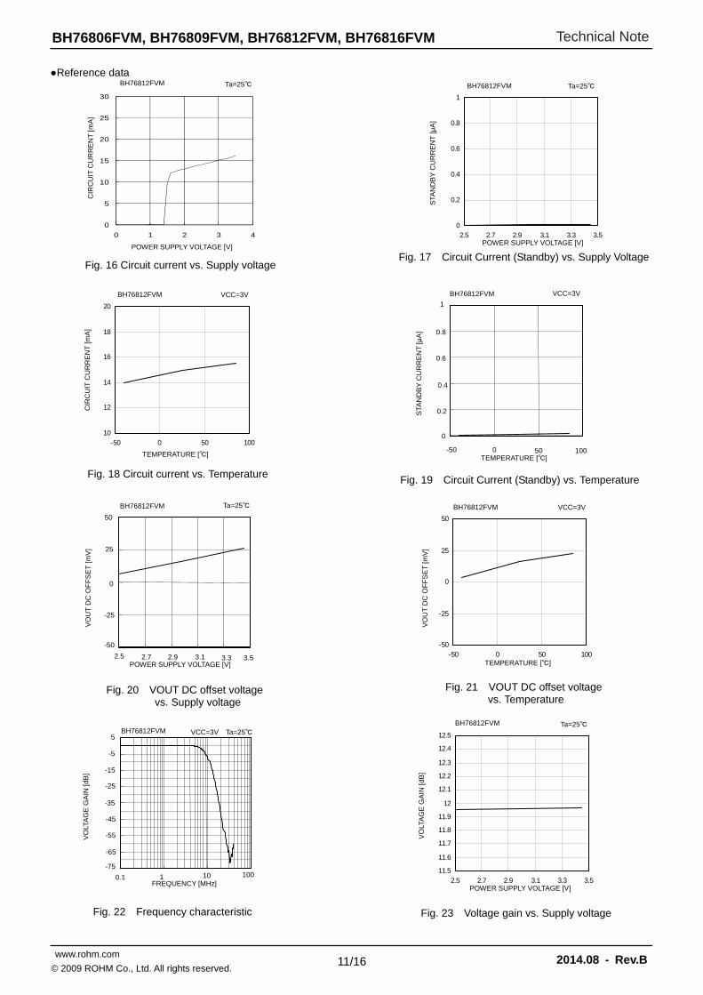
Reference data
Fig. 16 Circuit current vs. Supply voltage
Fig. 18 Circuit current vs. Temperature Fig. 19 Circuit Current (Standby) vs. Temperature
Fig. 20 VOUT DC offset voltage vs. Supply voltage
Fig. 21 VOUT DC offset voltage vs. Temperature
Fig. 22 Frequency characteristic Fig. 23 Voltage gain vs. Supply voltage
POWER SUPPLY VOLTAGE [V]
CIR
CU
IT C
UR
RE
NT
[m
A]
Ta=25
10
12
14
16
18
20
-50 0 50 100
CIR
CU
IT C
UR
RE
NT
[m
A]
TEMPERATURE []
VCC=3V
-50
-25
0
25
50
-50 0 50 100TEMPERATURE []
VO
UT
DC
OF
FS
ET
[m
V]
VCC=3V
0
0.2
0.4
0.6
0.8
1
2.5 2.7 2.9 3.1 3.3 3.5
STA
ND
BY
CU
RR
EN
T [μ
A]
POWER SUPPLY VOLTAGE [V]
Ta=25
11.5
11.6
11.7
11.8
11.9
12
12.1
12.2
12.3
12.4
12.5
2.5 2.7 2.9 3.1 3.3 3.5
VO
LTA
GE
GA
IN [d
B]
POWER SUPPLY VOLTAGE [V]
Ta=25
0
0.2
0.4
0.6
0.8
1
-50 0 50 100
VCC=3V
TEMPERATURE []
STA
ND
BY
CU
RR
EN
T [μ
A]
-50
-25
0
25
50
2.5 2.7 2.9 3.1 3.3 3.5
VO
UT
DC
OF
FS
ET
[m
V]
Ta=25
POWER SUPPLY VOLTAGE [V]
-75
-65
-55
-45
-35
-25
-15
-5
5
0.1 1 10 100
VO
LTA
GE
GA
IN [d
B]
FREQUENCY [MHz]
VCC=3V Ta=25
BH76812FVM BH76812FVM
BH76812FVM BH76812FVM
BH76812FVM BH76812FVM
BH76812FVM BH76812FVM
Fig. 17 Circuit Current (Standby) vs. Supply Voltage
0
5
10
15
20
25
30
0 1 2 3 4
Technical Note
12/16
BH76806FVM, BH76809FVM, BH76812FVM, BH76816FVM
www.rohm.com 2014.08 - Rev.B© 2009 ROHM Co., Ltd. All rights reserved.
-1
-0.8
-0.6
-0.4
-0.2
0
0.2
0.4
0.6
0.8
1
2.5 2.7 2.9 3.1 3.3 3.5
POWER SUPPLY VOLTAGE:Vcc[V]
FR
EQ
EN
CY
RE
SP
ON
SE
1:G
f1[d
B]
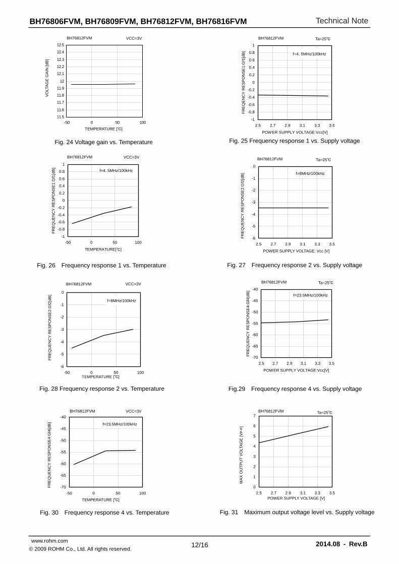
Fig. 24 Voltage gain vs. Temperature Fig. 25 Frequency response 1 vs. Supply voltage
Fig. 26 Frequency response 1 vs. Temperature Fig. 27 Frequency response 2 vs. Supply voltage
Fig. 28 Frequency response 2 vs. Temperature Fig.29 Frequency response 4 vs. Supply voltage
Fig. 30 Frequency response 4 vs. Temperature Fig. 31 Maximum output voltage level vs. Supply voltage
11.5
11.6
11.7
11.8
11.9
12
12.1
12.2
12.3
12.4
12.5
-50 0 50 100
TEMPERATURE []
VO
LTA
GE
GA
IN [d
B]
VCC=3V
-6
-5
-4
-3
-2
-1
0
-50 0 50 100TEMPERATURE []
FR
EQ
UE
NC
Y R
ES
PO
NS
E2
:Gf2
[dB
]
VCC=3V
TEMPERATURE [Deg]
-70
-65
-60
-55
-50
-45
-40
-50 0 50 100
FR
EQ
UE
NC
Y R
ES
PO
NS
E4
:Gf4
[dB
]
VCC=3V
Ta=25
POWER SUPPLY VOLTAGE [V]
0
1
2
3
4
5
6
7
2.5 2.7 2.9 3.1 3.3 3.5
MA
X O
UT
PU
T V
OLT
AG
E [
VP
-P]
Ta=25
-6
-5
-4
-3
-2
-1
0
2.5 2.7 2.9 3.1 3.3 3.5F
RE
QU
EN
CY
RE
SP
ON
SE
2:G
f2[d
B]
Ta=25
POWER SUPPLY VOLTAGE: Vcc [V]
BH76812FVM
BH76812FVM
BH76812FVM
-1
-0.8
-0.6
-0.4
-0.2
0
0.2
0.4
0.6
0.8
1
-50 0 50 100
TEMPERATURE[]
FR
EQ
UE
NC
Y R
ES
PO
NS
E1:
Gf1
[dB
]
-70
-65
-60
-55
-50
-45
-40
2.5 2.7 2.9 3.1 3.3 3.5
POWER SUPPLY VOLTAGE:Vcc[V]
FR
EQ
UE
NC
Y R
ES
PO
NS
E4:
Gf4
[dB
]
VCC=3V BH76812FVM BH76812FVM
BH76812FVM Ta=25 BH76812FVM
BH76812FVM
f=8MHz/100kHz
f=23.5MHz/100kHz
f=23.5MHz/100kHz
f=8MHz/100kHz
f=4. 5MHz/100kHz
f=4. 5MHz/100kHz
TEMPERATURE []
Technical Note
13/16
BH76806FVM, BH76809FVM, BH76812FVM, BH76816FVM
www.rohm.com 2014.08 - Rev.B© 2009 ROHM Co., Ltd. All rights reserved.
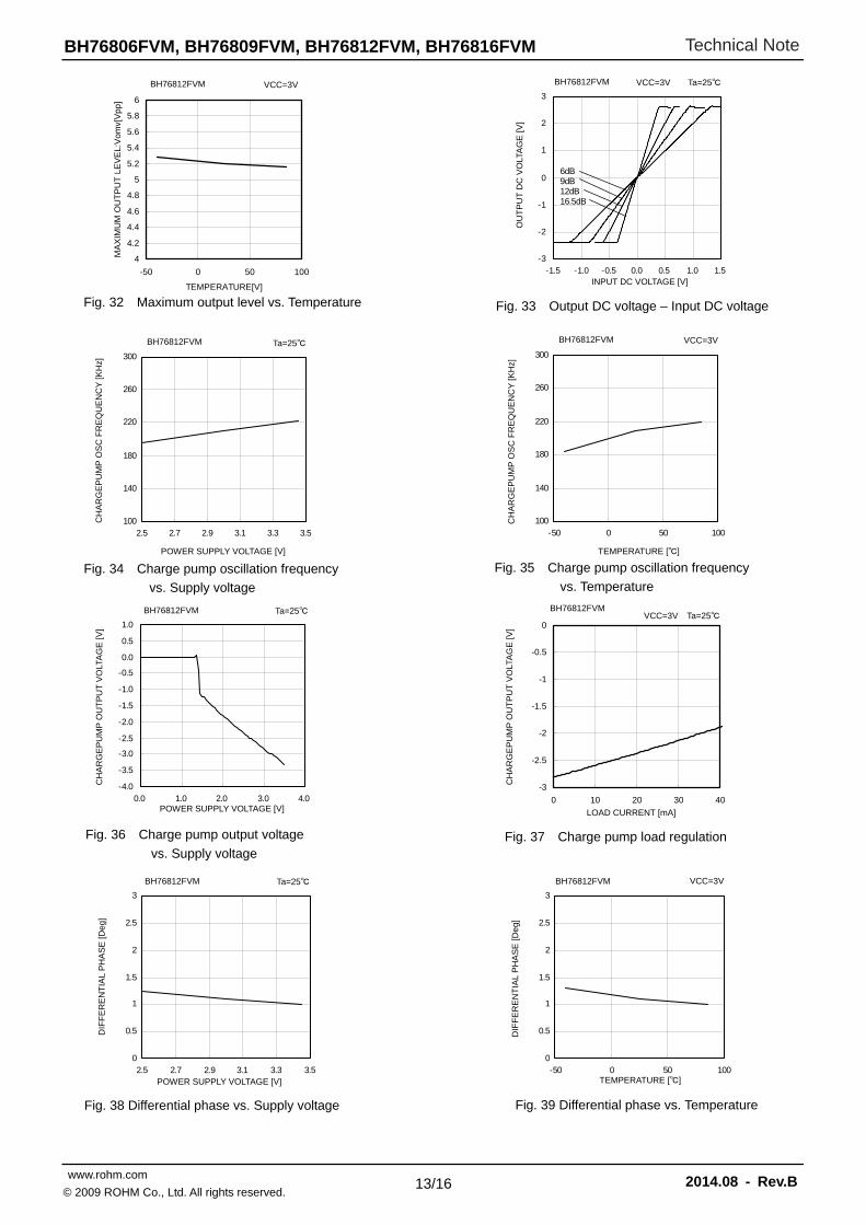
Fig. 37 Charge pump load regulation
Fig. 39 Differential phase vs. Temperature
Fig. 33 Output DC voltage – Input DC voltage
Fig. 34 Charge pump oscillation frequency
vs. Supply voltage
Fig. 36 Charge pump output voltage
vs. Supply voltage
Fig. 38 Differential phase vs. Supply voltage
-3
-2.5
-2
-1.5
-1
-0.5
0
0 10 20 30 40
LOAD CURRENT [mA]
CH
AR
GE
PU
MP
OU
TP
UT
VO
LTA
GE
[V]
VCC=3V Ta=25
100
140
180
220
260
300
-50 0 50 100
TEMPERATURE []
CH
AR
GE
PU
MP
OS
C F
RE
QU
EN
CY
[KH
z]
VCC=3V
0
0.5
1
1.5
2
2.5
3
-50 0 50 100TEMPERATURE []
DIF
FE
RE
NT
IAL
PH
AS
E [D
eg]
VCC=3V
100
140
180
220
260
300
2.5 2.7 2.9 3.1 3.3 3.5
POWER SUPPLY VOLTAGE [V]
CH
AR
GE
PU
MP
OS
C F
RE
QU
EN
CY
[KH
z]
Ta=25
-4.0
-3.5
-3.0
-2.5
-2.0
-1.5
-1.0
-0.5
0.0
0.5
1.0
0.0 1.0 2.0 3.0 4.0POWER SUPPLY VOLTAGE [V]
CH
AR
GE
PU
MP
OU
TP
UT
VO
LTA
GE
[V]
Ta=25
0
0.5
1
1.5
2
2.5
3
2.5 2.7 2.9 3.1 3.3 3.5POWER SUPPLY VOLTAGE [V]
DIF
FE
RE
NT
IAL
PH
AS
E [D
eg]
Ta=25
-3
-2
-1
0
1
2
3
-1.5 -1.0 -0.5 0.0 0.5 1.0 1.5INPUT DC VOLTAGE [V]
OU
TP
UT
DC
VO
LTA
GE
[V
]
VCC=3V Ta=25
6dB 9dB 12dB 16.5dB
4
4.2
4.4
4.6
4.8
5
5.2
5.4
5.6
5.8
6
-50 0 50 100
TEMPERATURE[V]
MA
XIM
UM
OU
TP
UT
LE
VE
L:V
om
v[V
pp
]
Fig. 32 Maximum output level vs. Temperature
BH76812FVM VCC=3V BH76812FVM
BH76812FVM BH76812FVM
BH76812FVM BH76812FVM
BH76812FVM BH76812FVM
Fig. 35 Charge pump oscillation frequency
vs. Temperature
Technical Note
14/16
BH76806FVM, BH76809FVM, BH76812FVM, BH76816FVM
www.rohm.com 2014.08 - Rev.B© 2009 ROHM Co., Ltd. All rights reserved.
50
52
54
56
58
60
62
64
66
68
70
2.5 2.7 2.9 3.1 3.3 3.5
POWER SUPPLY VOLTAGE: Vcc[V]
C S
YS
TE
M P
M S
/N:S
Ncp
[dB
]
Fig. 44 S/N(C-AM) vs. Supply Voltage Fig. 45 S/N(C-AM) vs. Temperature
Fig. 40 Differential gain vs. Supply voltage Fig. 41 Differential gain vs. Temperature
Fig. 42 S/N(Y) vs. Supply Voltage
Fig. 46 S/N(C-PM) vs. Supply Voltage Fig. 47 S/N(C-PM) vs. Temperature
Fig.43 S/N(Y) vs. Temperature
0
0.5
1
1.5
2
2.5
3
-50 0 50 100TEMPERATURE []
DIF
FE
RE
NT
IAL
GA
IN [%
]
VCC=3V
60
65
70
75
80
-50 0 50 100
TEMPERATURE []
Y
S/N
[dB
]
VCC=3V
60
65
70
75
80
-50 0 50 100TEMPERATURE []
CH
RO
MA
S/N
(A
M)
[dB
]
VCC=3V
50
55
60
65
70
-50 0 50 100
CH
RO
MA
S/N
(P
M)
[dB
]
TEMPERATURE []
VCC=3V
0
0.5
1
1.5
2
2.5
3
2.5 2.7 2.9 3.1 3.3 3.5POWER SUPPLY VOLTAGE [V]
DIF
FE
RE
NT
IAL
GA
IN [%
]
Ta=25
60
65
70
75
80
2.5 2.7 2.9 3.1 3.3 3.5POWER SUPPLY VOLTAGE [V]
Y
S/N
[dB
]
Ta=25
60
65
70
75
80
2.5 2.7 2.9 3.1 3.3 3.5POWER SUPPLY VOLTAGE [V]
CH
RO
MA
S/N
(A
M)
[dB
]
Ta=25
Ta=25
BH76812FVM BH76812FVM
BH76812FVM BH76812FVM
BH76812FVM
BH76812FVM
BH76812FVM
BH76812FVM

Technical Note
15/16
BH76806FVM, BH76809FVM, BH76812FVM, BH76816FVM
www.rohm.com 2014.08 - Rev.B© 2009 ROHM Co., Ltd. All rights reserved.
Cautions on use
1. Numbers and data in entries are representative design values and are not guaranteed values of the items.
2. Although ROHM is confident that the example application circuit reflects the best possible recommendations, be sure
to verify circuit characteristics for your particular application. Modification of constants for other externally connected
circuits may cause variations in both static and transient characteristics for external components as well as this Rohm
IC. Allow for sufficient margins when determining circuit constants.
3. Absolute maximum ratings
Use of the IC in excess of absolute maximum ratings, such as the applied voltage or operating temperature range
(Topr), may result in IC damage. Assumptions should not be made regarding the state of the IC (short mode or
open mode) when such damage is suffered. A physical safety measure, such as a fuse, should be implemented
when using the IC at times where the absolute maximum ratings may be exceeded.
4. Thermal design
Perform thermal design, in which there are adequate margins, by taking into account the permissible dissipation
(Pd) in actual states of use.
5. Short circuit between terminals and erroneous mounting
Pay attention to the assembly direction of the ICs. Wrong mounting direction or shorts between terminals, GND, or other
components on the circuits, can damage the IC.
6. Operation in strong electromagnetic field
Using the ICs in a strong electromagnetic field can cause operation malfunction.
7. Wiring from the decoupling capacitor C2 to the IC should be kept as short as possible.
This capacitance value may have ripple effects on the IC, and may affect the S-N ratio. It is recommended to use
as large a decoupling capacitor as possible. (Recommendations: 3.3 µF, B characteristics, 6.3 V or higher)
8. Target capacitor
It is recommended to use a ceramic capacitor with good temperature characteristics (B).
9. The NVCC (7 pin) terminal generates a voltage that is used within the IC, so it should not be connected to a load
unless necessary. This capacitor (C7) has a large capacitance value with low negative voltage ripple.
10. Capacitors C18 and C2 should be placed as close as possible to the IC. If the wire length to the capacitor is too
long, it can lead to switching noise. (Recommended C18: 1.0 µF; C2: 3.3 µF, B characteristics, 6.3 V or higher
maximum voltage)
11. The HPF consists of input coupling capacitor C3 and 150 kΩ of the internal input.
Be sure to check for video signal sag before determining the C3 value.
The cut-off frequency fc can be calculated using the following formula.
fc = 1/(2π× C3 × 150 kΩ) (Recommendations: 1.0 µF, B characteristics, 6.3 V or higher maximum voltage)
12. The output resistor R5 should be placed close to the IC.
13. Improper mounting may damage the IC.
14. A large current transition occurs in the power supply pin when the charge pump circuit is switched. If this affects
other ICs (via the power supply line), insert a resistor (approximately 10 Ω) in the VCC line to improve the power
supply's ripple effects. Although inserting a 10 Ω resistor lowers the voltage by about 0.2 V, this IC has a wide margin
for low-voltage operation, so dynamic range problems or other problems should not occur. (See Figures 12 to 14.)
0
5
10
15
20
0.0 0.5 1.0 1.5 2.0
Fig. 48 Circuit current vs. STBY terminal voltage
STBY TERMINAL VOLTAGE [V]
CIR
CU
IT C
UR
RE
NT
[m
A]
VCC=3V Ta=25 BH76812FVM
Technical Note
16/16
BH76806FVM, BH76809FVM, BH76812FVM, BH76816FVM
www.rohm.com 2014.08 - Rev.B© 2009 ROHM Co., Ltd. All rights reserved.
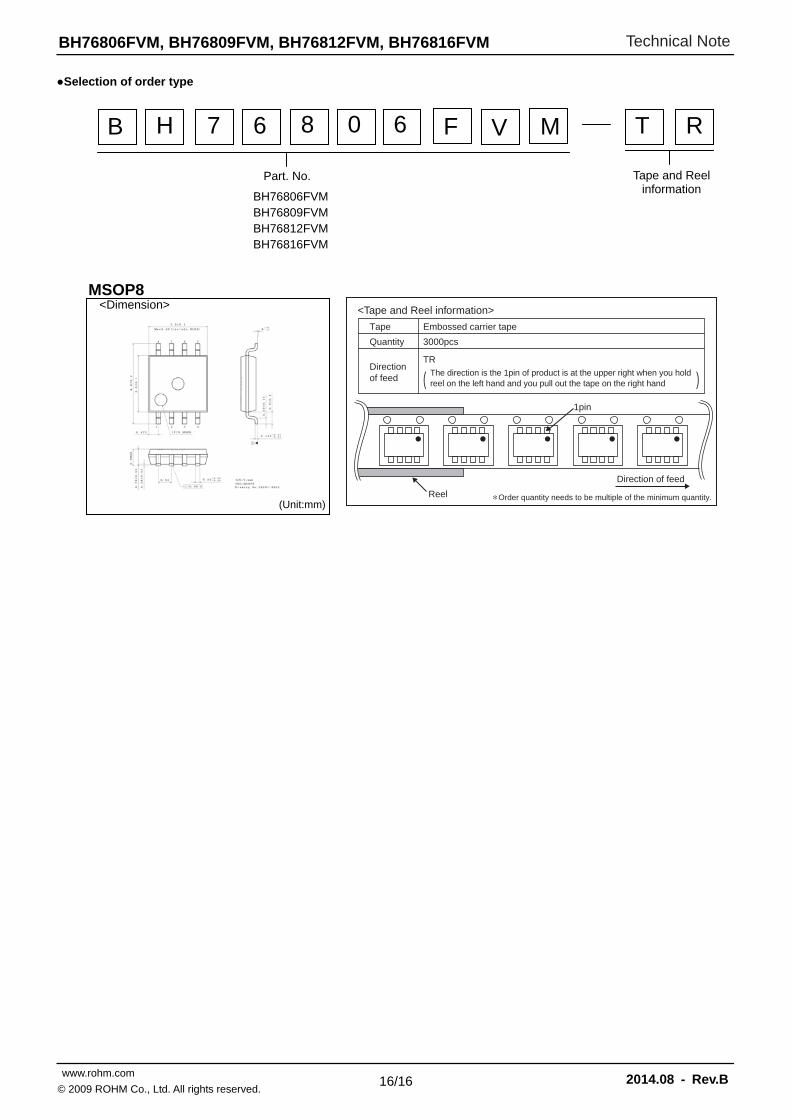
Selection of order type
B H 7 6 8 0 T R
Part. No.
F
Tape and Reelinformation
V M
BH76806FVM BH76809FVMBH76812FVMBH76816FVM
6
Direction of feed
Reel ∗ Order quantity needs to be multiple of the minimum quantity.
<Tape and Reel information>
Embossed carrier tapeTape
Quantity
Direction of feed
The direction is the 1pin of product is at the upper right when you hold reel on the left hand and you pull out the tape on the right hand
3000pcs
TR
( )1pin
MSOP8 <Dimension>
(Unit:mm)
R1102Awww.rohm.com© 2014 ROHM Co., Ltd. All rights reserved.
Notice
ROHM Customer Support System http://www.rohm.com/contact/
Thank you for your accessing to ROHM product informations. More detail product informations and catalogs are available, please contact us.
N o t e s
The information contained herein is subject to change without notice.
Before you use our Products, please contact our sales representative and verify the latest specifica-tions :
Although ROHM is continuously working to improve product reliability and quality, semicon-ductors can break down and malfunction due to various factors.Therefore, in order to prevent personal injury or fire arising from failure, please take safety measures such as complying with the derating characteristics, implementing redundant and fire prevention designs, and utilizing backups and fail-safe procedures. ROHM shall have no responsibility for any damages arising out of the use of our Poducts beyond the rating specified by ROHM.
Examples of application circuits, circuit constants and any other information contained herein are provided only to illustrate the standard usage and operations of the Products. The peripheral conditions must be taken into account when designing circuits for mass production.
The technical information specified herein is intended only to show the typical functions of and examples of application circuits for the Products. ROHM does not grant you, explicitly or implicitly, any license to use or exercise intellectual property or other rights held by ROHM or any other parties. ROHM shall have no responsibility whatsoever for any dispute arising out of the use of such technical information.
The Products are intended for use in general electronic equipment (i.e. AV/OA devices, communi-cation, consumer systems, gaming/entertainment sets) as well as the applications indicated in this document.
The Products specified in this document are not designed to be radiation tolerant.
For use of our Products in applications requiring a high degree of reliability (as exemplified below), please contact and consult with a ROHM representative : transportation equipment (i.e. cars, ships, trains), primary communication equipment, traffic lights, fire/crime prevention, safety equipment, medical systems, servers, solar cells, and power transmission systems.
Do not use our Products in applications requiring extremely high reliability, such as aerospace equipment, nuclear power control systems, and submarine repeaters.
ROHM shall have no responsibility for any damages or injury arising from non-compliance with the recommended usage conditions and specifications contained herein.
ROHM has used reasonable care to ensur the accuracy of the information contained in this document. However, ROHM does not warrants that such information is error-free, and ROHM shall have no responsibility for any damages arising from any inaccuracy or misprint of such information.
Please use the Products in accordance with any applicable environmental laws and regulations, such as the RoHS Directive. For more details, including RoHS compatibility, please contact a ROHM sales office. ROHM shall have no responsibility for any damages or losses resulting non-compliance with any applicable laws or regulations.
When providing our Products and technologies contained in this document to other countries, you must abide by the procedures and provisions stipulated in all applicable export laws and regulations, including without limitation the US Export Administration Regulations and the Foreign Exchange and Foreign Trade Act.
This document, in part or in whole, may not be reprinted or reproduced without prior consent of ROHM.
1)
2)
3)
4)
5)
6)
7)
8)
9)
10)
11)
12)
13)
14)