
Complete ICA Manual as on 23-10-2013
61
IC Applications Lab PART-1 Department of ECE Sreyas Institute of Engineering & Technology
description
IC Application lab manual for III B.Tech ECE
Transcript of Complete ICA Manual as on 23-10-2013
IC Applications Lab
PART-1
Department of ECE Sreyas Institute of Engineering & Technology
IC Applications Lab
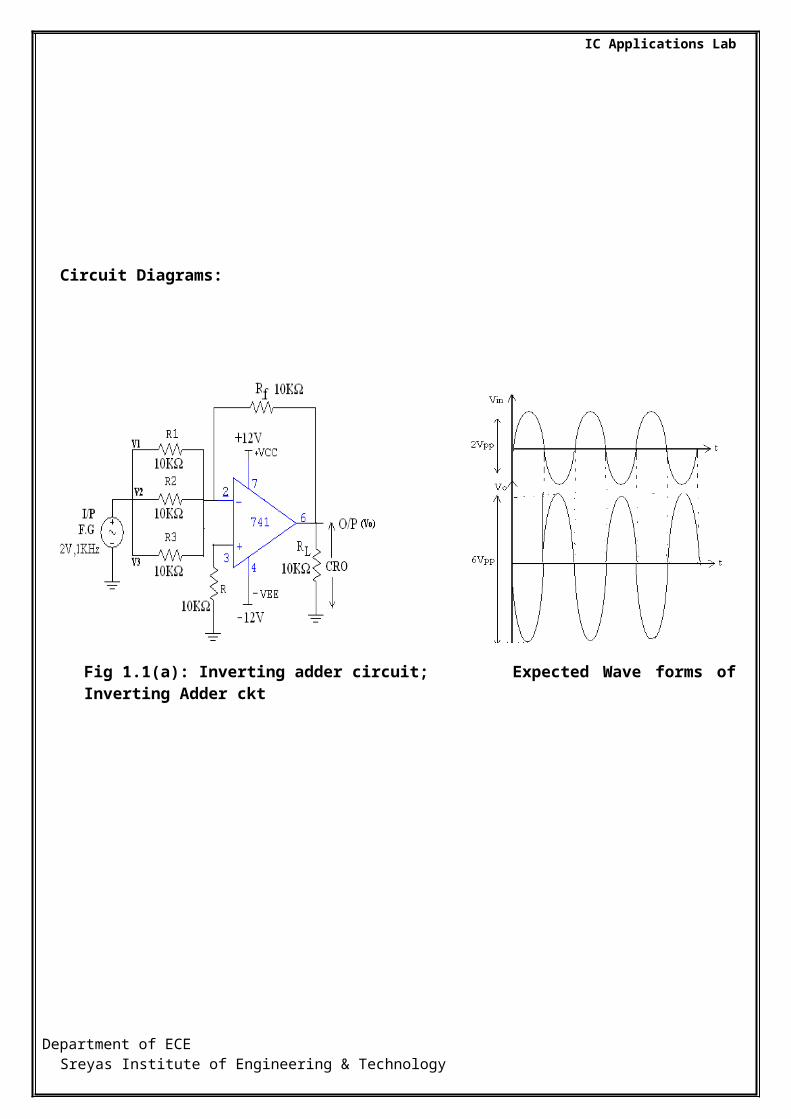
Circuit Diagrams:
Fig 1.1(a): Inverting adder circuit; Expected Wave forms of Inverting Adder ckt
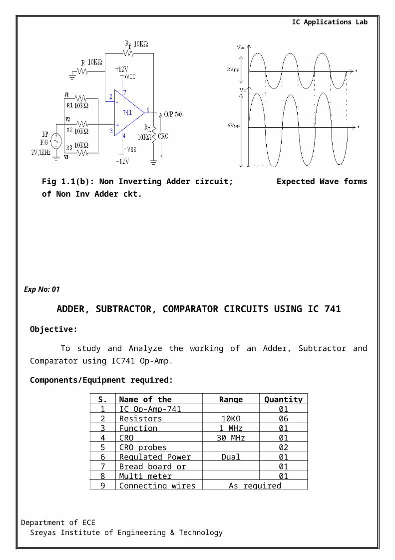
Fig 1.1(b): Non Inverting Adder circuit; Expected Wave forms of Non Inv Adder ckt.
Department of ECE Sreyas Institute of Engineering & Technology
IC Applications Lab
Exp No: 01
ADDER, SUBTRACTOR, COMPARATOR CIRCUITS USING IC 741
Objective:
To study and Analyze the working of an Adder, Subtractor and Comparator using IC741 Op-Amp.
Components/Equipment required:
S. No Name of the Apparatus Range Quantity1 IC Op-Amp-741 012 Resistors 10KΩ 063 Function Generator 1 MHz 014 CRO 30 MHz 015 CRO probes 026 Regulated Power Supply Dual channel 017 Bread board or trainer
kit01
8 Multi meter 019 Connecting wires As required
Theory:
(PLEASE REFER CLASS NOTES / STANDARD TEXT BOOK
WHILE WRITING IN RECORD)
Introduction:
When the input signal to an op-amp is supplied to the inverting input with non-inverting input at ground, the amplifier operates in the inverting mode that is the output differs in phase by 180 degrees with respect to the input. In an inverting amplifier the gain is given by the relation A = - (Rf/R1) . Where RF and R1 are the feedback and input resistor respectively. When operated in the non-inverting mode, the input signal is applied to the non-inverting input with the inverting terminal grounded through a resistor. The gain in this case is given by the relation A = 1+ (Rf/R1)
Adder:
Summing amplifier is a circuit whose output is the sum of several input signals. For example, an inverting summing amplifier with two inputs v1, v2, two input resistors R1, R2 and a feedback resistor Rf and output vo as follows
Vo= -R f(V1/R1+V2/R2)Vo is the inverted sum of three input signals if Rf=R1=R2
Vo= - (V1+V2)Non-inverting summing amplifier for the same configuration
Vo= (1+Rf/R)(V1/R1+V2/R2)/(1/R1+1/R2)If Rf= R=R1=R2 Then Vo= V1+V2.
Department of ECE Sreyas Institute of Engineering & Technology

IC Applications Lab
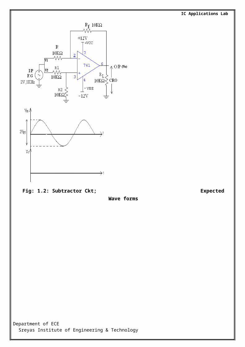
Fig: 1.2: Subtractor Ckt; Expected Wave forms
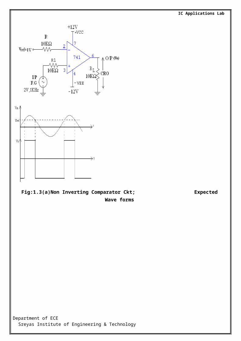
Fig:1.3(a)Non Inverting Comparator Ckt; Expected Wave forms
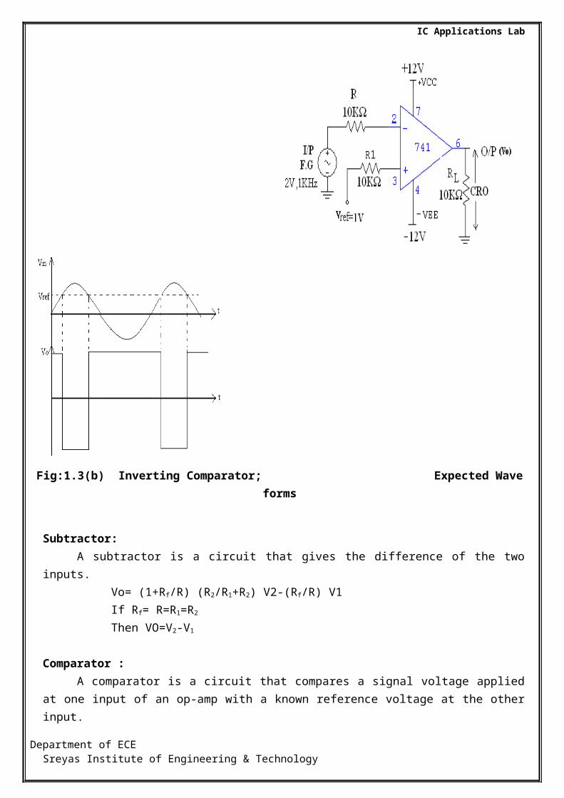
Fig:1.3(b) Inverting Comparator; Expected Wave forms
Department of ECE Sreyas Institute of Engineering & Technology
IC Applications Lab
Subtractor:A subtractor is a circuit that gives the difference of the two inputs.
Vo= (1+Rf/R) (R2/R1+R2) V2-(Rf/R) V1If Rf= R=R1=R2
Then VO=V2-V1
Comparator :A comparator is a circuit that compares a signal voltage applied at one input of an op-amp with a
known reference voltage at the other input.
Procedure:
Adder:1. Connect the Adder circuit as shown in figure 1.1(a) & 1.1(b).2. Apply the input sine wave to the Inverting/Non-Inverting Input of op-amp through resistors R1,
R2 & R3. 3. Verify the output at the 6th pin. 4. Apply different input voltages and tabulate the results in the tabular form.5. Plot the graph of the output of adder circuit. .
Subtractor: 1. Connect the Subtractor circuit as shown in figure 1.2.2. Apply the input voltage V1&V2 to the inverting and non inverting terminals of the op-amp
respectively.3. Verify the output at the 6th pin of the op-amp.4. Apply different input voltages and tabulate the results in the tabular form.5. Plot the graph of the output of Subtractor circuit.
Comparator :1. Connect the Comparator circuit as shown in figure 1.3(a) & 1.3(b).2. For the comparator circuit apply a sinusoidal signal having peak to peak amplitude of 2V at input
of one terminal and a constant DC voltage (Vref) to the other terminal.3. Take the output across the 6th pin and observe the output waveforms on the CRO. 4. Plot the graph of the output of comparator circuit.
Department of ECE Sreyas Institute of Engineering & Technology
IC Applications Lab
Observations:
Adder :
Type of Adder
V1 V2 V3Output
Vo= V1+V2+V3
Invertring
Non-Inverting
Subtractor :
S.NO V1 V2Output
Vo= V1-V2
!! MANDATORY:
ATTACH GRAPHS DRAWN ON GRAPH SHEETS HERE
Department of ECE Sreyas Institute of Engineering & Technology
IC Applications Lab
Result: The working of 741 op amp as an adder, Subtractor and comparator are verified.
Review Questions:
1. Mention the applications of Inverting and non-inverting amplifier.2. List the ideal and practical values of IC 741 Op-amp.3. Draw the circuit of DC inverting amplifier.4. Show that the output of inverting amplifier is V0 = -(Rf/R1)Vi5. What is the phase of the output signal when zero phase signal is applied to inverting and non-
inverting Amplifier.6. What is the minimum gain of non-inverting amplifier?7. Show that the gain of non-inverting amplifier is A =1+(Rf/R1).8. Why the input terminals of Op-Amp 741 are called Inverting and Non- Inverting terminals.9. Give the pin configuration of IC 741 Op-Amp.
Department of ECE Sreyas Institute of Engineering & Technology
IC Applications Lab
Circuit Diagrams:
Fig: 2.1 Integrator circuit
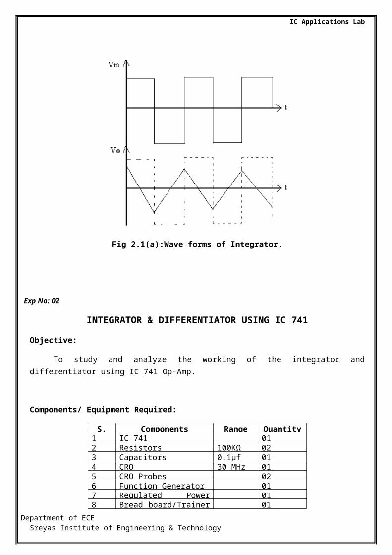
Fig 2.1(a):Wave forms of Integrator.
Department of ECE Sreyas Institute of Engineering & Technology
IC Applications Lab
Exp No: 02
INTEGRATOR & DIFFERENTIATOR USING IC 741
Objective:
To study and analyze the working of the integrator and differentiator using IC 741 Op-Amp.
Components/ Equipment Required:
S. No Components Range Quantity1 IC 741 012 Resistors 100KΩ 023 Capacitors 0.1µf 014 CRO 30 MHz 015 CRO Probes 026 Function Generator 017 Regulated Power Supply 018 Bread board/Trainer Kit 019 Connecting wires As required
Theory:
(PLEASE REFER CLASS NOTES / STANDARD TEXT BOOK
WHILE WRITING IN RECORD)
Integrator
A circuit in which the output voltage waveform is the integration of the input is called integrator.When we apply a square wave the frequency response is as shown in wave forms.
The above equation Indicates that the output voltage is directly proportional to the negative integral of the input voltage and inversely proportional to the time constant R f C1 . For Example if the input is a square wave, the output will be a triangular wave. or if the input is a sine wave output will be a cosine wave.
When Vin = 0 the integrator works as an open loop amplifier. This is because of the capacitor C1
acts as an open circuit (XC1 = infinite) to the input offset voltage Vin. In other words, the input offset voltage Vin and the part of the input current charging capacitor C1 produce the error voltage at the output of the integrator. To overcome this problem RF is connected across the feedback capacitor C1.Thus RF
limits the low-frequency gain and hence minimizes the variations in the output voltage.Frequency response (fb) of integrator at 0 dB is given by fb =1 / 2ΠR1C1.Both the stability and the low frequency roll-off problems can be corrected by the addition of resistors RF.The frequency response of practical integrator is as shown in the wave forms. In this ‘f’
Department of ECE Sreyas Institute of Engineering & Technology
IC Applications Lab
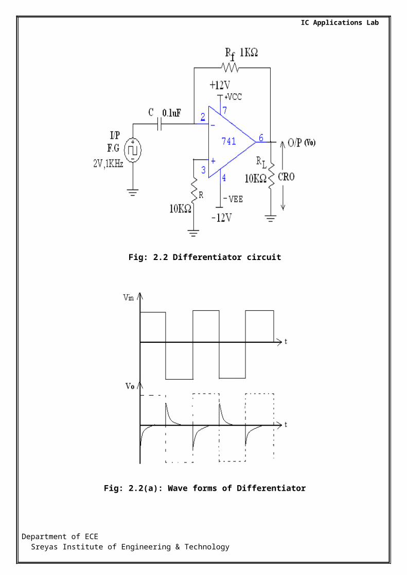
Fig: 2.2 Differentiator circuit
Fig: 2.2(a): Wave forms of Differentiator
Department of ECE Sreyas Institute of Engineering & Technology

IC Applications Lab
is relative operating frequency and for ‘f’ and f3 the gain RF/R1 is constant. However after fa the gain decreases at a rate of 20dB/decade. In other words, between fa and fb the circuit acts as an integrator. The gain-limiting frequency fa is given by fa =1/ 2πR C.The input signal will be integrated properly if the time period T of the input signal as larger than or equal to RF C1.
Differentiator:
The operational amplifier can e used in many applications. It can be used as differentiator and integrator. In differentiator the circuit performs the mathematical operation of differentiation that is the output waveform is the derivative of the input wave form for good differentiation, one must ensure that he time period of the input signal is larger than or equal to RfC1.the practical differentiator eliminates the problem of instability and high frequency noise.
The differentiator circuit performs the mathematical operation of differentiation. That is the output waveform is the derivative of the input waveform. Vo = - RF C1 (dVin / dt)
If a square wave is applied to the input of the differentiator then the output is spikes signal.If a sine wave is applied to the input of the differentiator then the output is cosine waveform.The reactance of the circuit (RF / XC1) increases with increase in frequency at a rate of 20dB per decade. This makes the circuit unstable.The input impedance XC1 decreases with increase in frequency, which makes the circuit very susceptible to high frequency noise.The frequency response of the basic differentiator is shown i In this figure is the frequency at which the gain is 0 dB.
Both the stability and the high – frequency noise problem can be corrected by the addition of two components R1 and C1 as shown in fig. The frequency response of which is shown in fig From f to fa the gain decreases at 20dB/decade. This 40 dB/decade change in gain is caused by the R1 C1 and RF C1
combinations. The gain limiting frequency fb is given by
R1 C1 and RF C1 help to reduce significantly the effect of high – frequency input, amplifier noise and offsets. Above all, it makes the circuit more stable by preventing the increase in gain with frequency. In general, the value of f1, and in turn R1 C1 and RF C1 should be selected such that fa=fb = fc unit gain – bandwidth.
The input signal will be differentiated properly if the time period T of the input signal is larger than or equal to RF C1.
Department of ECE Sreyas Institute of Engineering & Technology
IC Applications Lab
Observations:
!! MANDATORY:
ATTACH GRAPHS DRAWN ON GRAPH SHEETS HERE
Department of ECE Sreyas Institute of Engineering & Technology
IC Applications Lab
Procedure:
Integrator:
1. Connect the integrator circuit as shown in fig 2.1.2. Connect the 1MHz function generator to the input terminals and apply the input as square waveform.3. Connect the C.R.O at the output terminals.4. Switch ON fixed power supply,5. Observe and note down the output frequency and waveforms. (Sample output waveforms are as
shown in figures).6. Wave form shows the out response of square wave input.7. Repeat the above steps 1 to 5 to get the different waveforms, by varying the input frequency.8. Apply the sine wave, and repeat the above steps and observe the waveform.
Differentiator:
1. Connect the differentiator as shown in fig 2.2.2. Connect the function generator to the input terminals; apply sine wave at the input terminals.3. Connect the C.R.O at the output terminals.4. Switch ON the fixed power supply. 5. Observe and record the output frequency of waveforms (Ideal output waveforms are as shown in
fig)6. Repeat the above steps from 1 to 5 and observe different output waveforms, by varying the input
frequency.7. Apply the square wave, and repeat the above steps and observe the waveform. (Ideal waveforms)
are as shown in Fig.
Result:
The output waveforms of integrator and differentiator have been observed and plotted on the graph.
Review Questions:
1. Define differentiator.2. Define integrator3. What are the limitations of an ordinary differentiator?4. Explain how the practical differentiator will overcome the limitations5. What are the limitations of an ideal integrator?6. What are the initial conditions of a loss integrator?7. What are the differences between integrator and differentiator8. State the applications of integrator9. State the applications of differentiator10. Explain why integrators are preferred over differentiators in analog computer
Department of ECE Sreyas Institute of Engineering & Technology
IC Applications Lab
Circuit Diagrams:
Fig 3.1: High Pass Filter circuit
Fig 3.2: Low Pass Filter circuit
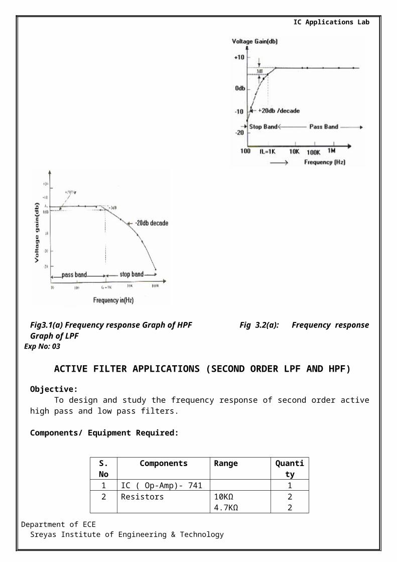
Fig3.1(a) Frequency response Graph of HPF Fig 3.2(a): Frequency response Graph of LPF
Department of ECE Sreyas Institute of Engineering & Technology

IC Applications Lab
Exp No: 03
ACTIVE FILTER APPLICATIONS (SECOND ORDER LPF AND HPF)
Objective: To design and study the frequency response of second order active high pass and low pass filters.
Components/ Equipment Required:
S. No Components Range Quantity
1 IC ( Op-Amp)- 741 12 Resistors 10KΩ
4.7KΩ22
3 Capacitors 0.01μf 24 CRO 30MHz 1
5 Function generator 0-1MHz 1
6 Bread board 1
7 Regulated Power Supply 1
8 CRO Probes 2
9 Connecting wires As required
Theory: (PLEASE REFER CLASS NOTES / STANDARD TEXT BOOK
WHILE WRITING IN RECORD)
High pass filter:
A device that passes high frequencies and attenuates (i.e., reduces the amplitude of) frequencies lower than the its cutoff frequency is called high pass filter. A high-pass filter is usually modeled as linear time-invariant system. It is sometimes called a low pass cutter or base-cut filter. High-pass filters have many uses, such as blocking DC from circuitry sensitive to non-zero average voltages or RF devices. They can also be used in conjunction with a low-pass filter to make a band pass filter. The actual amount of attenuation for each frequency is a design parameter of the filter.
Low-pass filter:
A filter that passes low-frequency signals but attenuates (reduces the amplitude of) signals with frequencies higher than the cutoff frequency called low pass filter. The actual amount of attenuation for each frequency varies from filter to filter. It is sometimes called a high-cut filter, or treble cut filter when used in audio applications. A low-pass filter is the opposite of a high-pass filter. A band-pass filter is a combination of a low-pass and a high-pass.
Low-pass filters exist in many different forms, including electronic circuits (such as a hiss filter used in audio), anti-aliasing filters for conditioning signals prior to analog-to-digital conversion, digital filters for smoothing sets of data, acoustic barriers, blurring of images, and so on. The moving average operation used in fields such as finance is a particular kind of low-pass filter, and can be analyzed with the same signal techniques as are used for other low-pass filters. Low-pass filters provide a smoother form of a signal, removing the short-term fluctuations, and leaving the longer-term trend.
Tabular form of HPF.Department of ECE Sreyas Institute of Engineering & Technology

IC Applications Lab
Vi=2V
Tabular form of LPF.Vi=2V
S. No Input Frequency ( Hz)
Output Voltage(Vo) in Volts
Gain =Vo / Vin
Gain in dB20 log (Vo /Vin)
Procedure:
Department of ECE Sreyas Institute of Engineering & Technology
S. No Input Frequency ( Hz)
Output Voltage(Vo) in Volts
Gain =Vo / Vin
Gain in dB20 log (Vo /Vin)
IC Applications Lab
High Pass Filter.
1. Connect circuit per the circuit diagram as shown in 3.1. 2. Connect the F.G at the input terminals and C.R.O at the output terminals.
3. Switch ON the power supply4. Give the sinusoidal signal of 2V p-p at the input.5. By varying the frequency of the input signal from 10 Hz to 1 MHz, note down the output
voltages and calculate gain in db.6. Plot the frequency response for HPF on Semilog Graph sheet.
Low Pass Filter.
1. Connect circuit per the circuit diagram as shown in 3.2.2. Connect the F.G at the input terminals and C.R.O at the output terminals.3. Switch ON the power supply4. Give the sinusoidal signal of 2V p-p at the input.5. By varying the frequency of the input signal from 10 Hz to 1 MHz, note down the output
voltages and calculate gain in db.6. Plot the frequency response for LPF on Semilog Graph sheet.
Result: The second order HPF & LPF is designed for chosen fL & fH and the frequency response curve is plotted between voltage gain (in dB) and frequency ( in Hz).
Review Questions:1. List the advantages of active filters over passive filter.2. Derive fH of second order LPF. & Derive fL of second order HPF.3. Draw the frequency response for ideal and practical filters of all types.4. What are the three design techniques used for design of filters.5. Compare butterworth and chebyshev filters.6. Design a first order low pass filter for 2 KHz frequency.7. Design a five pole low pass active butterworth filter with 3dB cut off frequency of 2 KHz.8. Show that the amplitude response of low pass butterworth filter well above cutoff decreases by
20dB per decade.
!! MANDATORY:
ATTACH GRAPHS DRAWN ON GRAPH SHEETS HERE
Circuit Diagram:
Department of ECE Sreyas Institute of Engineering & Technology
IC Applications Lab
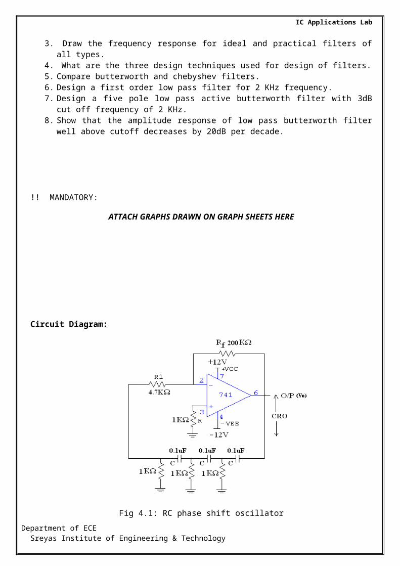
Fig 4.1: RC phase shift oscillator
Fig 4.1(a): Output of RC phase shift oscillator
Department of ECE Sreyas Institute of Engineering & Technology

IC Applications Lab
Exp No: 4
4. (a) RC PHASE SHIFT OSCILLATOR USING IC 741
Objective: To study the operation of RC phase shift oscillator and determination of the frequency of
oscillations.
Components/ Equipment Required:
S.No Components Range Quantity1 IC 741 012 Resistors 1KΩ
4.7KΩ200KΩ
040201
3 Capacitors 0.1uf 034 CRO 30 MHz 015 Regulated Power Supply 0-30V 1A 016 CRO Probes 027 Bread board/Trainer Kit 018 Connecting wires As required
Theory:(PLEASE REFER CLASS NOTES / STANDARD TEXT BOOK
WHILE WRITING IN RECORD)
The frequency of oscillations Fo is given by
At this frequency the gain Av must be at least be 29. That is
Thus the circuit will produce a sinusoidal waveform of frequency Fo if the gain is 29 and the total phase shift around the circuit is exactly 3600.
Procedure:
1. Connect the circuit diagram as shown above figure 4.1.2. From the given values of resistors (R) and capacitor (C), calculate theoretical frequency
(Fo =0.065/RC) and note down in the tabular column.3. Connect oscilloscope at output terminals and observe the output sine wave. 4. Adjust gain and shape of the sine wave by using potentiometer Rf.5. Compare the theoretical and practical frequencies.
Result: Operation of RC-Phase shift oscillator using IC 741 is studied and frequency of oscillations is determined.
Department of ECE Sreyas Institute of Engineering & Technology
IC Applications Lab
Circuit Diagram:
Fig 4.2: Wein – Bridge Oscillator
Fig 4.2(a): Output of Wein – Bridge Oscillator
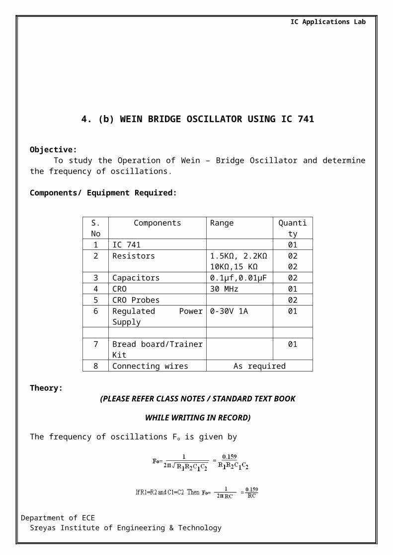
4. (b) WEIN BRIDGE OSCILLATOR USING IC 741
Department of ECE Sreyas Institute of Engineering & Technology

IC Applications Lab
Objective: To study the Operation of Wein – Bridge Oscillator and determine the frequency of oscillations.
Components/ Equipment Required:
S. No Components Range Quantity1 IC 741 012 Resistors 1.5KΩ, 2.2KΩ
10KΩ,15 KΩ0202
3 Capacitors 0.1µf,0.01µF 024 CRO 30 MHz 015 CRO Probes 026 Regulated Power Supply 0-30V 1A 01
7 Bread board/Trainer Kit 018 Connecting wires As required
Theory:(PLEASE REFER CLASS NOTES / STANDARD TEXT BOOK
WHILE WRITING IN RECORD)
The frequency of oscillations Fo is given by
At this frequency the gain Av must be at least be 3. That is
Thus the circuit will produce a sinusoidal waveform of frequency Fo if the gain is 3 and the total phase shift around the circuit is exactly 3600.
Procedure:1. Connect the circuit as shown in the figure 4.2 .2. Connect the C.R.O at the output terminals and observe the output waveform.3. Observe and record the output waveforms by varying the resistance of potentiometer.4. a) Calculate the value of frequency when the POT is in minimum position.
b) Similarly, calculate the frequency f for POT at maximum position.5. Compare the theoretical and practical values.
Result: Operation of Wein –Bridge Oscillator experiment is studied and frequency of oscillations is determined.
Observations:
Department of ECE Sreyas Institute of Engineering & Technology

IC Applications Lab
!! MANDATORY:
ATTACH GRAPHS DRAWN ON GRAPH SHEETS HERE
Review Questions:Department of ECE Sreyas Institute of Engineering & Technology
IC Applications Lab
1. What is the phase shift provided by each RC section at the frequency of oscillation?2. On what factors does the oscillator frequency depend on?3. What ranges of frequencies are obtained by this oscillator?4. What are Barkhusen’s criteria for oscillations?5. What type of feedback does the phase shift RC network provide?6. What is the function of Rf in the oscillator circuit?7. Derive Fo of phase shift oscillator.8. Compare RC oscillators with crystal oscillator.9. What change do you find by changing different R-C networks in the circuit?10. How do you vary the gain of the oscillator?11. State Barkhausen’s criterion for oscillations.12. Derive the frequency of oscillations and gain of wein bridge oscillator.13. List out different types of oscillators.14. What is the function of Pot R3 in the wein bridge oscillator circuit?15. What is the advantage by using IC 741 op-amp in the oscillator circuit?16. Why RC oscillators are called low frequency oscillators.17. What is the frequency range you can get from the oscillator circuit?18. How do you vary the gain of the oscillator?
Circuit Diagram:
Department of ECE Sreyas Institute of Engineering & Technology
IC Applications Lab
Fig 5.1: IC 555 timer as a Monostable Multivibrator
Pulse width=TP = 1.1 RC.
Fig 5.2 Monostable Multivibrator Output
Exp No: 5
Department of ECE Sreyas Institute of Engineering & Technology

IC Applications Lab
MONOSTABLE MULTIVIBRATOR USING IC 555
Objectives:
1.To design and observe the output waveforms IC 555 timer as a Monostable Multivibrator.
2. To Calculate pulse width and the frequency of oscillations of Monostable Multivibrator.
Components/ Equipment Required:
S. No Components Range No
1 IC 555 ---- 012 Resistors 10KΩ 02
3 Capacitors 0.01µf0.1µf
0201
4 CRO 30 MHz 01
5 Regulated Power Supply 0-30V 1A
01
6 CRO probes 027 Bread board or trainer kit 01
8 Connecting wires As required
Theory:
(PLEASE REFER CLASS NOTES / STANDARD TEXT BOOK
WHILE WRITING IN RECORD)
Monostable can also called as One-shot Multivibarator, below fig Shows the Monostable
Multivibrator. When the output is low, the circuit is in stable state, Transistor Q1 is ON and capacitor C
is shorted out to ground. However, upon application of a negative trigger pulse to pin-2, transistor Q1 is
turned OFF, which releases short circuit across the external capacitor and drives the output High. The
capacitor C now starts charging up toward Vcc through R2. However, when the voltage across the
external capacitor equals 2/3 Vcc, comparator-1 output switches from low to high, which is turn drives
the output to its low state via the output of the flip flop turns transistor Q1 ON, and hence, capacitor C
rapidly discharges through the transistor. The output of the Monostable remains low until a trigger pulse
is again applied. Then the cycle repeats. Fig 5.2 shows the trigger input and output voltages, and
capacitor voltage waveforms. Pulse width of the trigger input must be smaller than the expected pulse
width of the output waveforms. Trigger pulse must be a negative going input signal with amplitude larger
than 1/3 Vcc. The time during which the output remains high is given by Tp =1.1R2C, Once triggered, the
circuit’s output will remain in the high state until the set time Tp elapses. The output will not change its
state even if an input trigger is applied again during this time interval Tp.
Observations:
Department of ECE Sreyas Institute of Engineering & Technology

IC Applications Lab
!! MANDATORY:
ATTACH GRAPHS DRAWN ON GRAPH SHEETS HERE
Procedure:Department of ECE Sreyas Institute of Engineering & Technology

IC Applications Lab
1. Connect the circuit of 555 timer as monostable mode as shown in fig 5.1.2. Connect the C.R.O at the output terminals.3. Apply external negative going trigger at the input terminal (pin-2).4. Record and observe the waveforms at the output terminals and also across the capacitor.5. Verify with the sample output waveforms as per expected wave forms.6. Plot the output waveforms with respect to input trigger.7. Calculate the pulse width, time period of pulse (Tp) theoretically and verify with practical
values.8. Now change R2 value and observe out pulse width Tp and verify it theoretically.
Tp = 1.1 R2 C.
Result: The output waveforms of monostable multivibrator are observed and plotted and pulse width is calculated.
Review Questions:1.List the important features of the 555 Timer.2. Define Duty cycle.3. What are the modes of operation of Timer and explain the differences between two
operating modes of the 555 Timer.4. The Monostable monostable circuit is to be used as a divided by 2 network. The
frequency of the input trigger signal is 2 KHz. If the value of C=0.01 μF, what should be the value of RA (Let tp =1.2T).
5. Consider the Monostable monostable with R=3KΩ and C=0.0068μF.Determine the pulse width.
6. Design a Monostable monostable to produce an output pulse 2 m sec wide.7. What is the function of control input (pin5) of 555 timers?8. List the applications of 555 timers in monostable mode.9. Why do we use negative trigger for monostable operation?10. Explain the trigger circuit used for monostable multivibrator.
Circuit Diagram:
Department of ECE Sreyas Institute of Engineering & Technology
IC Applications Lab
Fig: 6.1(a): Schmitt trigger circuit using IC 741
Fig: 6.1(b): Output waveform of Schmitt Trigger
Exp No: 6
Department of ECE Sreyas Institute of Engineering & Technology
IC Applications Lab
6(a) SCHMITT TRIGGER USING IC 741
Objective:
To design and study the Schmitt trigger circuit using IC 741 op-amp.
Components/ Equipment Required:
S. No Components Range No
1 IC 741 ---- 012 Resistors 10KΩ 043 CRO 30 MHz 014 Function generator 1MHz 015 Regulated Power Supply 0-30V 1A 016 CRO probes 027 Bread board or trainer kit 018 Connecting wires As required
Theory:
(PLEASE REFER CLASS NOTES / STANDARD TEXT BOOK WHILE WRITING IN RECORD)
This circuit converts a sine waveform into a square waveform or pulse. The circuit is known as Schmitt trigger or squaring circuit. The input voltage Vin trigger (changes state of) the output Vo every time it exceeds certain levels called the upper threshold voltage VUT and lower threshold voltage VLT.
These threshold voltages are obtained by using the voltage divider R1 R2 where the voltage across R1 is feedback to (+) input. The voltage across R1 is a variable reference threshold voltage that depends on the value and polarity of the output voltage Vo. When Vo = +Vsat , the voltage across R1 is called the upper threshold voltage, VUT. The input voltage Vin must be slightly more positive than VUT in order to cause the output vo to swing from +vsat to –Vsat. As long as Vin< Vut, Vo is at +Vsat. Using the voltage divider rule,
Vut is given by the following equation,VUT = (R2/R1+R2)(+V sat)
On the other hand, when V o= -V sat, the voltage across R1 is referred as lower threshold voltage, V lt. V in must be slightly more negative than V LT in order to cause Vo switch from –V sat to +V sat. In their words, for V in values greater than VLT, V o is at –V sat.
Vlt is given by the following equation,VLT= (R1/R1+R2) (-Vsat)Thus if the threshold voltages are made larger than the noise voltages, the positive feedback will
eliminate the false output transitions. Also, the positive feedback, because of its regeneration action, will make Vo switch faster between +V sat and –V sat.
In general non inverting comparator is used as a Schmitt trigger. If the input is triangular wave or saw tooth wave, the output will be square wave or pulse wave respectively. The comparator with positive feedback is said to exhibit hysteresis, a dead band condition. That is, when input of the comparator exceeds Vut, its output switches from +Vsat to –Vsat and reverse back to its original state, +Vsat, when input goes below Vlt.
Therefore Vhy= VUT - VLT = (R1/R1+R2) [+Vsat - (-Vsat)]
Observations:
Department of ECE Sreyas Institute of Engineering & Technology
IC Applications Lab
!! MANDATORY:
ATTACH GRAPHS DRAWN ON GRAPH SHEETS HERE
Procedure:
Department of ECE Sreyas Institute of Engineering & Technology
IC Applications Lab
1. Connect the circuit diagram as shown in the figure 6.1(a).2. Give the input 5V (p-p) of 1 KHz frequency sine wave from the function generator.3. Observe the output at 3rd pin of the IC 741.4. Observe and compare the input and out put waveform and indicate UTP & LTP and calculate VH
= VUT - VLT.
5. Plot the input and output waveforms.
Result: The input and output waveforms of Schmitt trigger using IC 741 are observed and UTP & LTP are located.
Circuit Diagram:
Department of ECE Sreyas Institute of Engineering & Technology

IC Applications Lab
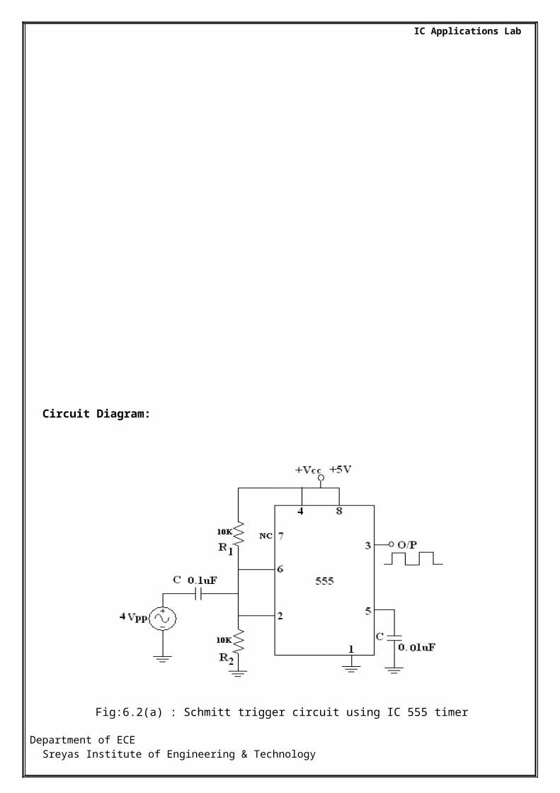
Fig:6.2(a) : Schmitt trigger circuit using IC 555 timer
Fig:6.2(b) : Output Waveforms of Schmitte trigger
6(b) SCHMITT TRIGGER USING IC 555
Department of ECE Sreyas Institute of Engineering & Technology
IC Applications Lab
Objective:
To design and study the Schmitt trigger circuit using IC 555 timer.
Components/ Equipment Required:
S. No Name of the Apparatus Range No1 IC 555 ---- 012 Resistors 10KΩ 023 Capacitors 0.01µf
0.1µf0101
4 CRO 30 MHz 015 Function generator 1MHz 016 Regulated Power Supply 0-30V 1A 017 CRO probes 028 Bread board or trainer kit 019 Connecting wires As required
Theory:
(PLEASE REFER CLASS NOTES / STANDARD TEXT BOOK WHILE WRITING IN RECORD)
The circuit shown is an inverting comparator with positive feed back. This circuit converts an irregular shaped wave form to a square wave or pulse. The circuit is known as Schmitt trigger or squaring circuit. The input voltage triggers the output every time it exceeds certain voltage levels called upper threshold voltage and lower threshold voltage.
If the threshold voltages VUT &VLT are made larger than the input noise voltages, the positive feedback will eliminate the pulse transitions.
Fig 1.3 shows that the output of the Schmitt trigger is a square wave when the input is a sine wave. A slightly different version of the Schmitt trigger is used in the triangular wave and saw-tooth wave generators. In this generators a non- inverting comparators is used as a Schmitt trigger
When the input is a sine wave the output of the Schmitt trigger is a square wave and if the input is sawtooth wave the output is a pulse waveform.
Procedure:
1. Connect the circuit diagram as shown in the figure.2. Give the input 5V (p-p) of 1 KHz frequency sine wave from the function generator.3. Observe the output at 3rd pin of the IC555.4. Observe and compare the input and out put waveform and indicate UTP & LTP and calculate VH
= VUT - VLT.
5. Plot the input and output waveforms.
Observations:
Department of ECE Sreyas Institute of Engineering & Technology
IC Applications Lab
!! MANDATORY:
ATTACH GRAPHS DRAWN ON GRAPH SHEETS HERE
Department of ECE Sreyas Institute of Engineering & Technology
IC Applications Lab
Result: The input and output waveforms of Schmitt trigger using IC 555 are observed and UTP &
LTP are located.
Review Questions:
1. Explain how a square wave is obtained at the output of IC 555 timer when sine wave input is given.
2. What type of waveform is obtained when triangular or ramp waveforms are applied to Schmitt trigger circuit?
3. Explain how upper trigger and lower trigger levels are obtained in the Schmitt trigger circuit.4. Why do we short pin 2 and pin 6 of IC 555 timer for Schmitt trigger operation.5. Why do we connect pin 4 of 555 timers to Vcc.6. What is the function of pull up resistor RL in the Schmitt trigger circuit?7. Why do we call Schmitt trigger as square wave generator.8. How do you vary the duty cycle of the output waveform?
Circuit Diagram:
Department of ECE Sreyas Institute of Engineering & Technology

IC Applications Lab
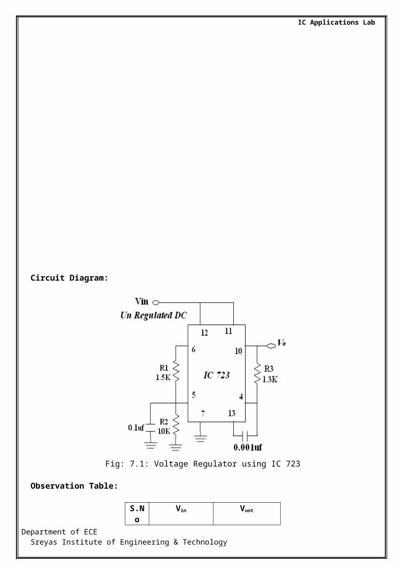
Fig: 7.1: Voltage Regulator using IC 723
Observation Table:
S.No
Vin Vuot
Exp No: 07
Department of ECE Sreyas Institute of Engineering & Technology
IC Applications Lab
VOLTAGE REGULATOR USING IC 723
Objective: To design a low voltage Regulator using IC 723.
Components/ Equipment Required:
Theory: (PLEASE REFER CLASS NOTES / STANDARD TEXT BOOK
WHILE WRITING IN RECORD)
The IC 723 is a monolithic integrated circuit voltage regulator featuring high ripple rejection, excellent input and load regulation, excellent temperature stability etc.,
It consists of a temperature compensating reference voltage amplifier, an error amplifier, 150mA output transistor and an adjustable output current limiter.
The basic low voltage regulator type IC723 circuit is shown in figure .The unregulated input voltage is 24V and the regulated output voltage is from 0.2V to 7.3V by varying POT R. R SC (R1) is connected across current sense (Cs) and current limit (CL) terminals to limit the accidental short circuit current.
A stabilizing capacitor (C1) of 100pF is connected between frequency compensation terminal and inverting (INV) terminal. External NPN pass transistor is added to the basic IC 723-regulator circuit to increase its load current capability.
The output voltage can be regulated from 7 to 37Volts for an input voltage range from 9.5Volts to 40Volts. For intermediate output voltages the following formula can be used.
The resistor values R1 and R2 are calculated from potential divider network.
Observations:
Department of ECE Sreyas Institute of Engineering & Technology
S.no Components Range Qty
1 IC 723 - 1
2 Capacitors 0.1uf ,0.001uf 2
3 Resistors 1.3k,1.5k,10k 3
4 CRO 20 MHz 1
5 Function generator 1Hz-1MHz 1
6 Regulated Power Supply 0-30V 1A 1
7 Power supply 0-30V 1
8 Bread Board 1
9 Connecting wires As required

IC Applications Lab
!! MANDATORY:
ATTACH GRAPHS DRAWN ON GRAPH SHEETS HERE
Department of ECE Sreyas Institute of Engineering & Technology
IC Applications Lab
Design Procedure:
Vref = 7.15 (typical value) . Vo is given by, Vo =Vref x R2 / R1 =R2
Assume any value for R1 or R2 solve it, R3 is given by, R3= R1// R2
Procedure:
1. Give the connections as per the circuit diagram as shown in fig 7.1.2. By varying input DC voltage from 9.5V to 40V, observe the output voltage.3. Note done the readings of input DC voltage and output voltage in the tabular form.
Result: Thus the voltage regulator is constructed using IC723 and its regulation characteristics are tested.
Review Questions:
1. What is the function of a voltage regulator?2. What is a voltage reference? Why is it needed?3. Draw the functional block diagram of IC 723 regulators and explain?4. Design a high voltage and low voltage regulator using IC 723.5. Define line and load regulation of a regulator?6. List the features of a voltage regulator IC 723.7. List the different types of IC voltage regulators8. What is the output voltage range of an IC 723 voltage regulator?9. What is the function of CL & CS terminals of IC 723 regulator?10. What is the difference between a series and shunt voltage regulator?11. What is the difference between a linear and switching regulator.12. What are the basic units / elements of a voltage regulator?
Department of ECE Sreyas Institute of Engineering & Technology
IC Applications Lab
Fig: 8.1: Pin Configuration of 74189
Table: 8.1
S.NoAddress
A3 A2 A1 A0
DataD4 D3 D2 D1
Complement of DataD4 D3 D2 D1
1
2
3
4
Exp No: 08
Department of ECE Sreyas Institute of Engineering & Technology
IC Applications Lab
4-BIT RAM USING IC 74189 READ & WRITE OPERATIONS
Objective: To implement RAM using IC 74189 ; write & read 4-bit data in it.
Equipment Required: 1. 4-Bit RAM Using IC 74189 Trainer kit.2. Connecting Wires
Theory:The 74LS189 is a high speed 64-bit Ram organized as a 16- word by 4-bit array. Address inputs
are buffered to minimize loading and are fully decoded on-chip. The outputs are 3-state and are in the high impedance state whenever the Memory Enable (ME) input is HIGH. The outputs are active only in the Read mode and the output data is the complement of the stored data. Here A0-A3 are the Address Inputs, D1-D4 are Data inputs, DO1-DO4are Inverted Data Outputs
Procedure:1. Study the Pin diagram of IC 74189.2. Connect Logic inputs to the pins meant for address bits i.e A0,A1,A2 & A3.3. Connect the Logic inputs for pins meant for Data bits i.e D1,D2,D3& D4
4. Connect CE(Chip Enable) to logic input.
5. Connect R/ to logic input.6. Connect output pins D01, D02, D03 & D04 to output indicator LEDs.
Write Operation:7. Initially keep all logic inputs in 0 state.8. Select required data to be stored in RAM using logic inputs.9. Select required address location where the data should be stored using logic inputs.10. Enable chip by changing CE to high from low( bring it to low again after 2 seconds).11. Now the data will be stored in IC in complement form to original.
Read Operation:
12. Change R/ to logic 1(Now the IC is in Read mode).13. Select the address from which we want data to be retrieved.13. Observe the output at LEDs, which is complement of input data applied.
Result:
Viva Questions:1. What is the RAM?2. Give the applications of the RAM?3. What is the difference between RAM &ROM?4. What is the difference between static RAM &dynamic RAM?5. Which can be used as 1-bit memory?6. What are the different types of the ROM?7. What are the parameters of the RAM?8. What is refreshing of memory? And where it is required?9. What are sequential access memories?10. What are charge-coupled devices?
Department of ECE Sreyas Institute of Engineering & Technology
IC Applications Lab
Fig: 9.1: Pin Configuration of 74189
Table: 9.1
S.NoAddress
A3 A2 A1 A0
DataD4 D3 D2 D1
Complement of DataD4 D3 D2 D1
1 0 0 0 0
2 0 0 0 1
3 0 0 1 0
4 0 0 1 1
5 0 1 0 0
6 0 1 0 1
7 0 1 1 0
8 0 1 1 1
9 1 0 0 0
10 1 0 0 1
11 1 0 1 0
12 1 0 1 1
13 1 1 0 0
14 1 1 0 1
15 1 1 1 0
16 1 1 1 1
Exp No: 09
Department of ECE Sreyas Institute of Engineering & Technology

IC Applications Lab
STACK & QUEUE IMPLEMENTATION USING IC 74189
Objective: To implement Stack & Queue using IC 74189.
Equipment Required: 1. 4-Bit RAM Using IC 74189 Trainer kit.2. Connecting Wires
Theory:The 74LS189 is a high speed 64-bit Ram organized as a 16- word by 4-bit array. Address inputs
are buffered to minimize loading and are fully decoded on-chip. The outputs are 3-state and are in the high impedance state whenever the Memory Enable (ME) input is HIGH. The outputs are active only in the Read mode and the output data is the complement of the stored data. Here A0-A3 are the Address Inputs, D1-D4 are Data inputs, DO1-DO4are Inverted Data Outputs
Procedure:1. Study the Pin diagram of IC 74189.2. Connect Logic inputs to the pins meant for address bits i.e A0,A1,A2 & A3.3. Connect the Logic inputs for pins meant for Data bits i.e D1,D2,D3& D4
4. Connect CE(Chip Enable) to logic input.
5. Connect R/ to logic input.6. Connect output pins D01, D02, D03 & D04 to output indicator LEDs.7. Initially keep all logic inputs in 0 state.8. Select required data to be stored in RAM using logic inputs.9. Select required address location where the data should be stored using logic inputs.10. Enable chip by changing CE to high from low( bring it to low again after 2 seconds).11. Now the data will be stored in IC in complement form to original.12. Repeat steps 8 to 10 for all possible address combinations.Stack Implementation:
13. Change R/ to logic 1(Now the IC is in Read mode).14. Read all the data stored in IC in LIFO( Last in First Out) order.Queue Implementation:15. Read all the data stored in IC in FIFO( First in First Out) order.16. Verify the values stored in IC in their correspond addresses.
Result:
Department of ECE Sreyas Institute of Engineering & Technology
IC Applications Lab
Figure 10.1. (a) A simple S/H circuit. (b) A practical S/H circuit.
Figure 10.2 (a) Original signal. (b) Sample and hold cycles. (c) Capacitor droop.
Figure 10.3 LF398 block diagram and S/H experiment circuit connections.
Department of ECE Sreyas Institute of Engineering & Technology
IC Applications Lab
Exp No: 10
SAMPLE & HOLD CIRCUIT USING LF398
Objective: To implement and analyze sample and hold circuit using LF 398
Equipment Required: 1. Sample & Hold Circuit Trainer kit.2. Function Generator 1 No3. CRO 1No4. Connecting Wires
Theory:A/D circuits require the input signal to remain constant during the conversion process; however,
real world signals may fluctuate rapidly. The Sample and Hold (S/H) is a device that makes its output follow the input until it is told to hold this value. It then maintains the output as steady as possible, regardless of fluctuations of the input, until released to follow the input again. This assures that the A/D is not trying to hit a moving target.
In its simplest form, the S/H circuit consists of a switch (S) and a capacitor (C) as in figure 10.1(a). When the switch S is closed, the capacitor C is charged to the value of the input voltage, the sample stage. Afterwards the switch is opened and the capacitor retains its charge, the hold stage. The resulting output is shown in figure 10.2-b. This alternation between sample and hold modes is repeated as long as the switch keeps toggling. The switching rate is controlled by a clock signal whose frequency should satisfy the Nyquist sampling criterion. A practical implementation of the S/H circuit is shown in figure 10.1(b). The switch is a FET whose gate is controlled by the clock pulse. Buffers are placed at the input and output to isolate the circuit.
The LF398 S/H Integrated Circuit The LF398 is a basic and common S/H monolithic IC, figure 10.3. It consists of an input and
output buffer amplifiers, and a digital switch. The hold capacitor is connected externally. During the sample mode, the capacitor is connected to the output of the input amplifier A, and during the hold mode, to the input of the output amplifier B. Amplifier B is a unity gain follower, of FET type for high input and low output resistances. Amplifier A is bipolar with low output offset voltage and wide bandwidth. The external capacitor is charged from a current source through the logic controlled switch. Amplifier C is a digital switch, which is turned on when the logic input drops below the reference voltage. The output of amplifier B is fed back to amplifier A.
During the sample mode, the charge on the capacitor follows the analog input signal. In the hold mode, the input amplifier is disconnected and the capacitor holds the charge. The capacitor is discharged by the follower amplifier.
Procedure:
Result:
Department of ECE Sreyas Institute of Engineering & Technology
IC Applications Lab
APPENDIX-1
Some Other Circuits to implement above experiments
Monostable circuit using 555
Department of ECE Sreyas Institute of Engineering & Technology
IC Applications Lab
Department of ECE Sreyas Institute of Engineering & Technology
![NP-Complete Problems Algorithm : Design & Analysis [23]](https://static.fdocuments.net/doc/165x107/5697bfcf1a28abf838ca9de4/np-complete-problems-algorithm-design-analysis-23.jpg)


