Complementary silicon power transistors - … · COMPLEMENTARY SILICON POWER TRANSISTORS ......
6
BD909/911 BD910/912 COMPLEMENTARY SILICON POWER TRANSISTORS ■ STMicroelectronics PREFERRED SALESTYPES DESCRIPTION The BD909 and BD911 are silicon Epitaxial-Base NPN power transistors mounted in Jedec TO-220 plastic package. They are intented for use in power linear and switching applications. The complementary PNP types are BD910 and BD912 respectively. INTERNAL SCHEMATIC DIAGRAM October 1999 ABSOLUTE MAXIMUM RATINGS Symbol Parameter Value Unit NPN BD909 BD911 PNP BD910 BD912 V CBO Collector-Base Voltage (I E = 0) 80 100 V VCEO Collector-Emitter Voltage (I B = 0) 80 100 V V EBO Emitter-Base Voltage (I C = 0) 5 V I E ,I C Collector Current 15 A I B Base Current 5 A Ptot Total Dissipation at T c ≤ 25 o C 90 W T stg Storage Temperature -65 to 150 o C Tj Max. Operating Junction Temperature 150 o C For PNP types voltage and current values are negative. 1 2 3 TO-220 ® 1/6
Transcript of Complementary silicon power transistors - … · COMPLEMENTARY SILICON POWER TRANSISTORS ......
BD909/911BD910/912
COMPLEMENTARY SILICON POWER TRANSISTORS
■ STMicroelectronics PREFERREDSALESTYPES
DESCRIPTION The BD909 and BD911 are silicon Epitaxial-BaseNPN power transistors mounted in Jedec TO-220plastic package. They are intented for use inpower linear and switching applications.The complementary PNP types are BD910 andBD912 respectively.
INTERNAL SCHEMATIC DIAGRAM
October 1999
ABSOLUTE MAXIMUM RATINGS
Symbol Parameter Value Unit
NPN BD909 BD911
PNP BD910 BD912
VCBO Collector-Base Voltage (IE = 0) 80 100 V
VCEO Collector-Emitter Voltage (IB = 0) 80 100 V
VEBO Emitter-Base Voltage (IC = 0) 5 V
IE,IC Collector Current 15 A
IB Base Current 5 A
Ptot Total Dissipation at Tc ≤ 25 oC 90 W
Tstg Storage Temperature -65 to 150 oC
Tj Max. Operating Junction Temperature 150 oC For PNP types voltage and current values are negative.
12
3
TO-220
®
1/6
THERMAL DATA
Rthj-case Thermal Resistance Junction-case Max 1.4 oC/W
ELECTRICAL CHARACTERISTICS (Tcase = 25 oC unless otherwise specified)
Symbol Parameter Test Conditions Min. Typ. Max. Unit
ICBO Collector Cut-offCurrent (IE = 0)
for BD909/910 VCB = 80 Vfor BD911/912 VCB = 100 VTcase = 150 oCfor BD909/910 VCB = 80 Vfor BD911/912 VCB = 100 V
500500
55
µAµA
mAmA
ICEO Collector Cut-offCurrent (IB = 0)
for BD909/910 VCE = 40 Vfor BD911/912 VCE = 50 V
11
mAmA
IEBO Emitter Cut-off Current(IC = 0)
VEB = 5 V 1 mA
VCEO(sus)∗ Collector-EmitterSustaining Voltage (IB = 0)
IC = 100 mA for BD909/910 for BD911/912
80100
VV
VCE(sat)∗ Collector-EmitterSaturation Voltage
IC = 5 A IB = 0.5 AIC = 10 A IB = 2.5 A
13
VV
VBE(sat)∗ Base-EmitterSaturation Voltage
IC = 10 A IB = 2.5 A 2.5 V
VBE∗ Base-Emitter Voltage IC = 5 A VCE = 4 V 1.5 V
hFE∗ DC Current Gain IC = 0.5 A VCE = 4 VIC = 5 A VCE = 4 VIC = 10 A VCE = 4 V
40155
250150
fT Transition frequency IC = 0.5 A VCE = 4 V 3 MHz∗ Pulsed: Pulse duration = 300 µs, duty cycle 1.5 %For PNP types voltage and current values are negative.
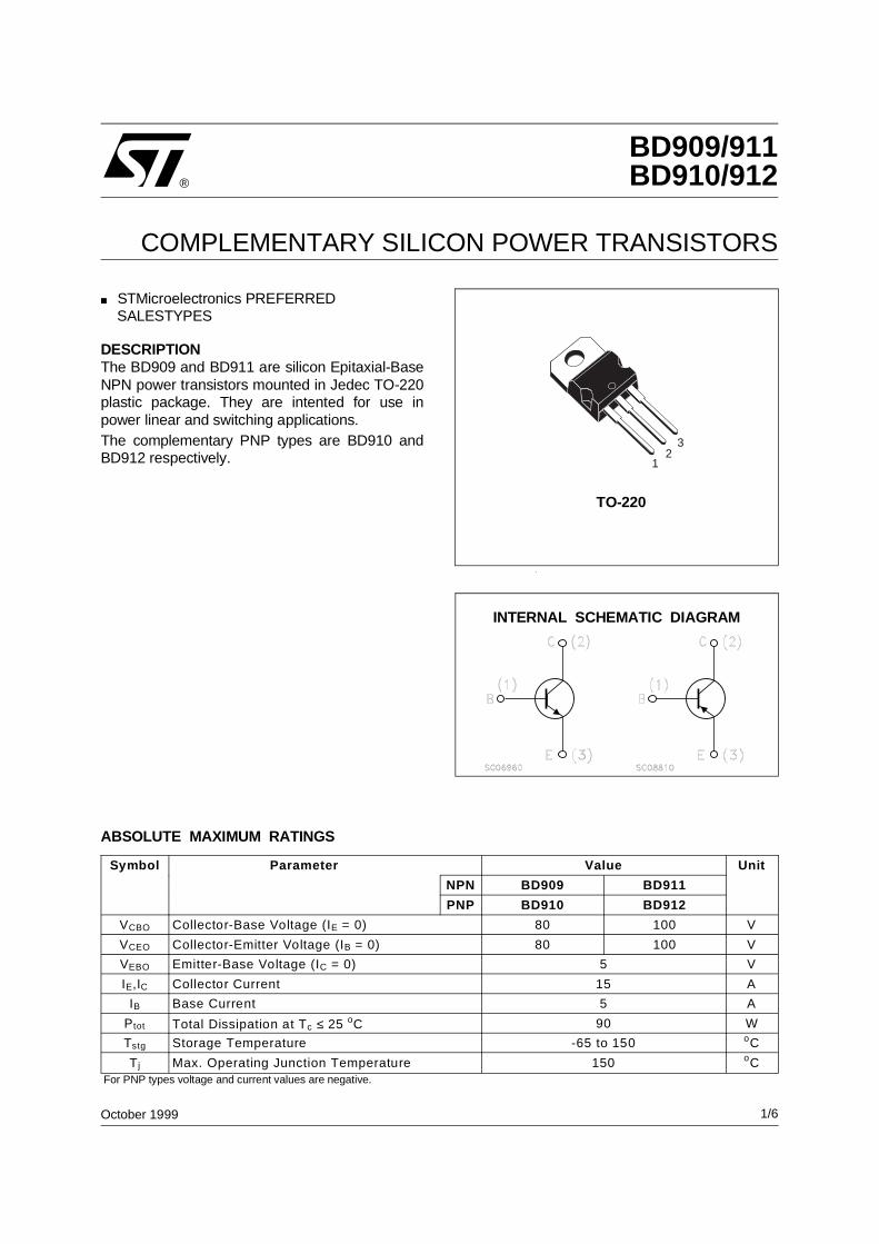
Safe Operating Area Derating Curves
BD909 / BD910 / BD911 / BD912
2/6
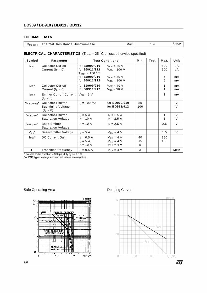
DC Current Gain (NPN type)
DC Transconductance (NPN type)
Collector-Emitter Saturation Voltage (NPN type)
DC Current Gain (PNP type)
DC Transconductance (PNP type)
Collector-Emitter Saturation Voltage (PNP type)
BD909 / BD910 / BD911 / BD912
3/6
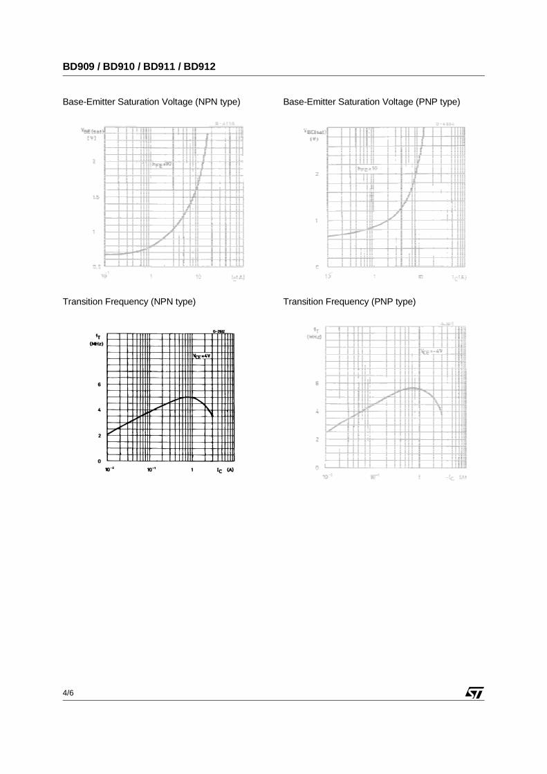
Base-Emitter Saturation Voltage (NPN type)
Transition Frequency (NPN type)
Base-Emitter Saturation Voltage (PNP type)
Transition Frequency (PNP type)
BD909 / BD910 / BD911 / BD912
4/6

DIM.mm inch
MIN. TYP. MAX. MIN. TYP. MAX.
A 4.40 4.60 0.173 0.181
C 1.23 1.32 0.048 0.051
D 2.40 2.72 0.094 0.107
D1 1.27 0.050
E 0.49 0.70 0.019 0.027
F 0.61 0.88 0.024 0.034
F1 1.14 1.70 0.044 0.067
F2 1.14 1.70 0.044 0.067
G 4.95 5.15 0.194 0.203
G1 2.4 2.7 0.094 0.106
H2 10.0 10.40 0.393 0.409
L2 16.4 0.645
L4 13.0 14.0 0.511 0.551
L5 2.65 2.95 0.104 0.116
L6 15.25 15.75 0.600 0.620
L7 6.2 6.6 0.244 0.260
L9 3.5 3.93 0.137 0.154
DIA. 3.75 3.85 0.147 0.151
P011C
TO-220 MECHANICAL DATA
BD909 / BD910 / BD911 / BD912
5/6
Information furnished is believed to be accurate and reliable. However, STMicroelectronics assumes no responsibility for the consequencesof use of such information nor for any infringement of patents or other rights of third parties which may result from its use. No license isgranted by implication or otherwise under any patent or patent rights of STMicroelectronics. Specification mentioned in this publication aresubject to change without notice. This publication supersedes and replaces all information previously supplied. STMicroelectronics productsare not authorized for use as critical components in life support devices or systems without express written approval of STMicroelectronics.
The ST logo is a trademark of STMicroelectronics
© 1999 STMicroelectronics – Printed in Italy – All Rights ReservedSTMicroelectronics GROUP OF COMPANIES
Australia - Brazil - China - Finland - France - Germany - Hong Kong - India - Italy - Japan - Malaysia - Malta - Morocco - Singapore - Spain - Sweden - Switzerland - United Kingdom - U.S.A.
http://www.st.com.
BD909 / BD910 / BD911 / BD912
6/6