Complementary high-speed SiGe and CMOS buffers - InTech
24
Complementary high-speed SiGe and CMOS buffers 227 0 Complementary high-speed SiGe and CMOS buffers Esa Tiiliharju University of Turku Finland 1. Introduction This chapter on high speed buffers in complementary SiGe and CMOS technologies studies three different buffer application areas, that is PA-driving, balun buffers, and finally LNAs. The underlaying idea of this text is to point out the benefits obtainable from the application of complementary analog signal processing techniques. More specifically, the text will study applications of the inverter-like continuously biased current-reuse stage in different buffering purposes. One implementation example is shown in the attached Fig. 1, where a continuously current-biased gain cell uses the complementary PMOS to generate extra transconductance. A challenge for microwave applications of this current-reuse cell is to find ways to deal with the added parasitic capacitance associated with the complementary device. Vdd in out bias Fig. 1. A CMOS current-reuse cell. First the reader will be introduced to the subject through a review on complementary bipolar devices in Section 2, including a discussion on a 10-GHz SiGe version of the “compound” emitter-follower. Integrated buffers with balun functionality will follow next in Section 3, 12 www.intechopen.com
Transcript of Complementary high-speed SiGe and CMOS buffers - InTech
Complementary high-speed SiGe and CMOS buffers 227
Complementary high-speed SiGe and CMOS buffers
Esa Tiiliharju
0
Complementary high-speed
SiGe and CMOS buffers
Esa TiiliharjuUniversity of Turku
Finland
1. Introduction
This chapter on high speed buffers in complementary SiGe and CMOS technologies studiesthree different buffer application areas, that is PA-driving, balun buffers, and finally LNAs.The underlaying idea of this text is to point out the benefits obtainable from the applicationof complementary analog signal processing techniques. More specifically, the text will studyapplications of the inverter-like continuously biased current-reuse stage in different bufferingpurposes. One implementation example is shown in the attached Fig. 1, where a continuouslycurrent-biased gain cell uses the complementary PMOS to generate extra transconductance.A challenge for microwave applications of this current-reuse cell is to find ways to deal withthe added parasitic capacitance associated with the complementary device.
Vdd
inout
bias
Fig. 1. A CMOS current-reuse cell.
First the reader will be introduced to the subject through a review on complementary bipolardevices in Section 2, including a discussion on a 10-GHz SiGe version of the “compound”emitter-follower. Integrated buffers with balun functionality will follow next in Section 3,
12
www.intechopen.com

Advanced Microwave Circuits and Systems228
where the reader focus is directed towards FET technologies. Albeit most of the baluns pre-sented in this section have originally been implemented in GaAs, they are realizable in CMOStechnologies which have lately emerged as a viable microwave technology due to the radicalscaling of the minimum realizable linewidths in this planar technology. The balun sectionserves as an introduction to Section 4 on different CMOS low-noise amplifiers (LNA), and thisincludes results on a 130-nm CMOS LNA as realized by the author. Summary of the findingswill conclude this chapter.
2. Complementary bipolar devices and applications
Different complementary bipolar technologies have been known for decades, e.g., Davis useda complementary compound emitter-follower stage as an inter-stage push-pull OpAmp bufferin Davis et al. (1974). Despite this early success, interest in this niche of semiconductor busi-ness really picked up after Texas Instruments introduced a modern 0.4-µm complementarySiGe process variant by El-Kareh et al. (2003). Author and his student Mr. Pellikka were ableto experiment with this technology in 2006, when they realized a high dynamic range (DR)current reuse mixer and a linear push-pull buffer with an active area of 0.11mm×0.1mm forbase station applications in this 5-V complementary 0.4-µm SiGe process. At 2 GHz, the re-alized mixer achieves a nominal measured dynamic range (DR) of +154 dB, while drawing29 mA from a 3.3-V supply, whereas the push-pull buffer has an output-refered 1-dB com-pression point (OP1dB) of +9 dBm, while drawing 33 mA from a 5-V supply. This text will belimited to a discussion of this push-pull buffering circuit.The initial reason for this study has been the fact that base station transmitters for 3G wirelessstandards require linear buffer stages to be installed after the IQ-modulator to boost the trans-mitted signal before the PA so as to produce high power transmissions without unacceptablespectral splatter. This leads to an increased bill of materials (BOM) and to increased powerdissipation. To minimize the number of the expensive discrete buffers, it is advantageous tomaximize linear output power of the IQ-modulator itself. High linearity is of increased impor-tance due to the variable envelope modulations adopted for high bitrate performance in theemerging wireless standards. One such modulation format is OFDM, which entails an enve-lope variation with a peak-to-average ratio (PAR) of 8-13 dB. Transmitted noise should also bekept as low as possible, since it defines the smallest possible signal which can be transmitted.A complementary bipolar technology could help the designer to meet these requirements:a recently developed SiGe variant by El-Kareh et al. (2003) on a silicon-on-insulator (SOI)substrate has the necessary speed for most commercial applications below 3 GHz, as its fT ’sare at 18 and 19 GHz for the NPN- and PNP-transistors, respectively. The quoted fT ’s, incombination with a SOI-substrate make possible the definition of additional design goals: 1)broadband performance for use in multi-purpose radios; 2) use of integrated coils should beavoided so as to minimize RFIC-area, and, 3) operation at low supply voltages should bepossible. The last point is somewhat contradictionary, since on the other hand it is good todissipate less power as this makes design of the system power budget more relaxed, but onthe other hand it should be noted that a high output power and robust circuit operation isfundamentally important in basestations. In this regard, the chosen 5-V complementary SiGeprocess has an advantage over the predominant complementary technology, the submicronCMOS, which currently typically widthstands 1.2-V supplies. Also no reports on negativebias temperature instability (NBTI) has been filed on the SiGe technology, and lack of thisCMOS hazard as reported by, e.g., Peters (2004) should improve the reliability of the designsin general. In response to these demands, this paper complements the abridged description
www.intechopen.com

Complementary high-speed SiGe and CMOS buffers 229
Bias−T
Vctrl
8mA
Vdd
Vdd
OUT
IN
50
501.6k
8k
1.6k
1.6k
500
5008k
8k
16mA
1
1
IC
8mA
Ibias
0.25mA
Fig. 2. Microwave push-pull buffer with ballasting resistors shown Tiiliharju & Pellikka (2007)(© 2007 IEEE).
given in Tiiliharju et al. (2006) of a broadband push-pull buffer realized in the complementary0.4-µm SiGe process.
2.1 Push-pull Buffer
The 0.4-µm complementary SiGe technology can be used to extend the bandwidth of anemitter-follower push-pull stage from VHF to microwave frequencies with a high currentdrive capability similar to its predecessor which was reported as a compound emitter-follower inDavis et al. (1974) for inter-stage buffer use in a VHF operational amplifier. However, becauseof the insulating SOI substrate, there is a risk of thermal run-off in stages with high currents asnoted by Monticelli (2004). This risk is a combination of two factors: 1) SOI-substrate reducesheat radiation away from the transistor, and 2) bipolar transistors have a positive thermal co-efficient. Therefore, without feedback a warming bipolar transistor will draw more current,which makes the device warmer until this cycle leads to its destruction. To prevent this, localfeedback has been introduced as each output stage emitter stripe has been ballasted with a sin-gle 1-Ω metal path resistor. This is shown in the schematic of Fig. 2 including biasing detailsand emitter-follower drivers for this complementary output stage. A bias-T and a dc-blockingcapacitor have been used for circuit measurements, and these have been depicted in the Fig.outside the IC dashed box. A pair of these buffering circuits have been realized on the final ICto accommodate for possibly needed differential measurements with external connectorizedbaluns, and this is shown in the micrograph of Fig. 3. However, the results reported herewithhave been extracted using a single device, unless otherwise noted.Design simulations for this circuit indicate thermal stability, and with the 250-µA biasing cur-rent, the nominal performance includes a three decibel bandwidth (BW3dB) of 11 GHz, andan OP1dB of +11 dBm, while the circuit dissipates 33 mA from the 5-V supply used. Nextsection will give measurement results and compares those with the simulated performance tovalidate the design methods used.
2.2 Push-pull IC realization
Micrograph of the realized complementary SiGe push-pull buffer pair is shown in Fig. 3,and the standard 150-µm pitch gsgsg probe pad layout depicted underlines the compact size
www.intechopen.com

Advanced Microwave Circuits and Systems230
Fig. 3. Micrograph of the realized 10-GHz highly linear push-pull buffer pair.
achieved with this inductorless broadband circuit technique. In this microwave frequencymeasurement technique, g stands for a ground, s for a signal pad, and the deep probing markson the pads have been inflicted during a thorough testing of the chip.The measured insertion gain S21 of the push-pull stage at the chosen nominal biasing pointof 33 mA from a 5-V supply is shown in Fig. 4 with a realized BW3dB=9.5 GHz. Other mea-sured data extracted using a 2 GHz signal frequency includes: OP1dB=+9 dBm, and NF=5 dB,whereas the second and third harmonic products lie at -48 dBc and -54 dBc in relation to thechosen nominal 0 dBm output power. Two tones with a 10-MHz separation have been used toextract an ouput-referred third-order intercept point OIP3=+22 dBm. Combined these valuesreveal that good linearity and noise performance have been achieved without coils, since typ-ically this level of performance requires the use of a distributed amplifier with a multitude ofintegrated coils, which increases the IC-area to 4-80 times that of the push-pull stage. In fact,the 0.11mm×0.24mm active area prototype contains two push-pull stages and their sharedbiasing. A single push-pull measures 0.11mm×0.1mm. In-all, small IC area and high linearity(OIP3=+22 dBm) of the push-pull stage suggest use in broadband high output power IC’s.The measured push-pull data matches simulated values reasonably well at the same oper-ating point with exact matches on S21=6 dB, POUT=0 dBm, and 2ND-rej=-48 dBc; the re-maining differences can be listed with simulated values in parentheses as: BW=9.5(11) GHz,2ND-rej=-54(-57) dBc, OP1dB=+9(+11) dBm, and NF=5(4) dB. Therefore the simulated val-ues can be used to compare the proposed current-reuse push-pull buffer to the more com-monly used emitter-follower buffer realized with NPN-transistors. This emitter-follower, orcommon-collector (CC), reference stage has also been realized as a cascade of two CC-stagesat a similar biasing point and POUT . The data is shown in Table 1 with separate columns forthe simulated values. Comparison of the simulated results predicts a +12-dB improvement inharmonics attenuation for the push-pull stage at the 2-GHz test frequency. This improvementin linearity is confirmed by the predicted increase in OP1dB of +4 dB for the push-pull stage,and it is due to the increased current drive capability of the implemented complementary cir-cuitry. Penalty for this linearity increase is a simulated 4-GHz drop in BW as the push-pullBW of 11 GHz is compared to the CC-reference BW of 15 GHz.
www.intechopen.com

Complementary high-speed SiGe and CMOS buffers 231
Fig. 4. Measured push pull stage insertion gain S21 at 33 mA/5 VDD nominal operating pointTiiliharju & Pellikka (2007) (© 2007 IEEE).
To test for possible thermal run-off, a pair of close-lying push-pull stages was biased at almosttwice the nominal current of 33 mA to dissipate 300 mW each from the 5-V supply: as a resulta gain stability of ±0.1 dB was measured during a period of 18 h with no traces of thermalrun-off. Since a corresponding 12-h current dissipation measurement gave IDD variation at59.8±0.3 mA, it is safe to conclude that thermal run-off can be prevented by ballasting despitethe insulating SOI substrate used.So to conclude this section, it can be said that a successful extension of the push-pull bufferto gigahertz frequencies has been accomplished while high linearity and output drive havebeen maintained. However, transforming this design to other technologies such as CMOS isnot a straightforward task and it is not clear whether this circuit technique could be utilized inmodern nanometer CMOS designs. That said, the following section will shift focus towardsCMOS technologies with a discussion on buffers with balun functionality.
3. Buffers with balun functionality
Most, if not all, communication transceivers utilize differential signaling, whereas antennaconnectivity is single-ended. This means that a balun circuit needs to be employed to trans-form between these two signaling forms, and for economical reasons such a device should beimplemented on-chip as connectrorized balun hybrids operating at micro/millimeter wavefrequencies are expensive devices. Also integrated balun performance might be better, as goodintra-die element matching is one of the major driving forces behing the success of the inte-grated circuit technologies. This is illustrated by measured amplitude (∆A) and phase (∆φ)errors shown in Fig. 5, where differential signaling deviations from ideal have been recorded.Three high-performance hybrids for the frequency bands of #1: 0.05-1 GHz, #2: 1-2 GHz, and
www.intechopen.com

Advanced Microwave Circuits and Systems232
Table 1. Comparison of push-pull to a cascaded CC-stage.
CC-CC* Push-pull* Push-pull
A dB 5 6 6
BW3dB GHz 15 11 9.5
POUT dBm 0 0 0
2ND-rej dBc -36 -48 -48
3RD-rej dBc -42 -57 -54
OP1dB dBm +7 +11 +9
OIP3 dBm - - +22
NF dB 4 4 5
IDD mA 32 33 33
VDD V 5 5 5
* simulated results
#3: 2-4 GHz have been measured for this plot. In this Fig., the phase deviation from the ideal180 is already fairly pronounced in the band of 1-2 GHz. Therefore, this section first cat-alogues known differential pair based balun implementations, then moves towards CMOSbaluns via a discussion on different FET-based baluns. The latter mainly discusses knownwork in GaAs-technologies, but these are fully realizable in current CMOS technologies. Thismaterial already includes the basic topology used in one of the recently most-reported ultra-wideband (UWB) LNA topologies, that is, the noise-canceling LNA. That said, it should benoted that prior theoretical as well as intuitive proof on the superior balun performance of thedifferential pair baluns has been given by Altes et al. (1986); Tiiliharju & Halonen (2005), butthat its noise and distortion performance is often unsatisfactory and forces use of the otherbalun techniques detailed herewith.
∆A ∆φ BW S21 IDD VDD Process Year[dB] [deg.] [GHz] [dB] [mA] [V] [µm]
Tripodi & Brekelmans (2007) 0.9 3.5 < 1 23 33 1.2 0.09 (CMOS) 2007Tiiliharju & Halonen (2005) -1 1 0.4-3.7 7 23 2.5 0.8 (SiGe) 2003
Kawashima et al. (2003) 0.5 2 0.5-4 -5 NA NA 0.3 (GaAs) 2003Ma et al. (1998) 1 1 0.5-4 NA 3.8 3 0.5 (GaAs) 1998
Kobayashi (1996) 1 6 0.5-5 NA NA 5 2 (GaAs) 1996Altes et al. (1986) 0.25 1 0.2-5 NA NA NA 1.0 (GaAs) 1986
Table 2. Comparison of measured balun performances.
3.1 Differential pair baluns
Since any differential pair offers the possibility of implementing gain in the signal path, itshould be the chosen starting-point for a lower microwave range phase-splitter implementa-tion. Also its inherent balun operation, which is sometimes referred to as its common-moderejection ratio (CMRR), makes it a natural reference for the balun performance that is realiz-
www.intechopen.com

Complementary high-speed SiGe and CMOS buffers 233
100
−1
−0.8
−0.6
−0.4
−0.2
0
0.2
0.4
0.6
0.8
1
[GHz]
AMPLITUDE ERROR [dB]
#1 #2 #3
(a)
100
−15
−10
−5
0
5
10
15
[GHz]
PHASE ERROR [deg]
#1 #2 #3
(b)
Fig. 5. Measured performance of three connectorized off-chip baluns in 0.4-4GHz.
able. A good bipolar implementation is the emitter-follower-driven differential pair shown inFig. 6, with a reported performance of: ∆A=1 dB and φ=180.7-186 in 0.5-5 GHz.A GaAs MESFET implementation is proposed by Ma et al. (1998), where an asymmetricalfeedback LCR network is used as a means for improving differential pair phase-splitting per-formance to within ∆A=±1 dB and φ=180±1. However, the proposed asymmetrical LCRfeedback implementation shown in Fig. 7 makes achieving good broadband performance anintensive design task, as the LC feedback operates at a single resonance frequency, and loca-tion of this resonance is dependent on circuit parasitics, which depend on the supply voltagesand the biasing point of the circuit.To improve common-mode or even-order signal rejection, differential pairs can be cascaded:Altes et al. (1986) uses a single-transistor balun to drive a cascade of two differential pairs,as shown in Fig. 8. The circuit implementation achieves good phase-splitter performance at∆A=±0.25 dB and φ=180±1 in 0.2-5 GHz. For this performance, a 1 µm epitaxial GaAsMESFET technology with air bridges and MIM capacitors was used. This is a very interestingimplementation as each cascaded balun theoretically improves differential signaling qualityas shown by Tiiliharju & Halonen (2005), and as it deals with the known bad noise figure (NF)performance of the differential pair by driving a pair of them with a single transistor gainstage. The trick here is best revealed with the classic Friis’ noise figure equation for cascadedsystems, as it ties a cascade system noise figure to individual block noise figures as in:
NF = NF1 +NF2 − 1
AP1+
NF3 − 1
AP1 AP2, (1)
where all factors are real, not in decibels, and the result is given in decibels. Numbering refersto stages from-left-right in Fig. 8, and factors AP(1,2,3) stand for the available power gains ofthree amplifying stages shown.The Friis’ equation explicitly shows that by optimizing the first stage NF and gain AP(1), it canbe made to dominate system noise characteristics whereas high cascaded gain nulls contribu-tion from the following stages. However, at higher frequencies each active stage usually addsnotably to power dissipation, and without feedback a high number of gain stages in a cascade
www.intechopen.com

Advanced Microwave Circuits and Systems234
Out−
Out−
50
50IN
Out+
IF
Out+
Active center tap
Fig. 6. Linearized emitter-follower driven differential pair reported as an integrated balun byKobayashi (1996).
IN
Out1
Out2
Fig. 7. A differential pair balun with a correcting feedback LCR-network by Ma et al. (1998).
will decrease circuit linearity. Furthermore, it has been shown by Fong & Meyer (1998) that adifferential pair always has inferior linearity when compared to a similarly biased common-source stage, so this linearity-power tradeoff limits application of cascading in balun accuracyimprovement.
3.2 Modified CGCS topology
A CGCS topology is defined as having a good broadband amplitude balance by Kawashimaet al. (2003), while its phase difference is usually poor. In contrast, the modified CGCS topol-ogy shown in Fig. 9 realizes both good amplitude and phase balances with measured perfor-mance at: ∆A=0.5 dB and φ=178-180.2. A problem with this implementation is the reported-5 dB loss performance per branch, despite the 0.3-µm GaAs MESFET technology used. Nev-ertheless, this balun form has been known for decades, and it has also been used as a class-AB mixer input stage by Gilbert (1997), and in noise-canceling LNAs originally proposed by
www.intechopen.com
Complementary high-speed SiGe and CMOS buffers 235
Out2Out1
IN
VG
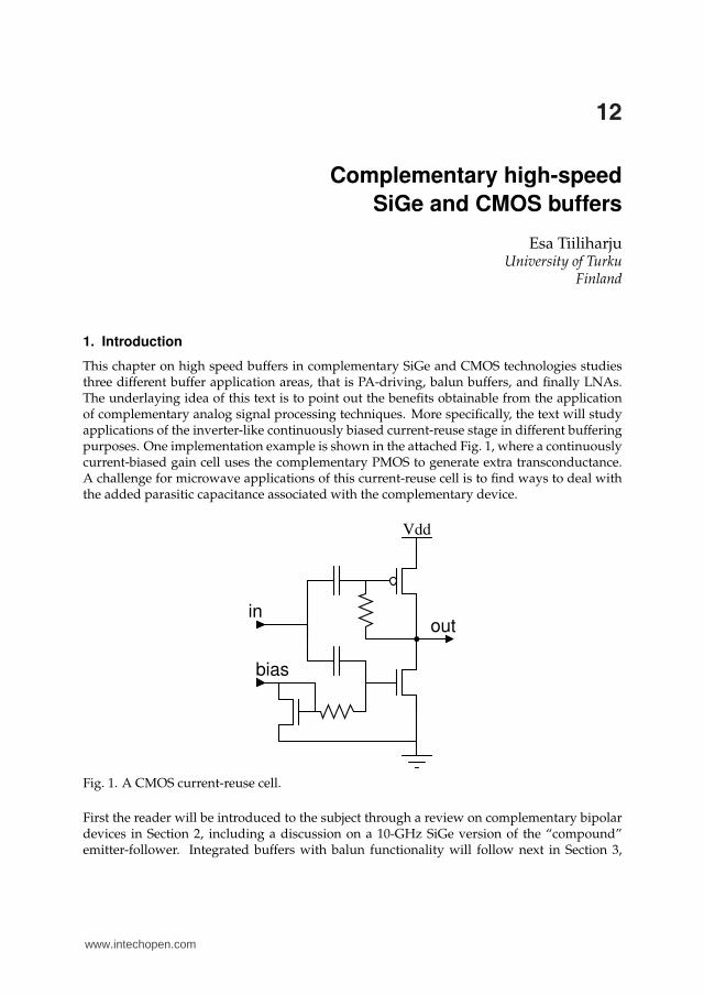
Fig. 8. Cascaded differential pairs used as a balun by Altes et al. (1986).
IN
Out2
Out1
Fig. 9. The CGCS-balun principle developed by Kawashima et al. (2003).
Bruccoleri et al. (2002), a technique which has recently been favored by the UWB design com-munity.
3.3 Single-transistor phase-splitters
Usually, single-transistor phase-splitters have too much phase error as a result of circuit par-asitics. Fig. 10 depicts an example of a single transistor balun, where FET drain and sourcenodes are used as outputs; as is well-known, the inverting (drain) and non-inverting (source)node impedances differ substantially. The impedance seen at the drain node is formed by theparallel connection of the channel conductance go and several parasitic capacitances, such asthe gate-to-drain Cgd, and drain-to-bulk Cdb capacitances. In contrast, the device transcon-ductance gm seen at the source node is in most cases so high that it dominates circuit sourceimpedance estimates. This inherent imbalance has a deleterious effect on the performanceof a single FET circuit as a balun, and the reported ∆A=1 dB (gain error) and φ=176 (phasedifference) values by Koizumi et al. (1995) are in agreement with this, as these simulated re-
www.intechopen.com

Advanced Microwave Circuits and Systems236
RLRg
RL
INOut1
Out2
Fig. 10. One FET as a balun by Koizumi et al. (1995).
Out+
Out−
IN
vgc
Fig. 11. Cross-connected FETs correct single FET balun response by Goldfarb et al. (1994).
sults were reported as best possible for a single FET balun optimized for use in a PersonalCommunication Systems (PCS) application at 950 MHz.
www.intechopen.com

Complementary high-speed SiGe and CMOS buffers 237
V1
V2
V1
V2
V1
V2
Vdd
Out1 Out2In
Fig. 12. One of the few balun amplifiers which exploits complementary circuit techniquesmade by Tripodi & Brekelmans (2007).
To correct the inherent imbalance of the single FET balun, Goldfarb et al. (1994) proposed theuse of a pair of cross-connected correcting transistors, as shown in Fig. 11. However, this is nota promising candidate for a broadband balun solution, for two reasons: 1) seven integratedcapacitors (excluding output buffering) are needed to make it work, so there is an increasein IC area and a great deal of parasitic capacitance involved, and 2) for better balance eachtransistor should have equal gain from the gate to the source/drain terminals: this limits thetopology to use in low-gain applications. The combination of these two points does not implygood broadband performance for this topology, but the reported simulated gain and phasevalues from 1 GHz to 2 GHz support claims for improved accuracy: ∆A=-0.2 dB and φ=178.
3.4 Inverter balun amplifier
CMOS inverters have been succesfully used to implement a balun variable gain amplifier(VGA) LNA for handheld mobile-TV applications by Tripodi & Brekelmans (2007). Schematicof this 90-nm CMOS LNA is shown in Fig. 12, and its use of inverters as gain stages hassimilarities with the feedback amplifier proposed by the author later in this chapter. However,important differences exist such as: a) biasing current control in Fig. 12 has been realizedusing the back-gate biasing voltages V1 and V2, b) use of a series-connected resistor has beenavoided by the author to keep NF low, and c) the amplifier shown does not use a globalfeedback but uses local inverter stage feedback resistors instead. Tabulated results for thisand the other baluns of this section in Table 2 miss many of the fine characteristics such asthe rather low NF=2.5 dB realized for this low-noise VGA, but reference to the table is still anapproapriate conclusion for this section and a fitting preliminary to the next section on LNAs.Based on the table, it is good to point out that well-used complementary stages not only givethe best dynamic range performance but they also produce comparable functionality for mostapplications.
4. CMOS Low-noise amplifiers
It was long widely believed that short-channel CMOS application in high-speed low-noiseamplifiers (LNA) would not be successful, as these devices have a higher than usual excessnoise factor γ. However, that belief has been shown premeditated, first with sub-1dB noise fig-ure LNA implementations for narrowband applications, then with emerging ultra-wideband(UWB) LNAs. Since ultra-wideband (UWB) technologies are currently gaining acceptance
www.intechopen.com
Advanced Microwave Circuits and Systems238
also in European standardization bodies, this niche of communications is under active devel-opment worldwide.Nevertheless, before plunging forward it is approapriate to limit our broadband LNA discus-sion to inductorless fully integrated designs according to the general layout of this chapter. Itis also necessary to mention two specific items of interest: 1) the term LNA will be limited tolow-noise amplifiers which have a gain higher than 10 dB, preferably more, and 2) noise fig-ures are only acceptable in the band where the circuit’s input has been matched to 50 Ω. Thefirst item stems from the very function of any LNA as defined by the Friis’s formula: a low-noise amplifier has to have sufficient gain to isolate and to improve system noise figure, i.e.,to make its own low NF the dominating factor in the system NF. The second item stems fromthe fact that it is trivial to achieve near GaAs-like NF-performances with large WL-area CMOStransistors which have not been matched to 50 Ω, but this is a bit unrealistic, as applicationsusually dictate mandatory matching to 50 Ω.This section will first discuss existing feedback LNA solutions, then performance enhancingdesign techniques such as noise-canceling and current-reuse inputs will be presented, and thissection will be concluded with implementation detail on an LNA by the author which usescurrent-reuse gain-stages in combination with a semi-active dual feedback loop to achieve lownoise, high gain and good isolation in a 130-nm bulk digital CMOS technology.
Vdd
Level
shift
VB
in
out
(a)
Vdd
in
out
Vdd Vdd
Vdd
(b)
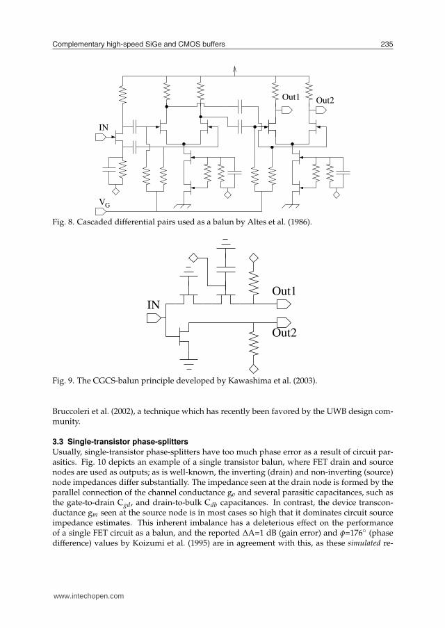
Fig. 13. Two noteworthy feedback LNAs.
4.1 Feedback LNAs
For economical reasons a bulk CMOS process mainly intended for integration of digital cir-cuitry should be used for the purpose of implementing LNAs. Sufficient bandwidth with littlegain variation could be guaranteed with three alternative techniques: 1) distributed amplifi-cation, 2) use of a complex filtering network at circuit input/output, or 3) feedback amplifica-tion. First choice is generally limited by its higher power dissipation and possibly intensive
www.intechopen.com

Complementary high-speed SiGe and CMOS buffers 239
design effort, whereas the second choice includes an increased IC area, high design effort andresistive losses from parasitics. These considerations therefore suggest use of the third alter-native, where a feedback network is used to swap amplifier gain for a wideband frequencyresponse. Advantageously, this stabilizes gain and port impedances as well, and this well-known technology is compatible with low-cost integration in digital CMOS.However, the amount of applicable feedback is limited by stability considerations, and this hastraditionally been dealt with by using different compensation networks which aim at incresingthe amount of available stable feedback. Conventional microwave feedback designs use com-plex compensating capacitor networks for the purpose, but this approach is area-consuming,sensitive to parasitics, and time-consuming to design. An example of a very complex feed-back network is seen in Fig. 13(a) which is the single-stage UWB low-noise amplifier (LNA)design reported by Zhan & Taylor (2006). This high-performance low-noise amplifier (LNA)in 90-nm CMOS achieved inspiring performance with a best possible NF=2.5 dB performanceover the UWB bands. However, this particular implementation uses a 2.5-V supply voltage,and is therefore really not applicable for designs in standard digital CMOS as these use 1.2-Vfor 130-nm and as low as 1.0-V supplies for newer process nodes, as its use of stacked transis-tors limits the available dynamic range (DR), and its complex feedback network requires aninvolved design effort. Fundamentally limiting is the low intrinsic gain of digital transistors,which decreases a single stage gain to an unacceptably low level.A possible alternative which uses three cascaded gain stages is shown in Fig. 13(b) as reportedby Janssens et al. (1997), where the main idea is to improve isolation of the circuit by drivinga resistive feedback network with a gain stage. The circuit in Fig. 13(b) is in fact a variationof a well-known bipolar amplifier connection where an emitter-follower is used to drive thefeedback resistors connected to the input port. However, although the depicted connectionis simple on the surface, its use for e.g. UWB applications is problematic as the feedbackamplifier gain roll-off introduces difficult high frequency poles to the single feedback circuit.As a testimony to this the original circuit shown in Fig. 13(b) uses two additional impedancenetworks at its input to compensate for parasitic effects: an inductor and its dc-block havebeen applied to null parasitics, and a resistor-capacitor (RC) network has also been applied toensure stability.
Vdd
Bias
Out
N1
M1
In
M2
Fig. 14. A noise-canceling stage implementation with biasing details omitted for clarity.
www.intechopen.com

Advanced Microwave Circuits and Systems240
4.2 Noise-canceling LNAs
A very popular broadband low-noise amplifier technique was proposed by Bruccoleri et al.(2002) to break the connection between input resistive matching and noise figure by exploitingtwo feedforward paths for the input-referred noise with matching transfer characteristics butopposite signs. A better understanding of the technique is possible with reference to Fig. 14,where the inverting noise feedforward path is via NMOS transistor M1, whereas the non-inverting noise path is via NMOS transistor M2. According to inventors, the trick here is thatnoise in nodes In and N1 is in-phase as the same noise current flows through the feedbackresistor R to the source impedance Rs (not shown). This is in contrast to signal phase, whichgets inverted by the input stage, and therefore adds at circuit output.Originally reported performance supports the proposed noise-canceling theory, as sub-2dBNF values with matched input have been reported in the band of 250-1100 MHz with goodall-around performance. This performance is limited by the accuracy by which the two oppo-site phasing noise feedforward paths match both in magnitude and phase domain. Indeed,later implementations for higher frequencies tend to show worse NF value performance, e.g.,best noise-canceling ultra-wideband LNAs reported in 2006-2007 (tabulated in the last sub-section in Table 3) reach NF values of 2.7-5.5 dB. To understand this drop from expected lowNF performance in many cases, it should be noted that matching of the two noise feedfor-ward paths comes increasingly difficult at higher frequencies. Also use of nanometer CMOSdevices, which have high channel conductances, makes it difficult to hold on to the assump-tion that M2 acts as a perfect 1/1 voltage-follower. Significance of this is better understoodif the original matching condition is re-printed with the channel conductances taken into ac-count:
AM1 = AM2 ⇐⇒gm1
gm2 + gd2=
(
1 +R
Rs
)
gm2
gm2 + gd2, (2)
where AM(1,2) are FET M1 and M2 associated signal path gains, gm(1,2) are FET transcon-ductances, gd2 represents all impedances at the output node, and the feedback and sourceimpedance have been labeled as R and Rs, respectively.A simple practical interpretation for this matching condition is as follows: since gain is neededto make the LNA noise performance the dominant one, both paths need to have a medium-to-high gain, a condition which dictates matching of a source-follower M2 transfer functionwith that of a common-source stage M1, including its Miller capacitance. This is clearly a verydemanding task for broadband amplifiers.Therefore, rest of the chapter will discuss possibilities to overcome feedback stability prob-lems so as to fully utilize cascaded current-reuse amplifiers’ gain in an ultra-wideband LNAapplication. This approach is somewhat prone to dissipate higher currents, but its applicationband should increase in direct relation to decreasing parasitics, i.e., this approach should scalewell for nanometer CMOS use.
4.3 Current-reuse LNA with semi-active feedback
This section proposes a current-reuse LNA implementation with a semi-active dual feedbackloop as reported by the author in (Tiiliharju & Koivisto (2008)) for the lower UWB band. Theproposed LNA topology scalability to nanometer CMOS processes is good, and as a proof-of-concept it has been integrated in a 130-nm digital CMOS process. The proposed LNA can bemass-produced at a negligible cost with extremely small die area, as it utilizes an area-savinginductorless topology. Furthermore, its novel feedback stage improves isolation, increasesstability, and slightly improves circuit noise performance with no discernible extra cost.
www.intechopen.com

Complementary high-speed SiGe and CMOS buffers 241
in outA1 A2 A3
Afbk
Rfbk
N1
Fig. 15. Proposed feedback network application in a cascade amplifier.
Vdd
vb1 vb2 vb3
inout
Vdd
C1
C2
C3
C4
C5
C6
Rb1 Rb2 Rb3
R1 R2 R3
Rfbk
Afbk
A1 A2 A3
N1
M1
M2
M3
M4
M5
M6
Fig. 16. Transistor level realization of the proposed feedback network application in an UWBLNA.
4.3.1 Design and Architecture
Generally the amount of applicable feedback is limited by stability considerations, but theamount of available stable feedback can be increased by using an active stage Afbk to feedoutput signaling back to a first internal node N1 at the output of the first amplifier stage A1of the cascade A1-A3, and also to its input port via a resistor connection as shown in Fig. 15.A copy of the last amplifier stage, or part thereof, could be used as the proposed active feed-back stage as this allows accurate setting of the amount of feedback used by simple scalingof said dc-connected feedback stage. The proposed use of a copy of the last amplifier stageis the key behind increased amount of stable feedback available, as this inherently realizesfrequency compensation by duplicating single amplifier pole and zero locations. Thus thewell-known stability condition reported by Sedra & Smith (2003), which denies exceeding a20-dB difference between the slopes of the amplifier and feedback frequency response curves
www.intechopen.com

Advanced Microwave Circuits and Systems242
at the point of their Bode-plot intersection is naturally easier to meet. This preferred embodi-ment also avoids prior art (Janssens et al. (1997)) problem of loading the amplifier input portwith feedback amplifer poles and zeros, and the designer can opt for the added flexibility oftwo feedback paths by realizing part of the desired feedback with a feedback resistor Rfbk,which is connected between the cascade amplifier input and output ports. Isolation is alsoincreased and noise slightly decreased, since feedback resistor Rfbk values can be made largeror practically infinite for the same amount of feedback. This is a direct consequence of thesmaller amount of feedback which has to be realized resistively for a given desired amount offeedback.Fig. 16 shows proposed transistor-level realization of the wideband cascade amplifier imple-mentation wherein feedback network (Afbk, Rfbk) has been arranged to trade signal gainarising from the three amplifying stages A1-A3 to a wideband frequency response. Technol-ogy used for this implementation is a bulk 130-nm digital CMOS process with optional MIMcapacitors used for dc-blocking, and a nominal supply of 1.2 volts. High-speed transistorswith low threshold voltages at VTN0=380 mV for NMOS, and VTP0=-390 mV for PMOS vari-ants have been used to build the three near identical core amplifier blocks A1, A2, and A3. Allcapacitors are 1.25-pF integrated MIMs except input capacitor C2 which has been realized asan off-chip capacitor. Local feedback and biasing resistors R1 and R3 at the input and outputbuffering amplifiers A1 and A3 have been set at a low value of 400 Ω to improve input matchand to linearize the device at its output, whereas the second stage local feedback resistor R2has been set to 1200 Ω to increase gain. Transistor M1-M6 areas have been set quite high tokeep the noise figure floor of each stage at a low value; thus 16 × 8µm/0.13µm has been givento each device, notwithstanding whether the device in question is a N- or a PMOS transistor.Traditionally PMOS-transistors with similar channel lenghts L were allocated as much as threetimes the channel width W of their NMOS counterparts, but to cut down circuit parasitics thisapproach has now been avoided.Based on previous knowledge and simulations each 8-µm wide unit transistor has been re-alized in 4 fingers, as this configuration should help to minimize noise by keeping chan-nel resistances at bay. The biasing resistors Rb1, Rb2, and Rb3 have no effect on broad-band noise figure, as they have been given a high value at 9.2 kΩ to exclude biasingchain from signal path and maximize gain. The feedback network devices have been set atAfbk=8µm/0.13µm/PMOS, and Rfbk=1.2 kΩ.
4.3.2 Simulated performance
The advantages of the proposed feedback network show more clearly with increasingamounts of feedback. To demonstrate this Fig. 17 depicts simulation results for two feed-back amplifiers which trade gain from identical similarly biased core amplifiers for extendedbandwidths at ca. 9 GHz with equal remaining 15-dB midband/dc-gains. Thus both ampli-fiers use a similar amount of feedback with the results simulated for the proposed dual-loopfeedback ticked with ⋄. Results simulated for the prior-art resistive-only feedback amplifierhave been ticked with , respectively.Upper sub-picture of Fig. 17 depicts voltage gains for the amplifiers. Small-signal simulationallows extraction of gain as circuit output voltages (VDB(out)), as a (1-Vp∼0 dB) input sig-nal can be used without distortion effects. The plotted data is used to compare peaking nearamplifier 3-dB points, where application of the present invention is shown to reduce peakingnoticeably for this 15-dB amplifier example. To put this result in perspective two things willbe disclosed next: 1) with different element values of the feedback network the improvement
www.intechopen.com

Complementary high-speed SiGe and CMOS buffers 243
in out
Fig. 17. Simulated comparison of feedback techniques (proposed active feedback=⋄, prior artresistive-only=) show a) voltage gain peaking near amplifier 3-dB points, and b) amplifierisolation performances.
Fig. 18. Microphotograph of the realized UWB LNA shows an active area of 193µm×124µm.
obtainable can be increased to ca. 3 dB for this 15-dB amplifier example; and 2) when feedbackis increased to produce over 10-GHz bandwidths at 13-dB midband voltage gains, simulationresults for the resistor-only feedback amplifier indicate instability whereas the proposed circuitmaintains stable behavior. Lower sub-picture of Fig. 17 compares simulated two-port isola-
www.intechopen.com

Advanced Microwave Circuits and Systems244
tion parameters S12 for the implemented 15-dB amplifiers with a clear 7-dB improvementindicated for the proposed feedback network technology.Simulated characteristics for the implemented LNA in Fig. 16 at the nominal biasing point of14.5 mA from a 1.2-V supply predicts good performance: midband gain is 23.7 dB, bandwidth(BW) reaches 7.2 GHz with good input matching of S11=-20.8 dB at 4 GHz. Simulated noisefigures remain below 2.3 dB, and LNA figure-of-merit (FOM) characteristics peaks at 23. TheFOM has been used as defined by Borremans et al. (2007):
FOM = 20 log10
(
Gain(real) BW(GHz)
Power(mW) (NF(real)− 1)
)
, (3)
where Gain stands for insertion gain S21, BW for amplifier 3-dB bandwidth (in GHz), Powerstands for DC power dissipated by the circuit (in milliwatts), and NF is the noise figure givenas a real number, i.e., the noise factor of the circuit.
Fig. 19. Comparison of measured and simulated insertion gain (S21) and isolation (S12) valuesat the 1.2-V biasing point Tiiliharju & Koivisto (2009) (© 2009 IEEE).
4.3.3 Experimental results
The circuit has been tested in nominal conditions using a supply voltage of 1.2 volts, and abiasing current of 14.5 mA. Testing of the IC shown in Fig. 18 has been done using co-planarwafer probes with a pitch of 150 µm. Measured frequency response performance has beencompared to simulated values in Figs. 19-20. Latter of the figures also shows that matchingperformance is acceptable up to ca. 3 GHz as input return loss values stay below -10 dB.However, the depicted measured values differ from the simulated ones, and this is also seenfrom tabulated characteristics in Table 3 where noise figures topping 4 dB have been recordedtogether with |S11|=7 dB as measured at 4 GHz. The 2-dB NF-value increase from the sim-ulated ones has been verified up to 5 GHz at the three different tabulated operating points,and the measured results have been depicted in Fig. 21. An extra low-noise instrumentationamplifier has been used to drive the spectrum analyzer during the noise measurements as
www.intechopen.com

Complementary high-speed SiGe and CMOS buffers 245
Fig. 20. Comparison of measured and simulated input return loss values at the 1.2-V biasingpoint Tiiliharju & Koivisto (2009) (© 2009 IEEE).
Tech. Gain BW S11NF IIP3 freq. VDD Power Area FOM Type Ref.expl.
CMOS dB GHz dB dB dBm GHz V mW mm2
130-nm 20 4.9 -7 4.2 -13 4 1.2 17.4 0.0239 5 feedback This work
19.4 4.5 -7 4.1 -13 1 12.3 6.4
17.8 4 -6 5.9 -15 0.8 7.9 2.7
90-nm 25 0.5-8.2 -7 2 -11 4 2.5 39.0 0.025 15.6 feedback Zhan & Taylor (2006)
130-nm 17 1-7 -10 2.7 -4 3 1.4 25.1 0.019 5.9 noise cancel Ramzan et al. (2007)
90-nm 15.3 0-6 -10 3.7 NA 4 1 3.4 0.0017 17.7 feedback Borremans et al. (2007)
90-nm 24 0.5-6.2 -15 2.7 -5 4 2.7 42.0 0.016 7.9 feedback Perumana et al. (2007)
65-nm 15.6 0.2-5.2 -13 3.2 3 4 1.2 21.0 0.01 2.4 noise cancel Blaakmeer et al. (2007)
90-nm 12 2-11 -10 5.5 -4 4 1.2 17.0 0.7 -2 noise cancel Wang & Wang (2006)
Table 3. Comparison of LNA performances.
this increases reliability of the Y-parameter noise measurements. The measurement setup hasalso been verified by measuring another amplifier with known noise performance. All othermeasurements have been done unbuffered, i.e., the proposed LNA has been used to directlydrive the equipment.The plotted NF data together with the recorded gains hints at a layout error at amplifier in-put, as any noisy resistive parasitics at the LNA output should be masked by its high gain.Nevertheless, the proposed amplifier FOM-performance compares well to state-of-the-art, asit peaks at the 1.0-V biasing point at 6.4. Only one design uses such a low supply voltage, butthis has been realized with a more advanced process node. Measured frequency responsesat all biasing points shown in Fig. 22 also confirms the claims on stability and good isola-tion. Only a uniform gain decrease has been recorded with lowering supply voltages, with nodiscernible degradation in isolation or peaking at passband edge.
www.intechopen.com

Advanced Microwave Circuits and Systems246
Fig. 21. Comparison of measured NF performance at the 1.2-V, 1.0-V and 0.8-V biasing points.
Fig. 22. Comparison of measured insertion gain (S21) and isolation (S12) performances at the1.2-V, 1.0-V and 0.8-V biasing points.
5. Summary and future work
Successful applications of complementary signal processing to microwave buffers have beenstudied in this chapter with special emphasis on CMOS. This approach is justified by CMOSscaling to the nanometer domain, which makes it possible to use this very economical tech-nology in the microwave domain. However, first section has elaborated on a complementarybipolar process and its possible application for basestation buffering purposes, an applicationwhich is perhaps better served with this high-voltage process. Second section has discussed
www.intechopen.com

Complementary high-speed SiGe and CMOS buffers 247
integrated baluns, which naturally has taken this text to the third section on LNAs where dif-ferent topologies compatible with modern nanoscale CMOS technologies have been studied.To summarize, it seems that there is a substantial benefit in using complementary analog sig-nal processing techniques, however, parasitics compensation is a demanding design task inthe higher operating bands.
6. References
Altes, S. K., Chen, T.-H. & Ragonese, L. J. (1986). Monolithic RC all-pass networks withconstant-phase-difference outputs, IEEE Trans. Microw. Theory Tech. 34(12): 1533–1537.
Blaakmeer, S. C., Klumperink, E. A. M., Nauta, B. & Leenaerts, D. M. W. (2007). An inductor-less wideband balun-LNA in 65nm CMOS with balanced output, 33rd European SolidState Circuits Conference, 2007. ESSCIRC, pp. 364–367.
Borremans, J., Wambacq, P. & Linten, D. (2007). An ESD-protected DC-to-6GHz 9.7mW LNAin 90nm digital CMOS, Solid-State Circuits, 2007 IEEE International Conference Digestof Technical Papers, pp. 422–423, 613.
Bruccoleri, F., Klumperink, E. A. M. & Nauta, B. (2002). Noise cancelling in wideband CMOSLANs, Solid-State Circuits Conference, 2002. Digest of Technical Papers. ISSCC. 2002 IEEEInternational, Vol. 2, pp. 330–533.
Davis, P. C., Moyer, S. F. & Saari, V. R. (1974). High slew rate monolithic operational amplifierusing compatible complementary P-N-P’s, IEEE J. Solid-State Circuits 9(6): 340–347.
El-Kareh, B., Balster, S., Leitz, W. andSteinrnannl, P., Yasudal, H., Corsi, M., Dawoodi, K.,Dirnyke, C., Foglietti, P., Haeusle, A., Menz, P., Ramin, M., Schamagl, T., Schiekofe,M., Schober, M., Schulz, U., Swanson, L., Tatman, D., Waitschul, M., Weijtmans, J.& Willis, C. (2003). A 5 V complementary-SiGe BiCMOS technology for high-speedprecision analog circuits, Bipolar/BiCMOS Circuits and Technology Proceedings of the2003 Meeting, IEEE, pp. 211–214.
Fong, K. L. & Meyer, R. G. (1998). High-frequency nonlinearity analysis of common-emitterand differential-pair transconductance stages, IEEE J. Solid-State Circuits 33(4): 548–555.
Gilbert, B. (1997). The MICROMIXER: A highly linear variant of the gilbert mixer using abisymmetric Class-AB input stage, IEEE Journal of Solid-State Circuits 32(9): 1412–1423.
Goldfarb, M., Cole, J. & Platzker, A. (1994). A novel MMIC biphase modulator with variablegain using enhancement-mode FETS suitable for 3 V wireless applications, Microwaveand Millimeter-Wave Monolithic Circuits Symposium, 1994. Digest of Papers., Vol. I, IEEE,pp. 99–102.
Janssens, J., Steyaert, M. & Miyakawa, H. (1997). A 2.7 Volt CMOS broadband low noiseamplifier, VLSI Circuits, 1997. Digest of Technical Papers., 1997 Symposium on, pp. 87–88.
Kawashima, M., Nakagawa, T. & Araki, K. (2003). A novel broadband active balun, 33rdEuropean Microwave Conference, München, Germany, pp. 495–498.
Kobayashi, K. W. (1996). A novel HBT active transformer balanced Schottky diode mixer, IEEEMTT-S International Microwave Symposium Digest, Vol. 2, IEEE, pp. 947–950.
Koizumi, H., Nagata, S., Tateoka, K., Kanazawa, K. & Ueda, D. (1995). A GaAs single bal-anced mixer MMIC with built-in active balun for personal communication systems,
www.intechopen.com

Advanced Microwave Circuits and Systems248
Microwave and Millimeter-Wave Monolithic Circuits Symposium, 1995. Digest of Papers.,IEEE, pp. 77–80.
Ma, H., Fang, S. J., Fujiang, L. & Nakamura, H. (1998). Novel active differential phase splittersin RFIC for wireless applications, IEEE Trans. Microw. Theory Tech. 46(12): 2597–2603.
Monticelli, D. (2004). The future of complementary bipolar, Bipolar/BiCMOS Circuits and Tech-nology Proceedings of the 2004 Meeting, IEEE, pp. 21–25.
Perumana, B. G., Zhan, J.-H. C., Taylor, S. S. & Laskar, J. (2007). A 5 GHz, 21 dBm output-IP3resistive feedback LNA in 90-nm CMOS, 33rd European Solid State Circuits Conference,2007. ESSCIRC, pp. 372–375.
Peters, L. (2004). NBTI: A growing threat to device reliability, Semiconductor international .Ramzan, R., Andersson, S., Dabrowski, J. & Svensson, C. (2007). A 1.4V 25mW inductorless
wideband LNA in 0.13µm CMOS, Solid-State Circuits, 2007 IEEE International Confer-ence Digest of Technical Papers, pp. 424–425, 613.
Sedra, A. S. & Smith, K. C. (2003). Microelectronic Circuits, fifth edn, Oxford University Press.Tiiliharju, E. & Halonen, K. (2005). Active differential broadband phase-splitter for
quadrature-modulator applications, Microwave Theory and Techniques, IEEE Transac-tions on 53(2): 679–686.
Tiiliharju, E. & Koivisto, T. (2008). Feedback network for cascaded ultra-wideband amplifiers,Ultra-Wideband, 2008. ICUWB 2008. IEEE International Conference on, Vol. 1, pp. 21–24.
Tiiliharju, E. & Koivisto, T. (2009). A dual feedback loop low-noise amplifier, Proceedings of the27th Norchip Conference, Trondheim, Norway, pp. xxx–xxx. submitted to be accepted.
Tiiliharju, E. & Pellikka, H. (2007). Complementary bipolar devices for base station applica-tions, Proceedings of the 2007 IEEE International Microwave Symposium (IMS-07), IEEE,Honolulu, Hawaii, USA, pp. 263–266.
Tiiliharju, E., Pellikka, H. & Halonen, K. (2006). A current re-use mixer and a push-pull bufferfor base station applications, IEEE Microw. Wireless Compon. Lett. 16(9): 514–516.
Tripodi, L. & Brekelmans, H. (2007). Low-noise variable-gain amplifier in 90-nm CMOS for TVon mobile, 33rd European Solid State Circuits Conference, 2007. ESSCIRC, pp. 368–371.
Wang, C.-S. & Wang, C.-K. (2006). A 90nm CMOS low noise amplifier using noise neutraliz-ing for 3.1-10.6GHz UWB system, Solid-State Circuits Conference, 2006. ESSCIRC 2006.Proceedings of the 32nd European, pp. 251–254.
Zhan, J.-H. C. & Taylor, S. S. (2006). A 5GHz resistive-feedback CMOS LNA for low-cost multi-standard applications, Solid-State Circuits, 2006 IEEE International Conference Digest ofTechnical Papers, pp. 721–722, 730.
www.intechopen.com

Advanced Microwave Circuits and SystemsEdited by Vitaliy Zhurbenko
ISBN 978-953-307-087-2Hard cover, 490 pagesPublisher InTechPublished online 01, April, 2010Published in print edition April, 2010
InTech EuropeUniversity Campus STeP Ri Slavka Krautzeka 83/A 51000 Rijeka, Croatia Phone: +385 (51) 770 447 Fax: +385 (51) 686 166www.intechopen.com
InTech ChinaUnit 405, Office Block, Hotel Equatorial Shanghai No.65, Yan An Road (West), Shanghai, 200040, China
Phone: +86-21-62489820 Fax: +86-21-62489821
This book is based on recent research work conducted by the authors dealing with the design anddevelopment of active and passive microwave components, integrated circuits and systems. It is divided intoseven parts. In the first part comprising the first two chapters, alternative concepts and equations for multiportnetwork analysis and characterization are provided. A thru-only de-embedding technique for accurate on-wafer characterization is introduced. The second part of the book corresponds to the analysis and design ofultra-wideband low- noise amplifiers (LNA).
How to referenceIn order to correctly reference this scholarly work, feel free to copy and paste the following:
Esa Tiiliharju (2010). Complementary High-Speed SiGe and CMOS Buffers, Advanced Microwave Circuits andSystems, Vitaliy Zhurbenko (Ed.), ISBN: 978-953-307-087-2, InTech, Available from:http://www.intechopen.com/books/advanced-microwave-circuits-and-systems/complementary-high-speed-sige-and-cmos-buffers

© 2010 The Author(s). Licensee IntechOpen. This chapter is distributedunder the terms of the Creative Commons Attribution-NonCommercial-ShareAlike-3.0 License, which permits use, distribution and reproduction fornon-commercial purposes, provided the original is properly cited andderivative works building on this content are distributed under the samelicense.