
COMPARISON OF THE MOSFET AND THE BJT - OUP · COMPARISON OF THE MOSFET AND THE BJT In this appendix...
19
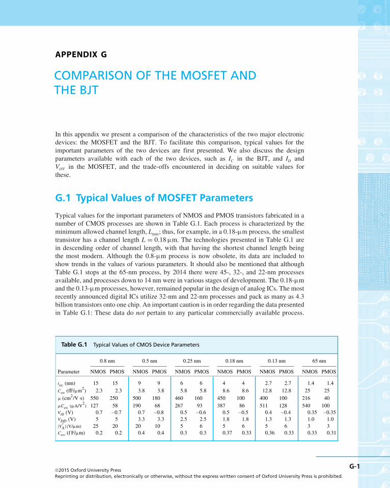
APPENDIX G COMPARISON OF THE MOSFET AND THE BJT In this appendix we present a comparison of the characteristics of the two major electronic devices: the MOSFET and the BJT. To facilitate this comparison, typical values for the important parameters of the two devices are first presented. We also discuss the design parameters available with each of the two devices, such as I C in the BJT, and I D and V OV in the MOSFET, and the trade-offs encountered in deciding on suitable values for these. G.1 Typical Values of MOSFET Parameters Typical values for the important parameters of NMOS and PMOS transistors fabricated in a number of CMOS processes are shown in Table G.1. Each process is characterized by the minimum allowed channel length, L min ; thus, for example, in a 0.18-μm process, the smallest transistor has a channel length L = 0.18 μm. The technologies presented in Table G.1 are in descending order of channel length, with that having the shortest channel length being the most modern. Although the 0.8-μm process is now obsolete, its data are included to show trends in the values of various parameters. It should also be mentioned that although Table G.1 stops at the 65-nm process, by 2014 there were 45-, 32-, and 22-nm processes available, and processes down to 14 nm were in various stages of development. The 0.18-μm and the 0.13-μm processes, however, remained popular in the design of analog ICs. The most recently announced digital ICs utilize 32-nm and 22-nm processes and pack as many as 4.3 billion transistors onto one chip. An important caution is in order regarding the data presented in Table G.1: These data do not pertain to any particular commercially available process. Table G.1 Typical Values of CMOS Device Parameters 0.8 nm 0.5 nm 0.25 nm 0.18 nm 0.13 nm 65 nm Parameter NMOS PMOS NMOS PMOS NMOS PMOS NMOS PMOS NMOS PMOS NMOS PMOS t ox (nm) 15 15 9 9 6 6 4 4 2.7 2.7 1.4 1.4 C ox (fF/μm 2 ) 2.3 2.3 3.8 3.8 5.8 5.8 8.6 8.6 12.8 12.8 25 25 μ (cm 2 /V· s) 550 250 500 180 460 160 450 100 400 100 216 40 μC ox (μA/V 2 ) 127 58 190 68 267 93 387 86 511 128 540 100 V t 0 (V) 0.7 −0.7 0.7 −0.8 0.5 −0.6 0.5 −0.5 0.4 −0.4 0.35 −0.35 V DD (V) 5 5 3.3 3.3 2.5 2.5 1.8 1.8 1.3 1.3 1.0 1.0 |V A | (V/μm) 25 20 20 10 5 6 5 6 5 6 3 3 C ov (f F/μm) 0.2 0.2 0.4 0.4 0.3 0.3 0.37 0.33 0.36 0.33 0.33 0.31 G-1 ©2015 Oxford University Press Reprinting or distribution, electronically or otherwise, without the express written consent of Oxford University Press is prohibited.
Transcript of COMPARISON OF THE MOSFET AND THE BJT - OUP · COMPARISON OF THE MOSFET AND THE BJT In this appendix...
APPENDIX G
COMPARISON OF THE MOSFET ANDTHE BJT
In this appendix we present a comparison of the characteristics of the two major electronicdevices: the MOSFET and the BJT. To facilitate this comparison, typical values for theimportant parameters of the two devices are first presented. We also discuss the designparameters available with each of the two devices, such as IC in the BJT, and ID andVOV in the MOSFET, and the trade-offs encountered in deciding on suitable values forthese.
G.1 Typical Values of MOSFET Parameters
Typical values for the important parameters of NMOS and PMOS transistors fabricated in anumber of CMOS processes are shown in Table G.1. Each process is characterized by theminimum allowed channel length, Lmin; thus, for example, in a 0.18-μm process, the smallesttransistor has a channel length L = 0.18μm. The technologies presented in Table G.1 arein descending order of channel length, with that having the shortest channel length beingthe most modern. Although the 0.8-μm process is now obsolete, its data are included toshow trends in the values of various parameters. It should also be mentioned that althoughTable G.1 stops at the 65-nm process, by 2014 there were 45-, 32-, and 22-nm processesavailable, and processes down to 14 nm were in various stages of development. The 0.18-μmand the 0.13-μm processes, however, remained popular in the design of analog ICs. The mostrecently announced digital ICs utilize 32-nm and 22-nm processes and pack as many as 4.3billion transistors onto one chip. An important caution is in order regarding the data presentedin Table G.1: These data do not pertain to any particular commercially available process.
Table G.1 Typical Values of CMOS Device Parameters
0.8 nm 0.5 nm 0.25 nm 0.18 nm 0.13 nm 65 nm
Parameter NMOS PMOS NMOS PMOS NMOS PMOS NMOS PMOS NMOS PMOS NMOS PMOS
tox (nm) 15 15 9 9 6 6 4 4 2.7 2.7 1.4 1.4Cox (fF/μm
2) 2.3 2.3 3.8 3.8 5.8 5.8 8.6 8.6 12.8 12.8 25 25μ (cm2/V·s) 550 250 500 180 460 160 450 100 400 100 216 40μCox (μA/V
2) 127 58 190 68 267 93 387 86 511 128 540 100
Vt0 (V) 0.7 −0.7 0.7 −0.8 0.5 −0.6 0.5 −0.5 0.4 −0.4 0.35 −0.35VDD (V) 5 5 3.3 3.3 2.5 2.5 1.8 1.8 1.3 1.3 1.0 1.0|V ′A|(V/μm) 25 20 20 10 5 6 5 6 5 6 3 3
Cov (f F/μm) 0.2 0.2 0.4 0.4 0.3 0.3 0.37 0.33 0.36 0.33 0.33 0.31
G-1©2015 Oxford University PressReprinting or distribution, electronically or otherwise, without the express written consent of Oxford University Press is prohibited.
G-2 Appendix G Comparison of the MOSFET and the BJT
Accordingly, these generic data are not intended for use in an actual IC design; rather, theyshow trends and, as we shall see, help to illustrate design trade-offs as well as enable us towork out design examples and problems with parameter values that are as realistic as possible.
As indicated in Table G.1, the trend has been to reduce the minimum allowable channellength. This trend has been motivated by the desire to pack more transistors on a chip as wellas to operate at higher speeds or, in analog terms, over wider bandwidths.
Observe that the oxide thickness, tox, scales downwith the channel length, reaching 1.4 nmfor the 65-nm process. Since the oxide capacitance Cox is inversely proportional to tox, we seethat Cox increases as the technology scales down. The surface mobility μ decreases as thetechnology minimum-feature size is decreased, and μp decreases faster than μn. As a result,the ratio of μp to μn has been decreasing with each generation of technology, falling fromabout 0.5 for older technologies to 0.2 or so for the newer ones. Despite the reduction ofμn andμp, the transconductance parameters k ′
n =μnCox and k ′p =μpCox have been steadily increasing.
As a result, modern short-channel devices achieve required levels of bias currents at loweroverdrive voltages. As well, they achieve higher transconductance, a major advantage.
Although the magnitudes of the threshold voltages Vtn and Vtp have been decreasing withLmin from about 0.7–0.8 V to 0.3–0.4 V, the reduction has not been as large as that of thepower supply VDD. The latter has been reduced dramatically, from 5 V for older technologiesto 1.0 V for the 65-nm process. This reduction has been necessitated by the need to keepthe electric fields in the smaller devices from reaching very high values. Another reason forreducing VDD is to keep power dissipation as low as possible given that the IC chip now has amuch larger number of transistors.1
The fact that in modern short-channel CMOS processes |Vt| has become a much largerproportion of the power-supply voltage poses a serious challenge to the circuit design engineer.Recalling that |VGS| = |Vt|+|VOV |, whereVOV is the overdrive voltage, to keep |VGS| reasonablysmall, |VOV | for modern technologies is usually in the range of 0.1 V to 0.2 V. To appreciatethis point further, recall that to operate a MOSFET in the saturation region, |VDS| must exceed|VOV |; thus, to be able to have a number of devices stacked between the power-supply rails ina regime in which VDD is only 1.8 V or lower, we need to keep |VOV | as low as possible. Wewill shortly see, however, that operating at a low |VOV | has some drawbacks.
Another significant though undesirable feature of modern deep submicron (Lmin <
0.25μm)CMOS technologies is that the channel-lengthmodulation effect is very pronounced.As a result,V ′
A has decreased to about 3V/μm,which combinedwith the decreasing values ofLhas caused the Early voltage VA = V ′
AL to become very small. Correspondingly, short-channelMOSFETs exhibit low output resistances.
Studying the MOSFET high-frequency2 equivalent-circuit model in Section 10.2 and thehigh-frequency response of the common-source amplifier in Section 10.3 shows that twomajor MOSFET capacitances are Cgs and Cgd . While Cgs has an overlap component,3 Cgd isentirely an overlap capacitance. Both Cgd and the overlap component of Cgs are almost equaland are denoted Cov . The last line of Table G.1 provides the value of Cov per micron of gatewidth. Although the normalized Cov has been staying more or less constant with the reductionin Lmin, we will shortly see that the shorter devices exhibit much higher operating speeds andwider amplifier bandwidths than the longer devices. Specifically, we will, for example, seethat fT for a 0.25-μm NMOS transistor can be as high as 10 GHz.
1Chip power dissipation is a very serious issue, with some ICs dissipating as much as 100W. As a result,an important current area of research concerns what is termed “power-aware design.”2For completeness, this appendix includes material on the high-frequency models and operation of boththe MOSFET and the BJT. These topics are covered in Chapter 10. The reader can easily skip theappendix paragraphs dealing with these topics until Chapter 10 has been studied.3Overlap capacitances result because the gate electrodeoverlaps the source anddrain diffusions (Fig. 5.1).
©2015 Oxford University PressReprinting or distribution, electronically or otherwise, without the express written consent of Oxford University Press is prohibited.

G.2 Typical Values of IC BJT Parameters G-3
G.2 Typical Values of IC BJT Parameters
Table G.2 provides typical values for the major parameters that characterize integrated-circuitbipolar transistors. Data are provided for devices fabricated in two different processes: thestandard, old process, known as the “high-voltage process,” and an advanced,modern process,referred to as a “low-voltage process.” For each processwe show the parameters of the standardnpn transistor and those of a special type of pnp transistor known as a lateral pnp (as opposedto vertical, as in the npn case) (see Appendix A). In this regard we shouldmention that a majordrawback of standard bipolar integrated-circuit fabrication processes has been the lack of pnptransistors of a quality equal to that of the npn devices. Rather, there are a number of pnpimplementations for which the lateral pnp is the most economical to fabricate. Unfortunately,however, as should be evident fromTable G.2, the lateral pnp has characteristics that aremuchinferior to those of the vertical npn. Note in particular the lower value of β and the much largervalue of the forward transit time τF that determines the emitter–base diffusion capacitanceCde and, hence, the transistor speed of operation. The data in Table G.2 can be used to showthat the unity-gain frequency of the lateral pnp is 2 orders of magnitude lower than that ofthe npn transistor fabricated in the same process. Another important difference between thelateral pnp and the corresponding npn transistor is the value of collector current at which theirβ values reach their maximums: For the high-voltage process, for example, this current is inthe tens of microamperes range for the pnp and in the milliampere range for the npn. On thepositive side, the problem of the lack of high-quality pnp transistors has spurred analog circuitdesigners to come up with highly innovative circuit topologies that either minimize the useof pnp transistors or minimize the dependence of circuit performance on that of the pnp. Weencounter some of these ingenious circuits at various locations in this book.
The dramatic reduction in device size achieved in the advanced low-voltage process shouldbe evident fromTableG.2. As a result, the scale current IS also has been reduced by about threeorders of magnitude. Here we should note that the base width,WB, achieved in the advancedprocess is on the order of 0.1μm, as compared to a few microns in the standard high-voltageprocess. Note also the dramatic increase in speed; for the low-voltage npn transistor, τF = 10 psas opposed to 0.35 ns in the high-voltage process. As a result, fT for the modern npn transistoris 10 GHz to 25 GHz, as compared to the 400 MHz to 600 MHz achieved in the high-voltageprocess. Although the Early voltage, VA, for the modern process is lower than its value in the
Table G.2 Typical Parameter Values for BJTs*
Standard High-Voltage Process Advanced Low-Voltage Process
Parameter npn Lateral pnp npn Lateral pnp
AE (μm2) 500 900 2 2IS (A) 5× 10⁻¹⁵ 2× 10⁻¹⁵ 6× 10⁻¹⁸ 6× 10⁻¹⁸
β0 (A/A) 200 50 100 50VA (V) 130 50 35 30VCEO (V) 50 60 8 18τF 0.35 ns 30 ns 10 ps 650 psCje0 1 pF 0.3 PF 5 fF 14 fFCμ0 0.3 pF 1 pF 5 fF 15 fFrx(�) 200 300 400 200
*Adapted from Gray et al. (2001); see Appendix I.
©2015 Oxford University PressReprinting or distribution, electronically or otherwise, without the express written consent of Oxford University Press is prohibited.

G-4 Appendix G Comparison of the MOSFET and the BJT
old high-voltage process, it is still reasonably high at 35 V. Another feature of the advancedprocess—and one that is not obvious fromTable G.2—is that β for the npn peaks at a collectorcurrent of 50μA or so. Finally, note that as the name implies, npn transistors fabricated in thelow-voltage process break down at collector–emitter voltages of 8 V, versus 50 V or so for thehigh-voltage process. Thus, while circuits designed with the standard high-voltage processutilize power supplies of ±15 V (e.g., in commercially available op amps of the 741 type),the total power-supply voltage utilized with modern bipolar devices is 5 V (or even 2.5 V toachieve compatibility with some of the submicron CMOS processes).
G.3 Comparison of Important Characteristics
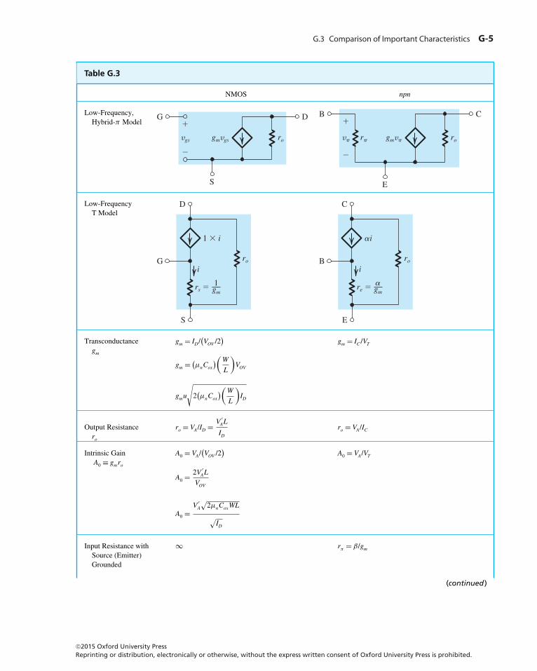
Table G.3 provides a compilation of the important characteristics of the NMOS and the npntransistors. The material is presented in a manner that facilitates comparison. In the following,we comment on the various items in Table G.3. As well, a number of numerical examplesand exercises are provided to illustrate how the wealth of information in Table G.3 can be putto use. Before proceeding, note that the PMOS and the pnp transistors can be compared in asimilar way.
Table G.3 Comparison of MOSFET and the BJT
NMOS npn
Circuit Symbol
iG
iD
vDS
vGD
vGS
��
��
�
�
iC
vCE
vBC
vBE
��
��
�
�
iB
To Operate inthe Active Mode,Two ConditionsHave to BeSatisfied
(1) Induce a channel:
vGS ≥ Vt , Vt = 0.3–0.5V
Let vGS = Vt + vOV
(2) Pinch-off channel at drain:
vGD < Vt
or equivalently,
vDS ≥ VOV , VOV = 0.1–0.3V
(1) Forward-bias EBJ:
vBE ≥ VBEon, VBEon � 0.5V
(2) Reverse-bias CBJ:
vBC < VBCon, VBCon � 0.4V
or equivalently,
vCE ≥ 0.3V
Current–VoltageCharacteristics inthe Active Region
iD = 1
2μnCox
W
L
(vGS −Vt
)2(1+ vDS
VA
)
= 1
2μnCox
W
Lv2OV
(1+ vDS
VA
)
iG = 0
iC = ISevBE /VT
(1+ vCE
VA
)
iB = iC /β
©2015 Oxford University PressReprinting or distribution, electronically or otherwise, without the express written consent of Oxford University Press is prohibited.
G.3 Comparison of Important Characteristics G-5
Table G.3
NMOS npn
Low-Frequency,Hybrid-π Model �
�
vgs
DG
S
rogmvgs
�
�
vp
CB
E
rogmvprp
Low-FrequencyT Model
D
S
G
1 � i
ro
i
rs � 1gm
C
E
B
ai
ro
i
re � agm
Transconductancegm
gm = ID/(VOV /2
)
gm = (μnCox
)(WL
)VOV
gmu
√2(μnCox
)(WL
)ID
gm = IC /VT
Output Resistancero
ro = VA/ID = V ′AL
IDro = VA/IC
Intrinsic GainA0 ≡ gmro
A0 = VA/(VOV /2
)
A0 = 2V ′AL
VOV
A0 =V ′A
√2μnCoxWL√ID
A0 = VA/VT
Input Resistance withSource (Emitter)Grounded
∞ rπ = β/gm
(continued )
©2015 Oxford University PressReprinting or distribution, electronically or otherwise, without the express written consent of Oxford University Press is prohibited.
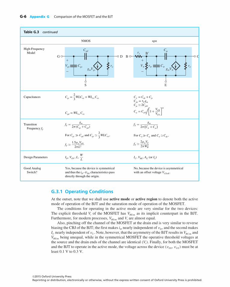
G-6 Appendix G Comparison of the MOSFET and the BJT
Table G.3 continued
NMOS npn
High-FrequencyModel
�
�
Vgs
DG
S
rogmVgs
Cgs
Cgd
�
�
Vp
CB�
B
ro
rx
gmVp
rp Cp
Cm
E
Capacitances Cgs = 2
3WLCox +WLovCox
Cgd =WLovCox
Cπ = Cde +Cje
Cde = τFgmCje � 2Cje0
Cμ = Cμ0
/[1+ VCB
VC0
]m
TransitionFrequency fT
fT = gm2π(Cgs +Cgd)
For Cgs � Cgd and Cgs � 2
3WLCox ,
fT � 1.5μnVOV2πL2
fT = gm2π(Cπ +Cμ
)For Cπ� Cμ and Cπ �Cde,
fT � 2μnVT2πW 2
B
Design Parameters ID, VOV , L,W
LIC , VBE , AE (or IS)
Good AnalogSwitch?
Yes, because the device is symmetricaland thus the iD–vDS characteristics passdirectly through the origin.
No, because the device is asymmetricalwith an offset voltage VCEoff .
G.3.1 Operating Conditions
At the outset, note that we shall use active mode or active region to denote both the activemode of operation of the BJT and the saturation mode of operation of the MOSFET.
The conditions for operating in the active mode are very similar for the two devices:The explicit threshold Vt of the MOSFET has VBEon as its implicit counterpart in the BJT.Furthermore, for modern processes, VBEon and Vt are almost equal.
Also, pinching off the channel of the MOSFET at the drain end is very similar to reversebiasing the CBJ of the BJT; the first makes iD nearly independent of vD, and the second makesIC nearly independent of vC . Note, however, that the asymmetry of the BJT results in VBCon andVBEon being unequal, while in the symmetrical MOSFET the operative threshold voltages atthe source and the drain ends of the channel are identical (Vt). Finally, for both the MOSFETand the BJT to operate in the active mode, the voltage across the device (vDS, vCE) must be atleast 0.1 V to 0.3 V.
©2015 Oxford University PressReprinting or distribution, electronically or otherwise, without the express written consent of Oxford University Press is prohibited.
G.3 Comparison of Important Characteristics G-7
G.3.2 Current–Voltage Characteristics
The square-law control characteristic, iD−vGS, in the MOSFET should be contrasted with theexponential control characteristic, iC−vBE , of the BJT. Obviously, the latter is a much moresensitive relationship, with the result that iC can vary over a very wide range (five decadesor more) within the same BJT. In the MOSFET, the range of iD achieved in the same deviceis much more limited. To appreciate this point further, consider the parabolic relationshipbetween iD and vOV , and recall from our discussion above that vOV is usually kept in a narrowrange (0.1 V to 0.3 V).
Next we consider the effect of the device dimensions on its current. For the bipolartransistor, the control parameter is the area of the emitter–base junction (EBJ), AE , whichdetermines the scale current IS. It can be varied over a relatively narrow range, such as 10 to1. Thus, while the emitter area can be used to achieve current scaling in an IC (as we can seein Section 8.2 in connection with the design of current mirrors), its narrow range of variationreduces its significance as a design parameter. This is particularly so if we compare AE withits counterpart in the MOSFET, the aspect ratioW/L. MOSFET devices can be designed withW/L ratios in a wide range, such as 1.0 to 500. As a result, W/L is a very significant MOSdesign parameter. Like AE , it is also used in current scaling, as we can see in Section 8.2.Combining the possible range of variation of vOV and W/L, one can design MOS transistorsto operate over an iD range of four decades or so.
The channel-length modulation in the MOSFET and the base-width modulation in theBJT are similarly modeled and give rise to the dependence of iD (iC) on vDS (vCE) and, hence,to the finite output resistance ro in the active region. Two important differences, however,exist. In the BJT, VA is solely a process-technology parameter and does not depend on thedimensions of the BJT. In the MOSFET, the situation is quite different: VA = V ′
AL, whereV ′A is a process-technology parameter and L is the channel length used. Also, in modern
deep submicron processes, V ′A is very low, resulting in VA values that are lower than the
corresponding values for the BJT.The last, and perhaps most important, difference between the current–voltage charac-
teristics of the two devices concerns the input current into the control terminal: While atlow frequencies the gate current of the MOSFET is practically zero and the input resistancelooking into the gate is practically infinite, the BJT draws base current iB that is proportionalto the collector current; that is, iB = iC/β The finite base current and the correspondingfinite input resistance looking into the base comprise a definite disadvantage of the BJTin comparison to the MOSFET. Indeed, it is the infinite input resistance of the MOSFETthat has made possible analog and digital circuit applications that are not feasible with theBJT. Examples include dynamic digital memory (Chapter 16) and switched-capacitor filters(Chapter 17).
Example G.1
(a) For an NMOS transistor with W/L = 10 fabricated in the 0.18-μm process whose data are givenin Table G.1, find the values of VOV and VGS required to operate the device at ID = 100 μA. Ignorechannel-length modulation.
(b) FindVBE for an npn transistor fabricated in the low-voltage process specified in Table G.2 and operatedat IC = 100 μA. Ignore base-width modulation.
©2015 Oxford University PressReprinting or distribution, electronically or otherwise, without the express written consent of Oxford University Press is prohibited.
G-8 Appendix G Comparison of the MOSFET and the BJT
Example G.1 continued
Solution
(a)
ID = 1
2
(μnCox
)(WL
)V 2OV
Substituting ID = 100 μA, W/L = 10, and, from Table G.1, μnCox = 387 μA/V2 results in
100 = 1
2× 387× 10×V 2
OV
VOV = 0.23 V
Thus,
VGS= Vtn +VOV = 0.5+ 0.23= 0.73 V
(b) IC = ISeVBE /VT
Substituting IC = 100 μA and, from Table G.2, IS = 6× 10⁻¹⁸ A gives,
VBE = 0.025 ln100× 10−6
6× 10−18 = 0.76 V
EXERCISE
G.1 (a) For NMOS transistors fabricated in the 0.18-μm technology specified in Table G.1, find the rangeof ID obtained for active-mode operation with VOV ranging from 0.2 V to 0.4 V and W/L = 0.1 to 100.Neglect channel-length modulation.(b) If a similar range of current is required in an npn transistor fabricated in the low-voltage processspecified in Table G.2, find the corresponding change in its VBE .Ans. (a) IDmin = 0.8 μA and IDmax = 3.1 mA for a range of about 4000:1; (b) for IC varying over a 4000:1range, �VBE = 207 mV
G.3.3 Low-Frequency Small-Signal Models
The low-frequency models for the two devices are very similar except, of course, for the finitebase current (finite β) of the BJT, which gives rise to rπ in the hybrid-π model and to theunequal emitter and collector currents in the T models α < 1. Here it is interesting to note thatthe low-frequency, small-signal models become identical if one thinks of the MOSFET as aBJT with β = ∞(α = 1)
©2015 Oxford University PressReprinting or distribution, electronically or otherwise, without the express written consent of Oxford University Press is prohibited.
G.3 Comparison of Important Characteristics G-9
For both devices, the hybrid-π model indicates that the open-circuit voltage gain obtainedfrom gate to drain (base to collector) with the source (emitter) grounded is −gmro. It followsthat gmro is themaximum gain available from a single transistor of either type. This importanttransistor parameter is given the name intrinsic gain and is denoted A0. We have more to sayabout the intrinsic gain in Section 8.3.2.
Although not included in the MOSFET low-frequency model shown in Table G.3, thebody effect can have some implications for the operation of the MOSFET as an amplifier.In simple terms, if the body (substrate) is not connected to the source, it can act as a secondgate for the MOSFET. The voltage signal that develops between the body and the source,vbs, gives rise to a drain current component gmbvbs, where the body transconductance gmb isproportional to gm; that is, gmb = χgm, where the factor χ is in the range of 0.1 to 0.2. Thebody effect has no counterpart in the BJT.
G.3.4 The Transconductance
For the BJT, the transconductance gm depends only on the dc collector current IC . (Recall thatVT is a physical constant � 0.025 V at room temperature.) It is interesting to observe thatgm does not depend on the geometry of the BJT, and its dependence on the EBJ area is onlythrough the effect of the area on the total collector current IC . Similarly, the dependence ofgm on VBE is only through the fact that VBE determines the total current in the collector. Bycontrast, gm of the MOSFET depends on ID, VOV , and W/L. Therefore, we use three different(but equivalent) formulas to express gm of the MOSFET.
The first formula given in Table G.3 for theMOSFET’s gm is the most directly comparablewith the formula for theBJT. It indicates that for the sameoperating current,gm of theMOSFETis smaller than that of the BJT. This is because VOV /2 is the range of 0.05 V to 0.15 V, whichis two to six times the corresponding term in the BJT’s formula, namely VT .
The second formula for the MOSFET’s gm indicates that for a given device (i.e., givenW/L), gm is proportional to VOV . Thus a higher gm is obtained by operating the MOSFET at ahigher overdrive voltage. However, we should recall the limitations imposed on themagnitudeof VOV by the limited value of VDD. Put differently, the need to obtain a reasonably high gmconstrains the designer’s interest in reducing VOV .
The third gm formula shows that for a given transistor (i.e., givenW/L), gm is proportionalto√ID. This should be contrasted with the bipolar case, where gm is directly proportional to IC .
G.3.5 Output Resistance
The output resistance for both devices is determined by similar formulas, with ro being theratio of VA to the bias current (ID or IC). Thus, for both transistors, ro is inversely proportionalto the bias current. The difference in nature and magnitude of VA between the two devices hasalready been discussed.
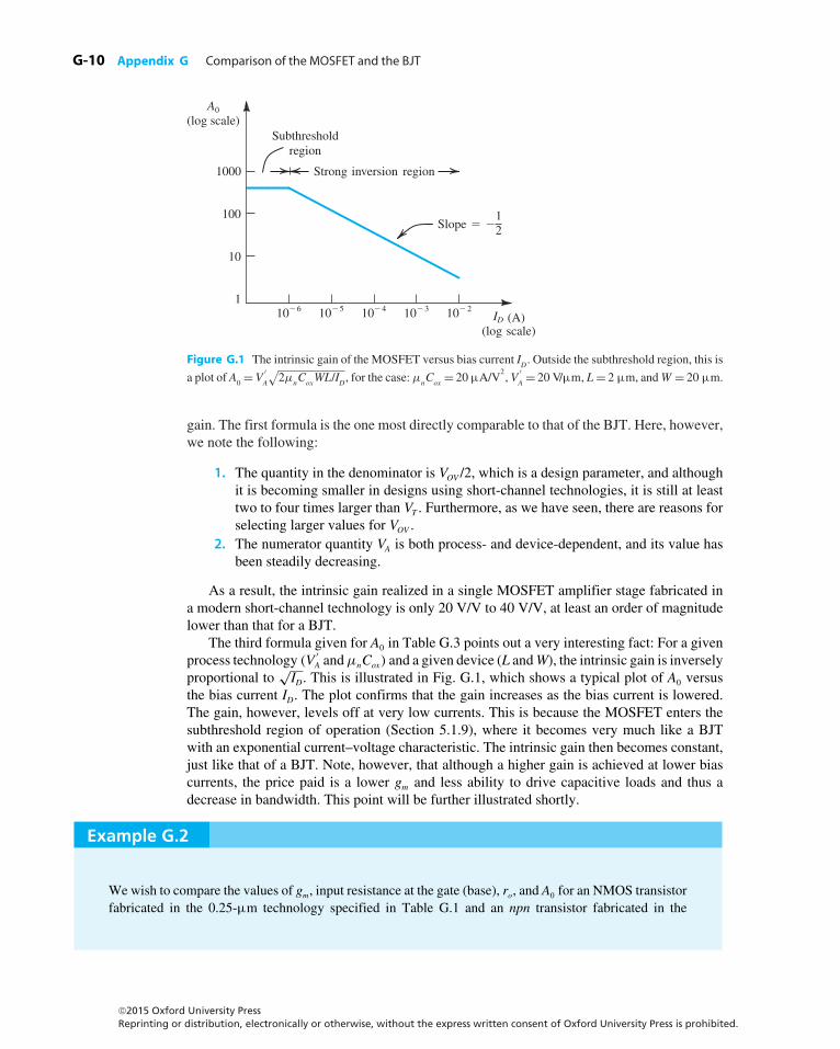
G.3.6 Intrinsic Gain
The intrinsic gain A0 of the BJT is the ratio of VA, which is solely a process parameter (5 Vto 100 V), and VT , which is a physical parameter (0.025 V at room temperature). Thus A0 ofa BJT is independent of the device junction area and of the operating current, and its valueranges from 200 V/V to 5000 V/V. The situation in the MOSFET is very different: TableG.3 provides three different (but equivalent) formulas for expressing the MOSFET’s intrinsic
©2015 Oxford University PressReprinting or distribution, electronically or otherwise, without the express written consent of Oxford University Press is prohibited.
G-10 Appendix G Comparison of the MOSFET and the BJT
A0
(log scale)
1000
100
10
110� 6 10� 5 10� 4 10� 3 10� 2
Slope � �12
Strong inversion region
Subthresholdregion
(A)ID
(log scale)
Figure G.1 The intrinsic gain of the MOSFET versus bias current ID. Outside the subthreshold region, this is
a plot of A0 =V′A
√2μnCoxWL/ID, for the case:μnCox = 20μA/V
2, V
′A = 20 V/μm, L= 2 μm, andW = 20 μm.
gain. The first formula is the one most directly comparable to that of the BJT. Here, however,we note the following:
1. The quantity in the denominator is VOV /2, which is a design parameter, and althoughit is becoming smaller in designs using short-channel technologies, it is still at leasttwo to four times larger than VT . Furthermore, as we have seen, there are reasons forselecting larger values for VOV .
2. The numerator quantity VA is both process- and device-dependent, and its value hasbeen steadily decreasing.
As a result, the intrinsic gain realized in a single MOSFET amplifier stage fabricated ina modern short-channel technology is only 20 V/V to 40 V/V, at least an order of magnitudelower than that for a BJT.
The third formula given for A0 in Table G.3 points out a very interesting fact: For a givenprocess technology (V ′
A andμnCox) and a given device (L andW), the intrinsic gain is inverselyproportional to
√ID. This is illustrated in Fig. G.1, which shows a typical plot of A0 versus
the bias current ID. The plot confirms that the gain increases as the bias current is lowered.The gain, however, levels off at very low currents. This is because the MOSFET enters thesubthreshold region of operation (Section 5.1.9), where it becomes very much like a BJTwith an exponential current–voltage characteristic. The intrinsic gain then becomes constant,just like that of a BJT. Note, however, that although a higher gain is achieved at lower biascurrents, the price paid is a lower gm and less ability to drive capacitive loads and thus adecrease in bandwidth. This point will be further illustrated shortly.
Example G.2
Wewish to compare the values of gm, input resistance at the gate (base), ro, and A0 for an NMOS transistorfabricated in the 0.25-μm technology specified in Table G.1 and an npn transistor fabricated in the
©2015 Oxford University PressReprinting or distribution, electronically or otherwise, without the express written consent of Oxford University Press is prohibited.

G.3 Comparison of Important Characteristics G-11
Example G.2 continued
low-voltage technology specified in Table G.2. Assume both devices are operating at a drain (collector)current of 100 μA. For the MOSFET, let L = 0.4 μm and W = 4 μm, and specify the required VOV .
Solution
For the NMOS transistor,
ID = 1
2
(μnCox
)(WL
)V 2OV
100 = 1
2× 267× 4
0.4×V 2
OV
Thus,
VOV = 0.27 V
gm =√2(μnCox
)(WL
)ID
= √2× 267× 10× 100 = 0.73 mA/V
Rin = ∞
ro = V ′AL
ID= 5× 0.4
0.1= 20 k�
A0 = gmro = 0.73× 20 = 14.6 V/V
For the npn transistor,
gm = ICVT
= 0.1 mA
0.025 V= 4 mA/V
Rin = rπ = β0/gm = 100
4 mA/V= 25 k�
ro = VAIC
= 35
0.1 mA= 350 k�
A0 = gmro = 4× 350 = 1400 V/V
EXERCISE
G.2 For an NMOS transistor fabricated in the 0.5-μm process specified in Table G.1 with W = 5 μm andL= 0.5 μm, find the transconductance and the intrinsic gain obtained at ID = 10 μA, 100 μA, and 1 mA.Ans. 0.2 mA/V, 200 V/V; 0.6 mA/V, 62 V/V; 2 mA/V, 20 V/V
©2015 Oxford University PressReprinting or distribution, electronically or otherwise, without the express written consent of Oxford University Press is prohibited.
G-12 Appendix G Comparison of the MOSFET and the BJT
G.3.7 High-Frequency Operation
The simplified high-frequency equivalent circuits for the MOSFET and the BJT are verysimilar, and so are the formulas for determining their unity-gain frequency (also calledtransition frequency) fT . As we demonstrate in Chapter 10, fT is a measure of the intrinsicbandwidth of the transistor itself and does not take into account the effects of capacitiveloads. We address the issue of capacitive loads shortly. For the time being, note the strikingsimilarity between the approximate formulas given in Table G.3 for the value of fT of thetwo devices. In both cases fT is inversely proportional to the square of the critical dimensionof the device: the channel length for the MOSFET and the base width for the BJT. Theseformulas also clearly indicate that shorter-channel MOSFETs4 and narrower-base BJTs areinherently capable of a wider bandwidth of operation. It is also important to note that whilefor the BJT the approximate expression for fT indicates that it is entirely process determined,the corresponding expression for the MOSFET shows that fT is proportional to the overdrivevoltage VOV . Thus we have conflicting requirements on VOV : While a higher low-frequencygain is achieved by operating at a low VOV , wider bandwidth requires an increase in VOV .Therefore the selection of a value for VOV involves, among other considerations, a trade-offbetween gain and bandwidth.
For npn transistors fabricated in the modern low-voltage process, fT is in the rangeof 10 GHz to 20 GHz as compared to the 400 MHz to 600 MHz obtained with thestandard high-voltage process. In the MOS case, NMOS transistors fabricated in a modernsubmicron technology, such as the 0.18-μm process, achieve fT values in the range of 5 GHzto 15 GHz.
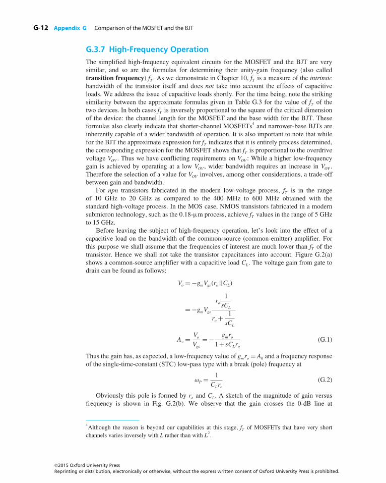
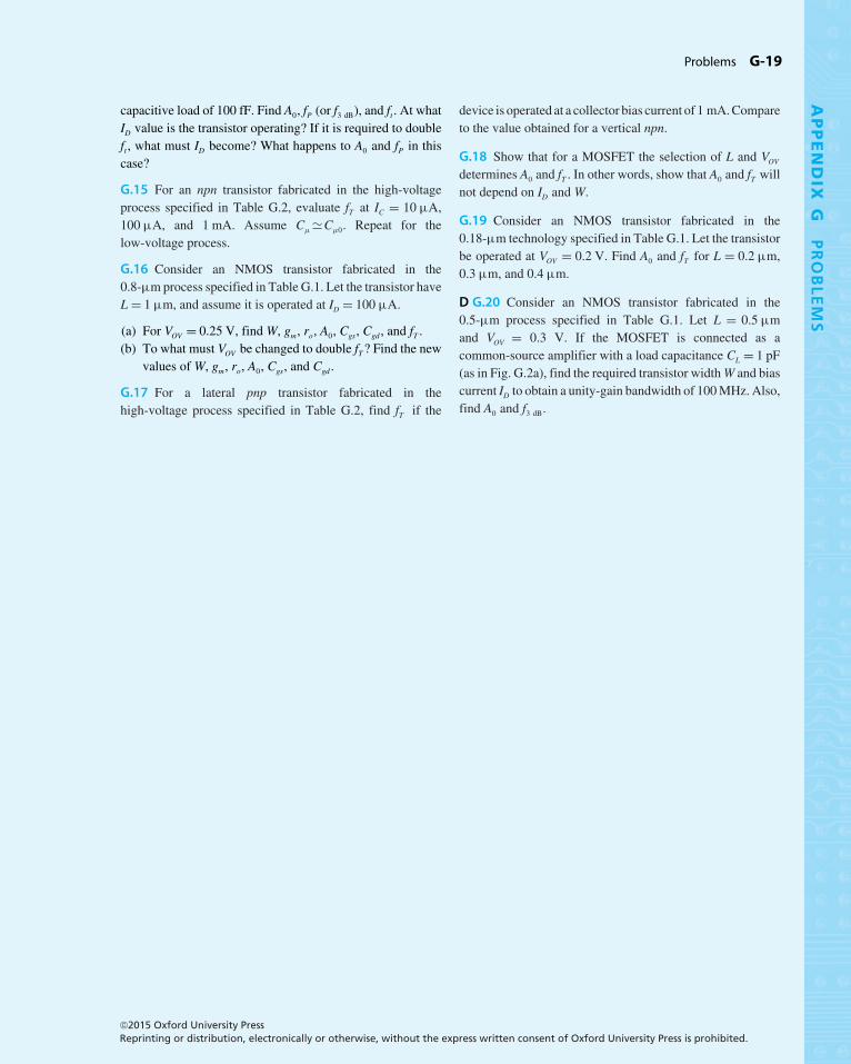
Before leaving the subject of high-frequency operation, let’s look into the effect of acapacitive load on the bandwidth of the common-source (common-emitter) amplifier. Forthis purpose we shall assume that the frequencies of interest are much lower than fT of thetransistor. Hence we shall not take the transistor capacitances into account. Figure G.2(a)shows a common-source amplifier with a capacitive load CL. The voltage gain from gate todrain can be found as follows:
Vo = −gmVgs(ro‖CL)
= −gmVgsro
1
sCL
ro + 1
sCL
Av = VoVgs
= − gmro1+ sCLro
(G.1)
Thus the gain has, as expected, a low-frequency value of gmro = A0 and a frequency responseof the single-time-constant (STC) low-pass type with a break (pole) frequency at
ωP = 1
CLro(G.2)
Obviously this pole is formed by ro and CL. A sketch of the magnitude of gain versusfrequency is shown in Fig. G.2(b). We observe that the gain crosses the 0-dB line at
4Although the reason is beyond our capabilities at this stage, fT of MOSFETs that have very shortchannels varies inversely with L rather than with L2.
©2015 Oxford University PressReprinting or distribution, electronically or otherwise, without the express written consent of Oxford University Press is prohibited.
G.3 Comparison of Important Characteristics G-13
(a)
�
�
Vo
�
�
Vgs CL
D
S
G
rogmVgs
(b)
�20 dB�decade
3 dB
0
20 log A0
frequency(log scale)
ft 2pCL
gm � fP 2pCLro
1 �
f3dB
Vo
Vgs(dB)
Figure G.2 Frequency response of a CS amplifier loaded with a capacitance CL and fed with an ideal voltagesource. It is assumed that the transistor is operating at frequencies much lower than fT , and thus the internalcapacitances are not taken into account.
frequency ωt ,
ωt = A0ωP = (gmro)1
CLroThus,
ωt = gmCL
(G.3)
That is, the unity-gain frequency or, equivalently, the gain–bandwidth product5 ωt isthe ratio of gm and CL. We thus clearly see that for a given capacitive load CL, a largergain–bandwidth product is achieved by operating the MOSFET at a higher gm. Identicalanalysis and conclusions apply to the case of the BJT. In each case, bandwidth increases asbias current is increased.
5The unity-gain frequency and the gain–bandwidth product of an amplifier are the same when thefrequency response is of the single-pole type; otherwise the two parameters may differ.
©2015 Oxford University PressReprinting or distribution, electronically or otherwise, without the express written consent of Oxford University Press is prohibited.

G-14 Appendix G Comparison of the MOSFET and the BJT
G.3.8 Design Parameters
For the BJT there are three design parameters—IC , VBE , and IS (or, equivalently, the areaof the emitter–base junction)—and the designer can select any two. However, since IC isexponentially related to VBE and is very sensitive to the value of VBE (VBE changes by only 60mV for a factor of 10 change in IC), IC is much more useful than VBE as a design parameter. Asmentioned earlier, the utility of the EBJ area as a design parameter is rather limited becauseof the narrow range over which AE can vary. It follows that for the BJT there is only oneeffective design parameter: the collector current IC . Finally, note that we have not consideredVCE to be a design parameter, since its effect on IC is only secondary. Of course, as we learnedin Chapter 7, VCE affects the output-signal swing.
For the MOSFET there are four design parameters— ID, VOV , L, andW—and the designercan select any three. For analog circuit applications the trade-off in selecting a value for L isbetween the higher speed of operation (wider amplifier bandwidth) obtained at lower valuesof L and the higher intrinsic gain obtained at larger values of L. Usually one selects an L ofabout 25% to 50% greater than Lmin.
The second design parameter is VOV . We have already made numerous remarks aboutthe effect of the value of VOV on performance. Usually, for submicron technologies, VOV isselected in the range of 0.1 V to 0.3 V.
Once values for L and VOV have been selected, the designer is left with the selection of thevalue of ID orW (or, equivalently,W/L). For a given process and for the selected values ofL andVOV , ID is proportional toW/L. It is important to note that the choice of ID or, equivalently, ofW/L has no bearing on the value of intrinsic gainA0 and the transition frequency fT . However, itaffects the value of gm and hence the gain–bandwidth product. Figure G.3 illustrates this pointby showing how the gain of a common-source amplifier operated at a constant VOV varies withID (or, equivalently,W/L). Note that while the dc gain remains unchanged, increasingW/L and,correspondingly, ID, increases the bandwidth proportionally. This, however, assumes that theload capacitance CL is not affected by the device size, an assumption that may not be entirelyjustified in some cases.
20 log A0
f(log scale)
ft 2pCLgm � f3dB 2pCLro
1 �
�Gain�(dB)
ID and WL
0
Figure G.3 Increasing ID orW/L increases the bandwidth of a MOSFET amplifier operated at a constant VOVand loaded by a constant capacitance CL .
©2015 Oxford University PressReprinting or distribution, electronically or otherwise, without the express written consent of Oxford University Press is prohibited.
G.3 Comparison of Important Characteristics G-15
Example G.3
In this example we investigate the gain and the high-frequency response of an npn transistor and an NMOStransistor. For the npn transistor, assume that it is fabricated in the low-voltage process specified in TableG.2, and assume that Cμ � Cμ0. For IC = 10 μA, 100 μA, and 1 mA, find gm, ro, A0, Cde, Cje, Cπ , Cμ, andfT . Also, for each value of IC , find the gain–bandwidth product ft of a common-emitter amplifier loadedby a 1-pF capacitance, neglecting the internal capacitances of the transistor. For the NMOS transistor,assume that it is fabricated in the 0.25-μm CMOS process with L = 0.4 μm. Let the transistor be operatedat VOV = 0.25 V. Find W/L that is required to obtain ID = 10 μA, 100 μA, and 1 mA. At each value ofID, find gm, ro, A0, Cgs, Cgd , and fT . Also, for each value of ID, determine the gain–bandwidth productfT of a common-source amplifier loaded by a 1-pF capacitance, neglecting the internal capacitances ofthe transistor.
Solution
For the npn transistor,
gm = ICVT
= IC0.025
= 40ICA/V
ro = VAIC
= 35
IC�
A0 = VAVT
= 35
0.025= 1400 V/V
Cde = τFgm = 10× 10−12 × 40IC = 0.4× 10⁻⁹IC F
Cje � 2Cje0 = 10 fF
Cπ = Cde +Cje
Cμ � Cμ0 = 5 fF
fT = gm2π(Cπ +Cμ
)ft =
gm2πCL
= gm2π × 1× 10−12
We thus obtain the following results:
ro (k )
10 μ A 100 μ A 1 mA
0.4 4
40
3500 350 35
1400 1400 1400
4 40
400
10 10 10
14 50
410
5 5 5
3.4 11.6 15.3
64 640
6400
IC gm (mA/V) A0 (V/V) Cde (f F) Cje (f F) Cπ (f F) Cμ (f F) fT (GHz) ft (MHz)
©2015 Oxford University PressReprinting or distribution, electronically or otherwise, without the express written consent of Oxford University Press is prohibited.
G-16 Appendix G Comparison of the MOSFET and the BJT
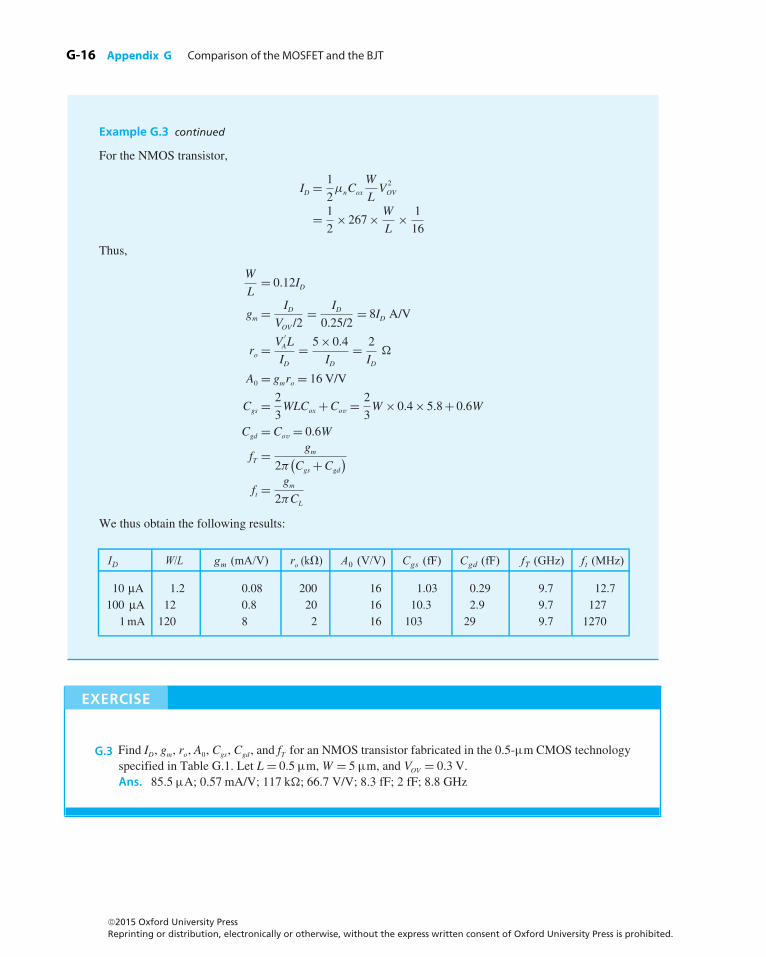
Example G.3 continued
For the NMOS transistor,
ID = 1
2μnCox
W
LV 2OV
= 1
2× 267× W
L× 1
16
Thus,
W
L= 0.12ID
gm = IDVOV /2
= ID0.25/2
= 8ID A/V
ro = V ′AL
ID= 5× 0.4
ID= 2
ID�
A0 = gmro = 16 V/V
Cgs =2
3WLCox +Cov = 2
3W × 0.4× 5.8+ 0.6W
Cgd = Cov = 0.6W
fT = gm2π(Cgs +Cgd
)ft =
gm2πCL
We thus obtain the following results:
W/L ro (k )
10 μ A 100 μ A
1 mA
1.2 12
120
0.08 0.8 8
200 20
2
16 16 16
1.03 10.3
103
0.29 2.9
29
9.7 9.7 9.7
12.7 127
1270
ID gm (mA/V) A0 (V/V) Cgs (fF) Cgd (fF) fT (GHz) ft (MHz)
EXERCISE
G.3 Find ID, gm, ro, A0, Cgs, Cgd , and fT for an NMOS transistor fabricated in the 0.5-μm CMOS technologyspecified in Table G.1. Let L = 0.5 μm, W = 5 μm, and VOV = 0.3 V.Ans. 85.5 μA; 0.57 mA/V; 117 k�; 66.7 V/V; 8.3 fF; 2 fF; 8.8 GHz
©2015 Oxford University PressReprinting or distribution, electronically or otherwise, without the express written consent of Oxford University Press is prohibited.

G.5 Validity of the Square-Law MOSFET Model G-17
G.4 Combining MOS and BipolarTransistors—BiCMOS Circuits
From the discussion above it should be evident that the BJT has the advantage over theMOSFET of a much higher transconductance (gm) at the same value of dc bias current. Thus,in addition to realizing higher voltage gains per amplifier stage, bipolar transistor amplifiershave superior high-frequency performance compared to their MOS counterparts.
On the other hand, the practically infinite input resistance at the gate of a MOSFETmakesit possible to design amplifiers with extremely high input resistances and an almost zero inputbias current. Also, as mentioned earlier, the MOSFET provides an excellent implementationof a switch, a fact that has made CMOS technology capable of realizing a host of analogcircuit functions that are not possible with bipolar transistors.
It can thus be seen that each of the two transistor types has its own distinct and uniqueadvantages: Bipolar technology has been extremely useful in the design of very-high-qualitygeneral-purpose circuit building blocks, such as op amps. On the other hand, CMOS, with itsvery high packing density and its suitability for both digital and analog circuits, has become thetechnology of choice for the implementation of very-large-scale integrated circuits. Neverthe-less, the performance of CMOS circuits can be improved if the designer has available (on thesame chip) bipolar transistors that can be employed in functions that require their high gm andexcellent current-driving capability. A technology that allows the fabrication of high-qualitybipolar transistors on the same chip as CMOS circuits is aptly calledBiCMOS. At appropriatelocations throughout this book we present interesting and useful BiCMOS circuit blocks.
G.5 Validity of the Square-Law MOSFET Model
We conclude this appendix with a comment on the validity of the simple square-law modelwe have been using to describe the operation of the MOS transistor. While this simplemodel works well for devices with relatively long channels (>1μm), it does not provide anaccurate representation of the operation of short-channel devices. This is because a numberof physical phenomena come into play in these submicron devices, resulting in what arecalled short-channel effects. Although a detailed study of short-channel effects is beyondthe scope of this book, it should be mentioned that MOSFET models have been developedthat take these effects into account. However, they are understandably quite complex anddo not lend themselves to hand analysis of the type needed to develop insight into circuitoperation. Rather, these models are suitable for computer simulation and are indeed usedin SPICE (Appendix B). For quick, manual analysis, however, we will continue to use thesquare-law model, which is the basis for the comparison of Table G.3.
©2015 Oxford University PressReprinting or distribution, electronically or otherwise, without the express written consent of Oxford University Press is prohibited.
PROBLEMS
G.1 Find the range of ID obtained in a particular NMOStransistor as its overdrive voltage is increased from 0.15 Vto 0.4 V. If the same range is required in IC of a BJT, what isthe corresponding change in VBE?
G.2 What range of IC is obtained in an npn transistor as aresult of changing the area of the emitter–base junction by afactor of 10 while keeping VBE constant? If IC is to be keptconstant, by what amount must VBE change?
G.3 For each of the CMOS technologies specified inTable G.1, find the
∣∣VOV ∣∣ and hence the∣∣VGS∣∣ required to
operate a device with a W/L of 10 at a drain current ID =100 μA. Ignore channel-length modulation.
G.4 Consider NMOS and PMOS devices fabricated in the0.25-μm process specified in Table G.1. If both devices areto operate at
∣∣VOV ∣∣= 0.25 V and ID = 100 μA,whatmust theirW/L ratios be?
G.5 Consider NMOS and PMOS transistors fabricated inthe 0.25-μm process specified in Table G.1. If the twodevices are to be operated at equal drain currents, what mustthe ratio of (W/L)p to (W/L)n be to achieve equal valuesof gm?
G.6 An NMOS transistor fabricated in the 0.18-μm CMOSprocess specified in Table G.1 is operated at VOV = 0.2 V.Find the required W/L and ID to obtain a gm of 10 mA/V. Atwhat value of IC must an npn transistor be operated to achievethis value of gm?
G.7 For each of the CMOS process technologies specified inTable G.1, find the gm of an NMOS and a PMOS transistorwith W/L= 10 operated at ID = 100 μA.
G.8 An NMOS transistor operated with an overdrive voltageof 0.25 V is required to have a gm equal to that of an npntransistor operated at IC = 0.1 mA. What must ID be? Whatvalue of gm is realized?
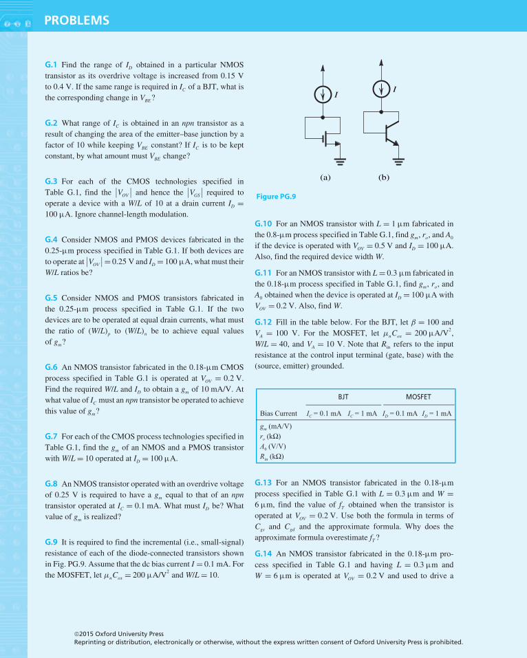
G.9 It is required to find the incremental (i.e., small-signal)resistance of each of the diode-connected transistors shownin Fig. PG.9. Assume that the dc bias current I = 0.1 mA. Forthe MOSFET, let μnCox = 200 μA/V2 and W/L= 10.
(a)
I
(b)
I
Figure PG.9
G.10 For an NMOS transistor with L = 1 μm fabricated inthe 0.8-μm process specified in Table G.1, find gm, ro, and A0
if the device is operated with VOV = 0.5 V and ID = 100 μA.Also, find the required device widthW.
G.11 For an NMOS transistor with L= 0.3 μm fabricated inthe 0.18-μm process specified in Table G.1, find gm, ro, andA0 obtained when the device is operated at ID = 100 μA withVOV = 0.2 V. Also, findW.
G.12 Fill in the table below. For the BJT, let β = 100 andVA = 100 V. For the MOSFET, let μnCox = 200 μA/V2,W/L = 40, and VA = 10 V. Note that Rin refers to the inputresistance at the control input terminal (gate, base) with the(source, emitter) grounded.
BJT MOSFET
Bias Current IC = 0.1 mA IC = 1 mA ID = 0.1 mA ID = 1 mA
gm (mA/V)
ro (kΩ )A0 (V/V)
Rin (kΩ )
G.13 For an NMOS transistor fabricated in the 0.18-μmprocess specified in Table G.1 with L = 0.3 μm and W =6 μm, find the value of fT obtained when the transistor isoperated at VOV = 0.2 V. Use both the formula in terms ofCgs and Cgd and the approximate formula. Why does theapproximate formula overestimate fT?
G.14 An NMOS transistor fabricated in the 0.18-μm pro-cess specified in Table G.1 and having L = 0.3 μm andW = 6 μm is operated at VOV = 0.2 V and used to drive a
©2015 Oxford University PressReprinting or distribution, electronically or otherwise, without the express written consent of Oxford University Press is prohibited.
AP
PE
ND
IXG
PR
OB
LEM
S
Problems G-19
capacitive load of 100 fF. Find A0, fP (or f3 dB), and ft . At whatID value is the transistor operating? If it is required to doubleft , what must ID become? What happens to A0 and fP in thiscase?
G.15 For an npn transistor fabricated in the high-voltageprocess specified in Table G.2, evaluate fT at IC = 10 μA,100 μA, and 1 mA. Assume Cμ �Cμ0. Repeat for thelow-voltage process.
G.16 Consider an NMOS transistor fabricated in the0.8-μmprocess specified in Table G.1. Let the transistor haveL = 1 μm, and assume it is operated at ID = 100 μA.
(a) For VOV = 0.25 V, findW, gm, ro, A0, Cgs, Cgd , and fT .(b) To what must VOV be changed to double fT? Find the new
values ofW, gm, ro, A0, Cgs, and Cgd .
G.17 For a lateral pnp transistor fabricated in thehigh-voltage process specified in Table G.2, find fT if the
device is operated at a collector bias current of 1 mA.Compareto the value obtained for a vertical npn.
G.18 Show that for a MOSFET the selection of L and VOVdetermines A0 and fT . In other words, show that A0 and fT willnot depend on ID and W.
G.19 Consider an NMOS transistor fabricated in the0.18-μm technology specified in Table G.1. Let the transistorbe operated at VOV = 0.2 V. Find A0 and fT for L = 0.2 μm,0.3 μm, and 0.4 μm.
D G.20 Consider an NMOS transistor fabricated in the0.5-μm process specified in Table G.1. Let L = 0.5 μmand VOV = 0.3 V. If the MOSFET is connected as acommon-source amplifier with a load capacitance CL = 1 pF(as in Fig. G.2a), find the required transistor widthW and biascurrent ID to obtain a unity-gain bandwidth of 100MHz. Also,find A0 and f3 dB.
©2015 Oxford University PressReprinting or distribution, electronically or otherwise, without the express written consent of Oxford University Press is prohibited.


![Practical setup of power electronics lab power semicondutor devices [ scr, mosfet, igbt, gto, traic,bjt ]](https://static.fdocuments.net/doc/165x107/53f511a78d7f7246588b45e2/practical-setup-of-power-electronics-lab-power-semicondutor-devices-scr-mosfet-igbt-gto-traicbjt-.jpg)


