Comparative Evaluation of 800V DC-Link Three-Phase Two ...
7
© 2020 IEEE Proceedings of the 23rd International Conference on Electrical Machines and Systems (ICEMS2020), Hamamatsu, Japan, November 24-27, 2020 Comparative Evaluation of 800V DC-Link Three-Phase Two/Three-Level SiC Inverter Concepts for Next-Generation Variable Speed Drives D. Cittanti, M. Guacci, S. Miric, R. Bojoi, J. W. Kolar Personal use of this material is permitted. Permission from IEEE must be obtained for all other uses, in any current or future media, including reprinting/republishing this material for advertising or promotional purposes, creating new collective works, for resale or redistribution to servers or lists, or reuse of any copyrighted component of this work in other works.
Transcript of Comparative Evaluation of 800V DC-Link Three-Phase Two ...

© 2020 IEEE
Proceedings of the 23rd International Conference on Electrical Machines and Systems (ICEMS2020), Hamamatsu, Japan, November 24-27, 2020
Comparative Evaluation of 800V DC-Link Three-Phase Two/Three-Level SiC Inverter Concepts for Next-Generation Variable Speed Drives
D. Cittanti,M. Guacci,S. Miric,R. Bojoi,J. W. Kolar
Personal use of this material is permitted. Permission from IEEE must be obtained for all other uses, in any current or future media, including reprinting/republishing this material for advertising or promotional purposes, creating new collective works, for resale or redistribution to servers or lists, or reuse of any copyrighted component of this work in other works.

Comparative Evaluation of 800 V DC-LinkThree-Phase Two/Three-Level SiC Inverter Concepts
for Next-Generation Variable Speed DrivesDavide Cittanti§, Mattia Guacci∗, Spasoje Miric∗, Radu Bojoi§ and Johann W. Kolar∗
§Department of Energy “G. Ferraris”, Politecnico di Torino, Italy∗Power Electronic Systems Laboratory, ETH Zurich, Switzerland
Abstract—The adoption of wide band-gap (WBG) semiconductors isgaining momentum, particularly in industries where high efficiency and/orextreme power density are major concerns, e.g. electric transportation andaerospace. In order to fully leverage the advantages of WBG devices, iden-tifying the converter topologies best exploiting their superior performanceis of utmost importance. Hence, this paper analyzes and compares 2-leveland 3-level SiC-based three-phase inverters for next-generation variablespeed drives. Full sine-wave filtering at the converter output is assumedto counteract the negative effects of the fast switching transitions of WBGdevices on the driven machine. The stresses on the active and passivecomponents, i.e. semiconductor losses, output inductor flux ripple and DC-link capacitor RMS current, are calculated by analytical and/or numericalmeans. Moreover, the optimal semiconductor chip area, the power lossesand the efficiency of each converter topology are investigated as functionsof the switching frequency, providing a theoretical performance limit foreach solution. Finally, a multi-objective optimization targeting an 800V7.5kW system is carried out. The results are in good agreement with thetheoretical performance analysis and provide an overview of the achievableefficiency vs. power density trade-off for all the considered topologies.
Index Terms—Variable Speed Drives, 2-Level Inverters, 3-Level Invert-ers, Wide Band-Gap Semiconductors, Semiconductor Chip Area, Multi-Objective Optimization.
I. INTRODUCTION
Modern wide band-gap (WBG) semiconductors simultaneously en-able efficiency and power density improvements in advanced powerconverters, as they offer unprecedented performance, leveraging ontheir higher switching speeds. However, fast voltage variations duringswitching transitions can have harmful effects in variable speed drives(VSDs), such as partial discharges in the insulating materials, i.e.motor insulation aging, voltage reflections in motor cables and bearingcurrents [1]. These effects can be avoided either by reducing theswitching speed, or by full sine-wave filtering the inverter outputvoltage. While the former strategy increases the switching losses tounacceptable levels inhibiting the core advantage of WBG devices, thelatter shifts the high-frequency stresses from the motor to the outputfilter, generally enabling an overall efficiency increase [2]. Additionally,the higher switching frequencies introduced by WBG devices limitthe impact of the filter on the converter power density, and higherefficiency-to-volume figures can be achieved with respect to state-of-the-art Si-based solutions [3]. For the stated reasons, a VSD includinga full sine-wave filter is considered throughout this work.
The most adopted converter topology for industrial VSDs is thethree-phase (3-Φ) 2-level (2-L) inverter [1], mainly due to its simplicityand well understood operation. Nevertheless, when high DC-link volt-ages are required (e.g. 800 V) the performance of this converter rapidlyworsens [4], since devices with high voltage ratings are required andlarge high-frequency voltage harmonics are applied to the output filter,due to the 2-L nature of the switched voltage waveform. Three-level(3-L) inverter topologies represent excellent candidates to address theoutput filter size reduction, taking advantage of the increased numberof output voltage levels [4], [5]. Moreover, employing devices withreduced voltage ratings, they ensure superior performance [6]. Eventhough the performance characteristics of 2-L and 3-L converters have
(a) (b) (c) (d) (e) (f)
Tp,l
Tp,h
Tn,l
Tn,h
p
n
m
Tp
Tn
p
n
Tp,l
Tp,h
Tn,h
Tn,l
p
n
Tp,l
Tp,h
Dp,m
Tn,l
Tn,hDn,m
p
n
m
Tp,l
Tp,h
Tp,m
Tn,l
Tn,hTn,m
p
n
m
Tx,h
Tx,l
Tp,l
Tp,h
Tn,h
Tn,l
p
n
m
Fig. 1: Schematic of a single-phase bridge-leg of the (a) 2-level converter (2LC), (b) 3-level T-type converter (3LTTC), (c) 3-level neutral point clamped converter(3LNPCC), (d) 3-level active neutral point clamped converter (3LANPCC), (e) 3-level flying capacitor converter (3LFCC) and (f) 3-level sparse neutral pointclamped converter (3LSNPCC). The 3LSNPCC bridge-leg includes the 3-L switching matrix and one 2-L inverter bridge-leg [9].
already been investigated in literature [4], [5], [7]–[9], a comprehensivecomparison between topologies taking into account the differential-mode (DM) and common-mode (CM) sine-wave filter stresses, theconduction/switching losses in the devices and the loss-optimal semi-conductor chip area has yet to be addressed.
Accordingly, this paper conducts a comparative evaluation of themost suitable converter topologies for 3-Φ 800 V 7.5 kW SiC-basedVSDs. This analysis considers the conventional 2-L converter (2LC)and the most widespread 3-L topologies (see Fig. 1), which includethe T-Type converter (3LTTC), the Neutral Point Clamped converter(3LNPCC), the Active NPC converter (3LANPCC) and the Flying Ca-pacitor converter (3LFCC). In addition, the 3-L Sparse NPC converter(3LSNPCC), introduced in [10] and analyzed in [9], [11], is considered.
The major component stresses for each topology, such as the DMand CM inductor flux ripples, the DC-link capacitor RMS current andthe semiconductor losses, are calculated in Section II. In Section III, achip area optimization procedure is proposed and applied to an 800 V,7.5 kW inverter adopting SiC MOSFETs (and SiC diodes, for the3LNPCC). The results, expressed in terms of required filtering effortfor a given efficiency target, are discussed. In Section IV, the efficiencyvs. power density performance limits of each converter are identified bymeans of a multi-objective optimization procedure. Finally, a summaryof the main results of this work is provided in Section V.
II. COMPONENT STRESSES
The current and/or voltage stresses of the passive and active sys-tem components directly affect the converter design. In this section,analytical expressions are derived for all major component stresses.
A. DM and CM InductorsThe AC sine-wave filter topology illustrated in Fig. 2, composed of
a DM and a CM filter stage, is considered herein. The most significantparameters for the design and operation of the DM and CM filterinductors are the maximum peak-to-peak and RMS flux ripple values,since the former determines the magnetic core saturation, while thelatter translates in inductor winding and core losses. As the RMS fluxripple provides more information on the ripple over the complete 3-Φoutput period, this is selected as the representative performance index.Assuming sufficiently large DM and CM filter capacitances (CDM,CCM), the RMS flux ripple in the filter inductors can be analyticallyderived as in [9] with the knowledge of the DM and CM inverter voltagewaveforms, which depend on the converter topology and the adoptedmodulation strategy. Sinusoidal third-harmonic injection modulation(THIPWM) [12] is considered for the 2LC, 3LTTC, 3LNPCC, 3LAN-PCC (PWM-1 in [7]) and 3LFCC (as in [13]), while asymmetricalswitching sequence O [9] is assumed for the 3LSNPCC (i.e. showingthe best switching loss vs. flux-ripple trade-off). Due to the complexityof the analytically derived expressions, they are not reported herein.Nevertheless, the DM, CM and total RMS flux ripples, respectively∆ΨDM,RMS, ∆ΨCM,RMS and ∆ΨRMS =
√∆Ψ2
DM,RMS + ∆Ψ2CM,RMS, are
illustrated in normalized form (i.e. ∆Ψn = Vdc/fsw, where fsw is theconverter switching frequency) in Fig. 3.

ia
ib
ic
a
b
c
m
LDM LCM
CDM
CCM
vDM,a
vDM,b
vDM,c
vCM
Fig. 2: Equivalent circuit of a 3-Φ inverter with the considered full sine-wavefilter. The DM and CM voltages are represented by ideal switched voltagesources. Point m in the 2LC and the 3LFCC is obtained by splitting the DC-link.
(a) (b) (c)
2LC 3LTTC 3LNPCC 3LANPCC 3LFCC 3LSNPCC
Fig. 3: Normalized RMS (a) DM flux ripple ∆ΨDM,RMS/∆Ψn, (b) CM fluxripple ∆ΨCM,RMS/∆Ψn and (c) total flux ripple ∆ΨRMS/∆Ψn, as functionsof the modulation index M . The curves related to the 3LTTC, 3LNPCC and3LANPCC are superimposed, since these converters yield the same outputvoltage waveform.
B. DC-Link CapacitorsNeglecting the phase current ripple, the RMS current flowing into the
DC-link capacitors in balanced conditions is the same for all convertersand is independent on the modulation strategy [9], [14]:
ICdc ,RMS = I
√M
[√3
4π+ cos2 ϕ
(√3
π− 9M
16
)], (1)
where I is the phase current fundamental amplitude and ϕ is the loadpower factor angle. Nevertheless, the DC-link peak-to-peak voltageripple generally depends on the modulation strategy itself. This effectis taken into account for the DC-link capacitor sizing in the multi-objective optimization procedure described in Section IV.
C. Semiconductor DevicesConduction Losses
If MOSFETs are considered, the conduction losses have a purelyresistive behavior and are proportional to the square of the conductedRMS current IRMS. However, to estimate the conduction losses in thediodes of the 3LNPCC, the average current IAVG is also needed. Hence,the simplified conduction loss model adopted in this work is
Pcond = Vth IAVG +RI2RMS, (2)
where Vth is the diode voltage threshold (Vth = 0 for MOSFETs) andR is the on-state (differential) resistance.
Neglecting the phase current ripple, it can be demonstrated that theRMS value of the current flowing through all MOSFETs in the 2LC andthe 3LFCC is independent on the modulation strategy and equals I/2.Nevertheless, the remaining 3-L converters yield more complicatedexpressions. If THIPWM is considered for the 3LTTC, 3LNPCC and3LANPCC,
Ip,RMS = In,RMS = I
√M
(37
90π+
7
30πcos2 ϕ
), (3)
Im,RMS = I
√1
2−M
(37
45π+
7
15πcos2 ϕ
), (4)
Im,AVG =IM
2
[cosϕ
(2|ϕ|π
+cosϕ sin|ϕ|
3π−1
)− 7 sin|ϕ|
3π+
4
π
], (5)
TABLE I: Average and RMS current stress expressions for the semiconductordevices of all the considered converter topologies.
Topology Device IAVG IRMS
2LC Tp, Tn − I/2
3LTTCTp,h, Tn,l − Ip,RMS = In,RMS
Tp,l, Tn,h − Im,RMS
3LNPCCTp,h, Tn,l − Ip,RMS = In,RMS
Tp,l, Tn,h − I/2
Dp,m, Dn,m Im,AVG/2 Im,RMS/√
2
3LANPCCTp,h, Tn,l − Ip,RMS = In,RMS
Tp,l, Tn,h − I/2
Tp,m, Tn,m − Im,RMS/√
2
3LFCCTp,h, Tn,l, − I/2Tp,l, Tn,h
3LSNPCCTx,h, Tx,l − I/2
Tp,h, Tn,l − ITp,h ,RMS
Tp,l, Tn,h − ITp,l ,RMS
where subscripts p, n and m refer to the currents flowing in the positive,negative and middle DC-link rails, respectively, can be convenientlyderived. In fact, (3), (4) and (5) are sufficient to completely identifythe current stresses in all semiconductor devices, as reported in Ta-ble I. Finally, the RMS current expressions for the transistors of the3LSNPCC are ITx,h ,RMS = ITx,l ,RMS = I/2 for the 2-L inverter devicesand
ITp,h ,RMS = ITn,l ,RMS = I
√√3
4πM(4 cos2 ϕ+ 1), (6)
ITp,l ,RMS = ITn,h ,RMS =I
√1
2−√
3
8π
[6M+cos(2ϕ) (M−3)
]Area I
I
√1
2−√
3
4π
[3M−cos(2ϕ) (
√3π−3−2M)
]Area II
, (7)
for the 3-L switching matrix devices, where area I and area II aredefined in [11].
Switching LossesThe switching losses of a generic MOSFET half-bridge can be
expressed as [15]
Esw = Qoss(Vsw)Vsw +Qrr(isw)Vsw +1
2
V 2sw
dv/dtisw +
1
2
Vswdi/dt
i2sw, (8)
where Vsw and isw are the switched voltage and current, respectively,Qoss is the charge stored in the semiconductor device non-linear outputcapacitance and Qrr is the reverse-recovery charge of the MOSFETbody-diode. The last two terms of (8) represent the v-i overlap lossesand depend on the voltage and current time derivatives during theoverlap time. Soft-switching transitions, i.e. with isw < 0, are typicallyconsidered lossless.
Assuming infinitely fast transitions, the v-i overlap loss contributionscan be neglected and the Qrr becomes equal to the forward-biasinjected charge [16], i.e. Qrr ≈ τ isw, where τ is the charge carrierrecombination lifetime.This approximation results in a linear switchingloss model with respect to the switched current, obtaining
Esw(isw) ≈ Qoss(Vsw)Vsw + τ Vsw isw = k0 + k1 isw, (9)
which represents a theoretical lower limit for the switching losses andis in a first approximation met in practice for semiconductor deviceswith high switching performance [6].
Equations (8) and (9) quantify the hard switching losses generatedin a conventional half-bridge with identical high-side and low-sidesemiconductor devices. However, these expressions can be extendedto other bridge-leg topologies by analyzing the capacitive and reverse-recovery charges involved in each commutation process, depending onthe topology being considered and on the different devices involved inthe transition. To facilitate this, the equivalent circuit of a 3-L bridge-leg illustrated in Fig. 4 is considered. In general, a total of four differentswitching events can occur, depending on the direction of the switch-

(a) (b)
(c) (d)
Tl
Th
i < 0
Coss,h
Coss,x
Coss,l
Vdc2 Tl
Th Coss,h
Coss,x
Coss,l
Vdc2
Tl
Th Coss,h
Coss,x
Coss,l
Vdc2
Vdc2
Tl
Th Coss,h
Coss,x
Coss,l
Vdc2
Vdc2
i < 0
i > 0
i > 0
Fig. 4: Equivalent circuits of a generic 3-L bridge-leg involved in the fourpossible hard-switching events: the current paths before and after the transitionare highlighted in pink and blue, respectively. Coss,x represents the outputcapacitance of a generic device subject to voltage variation but not directlyinvolved in the commutation.
Vdc/2 Vdc
Qos
s
Voss (V)
Ea
Qoss(Vdc)
QossVdc2
Eb
Ec
Ed
Fig. 5: Graphical representation of the capacitive energy components Ea, Eb, Ecand Ed of a generic semiconductor device in a 3-L inverter with Vdc = 800 V.
node current i and the magnitude of the offset voltage applied to theswitch-node capacitance Coss,x. Transistors Th and Tl represent thetwo switches directly involved in the commutation process, while Coss,xrepresents the output capacitance of a generic device which is subject tothe voltage variation. All four switching events (a), (b), (c) and (d) areanalyzed under the hypothesis of instantaneous transitions (i.e. no v-ioverlap losses), exploiting the energy balance method reported in [17].For reasons of conciseness, the following energy terms are defined:
Ea = Eoss(Vdc/2), (10)
Eb = Qoss(Vdc/2)Vdc
2− Eoss(Vdc/2), (11)
Ec = [Eoss(Vdc)−Eoss(Vdc/2)]− [Qoss(Vdc)−Qoss(Vdc/2)]Vdc
2, (12)
Ed = [Qoss(Vdc)−Qoss(Vdc/2)]Vdc − [Eoss(Vdc)−Eoss(Vdc/2)], (13)
where Qoss and Eoss refer respectively to the charge and the energystored in the generic capacitance Coss. These expressions are graphi-cally illustrated in Fig. 5 for Vdc = 800 V. Leveraging (10)-(13), thecapacitive losses for the four switching events are
Eloss,(a) = Eb,h + Ea,l + Ea,x, (14)
Eloss,(b) = Ea,h + Eb,l + Eb,x, (15)
Eloss,(c) = Eb,h + Ea,l + Ec,x, (16)
Eloss,(d) = Ea,h + Eb,l + Ed,x, (17)
where subscripts h, l and x refer to Coss,h, Coss,l and Coss,x, respectively.For instance, the hard switching commutation in (a) and (c) is the same,however a Vdc/2 output DC-bias is present in the latter case. When Thturns off, i transitions from the MOSFET channel to its body diode,until Tl is turned on. Once this occurs, the capacitive energy stored inCoss,l is dissipated (Ea,l) and part of the energy provided by the DC-link to charge Coss,h is lost in the circuit resistances (Eb,h). The outputcapacitance Coss,x is practically in parallel with Tl, however it is subject
TABLE II: Overview of the capacitive losses for all the considered topologies.Where possible, the symmetry between upper and lower half of the bridge-legis exploited (i.e. the results are the same and thus not reported). Moreover, thesemiconductor devices subject to equal current and switching stresses duringa 3-Φ output period are considered to be equal, e.g. Tp = Tn for the 2LC,Tp,h =Tp,l =Tn,h =Tn,l for the 3LFCC, etc. (cf. Table I). The hard-switchingevents are defined by the direction of the current flowing out of the equivalentswitch-node involved in the transition (i.e. i, cf. Fig. 4).
Topology Transition Capacitive Losses
2LCTp ← Tn (i>0)
Qoss,Tp (Vdc)Vdc
Tp → Tn (i<0)
3LTTCTp,h ← Tp,l (i>0) Ea,Tp,h +Eb,Tp,l +Ed,Tn,l
Tp,h → Tp,l (i<0) Eb,Tp,h +Ea,Tp,l +Ec,Tn,l
3LNPCCTp,h ← Tn,h (i>0) Ea,Tp,h +Eb,Tn,h +Eb,Dp,m
Tp,h → Tn,h (i<0) Eb,Tp,h +Ea,Tn,h +Ea,Dp,m
3LANPCCTp,h ← Tp,m (i>0) Ea,Tp,h +Eb,Tn,h +Eb,Tp,m
Tp,h → Tp,m (i<0) Eb,Tp,h +Ea,Tn,h +Ea,Tp,m
3LFCC
Tp,h ← Tn,l (i>0) Qoss,Tp,h (Vdc/2)Vdc/2Tp,h → Tn,l (i<0)
Tp,l ← Tn,h (i>0)
Tp,l → Tn,h (i<0)
3LSNPCC
Tx,h ← Tx,l (i>0)Qoss,Tx,h (Vsw)Vsw*
Tx,h → Tx,l (i<0)
Tp,h ← Tp,l (i>0, Tn,h on) Ea,Tp,h +Eb,Tp,l +3Eb,Tx,h
Tp,h → Tp,l (i<0, Tn,h on) Eb,Tp,h +Ea,Tp,l +3Ea,Tx,h
Tp,h ← Tp,l (i>0, Tn,l on) Ea,Tp,h +Eb,Tp,l +3Ed,Tx,h
Tp,h → Tp,l (i<0, Tn,l on) Eb,Tp,h +Ea,Tp,l +3Ec,Tx,h
*Vsw = 0, Vdc/2, Vdc depending on the 3-L switching matrix state [9].
TABLE III: Nominal operating conditions of the considered VSD system.
Parameter Description Value
Vdc DC-link voltage 800 V
M modulation index 0.85
V peak output phase voltage 340 V
I peak output phase current 14.7 A
cosϕ power factor 1
P output power 7.5 kW
f output frequency 0 . . . 300 Hz
to different voltage transitions in the two situations, dissipating Ea,x in(a) (Vdc/2→ 0) and Ec,x in (c) (Vdc → Vdc/2). Therefore, applying theseconsiderations to each topology and analyzing all different switchingtransition, the results reported in Table II are obtained.
III. OPTIMAL CHIP AREA
In this section, the loss-optimal semiconductor chip area for eachtopology is calculated, in order to identify a theoretical upper limit tothe efficiency performance of each solution. The component losses arecalculated based on simplified analytical models given in Section II.This analysis is applied to an 800 V 7.5 kW VSD, assuming thenominal operating conditions reported in Table III and market availablesemiconductor devices.
A. Semiconductor Statistical Analysis
First, the relevant performance characteristics of the consideredsemiconductor devices must be identified. For the sake of the presentanalysis, the 3rd generation SiC MOSFETs and the 5th generation SiCdiodes from Wolfspeed [18] are selected, mainly due to the availabilityof semiconductor chip size information from the manufacturer and in-house switching loss measurements.
The most important performance indicator for high-voltage powerMOSFETs is the RDS Qoss product [19], which provides a first insightof the achievable conduction and switching performance. A Qoss(RDS)fitting procedure, assuming Qoss ∝ 1/RDS, is carried out for the selected650 V and 1200 V MOSFETs and is reported in Fig. 6. Additionally,

TABLE IV: Parameters of the considered SiC MOSFETs and SiC Schottky diodes from Wolfspeed [18] (at Tj = 25 C). All parameters which depend on thesemiconductor chip area A are reported in normalized form, i.e. r = RA, qoss = Qoss/A and ex = Ex/A.
Device Vth r qoss* ea eb ec ed τ
1200 V MOSFET − 410 mΩ mm2 14.2 nC/mm2 1.28 µJ/mm2 2.78 µJ/mm2 0.79 µJ/mm2 0.85 µJ/mm2 6.82 ns
650 V MOSFET − 295 mΩ mm2 11.6 nC/mm2 1.54 µJ/mm2 3.10 µJ/mm2 − − 5.95 ns
650 V diode 0.96 V 96.0 mΩ mm2 12.5 nC/mm2 1.89 µJ/mm2 3.09 µJ/mm2 − − −*evaluated at 800 V for 1200 V devices and at 400 V for 650 V devices.
extrapolation
datasheet
fitting
3.5x1.7x
Fig. 6: Output capacitance charge Qoss dependence on the drain-sourceresistance RDS for the considered 650 V (VDS = 400 V) and 1200 V(VDS = 800 V) SiC MOSFETs from Wolfspeed [18]. The fitting curves as-suming Qoss ∝ 1/RDS are shown with straight lines. The 650 V characteristicobtained from analytical extrapolation of the performance of 1200 V devicesaccording to traditional scaling laws [19] is illustrated for reference purposes,highlighting the significantly worse performance of real 650 V devices.
the fitted characteristic for 650 V MOSFETs is compared to a theoret-ical extrapolation from 1200 V devices, considering traditional scalinglaws [19], highlighting that the real performance of the lower-voltagedevices is quite far from theoretical expectations. This is mainly due tothe MOSFET epitaxial layer resistance becoming less dominant withrespect to other resistance components at low breakdown voltages [20],hence causing the total on-state resistance not to scale as expected.Therefore, since the performance ratio between 650 V and 1200 Vdevices plays a major role in defining the relative comparison betweenconverter topologies, the ones adopting lower-voltage devices areexpected to perform worse than expected from previous analyses [19].
The conduction characteristics of MOSFETs and diodes, accordingto (2), are derived from a fitting of the information provided inthe datasheets, obtaining the voltage threshold Vth (for diodes) andthe differential on-state resistance per-unit of chip area r. A similarfitting procedure is performed for the charge and energy stored inthe semiconductor device non-linear output capacitance, which scaleproportionally to the device chip area A, and for the reverse-recoverytime constant τ , which is independent on A. All the parameters thatdepend on A are reported in Table IV in normalized form, i.e. with alower-case letter. Moreover, a linear dependence on the semiconductorjunction temperature Tj is assumed for all the temperature dependentparameters (i.e. Vth, r and τ ), expressed by
X(Tj) = [1 + αX (Tj − 25)]X(25 C), (18)
where X is the parameter under consideration, Tj is expressed in Cand αX is a coefficient obtained from fitting (see Table V).
B. Chip Area OptimizationThe proposed chip area optimization procedure aims to identify
the combination of semiconductor chip sizes inside a bridge-leg thatminimizes the overall converter losses, meanwhile complying with themaximum operating Tj of each device. Since the conduction lossesdecrease with increasing A (i.e. R ∝ 1/A), while the switching lossestend to increase (i.e. Qoss ∝ A, Ex ∝ A), a performance trade-off isclearly present and an overall loss-optimal chip area can be found [19].
To quantitatively determine the optimal A, accurate semiconductorloss and thermal models need to be defined. The conduction losses ineach semiconductor device are obtained according to (2), leveraging theaverage and RMS current expressions reported in Table I. Moreover,the approximated switching loss model presented in Section II, i.e.neglecting the v-i overlap losses and considering only the unavoidablecharge-related loss contributions, is adopted herein, as it relies purelyon the manufacturer’s datasheet information. In particular, this modelallows to determine the highest theoretical efficiency of each analyzedtopology, hence providing an upper limit to the converter performance,independent on the practical circuit layout. Since the chip size ofa semiconductor device can influence the switching losses of otherdevices, the loss distribution among the bridge-leg devices is analyzedfor each transition of Table II. The reverse-recovery charge is assumedto be dissipated inside the transistor that is turning on, while some
TABLE V: Thermal dependence coefficients of the considered SiC MOSFETsand SiC Schottky diodes from Wolfspeed [18].
Device αVth (C−1) αr (C−1) ατ (C−1)
1200 V MOSFET − 4.7× 10⁻³ 8.0× 10⁻³
650 V MOSFET − 2.1× 10⁻³ 4.9× 10⁻³
650 V diode −1.5× 10⁻³ 6.4× 10⁻³ −
capacitive energy components are lost in the hard-switching transistorand others are distributed between the conducting transistors/diodes inthe commutation loop, according to their on-state resistance. Therefore,by fixing the topology, the modulation strategy, the semiconductor chipareas and the operating fsw, the total semiconductor losses Ptot of eachdevice can be calculated.
To estimate Tj, the junction-to-heatsink thermal resistance expression
Rth,[K/W] = 23.94A−0.88
[mm2], (19)
proposed in [21] is adopted herein. This expression accounts for theheat spreading taking place between the chip and the heatsink. Eachsemiconductor junction temperature can thus be calculated as
Tj = Ths +Rth Ptot, (20)
where Ths = 80 C is the heatsink temperature.Leveraging the described chip area dependent loss and thermal mod-
els, together with the semiconductor parameters reported in Table IVand Table V, a converter chip size optimization is performed. Alarge number of chip size combinations are analyzed, deriving theelectrical resistance and the capacitive charge/energy components ofthe semiconductors from their specific values and calculating the chipthermal resistance according to (19). Both Tj and Ptot are obtainedby iterative means, considering nominal operation. Therefore, the con-verter designs with at least one device exceeding the maximum junctiontemperature limit of 175 C are discarded, while the admissible designthat minimizes the total converter losses is selected.
C. Performance ComparisonThe chip area optimization algorithm is run for the nominal operating
point (cf. Table III) and fsw = 5. . . 500 kHz. The results are illustratedin Fig. 7, where the semiconductor efficiency ηsemi and the output totalRMS flux ripple ∆ΨRMS are shown for each topology. To carry outa practical performance comparison between the analyzed solutions, atarget ηsemi = 99.5 % is considered. The necessary operating fsw toachieve the desired ηsemi for each converter topology is derived asillustrated in Fig. 7(a), yielding different ∆ΨRMS values at the converteroutput as shown in Fig. 7(b). In particular, ∆ΨRMS can be considereda qualitative performance indicator of the output filter size and/or loss,thus enabling a straightforward preliminary performance comparisonamong topologies. The results of this analysis are reported in Table VI.
The best performance is achieved by the 3LTTC, which ensures theminimum overall ∆ΨRMS and also the minimum semiconductor chiparea AS among 3-L topologies. On the other hand, the 2LC shows theworst output ∆ΨRMS, as already expected from previous analyses [4],[5], [9]. The 3LTTC is particularly favored by its low number ofsemiconductor devices and by the similar performance characteristicsof 650 V and 1200 V MOSFETs (cf. Fig. 6 and Table IV), whichenable switching performance comparable to other 3-L topologies. The3LNPCC and the 3LANPCC coincidentally yield the same results forηsemi = 99.5 %, however they perform differently if other efficiencytargets are assumed. In particular, the 3LNPCC shows the worstoverall performance at low fsw (i.e. high ηsemi target). This behavioris determined by the SiC Schottky diodes, which feature a substantialcurrent-independent voltage drop (i.e. Vth) and set an upper limit tothe converter efficiency. Nevertheless they are characterized by noreverse-recovery losses and low capacitively stored charge (i.e. dueto their small chip size), thus outperforming all other solutions athigh fsw. Even though the 3LFCC seems comparable to the 2LC froman efficiency perspective, its frequency doubling characteristic yields
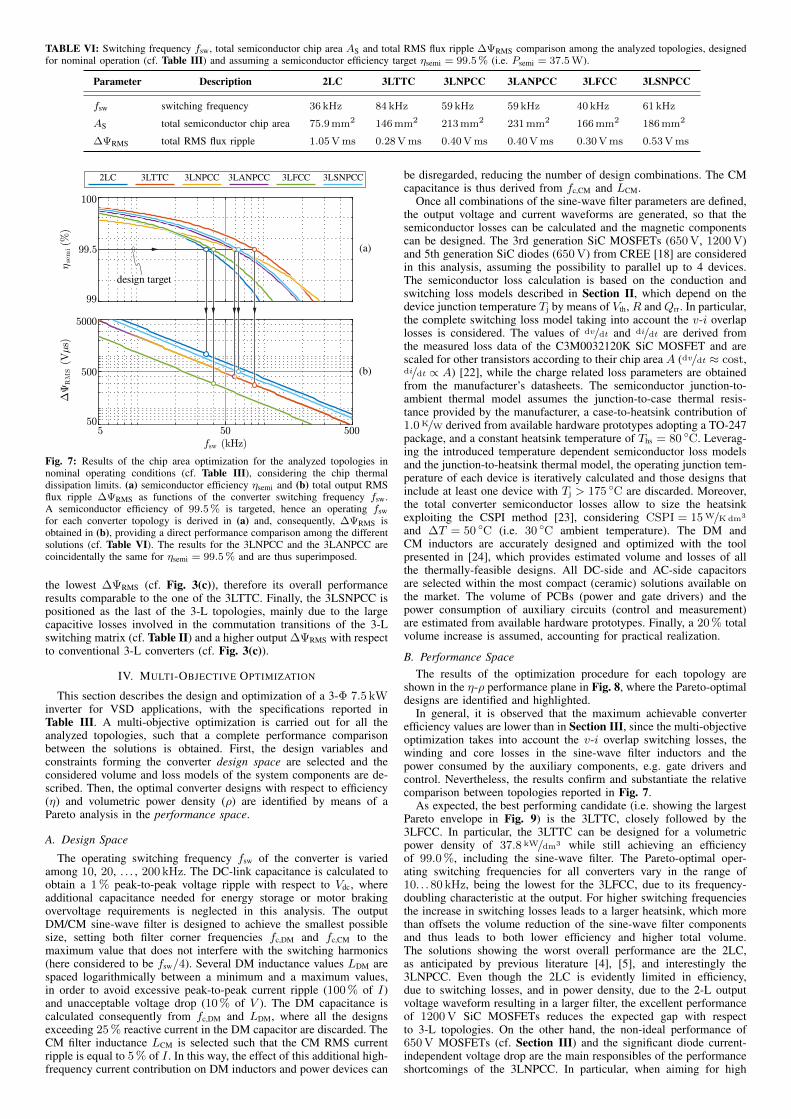
TABLE VI: Switching frequency fsw, total semiconductor chip area AS and total RMS flux ripple ∆ΨRMS comparison among the analyzed topologies, designedfor nominal operation (cf. Table III) and assuming a semiconductor efficiency target ηsemi = 99.5 % (i.e. Psemi = 37.5 W).
Parameter Description 2LC 3LTTC 3LNPCC 3LANPCC 3LFCC 3LSNPCC
fsw switching frequency 36 kHz 84 kHz 59 kHz 59 kHz 40 kHz 61 kHz
AS total semiconductor chip area 75.9 mm2 146 mm2 213 mm2 231 mm2 166 mm2 186 mm2
∆ΨRMS total RMS flux ripple 1.05 V ms 0.28 V ms 0.40 V ms 0.40 V ms 0.30 V ms 0.53 V ms
2LC 3LTTC 3LNPCC 3LANPCC 3LFCC 3LSNPCC
(b)
design target
(a)
Fig. 7: Results of the chip area optimization for the analyzed topologies innominal operating conditions (cf. Table III), considering the chip thermaldissipation limits. (a) semiconductor efficiency ηsemi and (b) total output RMSflux ripple ∆ΨRMS as functions of the converter switching frequency fsw.A semiconductor efficiency of 99.5 % is targeted, hence an operating fswfor each converter topology is derived in (a) and, consequently, ∆ΨRMS isobtained in (b), providing a direct performance comparison among the differentsolutions (cf. Table VI). The results for the 3LNPCC and the 3LANPCC arecoincidentally the same for ηsemi = 99.5 % and are thus superimposed.
the lowest ∆ΨRMS (cf. Fig. 3(c)), therefore its overall performanceresults comparable to the one of the 3LTTC. Finally, the 3LSNPCC ispositioned as the last of the 3-L topologies, mainly due to the largecapacitive losses involved in the commutation transitions of the 3-Lswitching matrix (cf. Table II) and a higher output ∆ΨRMS with respectto conventional 3-L converters (cf. Fig. 3(c)).
IV. MULTI-OBJECTIVE OPTIMIZATION
This section describes the design and optimization of a 3-Φ 7.5 kWinverter for VSD applications, with the specifications reported inTable III. A multi-objective optimization is carried out for all theanalyzed topologies, such that a complete performance comparisonbetween the solutions is obtained. First, the design variables andconstraints forming the converter design space are selected and theconsidered volume and loss models of the system components are de-scribed. Then, the optimal converter designs with respect to efficiency(η) and volumetric power density (ρ) are identified by means of aPareto analysis in the performance space.
A. Design Space
The operating switching frequency fsw of the converter is variedamong 10, 20, . . . , 200 kHz. The DC-link capacitance is calculated toobtain a 1 % peak-to-peak voltage ripple with respect to Vdc, whereadditional capacitance needed for energy storage or motor brakingovervoltage requirements is neglected in this analysis. The outputDM/CM sine-wave filter is designed to achieve the smallest possiblesize, setting both filter corner frequencies fc,DM and fc,CM to themaximum value that does not interfere with the switching harmonics(here considered to be fsw/4). Several DM inductance values LDM arespaced logarithmically between a minimum and a maximum values,in order to avoid excessive peak-to-peak current ripple (100 % of I)and unacceptable voltage drop (10 % of V ). The DM capacitance iscalculated consequently from fc,DM and LDM, where all the designsexceeding 25 % reactive current in the DM capacitor are discarded. TheCM filter inductance LCM is selected such that the CM RMS currentripple is equal to 5 % of I . In this way, the effect of this additional high-frequency current contribution on DM inductors and power devices can
be disregarded, reducing the number of design combinations. The CMcapacitance is thus derived from fc,CM and LCM.
Once all combinations of the sine-wave filter parameters are defined,the output voltage and current waveforms are generated, so that thesemiconductor losses can be calculated and the magnetic componentscan be designed. The 3rd generation SiC MOSFETs (650 V, 1200 V)and 5th generation SiC diodes (650 V) from CREE [18] are consideredin this analysis, assuming the possibility to parallel up to 4 devices.The semiconductor loss calculation is based on the conduction andswitching loss models described in Section II, which depend on thedevice junction temperature Tj by means of Vth, R and Qrr. In particular,the complete switching loss model taking into account the v-i overlaplosses is considered. The values of dv/dt and di/dt are derived fromthe measured loss data of the C3M0032120K SiC MOSFET and arescaled for other transistors according to their chip area A (dv/dt ≈ cost,di/dt ∝ A) [22], while the charge related loss parameters are obtainedfrom the manufacturer’s datasheets. The semiconductor junction-to-ambient thermal model assumes the junction-to-case thermal resis-tance provided by the manufacturer, a case-to-heatsink contribution of1.0 K/W derived from available hardware prototypes adopting a TO-247package, and a constant heatsink temperature of Ths = 80 C. Leverag-ing the introduced temperature dependent semiconductor loss modelsand the junction-to-heatsink thermal model, the operating junction tem-perature of each device is iteratively calculated and those designs thatinclude at least one device with Tj > 175 C are discarded. Moreover,the total converter semiconductor losses allow to size the heatsinkexploiting the CSPI method [23], considering CSPI = 15 W/Kdm3
and ∆T = 50 C (i.e. 30 C ambient temperature). The DM andCM inductors are accurately designed and optimized with the toolpresented in [24], which provides estimated volume and losses of allthe thermally-feasible designs. All DC-side and AC-side capacitorsare selected within the most compact (ceramic) solutions available onthe market. The volume of PCBs (power and gate drivers) and thepower consumption of auxiliary circuits (control and measurement)are estimated from available hardware prototypes. Finally, a 20 % totalvolume increase is assumed, accounting for practical realization.
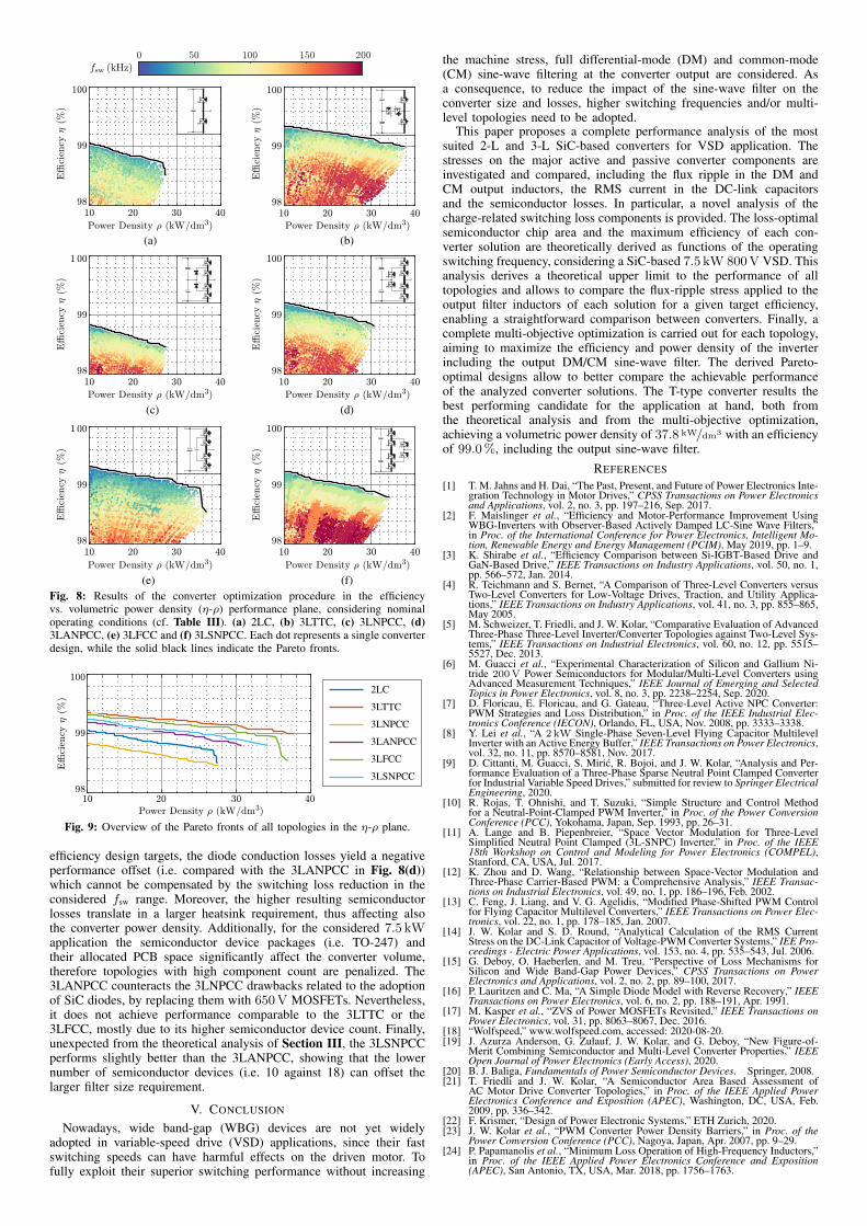
B. Performance SpaceThe results of the optimization procedure for each topology are
shown in the η-ρ performance plane in Fig. 8, where the Pareto-optimaldesigns are identified and highlighted.
In general, it is observed that the maximum achievable converterefficiency values are lower than in Section III, since the multi-objectiveoptimization takes into account the v-i overlap switching losses, thewinding and core losses in the sine-wave filter inductors and thepower consumed by the auxiliary components, e.g. gate drivers andcontrol. Nevertheless, the results confirm and substantiate the relativecomparison between topologies reported in Fig. 7.
As expected, the best performing candidate (i.e. showing the largestPareto envelope in Fig. 9) is the 3LTTC, closely followed by the3LFCC. In particular, the 3LTTC can be designed for a volumetricpower density of 37.8 kW/dm3 while still achieving an efficiencyof 99.0 %, including the sine-wave filter. The Pareto-optimal oper-ating switching frequencies for all converters vary in the range of10. . . 80 kHz, being the lowest for the 3LFCC, due to its frequency-doubling characteristic at the output. For higher switching frequenciesthe increase in switching losses leads to a larger heatsink, which morethan offsets the volume reduction of the sine-wave filter componentsand thus leads to both lower efficiency and higher total volume.The solutions showing the worst overall performance are the 2LC,as anticipated by previous literature [4], [5], and interestingly the3LNPCC. Even though the 2LC is evidently limited in efficiency,due to switching losses, and in power density, due to the 2-L outputvoltage waveform resulting in a larger filter, the excellent performanceof 1200 V SiC MOSFETs reduces the expected gap with respectto 3-L topologies. On the other hand, the non-ideal performance of650 V MOSFETs (cf. Section III) and the significant diode current-independent voltage drop are the main responsibles of the performanceshortcomings of the 3LNPCC. In particular, when aiming for high
(a)
(c) (d)
(e) (f)
(b)
Fig. 8: Results of the converter optimization procedure in the efficiencyvs. volumetric power density (η-ρ) performance plane, considering nominaloperating conditions (cf. Table III). (a) 2LC, (b) 3LTTC, (c) 3LNPCC, (d)3LANPCC, (e) 3LFCC and (f) 3LSNPCC. Each dot represents a single converterdesign, while the solid black lines indicate the Pareto fronts.
2LC
3LTTC
3LNPCC
3LANPCC
3LFCC
3LSNPCC
Fig. 9: Overview of the Pareto fronts of all topologies in the η-ρ plane.
efficiency design targets, the diode conduction losses yield a negativeperformance offset (i.e. compared with the 3LANPCC in Fig. 8(d))which cannot be compensated by the switching loss reduction in theconsidered fsw range. Moreover, the higher resulting semiconductorlosses translate in a larger heatsink requirement, thus affecting alsothe converter power density. Additionally, for the considered 7.5 kWapplication the semiconductor device packages (i.e. TO-247) andtheir allocated PCB space significantly affect the converter volume,therefore topologies with high component count are penalized. The3LANPCC counteracts the 3LNPCC drawbacks related to the adoptionof SiC diodes, by replacing them with 650 V MOSFETs. Nevertheless,it does not achieve performance comparable to the 3LTTC or the3LFCC, mostly due to its higher semiconductor device count. Finally,unexpected from the theoretical analysis of Section III, the 3LSNPCCperforms slightly better than the 3LANPCC, showing that the lowernumber of semiconductor devices (i.e. 10 against 18) can offset thelarger filter size requirement.
V. CONCLUSION
Nowadays, wide band-gap (WBG) devices are not yet widelyadopted in variable-speed drive (VSD) applications, since their fastswitching speeds can have harmful effects on the driven motor. Tofully exploit their superior switching performance without increasing
the machine stress, full differential-mode (DM) and common-mode(CM) sine-wave filtering at the converter output are considered. Asa consequence, to reduce the impact of the sine-wave filter on theconverter size and losses, higher switching frequencies and/or multi-level topologies need to be adopted.
This paper proposes a complete performance analysis of the mostsuited 2-L and 3-L SiC-based converters for VSD application. Thestresses on the major active and passive converter components areinvestigated and compared, including the flux ripple in the DM andCM output inductors, the RMS current in the DC-link capacitorsand the semiconductor losses. In particular, a novel analysis of thecharge-related switching loss components is provided. The loss-optimalsemiconductor chip area and the maximum efficiency of each con-verter solution are theoretically derived as functions of the operatingswitching frequency, considering a SiC-based 7.5 kW 800 V VSD. Thisanalysis derives a theoretical upper limit to the performance of alltopologies and allows to compare the flux-ripple stress applied to theoutput filter inductors of each solution for a given target efficiency,enabling a straightforward comparison between converters. Finally, acomplete multi-objective optimization is carried out for each topology,aiming to maximize the efficiency and power density of the inverterincluding the output DM/CM sine-wave filter. The derived Pareto-optimal designs allow to better compare the achievable performanceof the analyzed converter solutions. The T-type converter results thebest performing candidate for the application at hand, both fromthe theoretical analysis and from the multi-objective optimization,achieving a volumetric power density of 37.8 kW/dm3 with an efficiencyof 99.0 %, including the output sine-wave filter.
REFERENCES
[1] T. M. Jahns and H. Dai, “The Past, Present, and Future of Power Electronics Inte-gration Technology in Motor Drives,” CPSS Transactions on Power Electronicsand Applications, vol. 2, no. 3, pp. 197–216, Sep. 2017.
[2] F. Maislinger et al., “Efficiency and Motor-Performance Improvement UsingWBG-Inverters with Observer-Based Actively Damped LC-Sine Wave Filters,”in Proc. of the International Conference for Power Electronics, Intelligent Mo-tion, Renewable Energy and Energy Management (PCIM), May 2019, pp. 1–9.
[3] K. Shirabe et al., “Efficiency Comparison between Si-IGBT-Based Drive andGaN-Based Drive,” IEEE Transactions on Industry Applications, vol. 50, no. 1,pp. 566–572, Jan. 2014.
[4] R. Teichmann and S. Bernet, “A Comparison of Three-Level Converters versusTwo-Level Converters for Low-Voltage Drives, Traction, and Utility Applica-tions,” IEEE Transactions on Industry Applications, vol. 41, no. 3, pp. 855–865,May 2005.
[5] M. Schweizer, T. Friedli, and J. W. Kolar, “Comparative Evaluation of AdvancedThree-Phase Three-Level Inverter/Converter Topologies against Two-Level Sys-tems,” IEEE Transactions on Industrial Electronics, vol. 60, no. 12, pp. 5515–5527, Dec. 2013.
[6] M. Guacci et al., “Experimental Characterization of Silicon and Gallium Ni-tride 200V Power Semiconductors for Modular/Multi-Level Converters usingAdvanced Measurement Techniques,” IEEE Journal of Emerging and SelectedTopics in Power Electronics, vol. 8, no. 3, pp. 2238–2254, Sep. 2020.
[7] D. Floricau, E. Floricau, and G. Gateau, “Three-Level Active NPC Converter:PWM Strategies and Loss Distribution,” in Proc. of the IEEE Industrial Elec-tronics Conference (IECON), Orlando, FL, USA, Nov. 2008, pp. 3333–3338.
[8] Y. Lei et al., “A 2 kW Single-Phase Seven-Level Flying Capacitor MultilevelInverter with an Active Energy Buffer,” IEEE Transactions on Power Electronics,vol. 32, no. 11, pp. 8570–8581, Nov. 2017.
[9] D. Cittanti, M. Guacci, S. Miric, R. Bojoi, and J. W. Kolar, “Analysis and Per-formance Evaluation of a Three-Phase Sparse Neutral Point Clamped Converterfor Industrial Variable Speed Drives,” submitted for review to Springer ElectricalEngineering, 2020.
[10] R. Rojas, T. Ohnishi, and T. Suzuki, “Simple Structure and Control Methodfor a Neutral-Point-Clamped PWM Inverter,” in Proc. of the Power ConversionConference (PCC), Yokohama, Japan, Sep. 1993, pp. 26–31.
[11] A. Lange and B. Piepenbreier, “Space Vector Modulation for Three-LevelSimplified Neutral Point Clamped (3L-SNPC) Inverter,” in Proc. of the IEEE18th Workshop on Control and Modeling for Power Electronics (COMPEL),Stanford, CA, USA, Jul. 2017.
[12] K. Zhou and D. Wang, “Relationship between Space-Vector Modulation andThree-Phase Carrier-Based PWM: a Comprehensive Analysis,” IEEE Transac-tions on Industrial Electronics, vol. 49, no. 1, pp. 186–196, Feb. 2002.
[13] C. Feng, J. Liang, and V. G. Agelidis, “Modified Phase-Shifted PWM Controlfor Flying Capacitor Multilevel Converters,” IEEE Transactions on Power Elec-tronics, vol. 22, no. 1, pp. 178–185, Jan. 2007.
[14] J. W. Kolar and S. D. Round, “Analytical Calculation of the RMS CurrentStress on the DC-Link Capacitor of Voltage-PWM Converter Systems,” IEE Pro-ceedings - Electric Power Applications, vol. 153, no. 4, pp. 535–543, Jul. 2006.
[15] G. Deboy, O. Haeberlen, and M. Treu, “Perspective of Loss Mechanisms forSilicon and Wide Band-Gap Power Devices,” CPSS Transactions on PowerElectronics and Applications, vol. 2, no. 2, pp. 89–100, 2017.
[16] P. Lauritzen and C. Ma, “A Simple Diode Model with Reverse Recovery,” IEEETransactions on Power Electronics, vol. 6, no. 2, pp. 188–191, Apr. 1991.
[17] M. Kasper et al., “ZVS of Power MOSFETs Revisited,” IEEE Transactions onPower Electronics, vol. 31, pp. 8063–8067, Dec. 2016.
[18] “Wolfspeed,” www.wolfspeed.com, accessed: 2020-08-20.[19] J. Azurza Anderson, G. Zulauf, J. W. Kolar, and G. Deboy, “New Figure-of-
Merit Combining Semiconductor and Multi-Level Converter Properties,” IEEEOpen Journal of Power Electronics (Early Access), 2020.
[20] B. J. Baliga, Fundamentals of Power Semiconductor Devices. Springer, 2008.[21] T. Friedli and J. W. Kolar, “A Semiconductor Area Based Assessment of
AC Motor Drive Converter Topologies,” in Proc. of the IEEE Applied PowerElectronics Conference and Exposition (APEC), Washington, DC, USA, Feb.2009, pp. 336–342.
[22] F. Krismer, “Design of Power Electronic Systems,” ETH Zurich, 2020.[23] J. W. Kolar et al., “PWM Converter Power Density Barriers,” in Proc. of the
Power Conversion Conference (PCC), Nagoya, Japan, Apr. 2007, pp. 9–29.[24] P. Papamanolis et al., “Minimum Loss Operation of High-Frequency Inductors,”
in Proc. of the IEEE Applied Power Electronics Conference and Exposition(APEC), San Antonio, TX, USA, Mar. 2018, pp. 1756–1763.