Company Profile · · 2016-12-16devices and services to answer unmet medical needs at each stage...
36
Company Profile 2016
Transcript of Company Profile · · 2016-12-16devices and services to answer unmet medical needs at each stage...

Company Profile 2016

2
Contents
3 Nikon’s Philosophy and Vision
4 Message from the President
6 Nikon’s Aim: Technology that Inspires the Spirit
8 Nikon’s Aim: Technology that Moves Society Forward
10 Overview of Nikon Businesses
12 Precision Equipment Business
14 Imaging Products Business
16 Instruments Business
18 Medical Business
19 Other Businesses
20 Global Network
22 Marketing
24 Research and Development
26 Manufacturing
28 Sustainability
30 Environmental Activities
32 Social Contribution and Cultural Activities
34 Corporate History

3
Nikon’s Philosophy and Vision
Our Philosophy
Our Aspirations
Our Commitments
These are the everyday policies we live by to realize our aspirations.
“Our Aspirations” mean not only to meet the needs of customers but also to provide customers with new value that exceeds their expectations. “Meeting needs. Exceeding expectations.” is our vision for the future.
Our corporate philosophy is “Trustworthiness and Creativity.” These are simple words, but they are not easily put into practice. These important words represent unchanging principles to which we will always be dedicated.
Trustworthiness and Creativity
Meeting needs. Exceeding expectations.
Be proactive Be broad-minded and well-informed in order to act quickly and resolutely.
Communicate well Harmonize diverse skills by thinking out of the box and communicating effectively with others.
Seek new knowledge Pioneer new potential through self-study and insatiable curiosity.
Display integrity Work with diligence and sincerity as a responsible individual.

4
As we celebrate our 100th anniversary in 2017, we are truly grateful for your continuous support and guidance. Since the company was established in 1917, Nikon has cultivated its status as a pioneer of optical technologies. Guided by our corporate philosophy of “Trustworthiness and Creativity,” we have continued to challenge ourselves to provide a wide range of products and services globally by harnessing our advanced technologies, the core of which encompasses opto-electronics and precision technologies.
The global business environment has experienced drastic changes in the last few years. Rapid advancement in the field of information technology has helped expedite the installation of new networking infrastructure around the world. As it becomes possible to process more and more data at ever-faster speeds, information technologies continue to change how we do business and how we live our lives. Companies should not merely be satisfied with variations of conventional ideas. They must also have the creativity to proactively identify perpetually changing market needs, as well as the agility to quickly respond to changes.
With society facing a historic transition comparable to the Industrial Revolution, we at Nikon are making a major shift, from a corporate culture that largely depends on hardware to an enterprise that proposes business solutions, while keeping focused on “Trustworthiness and Creativity” as our manufacturing philosophy. Changing the mindset of each of our staff members is of the utmost importance. We are emphasizing three values in particular — “Curiosity” to explore out-of-the-box possibilities, “Open Mind” to flexibly accept opinions from other fields, and “Power to Inspire” that is essential for guiding and motivating groups that work together.
By encouraging staff members to proactively engage with customers and discover new needs, Nikon will be much better equipped to propose appropriate business solutions. By repeating this cycle, we are determined to expand our business fields and become an ideal company from which society will have higher expectations.
This year marks the halfway point of Nikon’s Medium Term Management Plan, announced in May 2015. Our goal is to exhibit progress not only in our instruments and medical businesses — the two fields we expect to grow — but in all of our businesses, including precision equipment and imaging products.
We ask for your continued support and guidance on this exciting journey.
Kazuo UshidaPresident
Representative Director
Accelerating our transformation toward a new and reformed Nikon

5
Message from the President

6
Shoot superior pictures.
Experience the vividness of nature up close.
Enjoy large-screen, high-definition television with
family and friends.
Broaden communications with high-performance,
easy-to-use personal computers and smartphones.
Exciting encounters with new products and services
will realize people’s dreams.
Nikon’s technology will be there.
Exciting Encounters

7
Nikon’s Aim: Technology that Inspires the Spirit

8

9
Nikon’s Aim: Technology that Moves Society Forward
How far will IC integration go?
Will cameras equal — or surpass the human eye?
How clear will the mechanism of life become?
How far can we peer into outer space?
Our incessant advance toward dreams and our
unwavering spirit for research will open the doors
to the future.
Nikon’s technology will be there.
Uncompromising Technology

10
Nikon is contributing to technology in numerous fields, from manufacturing semiconductors with nanometer-rule circuit patterns and advancing bioscience, to furthering the possibilities of imaging and capturing views of stars that are billions of light years away. What makes this possible? Our opto-electronics and precision technologies that we have nurtured throughout our history and used to create an extensive range of products, services and even more new technologies. Nikon will continue to enrich lives around the world, support cutting-edge industries that are shaping the future, and confront the challenges facing societies around the world.
Nikon technologies contribute to people’s lives and future dreams.
Precision Equipment Business
Semiconductor Lithography BusinessFPD Lithography Business
Precision Equipment Business
Imaging Products Business
Imaging Products Business
Modern society reaps great benefits from the electronics fabricated in industrial sectors, including areas such as home appliances, personal computers and automobiles. Nikon is continuously advancing the production of semiconductor lithography systems that are used to manufacture semiconductors — the very core of electronics — as well as FPD lithography systems for manufacturing liquid crystal panels and organic light-emitting diode (OLED) panels that are indispensable to LCD TVs, computers, and smartphones. In these and many other ways, Nikon is fostering and innovating our electronics-based society.
Thanks to advances in digital technology, the camera has evolved into an everyday device anybody can use to easily take high-quality pictures. For professional photographers, digital camera technologies have yielded remarkably advanced functions and performance that can significantly intensify creativity and expression. Nikon camera production acumen and technologies, both supported by our long history, will continue to expand imaging possibilities.
•Semiconductor lithography systems •FPD lithography systems
•Digital cameras •Film cameras •Interchangeable lenses •Speedlights •Photographic accessories •Software •Sport optics
Opto-electronics Technologies
Precision Technologies
P12-13
P14-15

11
Microscope Solutions BusinessIndustrial Metrology Business
Customized Products BusinessGlass BusinessEncoders BusinessOphthalmic Lenses Business
Instruments Business
Instruments Business
Medical Business
Other Businesses Other Businesses
Medical Business
Microscopes and measuring instruments from our Instruments Business arecontributing to fields ranging from bioscience research to industrial sectors such as components for electronics, automobiles and aircraft. We also offer sophisticated, high-caliber surveying instruments used in architectural design and urban planning. Nikon supports the development of society with precision technologies and eyes firmly focused on the micro level.
Building upon Nikon’s core competencies of opto-electronics and precision technologies, we are developing new technologies, devices and services to answer unmet medical needs at each stage — prevention, diagnosis, treatment and prognosis management.
The development of our business makes full use of the many technologies that Nikon has accumulated over the years. In addition to precision equipment, imaging products, instruments and the medical field, Nikon businesses encompass familiar items like ophthalmic lenses, more specialized goods such as industrial optical materials, encoders that are indispensable for factory automation, and the cutting-edge technology utilized in space exploration. Through these businesses, we continue to facilitate the evolution of science, technology, industry and society.
•Biological microscopes •Industrial microscopes •Stereoscopic microscopes•Measuring instruments •X-ray/CT inspection systems •Surveying instruments
•Retinal diagnostic imaging equipment
•Customized Products Business •Glass Business •Encoders Business •Ophthalmic Lenses Business
Precision Technologies
P16-17
P18
19
Overview of Nikon Businesses
12
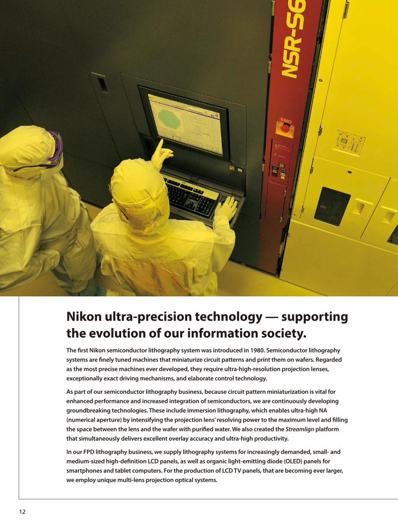
The first Nikon semiconductor lithography system was introduced in 1980. Semiconductor lithography systems are finely tuned machines that miniaturize circuit patterns and print them on wafers. Regarded as the most precise machines ever developed, they require ultra-high-resolution projection lenses, exceptionally exact driving mechanisms, and elaborate control technology.
As part of our semiconductor lithography business, because circuit pattern miniaturization is vital for enhanced performance and increased integration of semiconductors, we are continuously developing groundbreaking technologies. These include immersion lithography, which enables ultra-high NA (numerical aperture) by intensifying the projection lens’ resolving power to the maximum level and filling the space between the lens and the wafer with purified water. We also created the Streamlign platform that simultaneously delivers excellent overlay accuracy and ultra-high productivity.
In our FPD lithography business, we supply lithography systems for increasingly demanded, small- and medium-sized high-definition LCD panels, as well as organic light-emitting diode (OLED) panels for smartphones and tablet computers. For the production of LCD TV panels, that are becoming ever larger, we employ unique multi-lens projection optical systems.
Nikon ultra-precision technology — supporting the evolution of our information society.

13
The FX-68S supports the production of leading-edge, high-resolution, small- and medium-sized panels from Gen 6 plates. The scanner method enables improved productivity, excellent resolution (1.5μm) and high alignment accuracy simultaneously.
By incorporating the Streamlign platform, performance of which was proven in immersion scanners, this scanner achieves enhanced overlay accuracy and higher throughput. This improved performance addresses customers’ needs for increased accuracy and stable production in cutting-edge device manufacturing.
Employing the Streamlign platform, this scanner was developed for high-volume manufacturing of devices at the 7 nm process node (capable of handling multiple patterning). The super-high accuracy of below 2.3 nm Mix-and-Match Overlay (MMO) and extremely high throughput of more than 270 wafers per hour (96 shots) contribute to stable volume manufacturing at cutting-edge production lines.
Using the multi-lens projection optical system, the FX-101S is capable of handling Gen 10 large glass plates, which measure about 3 x 3 m. Single-scan printing produces six to eight large panels of over 60 inches screen size, making it an excellent solution for mass production.
ArF Immersion Scanner
NSR-S631EArF Scanner
NSR-S322F
FPD Scanner
FX-68SFPD Scanner
FX-101S
Precision Equipment Business
Products of FPD Lithography Business
Products of Semiconductor Lithography Business

14
Digital cameras are further expanding imaging possibilities, including shooting, viewing, processing and sharing. Nikon has been developing high-performance products by combining the latest digital image-processing and network technologies with Nikon film camera technology, whose fame has long been established since the Nikon Model I small-sized camera launched in 1948. By doing this, we not only meet an ever-increasing array of demands with a broad lineup range from cameras for family use to those for professional photographers, but also greatly enhance the world’s photographic culture.
Other products offer pleasures unique to digital imaging: image-editing software, online photo sharing service NIKON IMAGE SPACE, and service app SnapBridge that seamlessly connects a Nikon camera and smart device. We also extend the joy of viewing by offering binoculars, Fieldscopes and loupes, as well as laser rangefinders for use in golf.
Greater joys of imaging for more people.

15
The EDG 85 VR Series is the world’s first* Fieldscope to incorporate Nikon’s lens-shift type VR (Vibration Reduction) system. This system maximizes the EDG Fieldscope’s performance, ensuring comfortable, stress-free viewing.
Comprising our flagship models, the EDG series binoculars employ leading-edge optical technologies. For instance, EDG binoculars utilize Nikon’s renowned ED (Extra-low Dispersion) glass, as well as a field-flattener lens system. Now, you can enjoy a sharp, contrast-rich and clear image throughout the entire field of view.
This is a lightweight and compact laser rangefinder that is ideal for golf. Employing ID Technology, it displays the slope adjusted distance, which provides a guide to how far you should hit the ball and is especially useful when golfing on an uphill/downhill course. Nikon’s First Target Priority Algorithm enables you to measure to the flagstick easily.
Our wide lineup of interchangeable lenses — from super-wide-angle lenses and super- telephoto lenses to fisheye and micro lenses — meets the diverse needs of our customers, from entry-level users to professional photographers. NIKKOR lenses beautifully capture subjects with superb depiction thanks to our unique knowhow and cutting-edge technology.
The world’s smallest and lightest in the class*1, this easy-to-carry camera packs a 60x optical zoom covering from wide-angle 24 mm to super-telephoto 1440 mm (35mm [135] format equivalent) as well as up to 120x*2 Dynamic Fine Zoom*3. The B700 also provides a camera-shake compensation effect equivalent to 5.0 stops*4 thanks to Dual Detect Optical VR and a shooting time lag of approx. 0.10 s*5.
Incorporating an image sensor and NIKKOR lens on both sides, this wearable action camera provides 360° video recording in superb image quality of 4K UHD with a sense of immersion. Featuring waterproof performance to a depth of 30 m without housing attached, as well as shock-, dust- and cold-resistant capabilities, it realizes superior operability and mobility under diverse shooting conditions in outdoor sports and leisure scenes.
The Nikon 1 J5 features 20.8 effective megapixels, newly developed backside illumination CMOS image sensor and the new EXPEED 5A image-processing engine in a simple and modern body offering a sense of high quality and superboperability. While achieving the world’s fastest*1 continuous shooting frame rate at approx. 20 fps with AF and the world’s shortest*2 shooting time lag, this camera enables 4K UHD movie recording — a first for Nikon digital cameras. A tilting monitor that facilitates self-portraits is also adopted.
Featuring an all-new 153-point AF system and high-speed continuous shooting at approx. 12 fps* with full-time AF and AE, the D5 demonstrates superb subject acquisition in a variety of situations. A newly developed Nikon FX-format CMOS sensor and advanced EXPEED 5 image-processing engine contribute to achieving standard sensitivity up to ISO 102400 — the highest in Nikon’s history. This flagship model is designed to further expand shooting possibilities for all professional photographers.* Assumes a shutter speed of 1/250 s or faster in CH (continuous high) release mode.
*1 Among compact digital cameras with 60x or higher magnification zoom lenses available as of February 23, 2016. Statement based on Nikon research. *2 At the maximum image size. May vary according to image size.*3 Magnification of Dynamic Fine Zoom is calculated from the maximum wide-angle position of optical zoom.*4 Based on CIPA Standards; measured at approx. 350 mm (35mm [135] format equivalent).*5 Based on CIPA Guidelines; measured at maximum wide-angle position, subject brightness LV10, in Programmed auto exposure mode and manual (normal) mode as focus-area selection.
*1 Among digital cameras with interchangeable lenses available as of April 2, 2015. Statement based on Nikon research.*2 Among digital cameras with interchangeable lenses available as of April 2, 2015. Tested using the 1 NIKKOR VR 10-30mm f/3.5-5.6 PD-ZOOM at the maximum wide-angle position in Single-point AF mode. Statement based on Nikon research.
* Among fieldscopes as of October 2011.
Digital SLR Camera
D5
Advanced Camera with Interchangeable Lenses
Nikon 1 J5
Compact Digital Camera
COOLPIX B700
Action Camera
KeyMission 360
Interchangeable Lenses for SLR Cameras
NIKKOR
Binoculars
EDG 8x42
Fieldscope EDG 85-A VR
Laser Rangefinder
COOLSHOT 40i
Imaging Products Business

16
Our instruments business offers products and effective business solutions in diverse fields from bioscience to industry.
In the microscope solutions business, following a collaboration agreement with Lonza of Switzerland, we started contract manufacturing business of cells, etc. for regenerative medicine with a new, wholly owned subsidiary Nikon CeLL innovation Co., Ltd. We will advance toward expedited clinical application of regenerative medicine in Japan. Nikon also supports medical researchers with our Inverted Routine/Research Microscopes. Designed to increase efficiency, they provide images with natural contrast and depth, even of thick specimens.
Sophisticated manufacturing processes, like those employed for electronic components, automobiles and aircraft, demand exhaustive quality control. To this end, our industrial metrology business offers a variety of products, including industrial microscopes, measuring instruments and non-destructive/contact inspection systems. Furthermore, in the field of construction and surveying, Nikon-Trimble Co., Ltd., a joint venture between Nikon and U.S.-based Trimble Navigation Ltd., delivers high-precision surveying solutions that boost productivity.
Providing solutions to diverse problems from bioscience to industry.

17
N-STORM, which employs Stochastic Optical Reconstruction Microscopy technology licensed from Harvard University, has increased resolution to more than 10 times that of conventional optical microscopes. N-STORM delivers rich information that enhances understanding of the structure of living cells and biological phenomena at molecular levels.
This system utilizes X-ray transmission to display the inner structure of electronic components, injection moldings and castings for nondestructive inspection. Employing a high-power X-ray, the XT H 450 enables inspection of large castings and high-density metal objects, such as turbine blades. Providing internal images with the world’s highest level of resolution delivered by the powerful 450kV X-ray, the XT H 450 addresses increasing demand for more accurate industrial inspections.
Total stations are surveying instruments used to measure distance and angle. The smallest and lightest in its class, the Nivo series is especially effective in dangerous places such as steep slopes and high-rise construction sites. These units’ curved, ergonomic design is a dramatic departure from traditional surveying instruments.
N-SIM (Nikon’s Structured Illumination Microscopy), a combination of technology licensed by the University of California, San Francisco, and Nikon’s optical technology, allows observation of the minute intracellular structures of live cells with a resolution of approx. 100 nm — about double that of conventional optical microscopes.
Utilizing optical measuring technology and image processing performed by computer, this system automatically measures the dimensions and shapes of precision parts and electronic components, as well as transparent workpieces and those of complex design. Embedded with Nikon’s exclusive linear encoder, it achieves highly accurate measurement.
As a non-contact 3D metrology system, the HN-C3030 offers the world’s most precise*, high-speed measuring in a compact body. The device quickly acquires various data of the target such as surface form, surface waviness, abrasion, deformation and subtle unevenness, that have been difficult to determine conventionally.
The Ts2R (right) for research effectively benefits biological and medical laboratories at academic and corporate institutions due to its compatibility with diverse observation methods and easy operation. Providing increased efficiency for microscopy with its superb optical performance and operation, the Ts2 (left) also greatly contributes to cell culture observation, a vital element of basic research.
The BioStation CT allows time-lapse observation of cells while they are being cultured in the stable environment of an incubator. This not only mitigates the burden placed on researchers, but simultaneously enables tracking observation of cells without inflicting stress on them.
Super Resolution Microscope
N-SIMSuper Resolution Microscope
N-STORM 4.0Inverted Microscopes
ECLIPSE Ts2/Ts2R
CNC Video Measuring System
NEXIV VMZ-R4540
X-ray/CT Inspection System
XT H 450
Cell Culture Observation System
BioStation CT
Non-Contact Multi-Sensor 3D Metrology System
HN-C3030
Total Station
Nivo Series
Instruments Business
Products of Industrial Metrology Business
Products of Microscope Solutions Business
* Statement based on Nikon research as of October 23, 2014.

18
With its wide field of view of 200°, the California captures an image covering more than 80% of the retinal area in non-mydriatic, non-contact photography. It allows easy detection of symptoms appearing in peripherals — that have previously been difficult to spot. Its compact, table-top body offers increased flexibility of installation.
Medical Business
Building upon Nikon’s core competencies of opto-electronics and precision technologies, we are developing a new medical device business to answer unmet medical needs at each stage — prevention, diagnosis, treatment and prognosis management. In April 2014, Nikon formed a business alliance with LSI Medience (previously Mitsubishi Chemical Medience Corporation), working toward development and commercialization of small-size Point of Care Testing (POCT) devices. Furthermore, in May 2015, we acquired Optos Plc, a leading company in the retinal diagnostic imaging equipment market, as a wholly owned subsidiary. This creates the opportunity to broaden our business base in the field of retina regenerative medicine.
New contribution to the healthcare and medical field.
Retinal diagnostic imaging equipmentCalifornia
19
State-of-the-art Technologies for Space
Other Businesses
Since our founding, Nikon has applied our opto-electronics and precision technologies to meet many of society’s needs. Our efforts have borne much fruit: cameras, semiconductor lithography systems, microscopes, cutting-edge technologies involved in space development and many other products and systems vital for people’s lives and industry. We have been able to achieve all this because we have always looked at the future of people’s lives and society, developing new products and unique technologies that not only meet needs, but expand our business.
New contribution to the healthcare and medical field.
Core technologies bear much fruit.
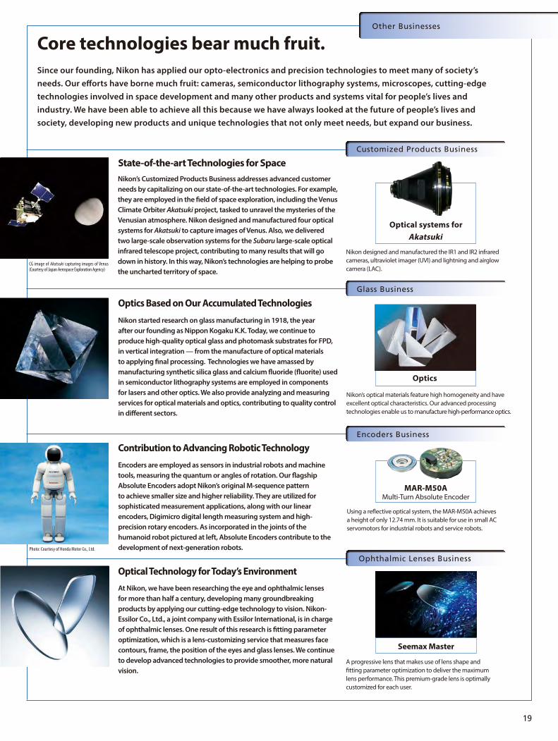
Nikon designed and manufactured the IR1 and IR2 infrared cameras, ultraviolet imager (UVI) and lightning and airglow camera (LAC).
Using a reflective optical system, the MAR-M50A achieves a height of only 12.74 mm. It is suitable for use in small AC servomotors for industrial robots and service robots.
Nikon’s optical materials feature high homogeneity and have excellent optical characteristics. Our advanced processing technologies enable us to manufacture high-performance optics.
A progressive lens that makes use of lens shape and fitting parameter optimization to deliver the maximum lens performance. This premium-grade lens is optimally customized for each user.
Contribution to Advancing Robotic Technology
Optics Based on Our Accumulated Technologies
Optical Technology for Today’s Environment
Nikon’s Customized Products Business addresses advanced customer needs by capitalizing on our state-of-the-art technologies. For example, they are employed in the field of space exploration, including the Venus Climate Orbiter Akatsuki project, tasked to unravel the mysteries of the Venusian atmosphere. Nikon designed and manufactured four optical systems for Akatsuki to capture images of Venus. Also, we delivered two large-scale observation systems for the Subaru large-scale optical infrared telescope project, contributing to many results that will go down in history. In this way, Nikon’s technologies are helping to probe the uncharted territory of space.
Encoders are employed as sensors in industrial robots and machine tools, measuring the quantum or angles of rotation. Our flagship Absolute Encoders adopt Nikon’s original M-sequence pattern to achieve smaller size and higher reliability. They are utilized for sophisticated measurement applications, along with our linear encoders, Digimicro digital length measuring system and high-precision rotary encoders. As incorporated in the joints of the humanoid robot pictured at left, Absolute Encoders contribute to the development of next-generation robots.
Nikon started research on glass manufacturing in 1918, the year after our founding as Nippon Kogaku K.K. Today, we continue to produce high-quality optical glass and photomask substrates for FPD, in vertical integration — from the manufacture of optical materials to applying final processing. Technologies we have amassed by manufacturing synthetic silica glass and calcium fluoride (fluorite) used in semiconductor lithography systems are employed in components for lasers and other optics. We also provide analyzing and measuring services for optical materials and optics, contributing to quality control in different sectors.
At Nikon, we have been researching the eye and ophthalmic lenses for more than half a century, developing many groundbreaking products by applying our cutting-edge technology to vision. Nikon-Essilor Co., Ltd., a joint company with Essilor International, is in charge of ophthalmic lenses. One result of this research is fitting parameter optimization, which is a lens-customizing service that measures face contours, frame, the position of the eyes and glass lenses. We continue to develop advanced technologies to provide smoother, more natural vision.
Photo: Courtesy of Honda Motor Co., Ltd.
CG image of Akatsuki capturing images of Venus (Courtesy of Japan Aerospace Exploration Agency)
Optical systems for Akatsuki
Optics
Seemax Master
MAR-M50AMulti-Turn Absolute Encoder
Glass Business
Encoders Business
Ophthalmic Lenses Business
Customized Products Business
20
Our technology, products and services contribute to everything from people’s everyday lives to space exploration. In order to supply our products where they are needed, we have established our production bases at strategic points, and have positioned our sales and service locations based on careful analysis of industrial and market characteristics, as well as cultures and lifestyles. By combining the comprehensive power of these groups and proposing business solutions, Nikon delivers our values to the whole world.
Delivering Nikon’s values to the world:Nikon globally expands its comprehensive power.
• Tochigi Nikon Precision Co., Ltd.• Nikon Tec Corporation• Miyagi Nikon Precision Co., Ltd.• Tochigi Nikon Corporation• Sendai Nikon Corporation• Nikon Imaging Japan Inc.• Nikon Vision Co., Ltd.• Kurobane Nikon Co., Ltd.• Nikon Instech Co., Ltd.• Nikon CeLL innovation Co., Ltd.• Nikon-Trimble Co., Ltd.• Nikon Engineering Co., Ltd.• Hikari Glass Co., Ltd.• Nikon-Essilor Co., Ltd.• Nikon Lenswear Experience Center Co., Ltd.• Nikon Business Service Co., Ltd.• Nikon Staff Service Corporation• Nikon Tsubasa Inc.• Nikon Systems Inc.• Nikon and Essilor International Joint Research Center Co., Ltd.
• Nikon Americas Inc.• Nikon Research Corporation of America• Nikon Precision Inc.• Nikon Inc.• Nikon Canada Inc.• Nikon Mexico, S.A. de C.V.• Nikon Latin America, S.A.• Nikon do Brasil Ltda.• Nikon Instruments Inc.• Nikon Metrology, Inc.
• Nikon Holdings Europe B.V.• Nikon Precision Europe GmbH• Nikon Europe B.V.• Nikon AG• Nikon GmbH• Nikon U.K. Ltd.• Nikon France S.A.S.• Nikon CEE GmbH• Nikon Kft.• Nikon s.r.o.• Nikon Polska Sp. z o.o.• Nikon (Russia) LLC.• Nikon Instruments Europe B.V.• Nikon Instruments S.p.A.• Nikon Metrology NV• Nikon Metrology GmbH• Nikon Metrology UK Ltd.• Nikon Metrology SARL• Optos Plc
• Nikon Holdings Hong Kong Limited• Nikon Asia Pacific Pte. Ltd.• Nikon Precision Korea Ltd.• Nikon Precision Taiwan Ltd.• Nikon Precision Shanghai Co., Ltd.• Nikon Hong Kong Ltd.• Nikon Singapore Pte. Ltd.• Nikon (Malaysia) Sdn. Bhd.• Nikon Australia Pty Ltd• Nikon India Private Limited• Nikon Sales (Thailand) Co., Ltd.• Nikon Middle East FZE• PT Nikon Indonesia• Nikon Imaging (China) Sales Co., Ltd.• Nikon Imaging Korea Co., Ltd.• Nikon (Thailand) Co., Ltd.• Nikon Imaging (China) Co., Ltd.• Nikon Lao Co., Ltd.• Nikon International Trading (Shenzhen) Co., Ltd.• Nikon Instruments (Shanghai) Co., Ltd.• Nikon Instruments Korea Co., Ltd.• Guang Dong Nikon Camera Co., Ltd.• Hang Zhou Nikon Camera Co., Ltd.• Nanjing Nikon Jiangnan Optical Instrument Co., Ltd.
Asia, Oceania, the Middle EastEuropeThe AmericasJapan

21
Global Network
Company Profile Ratio of Net Sales by Industry Segment(for the year ended March 31, 2016)
Ratio of Net Sales by Region(for the year ended March 31, 2016)
Precision Equipment22.2%
Japan 14.2%
United States 25.4%
Other 3.0%Instruments
9.4%
Medical 2.2%
Imaging Products63.2%
Europe20.5%
China17.0%
Other Areas22.9%
¥822,915million
¥822,915million
Company Name:Head Office:
PresidentRepresentative Director:Established:Capital:Net Sales:(consolidated)Number of Employees:(consolidated)Plants:
NIKON CORPORATIONShinagawa Intercity Tower C, 2-15-3, Konan, Minato-ku, Tokyo 108-6290 JapanTel: +81-3-6433-3600Kazuo UshidaJuly 25, 1917¥65,475 million (as of March 31, 2016)¥822,915 million (for the year ended March 31, 2016)25,729 (as of March 31, 2016)Oi, Yokohama, Sagamihara, Kumagaya, Mito and Yokosuka

22
Nikon’s product manufacturing process begins with us listening to people all over the world — people from different walks of life, people involved in different industries — so we can understand precisely what they want from us. We gather customers’ opinions in many different ways: sales, service and support activities, trade shows, promotional and other events, and via the Internet. To us, this information is invaluable. We are endeavoring to create new products and services that exceed customer expectations by aggregating and analyzing these opinions.
We listen to our customers and the voices of societies all over the world.
Supporting Professional PhotographersNikon Professional Services (NPS) is an organization that supports full-time professional-photographer members by providing various on-site assistance including service depots operating at international events. NPS responds to the exacting demands of professional photographers while applying their valuable feedback for product development. The photo above shows the NPS team from Nikon U.K. Ltd. in action.
Participation in Trade ShowsWe participate in many different kinds of trade shows around the world, using them as precious opportunities to explain our products to customers. The photo above shows Nikon Metrology NV’s booth at Control Germany*. Among the products we displayed were 3D metrology systems, 3D laser scanners, and X-ray/CT inspection systems.* The leading international trade fair for quality assurance, held at the Stuttgart Exhibition Centre.

23
Marketing
* An online shop operated by Nikon Imaging Japan Inc.
Product Planning by Nikon DirectNikon Direct* plans and sells products such as camera bags, accessories and photography clothing by analyzing customer feedback gathered via phone, e-mail and original marketing surveys. By creating unique products in response to customers’ tastes, Nikon Direct increases customer satisfaction.
Speedy Maintenance SystemNikon Tec Corporation is in charge of the maintenance of Nikon’s lithography systems in Japan. Most semiconductor and flat panel display production lines operate around the clock, so system failure significantly damages productivity. Field service engineers (FSE) provide prompt servicing to support the performance of our lithography systems, which have been called the most precise machines ever developed. Feedback from these engineers helps improve the reliability of our products.
Boosting Sales in Emerging MarketsTo facilitate better contact with our customers in emerging economies, we proactively set up sales subsidiaries as well as showrooms and service centers. We are making efforts to serve new customers by establishing marketing systems and conveying the appeal of the full range of our products. The photos show a showroom operated by Nikon India Private Limited (left) and another for industrial equipment operated by PT Nikon Indonesia (below).
24
Basic Technologies that Support Nikon
To strengthen our existing businesses and create new businesses, it is vital to continue basic R&D activities based on a long-term perspective. With our core technologies — opto-electronics and precision — as a foundation, Nikon is conducting R&D in wide-ranging areas of technologies, such as optics, precision measurement and manufacturing, image processing, materials, and software and systems. The Core Technology Division, that conducts these R&D activities, supports our businesses with research results and expertise. Each of our business units also engages in R&D activities to develop attractive products. Our R&D, ongoing since our founding, manifests itself in our technological prowess and forward-thinking products.
By mastering optics and precision technologies, we create a new future.
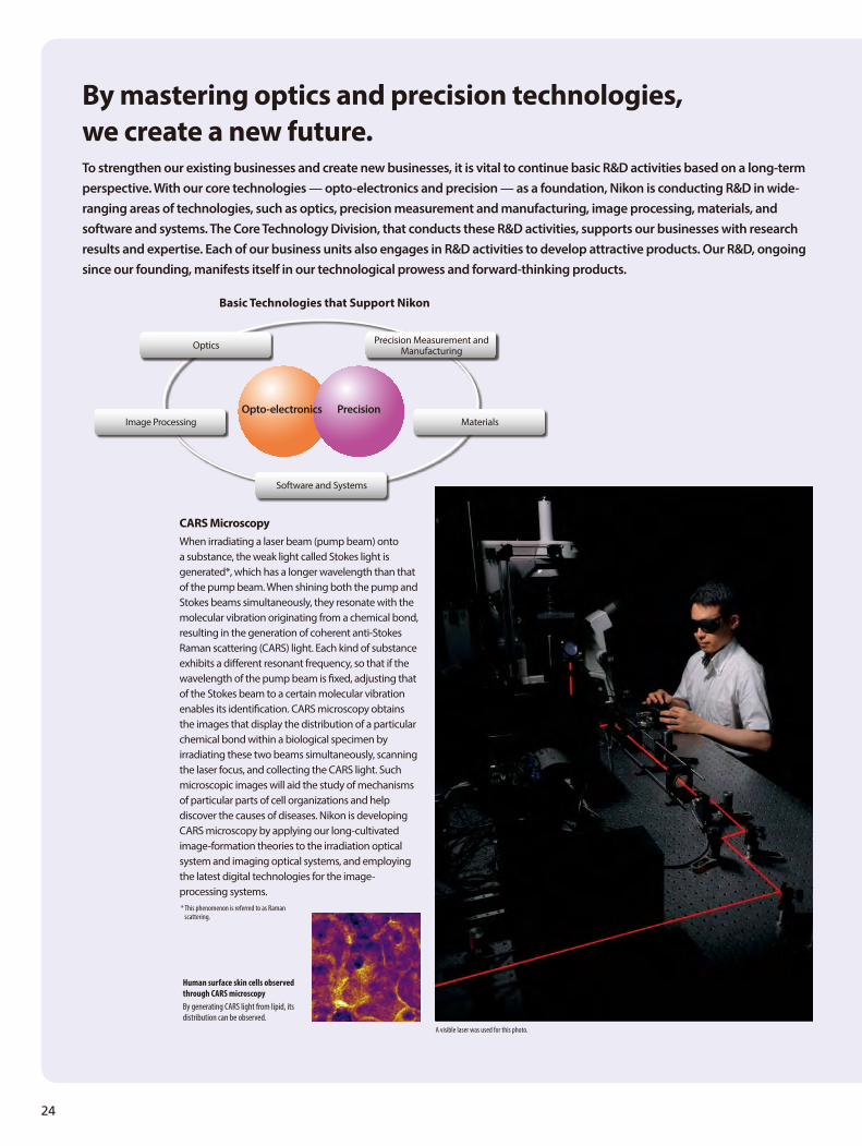
CARS MicroscopyWhen irradiating a laser beam (pump beam) onto a substance, the weak light called Stokes light is generated*, which has a longer wavelength than that of the pump beam. When shining both the pump and Stokes beams simultaneously, they resonate with the molecular vibration originating from a chemical bond, resulting in the generation of coherent anti-Stokes Raman scattering (CARS) light. Each kind of substance exhibits a different resonant frequency, so that if the wavelength of the pump beam is fixed, adjusting that of the Stokes beam to a certain molecular vibration enables its identification. CARS microscopy obtains the images that display the distribution of a particular chemical bond within a biological specimen by irradiating these two beams simultaneously, scanning the laser focus, and collecting the CARS light. Such microscopic images will aid the study of mechanisms of particular parts of cell organizations and help discover the causes of diseases. Nikon is developing CARS microscopy by applying our long-cultivated image-formation theories to the irradiation optical system and imaging optical systems, and employing the latest digital technologies for the image-processing systems.
Human surface skin cells observed through CARS microscopyBy generating CARS light from lipid, its distribution can be observed.
* This phenomenon is referred to as Raman scattering.
A visible laser was used for this photo.
Software and Systems
Image Processing
Optics Precision Measurement and Manufacturing
MaterialsPrecisionOpto-electronics

CNT flexible deviceA semiconductor circuit is fabricated on a plastic substrate with semiconductor CNTs.
Thin Film Transistor Fabrication Technology(Flexible electronics)Thin film transistor fabrication technology of creating electronic circuits or elements on thin, flexible plastic substrates has the potential to revolutionize manufacturing of electronics materials and devices. At Nikon, we conduct R&D of such fabrication technology (flexible electronics). One of our achievements is speedy manufacturing of complex circuits by forming transistors of oxide and organic semiconductors on plastic substrates. By distributing carbon nanotubes (CNT) on plastic substrates, we also developed CNT transistors, which may be applied for driving circuits of liquid crystal displays.
Research and Development
25
Thermal Fluid SimulationIn semiconductor manufacturing, a thin layer of ultrapure water is inserted into a tiny space between the wafer and the projection lens in lithography systems to achieve high resolution. This is known as immersion lithography technology. The latest semiconductor lithography systems require extremely stringent control at the nanometer level. Even the exceedingly small temperature fluctuations in the water affect the accuracy of exposure. Thermal fluid simulation adapting analysis technology predicts and optimizes such temperature fluctuations of ultrapure water, and contributes to improvement of exposure accuracy. One of the aims of analysis technology application is to discern complicated phenomena which occur in product development, and to predict such phenomena with high accuracy. The currently established prediction technology is already utilized for various kinds of product development.
OPTIA, the Metrology System for Interchangeable Camera LensesThe Optical Performance and Total Image Analyzer (OPTIA) is designed to automatically measure and evaluate the optical performance of interchangeable camera lenses. It was based upon wavefront aberration measurement technology that was originally developed for semiconductor lithography systems and has now been optimized for camera lenses. Unlike optical performance measurement categories such as resolution capability and the ability to create contrast which can be expressed numerically, the lens’ ability to create visual appeal does not have established evaluation criteria. At Nikon, we term all such kinds of visual performance as “lens characteristics.” Employing OPTIA, we study the relationship between these lens characteristics and optical performance. In addition, we can produce images that reflect the unique depiction qualities of each lens by using simulation software that was developed simultaneously with OPTIA. Taking advantage of such images allows us to more effectively control optical performance and efficiently develop high-quality lenses that produce attractive images.
Optimizing the ultrapure water temperature in immersion lithography systemsOptimization using thermal fluid simulation has realized uniformity and stability of temperature distribution.
Projection lens
Wafer
Before optimization
After optimization
Ultrapure water

26
Highly Efficient Line ProductionNikon Imaging (China) Co., Ltd. (see photo at right) manufactures products such as compact digital cameras, Nikon 1 Advanced Camera with Interchangeable Lenses, and 1 NIKKOR interchangeable lenses. Nikon (Thailand) Co., Ltd., Nikon’s largest overseas production plant (see photo below), manufactures digital SLR cameras and NIKKOR lenses. At these plants, we use line production based on the pull system; for production of digital SLR cameras, processes from unit assembly to adjustment and inspection are designed to function linearly in an expansive plant. Fast, accurate work creates uniform products of superb quality. We are aggressively advancing efforts to improve each manufacturing process in order to realize further enhanced product quality, optimized work efficiency and shortened work hours.
Precise manufacturing is the thread that connects all Nikon products, from optical components and digital cameras to microscopes and lithography systems. We are working at all our locations around the world to offer high-quality products that meet the needs of society. In addition to introducing the latest manufacturing facilities and technologies, we are shortening manufacturing lead times and reducing costs by reviewing production processes and innovating procurement. In Japan, plants in Oi, Yokohama, Sagamihara, Kumagaya, Mito and Yokosuka, as well as Nikon group companies in other locations, are in charge of production. Our global production system includes overseas facilities such as Nikon (Thailand) Co., Ltd. and Nikon Imaging (China) Co., Ltd.
The joy of turning trust into products.
Manufacturing
27
Cell Production of Digital SLR CamerasSendai Nikon Corporation manufactures our flagship digital SLR cameras. Its cell production realizes higher quality and ensures the timely supply of products. Because each worker is responsible for multiple processes, each must have excellent techniques and uncompromised concentration. Such steady, dedicated effort yields the reliable, world-class products for which Nikon is known.
Manufacture of Synthetic Silica GlassWe use synthetic silica glass for the projection lenses in our semiconductor lithography systems. The glass is formed when oxygen, hydrogen and silicon compound gases react with one another at temperatures reaching 2,000°C (approx. 3,600°F). It takes about a month for us to grow the sediment from the reactions into an ingot that weighs about one ton. Nikon’s Sagamihara Plant produces high-quality synthetic silica glass to support the performance of projection lenses for semiconductor lithography systems.
Adjusting Microscope Objective LensesKurobane Nikon Co., Ltd. produces objective lenses for microscopes. We enhance the optical precision of these lenses by fitting them before the objective lens is completed, then micro-adjusting the lens groups inside the lens barrel while actually looking into the microscope. Then we use a unique inspection system to conduct final aberration checks.
Production of FPD Lithography SystemsFlat panel displays are increasing in size as large-screen LCD TVs and digital signage become more popular. Nikon assembles, adjusts, and inspects FPD lithography systems that can handle extremely large glass plates. We manufacture and ship the stage, optical systems and illumination systems, etc., to our customers as separate units. We then assemble and adjust the components at the customer’s facilities.
Advanced Processing by Nikon Master CraftspersonsWe recognize certain employees as Nikon Master Craftspersons, exceptionally skilled people who take charge of manufacturing the parts of products that require extremely high precision and quality. In the photo at left, a Nikon Master Craftsperson is polishing lenses. Such traditional, sophisticated skills are indispensable when crafting cutting-edge products.

28
Guided by our corporate philosophy, “Trustworthiness and Creativity,” the Nikon Group aims to contribute to the sustainable development of society. As part of such efforts, we established the Nikon CSR Charter, while addressing various issues such as the environment, human rights, and anti-corruption measures throughout our supply chains to show our support for the United Nations Global Compact. Following the launch of the United Nation’s Sustainable Development Goals in 2016, expectations for the private sector to play a greater role in addressing global social issues are increasing. The Nikon Group will continue to proceed with our corporate activities in a sincere manner while maintaining communication with stakeholders, and further enhance our products and services that will lead to solutions of social problems, by utilizing our opto-electronics and precision technologies. It is this process that will help us further contribute to achieving a sustainable society.
Toward a more sustainable world.
Guidelines for Conduct
Our Philosophy
Trustworthiness and Creativity
Customers
Shareholders
Employees
Business Partners
Society
Nikon CSR Charter
Nikon Code of Conduct
Vision
Nikon Group’s basic policy on social responsibility
Our Aspirations
Meeting needs. Exceeding expectations.
Our Commitments
Our vision for the future
The commitments we make on a daily basis in order to achieve our aspirations
Our unending dedication to unchanging principles
Code for daily business activities
Nikon’s Stakeholders

CSR Promotion Organization
Risk Management
Compliance (Corporate Ethics)
Human Rights, Labor Environment and Diversity
CSR Procurement
Aiming to effectively promote CSR, the Nikon Group has established the CSR Committee, a decision-making body for all CSR activities chaired by the Chairman of the Board. In addition, there are two subordinate bodies — the Business Conduct Committee and Environmental Committee, helping CSR to spread and be well-absorbed across the group companies. In the Nikon Group, the ratio of overseas operations is larger than that in Japan, in terms of both net sales and employee numbers, therefore, it is quite important to develop CSR activities at group companies outside Japan. Considering regional characteristics, our three holding companies now have responsibilities for an overall promotional function of CSR activities. In addition, we have divided our global business areas into six regions — Japan, Greater China, Europe, Asia, the Americas, and Korea, and established a CSR Committee in each area for discussing CSR issues.
To supervise risk management, the Nikon Group has created the Risk Management Committee. The Committee identifies risks that might critically impact corporate management, deliberates measures to reduce risks generally and determines in which order risks should be handled. The Nikon Group has also formulated a Business Continuity Plan (BCP). In addition, the Nikon Group takes various measures for information asset management under the instruction of the Information Security Division. We continue to strengthen our risk management system with a wider, holistic view of Nikon Group companies.
The Nikon Group defines compliance as not only complying with laws and regulations but also conducting sound and fair business activities that are in line with corporate rules and social norms. We maintain the established Nikon Code of Conduct, a set of principles for all group companies in Japan and overseas that encourage each employee to become more aware of compliance and able to make the most appropriate judgment in any circumstances. The Nikon Anti-Bribery Guidelines have been formulated to step up our commitments and bolster the Nikon Anti-Bribery Policy of 2014. Regional holding companies took the lead in the development of these guidelines that reflect the actual situation in each region. In order for compliance to fully permeate across the group companies, facilitators at various departments and group companies are working with regional holding companies, conducting relevant activities well established in each locale.
Our fundamental policy is to create an environment where every employee can fully leverage his or her abilities to produce effective results by treating all employees fairly and respecting diversity and human rights. In the year ended March 2015, the Nikon Group established “FUTURE IN FOCUS” as a global human resource measure to help carry out the Medium Term Management Plan “Next 100 — Transform to Grow.” In the year ended March 2016, we began applying this policy to the whole group, launching programs that promote training and effective management of human resources from both a global perspective and across regions and business units. We also held the next-generation leader training program again following its success last year, with selected employees from eight countries attending.
The Nikon Group procures materials from procurement partners in a sincere and fair manner based on the Nikon Basic Procurement Policy. The aim of this policy is to continue providing customers with products that optimally meet their needs, while also helping to create a more desirable society and global environment and realizing the sustainable development of our corporation throughout our supply chains. We have established the Nikon CSR Procurement Standards in order to facilitate the fulfillment of social responsibility, including the prevention of corruption while respecting human rights along the entire length of the supply chain. We also have established Nikon Green Procurement Standards for procuring environmentally friendly parts and materials. In recent years, the Nikon Group has been working, in cooperation with procurement partners, to solve issues of conflict minerals in Africa, as well as to comply with the United Kingdom Modern Slavery Act.
Business Conduct Committee
Environmental Committee
CSR Committee
29
Sustainability
European CSR Committee

Glass Manufacturing Requiring Less Energy
Eco-friendly Products Downsizing Packages
Inverted Microscopes ECLIPSE Ts2 (left) and ECLIPSE Ts2R (right) have been developed for observing cell cultures, etc. in biological and medical research. Employing LED as the light source gives these microscopes the benefits of energy conservation, long battery life and minimized maintenance. They have successfully reduced electricity consumption while in use by approx. 70% compared to previous models.
Nikon Packaging Assessment was established to reduce the environmental impact caused by packaging material. By implementing the rules as early as during package design phases, we are working to create lighter packages, that are easier to recycle and have less environmental impact when discarded, as well as increase the loading capacity of logistics. The photo above shows an example of packaging for a digital SLR camera (D3300), the volume of which was reduced by approx. 35% from the previous model (D3200).
Nikon has invented a new melting technology for optical glass production that requires less energy. By reducing heat loss in a melting furnace and cutting down the number of manufacturing processes, this method emits less CO2 caused by energy use. The photo shows an optical glass production site.
30
Following the Nikon Basic Environmental Management Policy, the Nikon Group is working toward building a sustainable society, emphasizing the realization of a low-carbon society, a resource-circulating society and a healthy and environmentally-safe society as our Long-term Environmental Vision. Our Medium-term Environmental Goals include reducing CO2 emissions by 26% from the fiscal 2013 level across the entire supply chain by 2030, through implementing energy-saving measures, promoting LED lighting, introducing our modal shift initiative and strictly following the energy regulations of each country. Aiming to help realize a resource-circulating society, we will not only consider environmental consequences throughout products life cycle, but also promote the employment of environmentally friendly resources for all corporate activities, make efforts to reduce waste, and reuse resources. Finally, we are determined to contribute to the building of a healthy and environmentally-safe society by protecting the environment from hazardous chemical substances.
Contributing to the establishment of a sustainable society.
Conserving Water Resources
Solar Powered LED Lighting
Solar Power Generation System
Nikon Imaging (China) Co., Ltd. saves approx. 22,800 tons of water every year by reusing concentrated water discharged during processing of RO water (pure water with foreign contaminants removed through Reverse Osmosis).
Nikon Imaging (China) Co., Ltd. replaced the exterior lighting for its premises utilizing LED lights with solar panels. The company is also intending to install LED lights in factory hallways, the transformer substation and compressor rooms, as part of increased efforts to save energy and reduce carbon dioxide emissions.
The Yokohama Plant has a solar power generation system installed on the walls of the building completed in April 2013. It generates approx. 26,000 kWh annually, while slashing carbon dioxide emissions by approx. 10 tons a year. At the Kumagaya Plant, a solar power generation system was launched under a joint research program with the New Energy and Industrial Technology Development Organization (NEDO). It has achieved an annual power generation of more than 100,000 kWh and reduced carbon dioxide emissions by about 50 tons a year.
Yokohama Plant
Kumagaya Plant
31
Environmental Activities

The AKAYA Project for biodiversity restoration is underway at Akaya Forest, a 10,000-hectare government-owned forested area extending into Gunma and Niigata Prefectures in central Japan. Nikon has supported this important project through the cooperation of the Nature Conservation Society of Japan since 2005. Many Nikon products are in use for research and observation: binoculars and Fieldscopes for monitoring birds of prey and cameras for recording purposes. Nikon also provides equipment for an endeavor that aims to enhance the habitat of golden eagles in Akaya, which commenced in September 2014. The plan is intended to restore the forest with rich biodiversity through long-term protection of golden eagles, endangered birds that are often referred to as the barometers of healthy forests. This is the first initiative of its kind in Japan.
The Nikon Group has continued to support recovery efforts following the 2011 Great East Japan Earthquake. Now in its fifth year, a total of 2,432 students from 42 schools and one organization took part in the Photo Book Project for Junior High School Students during the year ended March 2016. Students took photos, selected their favorites, and contributed them to a photo book along with captions expressing their feelings. Nikon meanwhile donated compact digital cameras and provided support through activities such as organizing photography classes at schools. We also continue to operate Nikon Plaza Sendai as a center for reconstruction efforts, while supporting employees who wish to volunteer.
Nikon implements the Nikon Shanti Scholarship, which supports students attending junior high schools, senior high schools and universities in Thailand. These programs were established in 2007 and have assisted approx. 1,500 students. In addition, in 2013, we started sending a framed picture of the scholarship students taken with family and friends as a gift. We hope this offers them a chance to appreciate the joy of photography — the arena in which Nikon excels, while encouraging them in their studies and lives. Also, we established the Nikon-EDF Japan Scholarship for Laos and Nikon-JICA Scholarship for Laos projects in 2014, under which we provide scholarships for approx. 100 junior high school students every year, mainly in Savannakhet Province where Nikon Lao Co., Ltd. is located, and approx. 40 college students at Savannakhet University. Nikon will continue to aid these programs, hoping to support the development of human resources that will play an important role in the future of each country while also cultivating friendship with Japan.
A Nature Conservation Society of Japan’s researcher conducts fixed-point monitoring
Full view of Akaya Forest
Supporting the AKAYA Project in Japan
Assisting Reconstruction in Tohoku
Nikon Scholarship Programs in Thailand and Laos
32
Nikon engages in community contribution activities in all countries and regions where we operate, in the following five areas: environment, education, social welfare, culture and arts, as well as assistance for reconstruction. As a responsible corporate citizen, we are seeking to grow together with the community, and to contribute to society’s sound, sustainable development. Each and every employee of the Nikon Group endeavors to maintain awareness as a good citizen at all times, while participating in activities beneficial for the community as appropriate.
Supporting communities — Nikon’s social and cultural activities.

33
Social Contribution and Cultural Activities
Opened in October 2015, the Nikon Museum showcases some 600 items from consumer products such as cameras and binoculars to industrial equipment including semiconductor lithography systems, displayed in its 600 m2 space. The facility allows visitors to learn about the history of each business, as well as Nikon products and technologies, etc.
In 1968, we opened a photo gallery in Ginza called Nikon Salon. Today, Nikon Salons in Ginza, Shinjuku and Osaka display the works of professional and amateur photographers from around the world, chosen through a stringent selection process by an independent panel. Each year, Nikon Salon presents awards to outstanding photographers, including the Ina Nobuo Award, the Miki Jun Award and the Miki Jun Inspiration Award.
The Nikon Chair of Imaging Science was established in April 2012 as the successor to the Nikon Chair of Optical Engineering, which had operated at the University of Tokyo’s Institute of Industrial Science since November 2006 to develop Japan’s next generation of optical industry leaders. The Chair offers lessons in fundamentals such as geometric optics, wave optics, image-processing technology and practical lens design. It also increases opportunities for industrial-academic cooperation between promising optics researchers and engineers, furthering their ability to compete at a world-class level.
The Nikon Photo Contest has become one of the world's largest global photo contests since it was first held in 1969. It provides a great opportunity for photographers, both professionals and amateurs, to communicate and enrich photographic culture. Commemorating Nikon’s celebration of its 100th anniversary in 2017, we newly established the Nikon 100th Anniversary Award as well as the Next Generation Award to recognize young talent, looking ahead to the future of image culture.
New logo designed by Neville Brody, the internationally renowned art director serving as Lead Judge of the Contest
Nikon Museum
Nikon Salons
Nikon Chair of Imaging Science at the University of Tokyo
Nikon Photo Contest
Neville Brody

34
Nikon’s corporate history began in 1917 and the manufacture of optical glass started the next year. Since then, the two constants have always been our awareness of users’ stringent demands and our uncompromising attitude toward manufacturing to continuously meet those demands. This spirit has uninterruptedly been handed down in Nikon.
Mastering optical and precision technologies.
1917
●Three of Japan’s leading optical manufacturers merge to form a comprehensive, fully integrated optical company known as Nippon Kogaku K.K.
1918
●Oi Dai-ichi Plant (now Oi Plant) is completed
1952
●nikkor club is established to promote photography culture
1953
●Nikon Optical Co., Inc. [now Nippon Kogaku (U.S.A.) Inc.] is established to export Nikon cameras to the U.S. and conduct technical services and market research
1959
●Nikon F, Nikon’s first SLR camera, is marketed
1932
●NIKKOR is adopted as the brand name for camera lenses
1945
●With the end of World War II, production shifts to cameras, microscopes, binoculars, surveying instruments, measuring instruments and ophthalmic lenses, etc.
1946
●Pointal ophthalmic lens is marketed
●Nikon brand name is adopted for small-sized cameras
1947
●Tilting Level E and Transit G surveying instruments are marketed
1948
●Nikon Model I small-sized camera is marketed
●Model I profile projector is marketed
1967
●Oi Plant’s Ofuna site (now Yokohama Plant) is built
1968
●Photo gallery Ginza Nikon Salon is opened
●Nikon Europe N.V. (now Nikon Europe B.V.) is established in the Netherlands
1921
●MIKRON 4x, 6x ultra-small-prism binoculars are marketed
1925
●JOICO microscope is marketed
1910 1920 1930 1940 1950 1960
Nikon Model I
Nikon F
Nikon at the time of founding
JOICO microscope

35
Corporate History
1971
●Nikon Photomic FTN is mounted on Apollo 15
●Oi Plant’s Sagamihara site (now Sagamihara Plant) is built
1990
●Nikon (Thailand) Co., Ltd. is established
1991
●Mito Plant is built
1992
●Nikon Instech Co., Ltd. is established
1995
●Nikon Singapore Pte. Ltd. is established
1999
●D1 digital SLR camera is marketed
●In-house company system is inaugurated
1980
●Nikon F3 SLR camera is marketed
●NSR-1010G Step-and-Repeat System is marketed
1981
●Ehrenreich Photo-Optical Industries, Inc. is acquired in the U.S. and renamed Nikon Inc.
●Nikon Fieldscope is marketed
1984
●Kumagaya Plant is built
1985
●Total Station DTM-1 surveying instrument is marketed
1986
●NSR-L7501G large substrate exposure system is marketed
1988
●Nikon Photo Products Inc. (now Nikon Imaging Japan Inc.) is established
●Corporate name is changed to Nikon Corporation
2000
●Nikon-Essilor Co., Ltd., joint venture with Essilor International of France, is established
2002
●Nikon Imaging (China) Co., Ltd. is established
2003
●Nikon-Trimble Co., Ltd., a joint venture with Trimble Navigation Ltd. of the U.S., is established
2004
●Yokohama Plant’s Yokosuka Branch (now Yokosuka Plant) is built
●Nikon F6 SLR camera is marketed
2005
●Nikon Imaging (China) Sales Co., Ltd. begins operations
2006
●NSR-S609B ArF immersion scanner is marketed
2007
●D3 digital SLR camera is marketed
2009
●FX-101S FPD Scanner is marketed
●Metris NV became Nikon Metrology NV, a wholly owned subsidiary of Nikon Corporation
1970 1980 1990 2000 2010
FX-101S
First overseas production facility Nikon (Thailand) Co., Ltd.
NSR-1010G
2010
●D3S and D3X digital SLR cameras, and NIKKOR lenses, are used in the International Space Station (ISS)
2011
●Nikon 1 J1 and V1 advanced cameras with interchangeable lenses are marketed
2012
●Nikon Plaza Sendai is opened
●D4 digital SLR camera is marketed
2013
●Nikon Lao Co., Ltd. is established in Laos
2014
●Head office is relocated to Tokyo’s Shinagawa area (Shinagawa Intercity Tower C, 2-15-3, Konan, Minato-ku, Tokyo)
2015
●Optos Plc became a wholly owned subsidiary of Nikon Corporation●The Nikon Museum is opened
2016
●NSR-S631E ArF immersion scanner is marketed●D5 digital SLR camera is marketed
Nikon 1 V1
NSR-L7501G
Nikon D5

Company Profile 2016
This eco-friendly booklet was produced using FSC®-certified paper; non-VOC (volatile organic compound), vegetable-oil ink; and waterless printing technology.Shinagawa Intercity Tower C, 2-15-3, Konan, Minato-ku, Tokyo 108-6290 Japan
2016.9