Common-Source Amplifier Stage -...
18
45 5 Common-Source Amplifier Stage Two types of common-source amplifiers will be investigated in lab projects. One is with the source grounded and the other is with a current-source bias (dual power supply). In Units 5.1 and 5.2 we discuss various aspects of the common-source stage with grounded source, in Unit 5.3 we take up circuit-linearity considerations, and in Unit 5.4 we cover the basics of the dual-power-supply amplifier. Both amplifiers are based on the PMOS, as in the projects. The first two units are mostly a review of the basic amplifier as presented in previous units, to reinforce the basic concepts. The PMOS replaces the NMOS (Units 2 and 4) in this unit, to provide familiarity with the opposite polarity in bias considerations and to illustrate that the linear model applies in the same manner for both transistor types. 5.1 DC (Bias) Circuit Dc circuits for the grounded-source amplifier are shown in Fig. 5.1 (PMOS). The circuit in (a) is based on a single power supply, and the gate bias is obtained with a resistor voltage-divider network. The circuit in (b) is for a laboratory project amplifier. Both and are negative, since the source is at ground. There is no voltage drop across since there is negligible gate current. is necessary only to prevent shorting the input signal, . The bias current for a given applied will respond according to (3.8), which is ( )( ) λ + − = 1 2
Transcript of Common-Source Amplifier Stage -...

45
5555
Common-Source Amplifier Stage
Two types of common-source amplifiers will be investigated in lab projects. One is with the source grounded and the other is with a current-source bias (dual power supply). In Units 5.1 and 5.2 we discuss various aspects of the common-source stage with grounded source, in Unit 5.3 we take up circuit-linearity considerations, and in Unit 5.4 we cover the basics of the dual-power-supply amplifier. Both amplifiers are based on the PMOS, as in the projects. The first two units are mostly a review of the basic amplifier as presented in previous units, to reinforce the basic concepts. The PMOS replaces the NMOS (Units 2 and 4) in this unit, to provide familiarity with the opposite polarity in bias considerations and to illustrate that the linear model applies in the same manner for both transistor types.
5.1 DC (Bias) Circuit Dc circuits for the grounded-source amplifier are shown in Fig. 5.1 (PMOS). The circuit in (a) is based on a single power supply, and the gate bias is obtained with a resistor voltage-divider network. The circuit in (b) is for a laboratory project amplifier. Both GGV and SSV are negative, since the source is at ground. There is no voltage drop across GR since there is negligible gate current. GR is necessary only to prevent shorting the input signal, iV . The bias current DI for a given applied SGV will respond according to (3.8), which is
( ) ( )SDptpoSGpD VVVkI λ+−= 12
Prentice Hall PTR
This is a sample chapter of Analog Electronics with LabVIEW ISBN: 0-13-047065-1 For the full text, visit http://www.phptr.com ©2002 Pearson Education. All Rights Reserved.

46 Unit 5 Common-Source Amplifier Stage
Fig. 5.1 Basic PMOS common-source amplifiers. Single-power-supply amplifier (a) and laboratory amplifier (b) with SG GGV ( V )= and SSV controlled by DAQ output
channels. Note that either end of the circuit of (a) can be at ground.
DR
SSV
2GR
iV
oV
1GR
)a(
DR
SSV
GR
iV
oV
GGV
)b(
The two circuits are equivalent, as GGV and GR of Fig. 5.1.b are the Thévenin equivalent of the bias network of the Fig. 5.1(a). In the project on the amplifier, they are actually a voltage and a resistor. This is not a bias-stable circuit, as a slight change in SGV or the transistor parameters can result in a significant change in DI . The dual-power-supply circuit of Unit 5.4 is considerably better in this respect.
5.2 Amplifier Voltage Gain This dc (bias) circuit becomes an amplifier now simply by adding a signal source at the gate as in Fig. 5.2. This requires a coupling capacitor, as shown here in the complete circuit, to prevent disturbing the bias upon connecting the input signal to the circuit.
In the amplifier of Project 5, the signal will be superimposed on the bias voltage at the node of GGV . This can be facilitated with LabVIEW and the DAQ. A capacitor, as in an actual amplifier, is therefore not required. The requirement for having LabVIEW control over both GGV and SSV , and the limitation of two output channels, dictates this configuration.
In Project 5 we measure the gain as a function of bias current, DI . For a SPICE comparison, we need an expression for the gain. For the ideal case, which neglects the output conductance, dsg , the output current is related to the input voltage by (4.1), which is
imgsmd VgVgI ==

Unit 5.2 Amplifier Voltage Gain 47
Fig. 5.2 A signal source is connected to the gate through a coupling capacitor. The capacitor is necessary to isolate the dc circuit from the signal source.
DR
GGV
SSV
GR
iV
oV
sV gC−+
The output signal voltage is, in general,
Ddods RIVV −== (5.1)
+
-Vgs
iV
oV
gsmVgD
R
GR
Fig. 5.3 Signal-equivalent version of the amplifier stage. Dc nodes are set to zero volts (circuit reference). The reactance of gC is assumed to be zero.
The convention used here for subscript order for signal (linear) variables is common to the NMOS and PMOS. This is consistent with the fact that the linear model does not distinguish between the two types. Thus, for example, the dc terminal voltage for a PMOS is SGV , but the signal equivalent is gsV (Fig. 5.3) and the signal input voltage is positive at the input terminal (common-source, gate input). For the PMOS, Di is defined as positive out of the drain, but the signal output current is into the drain (as in the NMOS). We note that a positive gsV ( sggs VV −= ) corresponds to a decrease in the total gate – source voltage, SGv , which is consistent with a decrease of Di and positive dI .

48 Unit 5 Common-Source Amplifier Stage
Thus, the negative sign in (5.1) is consistent with the flow of current dI up through the resistor (Fig. 5.3) for positive i gsV V= . The common-source stage is an
inverting amplifier and has an inherent o180 phase shift. From (4.1) and (5.1), the gain is
Dmi
ov Rg
V
Va −== (5.2)
where both i gsV V= and o dsV V= are with respect to ground or the source terminal for the common-source stage.
If the output resistance, ds1 / g , cannot be neglected (which is the case for the project on PMOS amplifiers), the transistor current, m ig V, is shared between the output resistance and DR . The portion that flows through DR is (Fig. 5.4)
DdsimR
Rg1
1VgI
D += (5.3)
Note again that the signal schematic transistor represents a current source with value imVg , as established in connection with Fig. 4.1. The additional feature of the transistor model is included with the addition of
ds1/g . This resistance is
actually part of the transistor and is between the drain and source of the transistor, but the circuit as given is equivalent, as the source is at ground. Since the output voltage is DRo RIV
D−= , the new gain result is
Dsd
Dmv
Rg1
Rga
+−= (5.4)
Note that this form evolves from ideal transistor current, m gsg V , flowing through the parallel combination of the output resistance and DR .
To facilitate an intuitive grasp of the magnitude of the effect of dsg , we use the expression for dsg (4.13) in (5.4), to obtain
DDp
Dmv
RI1
Rga
λ+−= (5.5)
Note that DDRI is the voltage drop across DR . For example, for a 10-V− power supply, we choose D DI R 5 V≈ . A measurement of pλ for our devices will show that

Unit 5.2 Amplifier Voltage Gain 49
p 1 / 20 V,λ ≈ which results in p D DI R 1 / 4λ ≈ . Thus, the effect of )I(g Dpds λ= for this case is significant.
iV
oV
imVg
DR
GR
dsg/1
Fig. 5.4 Common-source amplifier stage signal circuit, with all dc nodes set to zero volts. The transistor model includes output resistance ds1/g , which appears directly in parallel with DR with the source grounded.
Finally, we can get an overall current dependence for
va with the elimination
of m
g , using (4.5) with p p
k k′ ≈ , which results in
DDp
DDpv
RI1
RIk2a
λ+−= (5.6)
Using an alternative form for )V/I2(g effpDm = , also (4.5), the gain expression is
DDp
D
effp
Dv
RI1
R
V
I2a
λ+−= (5.7)
where
D Deffp
p p SD p
I IV
k (1 V ) k= ≈
+ λ
For simplicity, approximate forms of (4.5) and (4.13) of mg and dsg are used here, which are independent of SDV . For reference, the “exact” and approximate forms of (4.5) and (4.13), respectively, are repeated here:
m p p SD D p Dg 2 k (1 V )I 2 k I= + λ ≈ and

50 Unit 5 Common-Source Amplifier Stage
DpSDp
Dpds I
V1
Ig λ≈
λ+λ=
The “exact” equations of mg and dsg are used in conjunction with the amplifier projects to compare the computed gain with the measured gain plotted against DI . This is done in both LabVIEW and Mathcad. Parameters pk and tpoV (to get
effpV ) will be extracted from the measured dc data, and pλ will be used as an adjustable parameter to fit the SPICE and measured gain data.
5.3 Linearity of the Gain of the Common-Source Amplifier
The connection between dI and gsV is linear provided that gsV is small enough, as considered in the following units. Use of the linear relations also assumes that the output signal remains in the active region (i.e., neither in the linear region nor near cutoff). This is discussed below. NMOS subscripts are used. The results are the same for the PMOS, with a “p ” subscript substituted for “n ” and the subscript order reversed for all bias-voltage variables.
5.3.1 Nonlinearity Referred to the Input The general equation again is (3.8)
( )2tnoGSnD
Vvki −′= Then using DDd IiI −= and GS GS gsv V V= + , the equation for the incremental drain current becomes
( ) 2d n GS tno gs gsI k 2 V V V V ′= − + (5.8)
which leads to a nonlinear (variable) transconductance, mg′ , given by
( )2n effn gs gs gsd
m mgs gs effn
k 2V V V VIg g 1
V V 2V
′ + ′ = = = ±
(5.9)
Therefore, the condition for linearity is that effgs V2V << , with tnoGSeffn VVV −=

Unit 5.3 Linearity of the Gain of the Common -Source Amplifier 51 and using m n effng 2k V′= .
With this condition not satisfied, an output signal is distorted. However, for the purpose of measuring the amplifier gain, our signal voltmeter will take the average of the positive and negative peaks, which is
( ) ( )2
VVV2kVVV2kI
2gsgseffn
2gsgseffn
davg
−′++′= (5.10)
In the parabolic relationship, the squared terms cancel entirely. In general, though, the output signal contains harmonic content (distortion) when gsV is too large compared to effnV .
5.3.2 Nonlinearity Referred to the Output The discussion above of limits imposed on gsV assumes that the transistor remains in the active mode. To clarify this point, reference is made to the output characteristics of Fig. 5.5. The graph has plots of the output characteristic for three values of GSv in addition to the load line. The characteristic plot in the midrange is for no signal. Operating point variables are DSV 2.5 V≈ and DI 40 A≈ µ . With a large, positive gsV , the characteristic moves up to the high-level
plot ( Dhii ) and the opposite occurs for a large but negative gsV ( Dloi ). The high-level plot is shown for when the transistor is about to move out of the active region and into the linear region. Attempts to force DSv to lower values will create considerable distortion in the output signal voltage. The lower curve suggests that the positive output signal is on the verge of being cut off (clipped) for an additional increase in the negative-input signal voltage.
According to the discussion above, the negative signal output voltage is limited to
effnDSminusds VVV −= (5.11) Technically, effnV is from the high-current signal state, but for simplicity, a reasonable estimate can be made from the dc case; that is, effn GS tnoV V V= − . The positive signal limit is
DDDSDDplusds RIVVV =−= (5.12

52 Unit 5 Common-Source Amplifier Stage
)A(iD µ
)V(vDS
DSV
DI
Dhii
Dloi
effnv
Fig. 5.5 Common-source amplifier stage output characteristics. Output characteristics are from top to bottom, large high-current signal swing, Dhii , dc bias, DI , low-current signal swing,
Dloi . Also shown is the load line.
The current – voltage circuit solution is always the intersection between a given characteristic and the load line.
The actual output-signal limit is dictated by the smaller of the two for a symmetrical periodic signal such as a sine-wave. In the example shown in Fig. 5.5, effnV 0.5 V≈ , DSV 2.5 V≈ , and DDV 5 V= . The plus and minus signal-voltage limits are about V5.2 and 2.0 V, respectively. Depending on the dc bias, the limit could be dictated by one or the other. In the amplifier projects, the gain will typically be measured over a range of dc bias current for a fixed resistor. This means that for the low-current end of the scan, the signal will be limited by the magnitude of DDRI and, by design, the plus and minus swings will be made to be about equal at the highest dc current.
Distortion associated with the nonlinear dI – gsV relation and that due to signal limits at the output may be taking place simultaneously. This is seen from the gain expression (5.7) )0g( ds =
DR
veffp
Va 2
V≈
where gsdsv V/Va ≡ and where the approximation is for the case of neglecting the
nλ factor. Thus, for a given dsV , gsV is
Unit 5.4 Current-Source Common-Source Amplifier: Common-Source Amplifier with a Source Resistor 53
dsR
effpgs V
V2
VV
D
= (5.13)
If, for example, dsV is pushed to the positive output-signal limit, then
Dds RV V≈ .
According to (5.13), gs effpV V / 2= , and gsV exceeds the condition for a linear dI –
gsV relation as given in (5.9),
gsdm m
gs effn
VIg g 1
V 2V
′ = = ±
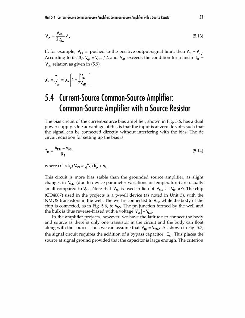
5.4 Current-Source Common-Source Amplifier: Common-Source Amplifier with a Source Resistor
The bias circuit of the current-source bias amplifier, shown in Fig. 5.6, has a dual power supply. One advantage of this is that the input is at zero dc volts such that the signal can be connected directly without interfering with the bias. The dc circuit equation for setting up the bias is
S
SGDDD
R
VVI
−= (5.14)
where ( p pk k′ ≈ ) SG D p tpV I / k V≈ + . This circuit is more bias stable than the grounded source amplifier, as slight changes in SGV (due to device parameter variations or temperature) are usually small compared to DDV . Note that tpV is used in lieu of tpoV as BSV 0≠ . The chip (CD4007) used in the projects is a p-well device (as noted in Unit 3), with the NMOS transistors in the well. The well is connected to SSV , while the body of the chip is connected, as in Fig. 5.6, to DDV . The pn junction formed by the well and the bulk is thus reverse-biased with a voltage SS DDV V+ .
In the amplifier projects, however, we have the latitude to connect the body and source as there is only one transistor in the circuit and the body can float along with the source. Thus we can assume that .VV tpotp = As shown in Fig. 5.7, the signal circuit requires the addition of a bypass capacitor, sC . This places the source at signal ground provided that the capacitor is large enough. The criterion

54 Unit 5 Common-Source Amplifier Stage
for this is discussed in Unit 6. The voltage-gain equation is the same as in the amplifier, with the source actually grounded.
Fig. 5.6 Dc circuit of the dual-power-supply common-source amplifier. The gate is at ground potential, allowing the signal to be connected directly to the gate. GR is necessary only to prevent shorting out the input signal.
DR
SR
DDV
SSV
GR
−
+
SGV
DV
DDV
Without the bypass capacitor, SR is in the signal circuit and a fraction of the
applied signal voltage at the gate is dropped across the resistor. The signal circuit for this case is shown in Fig. 5.8. The circuit transconductance of the amplifier with SR was discussed initially in Unit 4. This is reviewed in the following.
Fig. 5.7 Amplifier circuit with a bypass capacitor attached between the source and ground to tie the source to signal ground. Signal input is attached directly to the gate. Body and source are connected internally in the project chip for the transistor used in the amplifier.
DDV
sC
SR
DR
GRoVgi VV =
−+
SSV
An applied input signal, i gV V= , divides between the gate – source terminals
and the source resistor according to [(4.6)]
Sdgsg RIVV +=

Unit 5.5 Design of a Basic Common-Source Amplifier 55
Fig. 5.8 Signal circuit for dual-power supply common-source amplifier. Input signal voltage,
iV, is divided between gsV ,
the control voltage, and the source resistor according to the ratio m S1 : g R .
SR
DR
GR oVgi VV =
+
-Vgs
−+
When combing this with gsmd VgI = , we obtain [(4.7)]
( ) ( ) dg gs m gs S m S gs m S
m
IV V g V R 1 g R V 1 g R
g= + = + = +
The circuit transconductance, mG , is then [(4.8)]
Sm
m
g
dm
Rg1
g
V
IG
+==
The gain for this case is thus (neglecting dsg )
Sm
DmDm
g
dv
Rg1
RgRG
V
Va
+−=−== (5.15)
In one of the amplifier projects, DS RR = , and the gain without the bypass capacitor is actually less than unity.
5.5 Design of a Basic Common-Source Amplifier Unlike in the laboratory environment, an actual practical common-source amplifier would have a single power supply for the base and collector circuit bias. Also, the circuit design requires a tolerance to a wide range of parameter

56 Unit 5 Common-Source Amplifier Stage
variation, including that due to temperature change. In this unit, the design process for a possible common-source amplifier is discussed. Emphasis is on dc bias stability, that is, on tolerance to device parameter and circuit component variations.
The common-source amplifier to be designed is shown in Fig. 5.9. Source resistor,
SR , is included for bias (and gain) stabilization. The goal is for the circuit
to function properly for any NMOS transistor, which has device parameters nk and
tnoV that fall into a wide range of values, as is normally expected. Tolerance
to component variation, such as resistor values, could also be built into the design.
Fig. 5.9 NMOS common-source amplifier with
SR for bias and gain stabilization. Gate
bias is provided by a voltage-divider network consisting of
G1R and
G2R . The body
and source terminals are connected.
DR
SR2GR
DDV
sC
oVgC
iV
1GR
Gate voltage GV is provided by the voltage divider, consisting of resistors 1GR
and G2R . Since there is no gate current, the gate bias voltage is [(1.2)]
DD1G2G
2GG V
RR
RV
+=
Voltage GV is thus relatively stable and can be considered constant. Once GV has been established, the drain current will be dictated by
S
GSGD
R
VVI
−= (5.16)
Since the gate – source voltage is given by

Unit 5.5 Design of a Basic Common-Source Amplifier 57
tnon
DGS V
k
IV += (5.17)
the drain current, DI , may be expressed in terms of the device parameters as
S
tnon
DG
DR
Vk
IV
I
−−= (5.18)
This result reveals the dependence of DI on the magnitudes of nk and tnoV . (Again, for simplicity, as in the amplifier projects, we will assume that the body and source are connected such that tn tnoV V= .)
Bias current DI is assumed to be a given. The initial design then is conducted for the NMOS nominal, average values for nk and tnoV . Any combination of GV and SR that satisfies (5.18) will provide the design DI . Specific values for GV and
SR will be dictated by stability requirements. Suppose that nk is expected to fall within no nk k± δ and tnoV within tnoo tnoV V± δ , where nok and tnooV are the nominal values of the original design. Assume that the design bias current associated with nok and tnooV is DoI . At the extremes for the parameters, the low and high currents
will be
( )DG tnoo tno
no nDlo,Dhi
S
IV V V
k kI
R
− − ± δδ
=∓
(5.19)
Resistor
SR , for the given GV and design drain current, is
Do
GSoGS
I
VVR
−= (5.20)
GSoV is obtained from (5.17), using the nominal parameter values. The low and
high current limits tend to converge on G S
V /R as GV becomes large. That is, in the limit, GV dominates the voltages in the numerator of (5.19), thus rendering the expression insensitive to the minor contributions from changes in nk and
tnoV .
An important design consideration is drain – source voltage, DSV , as this
dictates the output signal range. This is calculated from

58 Unit 5 Common-Source Amplifier Stage
( )SDDDDDS RRIVV +−= (5.21)
In the design of the amplifier, drain resistor
DR is normally selected for equal
positive and negative peak-signal maximums. This configuration is illustrated in Fig. 5.10, which shows the output characteristic of the transistor in the circuit. The signal is limited by
SRDD VV − and tnoGSoeffno VVV −= at the high and low ends of the voltage range, respectively. Therefore, nominal bias should be set at
2
VRIVV
effnoSDoDD
DSo
+−= (5.22)
For simplicity, it is assumed that
effn effnov V≈ .
effnoV ,
DDoV , and DoI are the bias
values at the nominal parameter values. The bias drain voltage is DSoV plus the drop across
SR , that is,
SDoDSoDo RIVV += (5.23)
Knowing DoV then provides for the calculation of DR from
Do
DoDD
DI
VVR
−= (5.24)
where DoV and DoI are for the initial design with nok and
tnooV .
An optimization design sequence plots the limits for a range of GV and for specified tnoVδ and
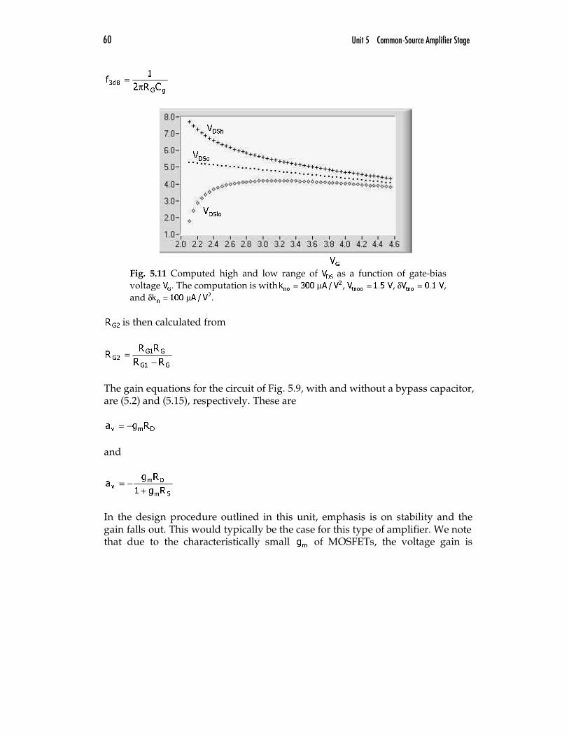
nkδ . An example is shown in Fig. 5.11. The plot of DSoV
corresponds to the nominal nok and tnoo
V . The curve slopes downward as SDRI increases for increasing GV at constant nominal bias current,
DoI . DShiV is for the
combination of tnoVδ and n
kδ , which gives the maximum positive deviation from the nominal, and DSloV is the opposite. The example of Fig. 5.11 is for V10VDD = and design bias current of A100IDo µ= and nominal parameters 2
nok 300 A / V= µ ,
tnooV 1.5 V= ,
tnoV 0.1 Vδ = , and 2
nk 100 A / Vδ = µ . Experience with the CMOS chip of
our amplifier project (Project 7) indicates that these are representative. Figure 5.12 shows plots of the computed positive and negative signal-peak
limits. Due to the increasing S
RV with increasing
GV , the signal range decreases, as
shown by the plots. Thus, the signal-peak limits have a maximum, as is evident in the graph. The design of the amplifier uses
GV at the maximum of the lower

Unit 5.5 Design of a Basic Common-Source Amplifier 59 curve. The value of GV is consistent with the maximum DSloV in the plot of Fig. 5.11. In the example,
GV 3 V≈ .
)A(iD µ
)V(vDS
DSV
DI
DsigiDR
i
effnv
SD RRi +
SDDD RIV −
Fig. 5.10 Output characteristic of the transistor of the amplifier with bias DSV set approximately according to (5.22). The signal is restricted within the range
SRDD VV − and approximately effnv . The characteristic
curves are for no signal (solid plot) and for the signal at a maximum (dashed plot), as limited by the transistor going into the inactive (linear) region. The load lines are dc (solid line) and signal (ac, dashed line).
Once GV is determined, the selection of 1GR is made from (1.2), which is
DD1G
GDD
1G2G
2GG V
R
RV
RR
RV =
+=
where GR is the parallel combination
1G2G
1G2GG
RR
RRR
+=
GR can be selected somewhat arbitrarily but could be dictated by the coupling
capacitor, gC , requirement. Associated with the coupling capacitor is the dB-3 frequency (6.2), which is
60 Unit 5 Common-Source Amplifier Stage
gGdB3
CR2
1f
π=
DShiV
DSloV
DSoV
GV Fig. 5.11 Computed high and low range of
DSV as a function of gate-bias
voltage G
V . The computation is with 2
nok 300 A / V= µ ,
tnooV 1.5 V= ,
tnoV 0.1 Vδ = ,
and 2
nk 100 A / Vδ = µ .
2GR is then calculated from
G1G
G1G
2GRR
RRR
−=
The gain equations for the circuit of Fig. 5.9, with and without a bypass capacitor, are (5.2) and (5.15), respectively. These are
Dmv Rga −= and
Sm
Dm
vRg1
Rga
+−=
In the design procedure outlined in this unit, emphasis is on stability and the gain falls out. This would typically be the case for this type of amplifier. We note that due to the characteristically small mg of MOSFETs, the voltage gain is

Unit 5.5 Design of a Basic Common-Source Amplifier 61 relatively small. Gain can be improved considerably through the use a current-source load, as in the amplifier of Unit 10.
usmindV
dplusV
GV
dplusV
dminusV
Fig. 5.12 Computed maximums for negative and positive output voltage signal peaks as a function of
GV : dplusV , positive maximum; dminusV , negative
maximum.
62 Unit 5 Common-Source Amplifier Stage
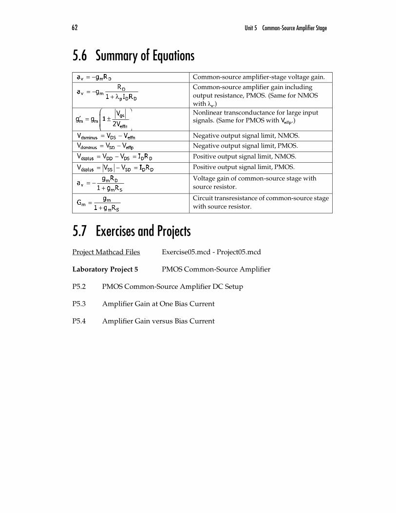
5.6 Summary of Equations
Dmv Rga −= Common-source amplifier-stage voltage gain.
DDp
Dmv
RI1
Rga
λ+−=
Common-source amplifier gain including output resistance, PMOS. (Same for NMOS with nλ .)
gs
m meffn
Vg g 1
2V
′ = ±
Nonlinear transconductance for large input signals. (Same for PMOS with effpV .)
effnDSminusds VVV −= Negative output signal limit, NMOS.
effpSDminusds VVV −= Negative output signal limit, PMOS.
DDDSDDplusds RIVVV =−= Positive output signal limit, NMOS.
DDSDSSplusds RIVVV =−= Positive output signal limit, PMOS.
Sm
Dmv
Rg1
Rga
+−=
Voltage gain of common-source stage with source resistor.
Sm
mm
Rg1
gG
+=
Circuit transresistance of common-source stage with source resistor.
5.7 Exercises and Projects Project Mathcad Files Exercise05.mcd - Project05.mcd Laboratory Project 5 PMOS Common-Source Amplifier P5.2 PMOS Common-Source Amplifier DC Setup P5.3 Amplifier Gain at One Bias Current P5.4 Amplifier Gain versus Bias Current