COMBINATIONAL LOGIC - University of California, … · Dynamic CMOS Logic Domino ... Digital...
73
Digital Integrated Circuits © Prentice Hall 1995 Combinational Combinational Logic Logic COMBINATIONAL LOGIC
Transcript of COMBINATIONAL LOGIC - University of California, … · Dynamic CMOS Logic Domino ... Digital...
Digital Integrated Circuits © Prentice Hall 1995Combinational Combinational LogicLogic
COMBINATIONALLOGIC
Digital Integrated Circuits © Prentice Hall 1995Combinational Combinational LogicLogic
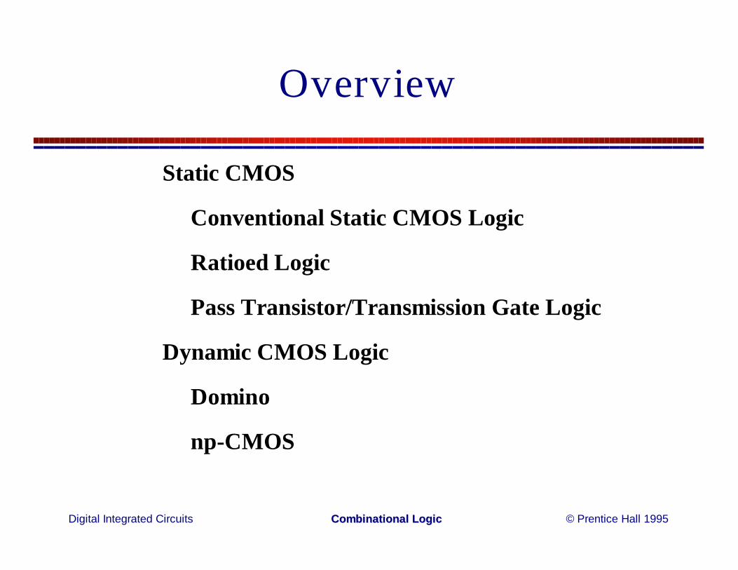
Overview
Static CMOS
Conventional Static CMOS Logic
Ratioed Logic
Pass Transistor/Transmission Gate Logic
Dynamic CMOS Logic
Domino
np-CMOS
Digital Integrated Circuits © Prentice Hall 1995Combinational Combinational LogicLogic
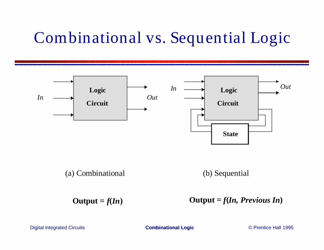
Combinational vs. Sequential Logic
Logic
Circuit
Logic
CircuitOut
OutInIn
(a) Combinational (b) Sequential
State
Output = f(In) Output = f(In, Previous In)
Digital Integrated Circuits © Prentice Hall 1995Combinational Combinational LogicLogic
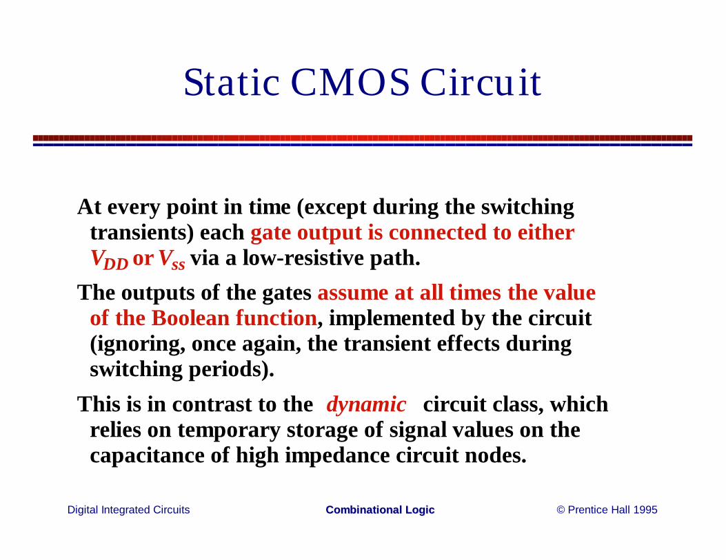
Static CMOS Circuit
At every point in time (except during the switching transients) each gate output is connected to either VDD or Vss via a low-resistive path.
The outputs of the gates assume at all times the value of the Boolean function, implemented by the circuit (ignoring, once again, the transient effects during switching periods).
This is in contrast to the dynamic circuit class, which relies on temporary storage of signal values on the capacitance of high impedance circuit nodes.
Digital Integrated Circuits © Prentice Hall 1995Combinational Combinational LogicLogic
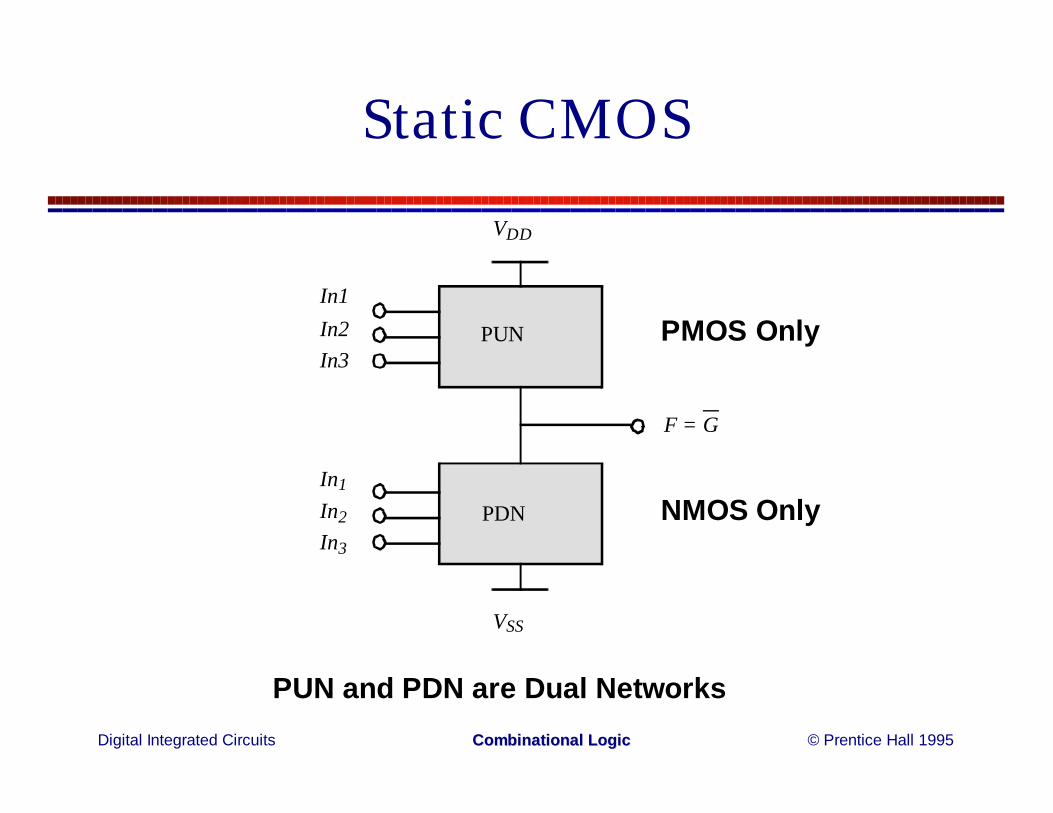
Static CMOSVDD
VSS
PUN
PDN
In1In2In3
F = G
In1
In2
In3
PUN and PDN are Dual Networks
PMOS Only
NMOS Only
Digital Integrated Circuits © Prentice Hall 1995Combinational Combinational LogicLogic
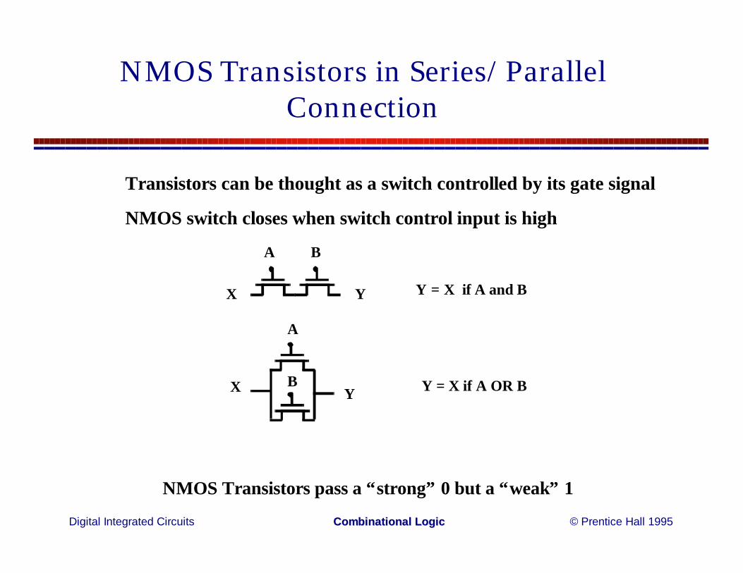
NMOS Transistors in Series/ParallelConnection
Transistors can be thought as a switch controlled by its gate signal
NMOS switch closes when switch control input is high
X Y
A B
Y = X if A and B
X Y
A
B Y = X if A OR B
NMOS Transistors pass a “strong” 0 but a “weak” 1
Digital Integrated Circuits © Prentice Hall 1995Combinational Combinational LogicLogic
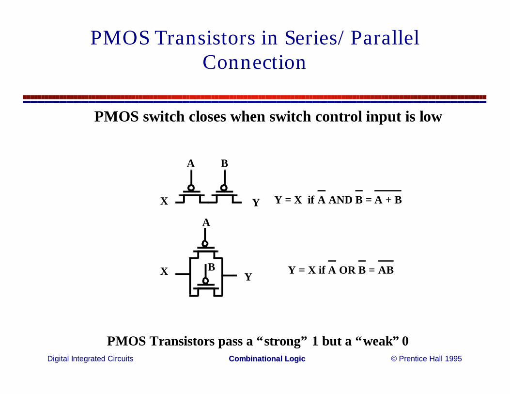
PMOS Transistors in Series/ParallelConnection
X Y
A B
Y = X if A AND B = A + B
X Y
A
B Y = X if A OR B = AB
PMOS Transistors pass a “strong” 1 but a “weak” 0
PMOS switch closes when switch control input is low
Digital Integrated Circuits © Prentice Hall 1995Combinational Combinational LogicLogic
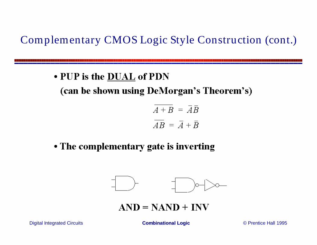
Complementary CMOS Logic Style Construction (cont.)
Digital Integrated Circuits © Prentice Hall 1995Combinational Combinational LogicLogic
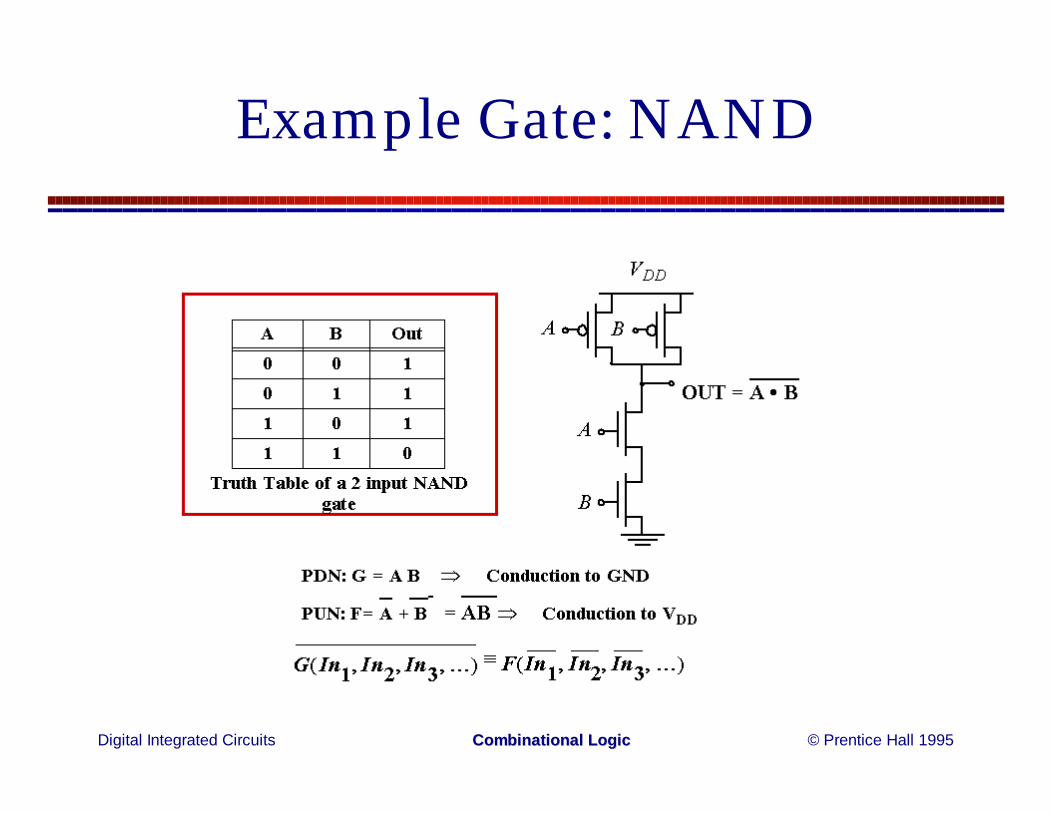
Example Gate: NAND
Digital Integrated Circuits © Prentice Hall 1995Combinational Combinational LogicLogic
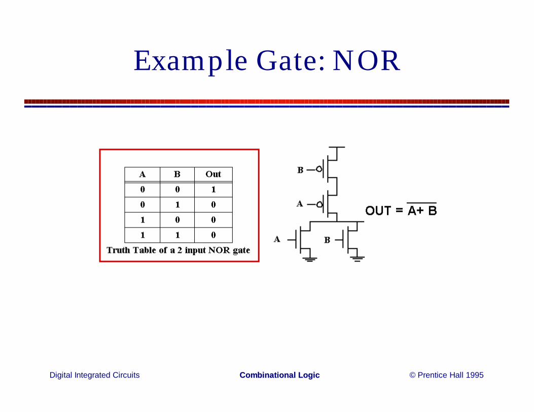
Example Gate: NOR
Digital Integrated Circuits © Prentice Hall 1995Combinational Combinational LogicLogic
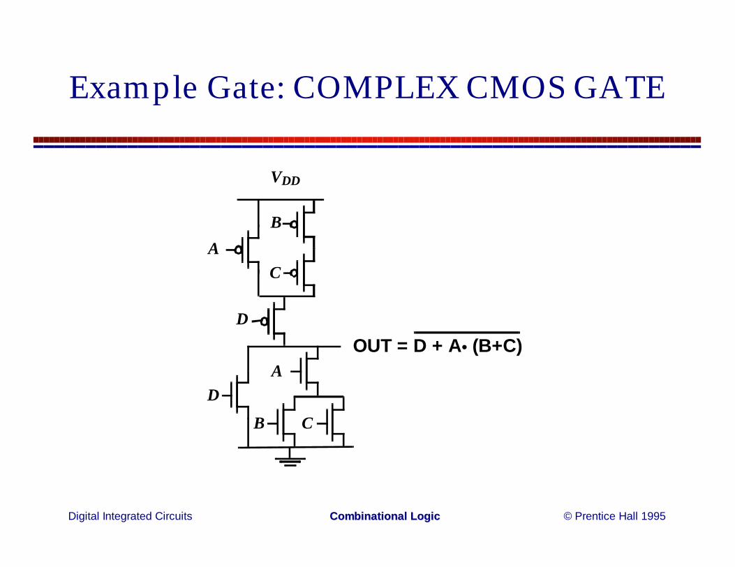
Example Gate: COMPLEX CMOS GATE
VDD
A
B
C
D
DA
B C
OUT = D + A• (B+C)
Digital Integrated Circuits © Prentice Hall 1995Combinational Combinational LogicLogic
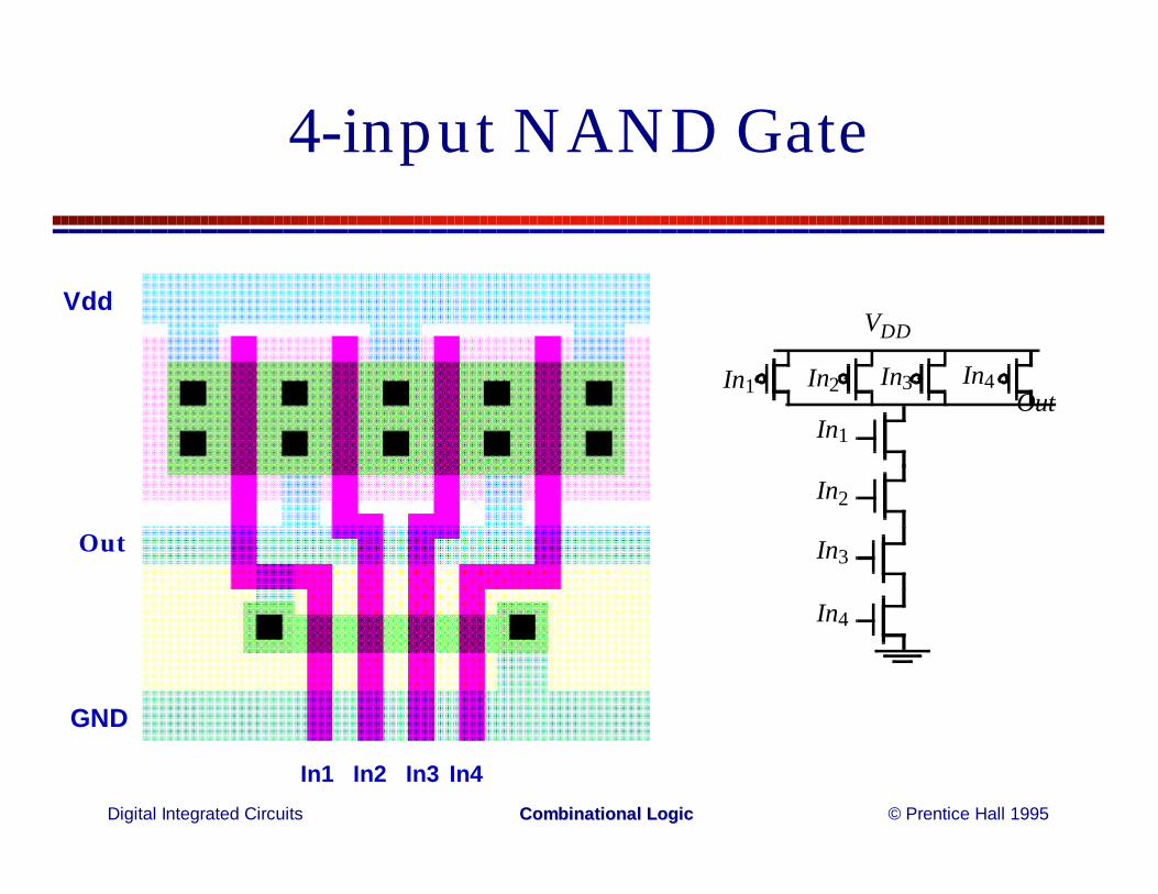
4-input NAND Gate
In3
In1
In2
In4
In1 In2 In3 In4
VDD
Out
In1 In2 In3 In4
Vdd
GND
Out
Digital Integrated Circuits © Prentice Hall 1995Combinational Combinational LogicLogic
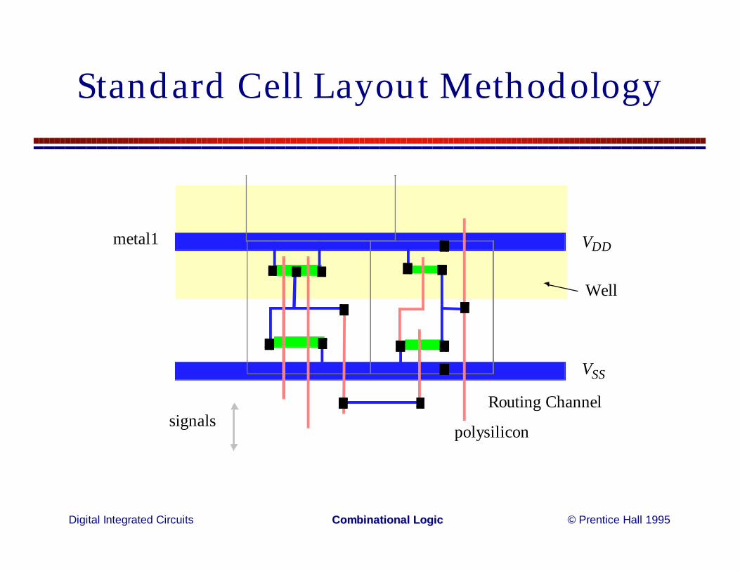
Standard Cell Layout Methodology
VDD
VSS
Well
signalsRouting Channel
metal1
polysilicon

Digital Integrated Circuits © Prentice Hall 1995Combinational Combinational LogicLogic
Two Versions of (a+b).c
a c b a b c
xx
GND
VDDVDD
GND
(a) Input order {a c b} (b) Input order {a b c}
Digital Integrated Circuits © Prentice Hall 1995Combinational Combinational LogicLogic
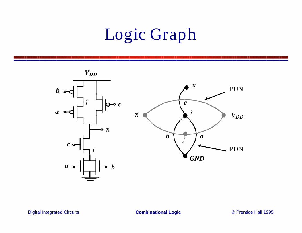
Logic Graph
VDD
c
a
x
b
ca
b
GND
x
VDDx
c
b a
i
j
i
jPDN
PUN
Digital Integrated Circuits © Prentice Hall 1995Combinational Combinational LogicLogic
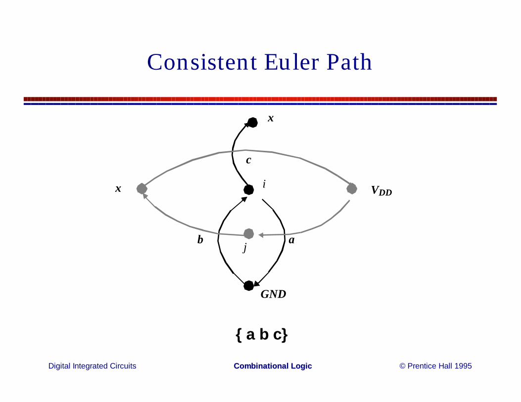
Consistent Euler Path
GND
x
VDDx
c
b a
i
j
{ a b c}
Digital Integrated Circuits © Prentice Hall 1995Combinational Combinational LogicLogic
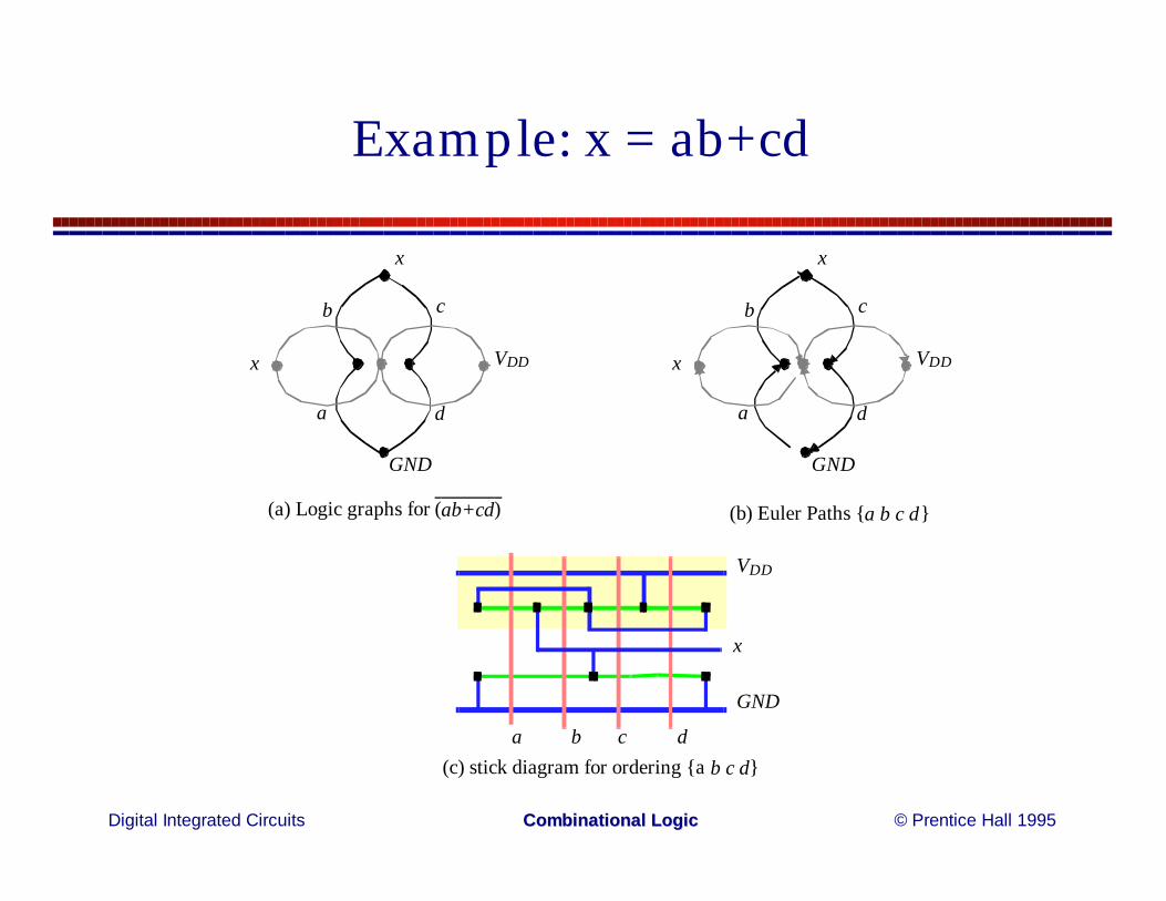
Example: x = ab+cd
GND
x
a
b c
d
VDDx
GND
x
a
b c
d
VDDx
(a) Logic graphs for (ab+cd) (b) Euler Paths {a b c d}
a c d
x
VDD
GND
(c) stick diagram for ordering {a b c d}b
Digital Integrated Circuits © Prentice Hall 1995Combinational Combinational LogicLogic
Properties of Complementary CMOS Gates
High noise margins: VOH and VOL are at VDD and GND, respectively.
No static power consumption:There never exists a direct path between VDD and VSS (GND) in steady-state mode.
Comparable rise and fall times:(under the appropriate scaling conditions)
Digital Integrated Circuits © Prentice Hall 1995Combinational Combinational LogicLogic
Properties of Complementary CMOSGates
High noise margins: VOH and VOL are at VDD and GND, respectively.
No static power consumption:There never exists a direct path between VDD and VSS (GND) in steady-state mode.
Comparable rise and fall times:(under the appropriate scaling conditions)
Digital Integrated Circuits © Prentice Hall 1995Combinational Combinational LogicLogic
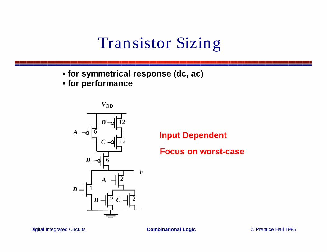
Transistor Sizing
VDD
AB
C
D
DA
B C
12
22
6
612
12
F
• for symmetrical response (dc, ac)• for performance
Focus on worst-case
Input Dependent
Digital Integrated Circuits © Prentice Hall 1995Combinational Combinational LogicLogic
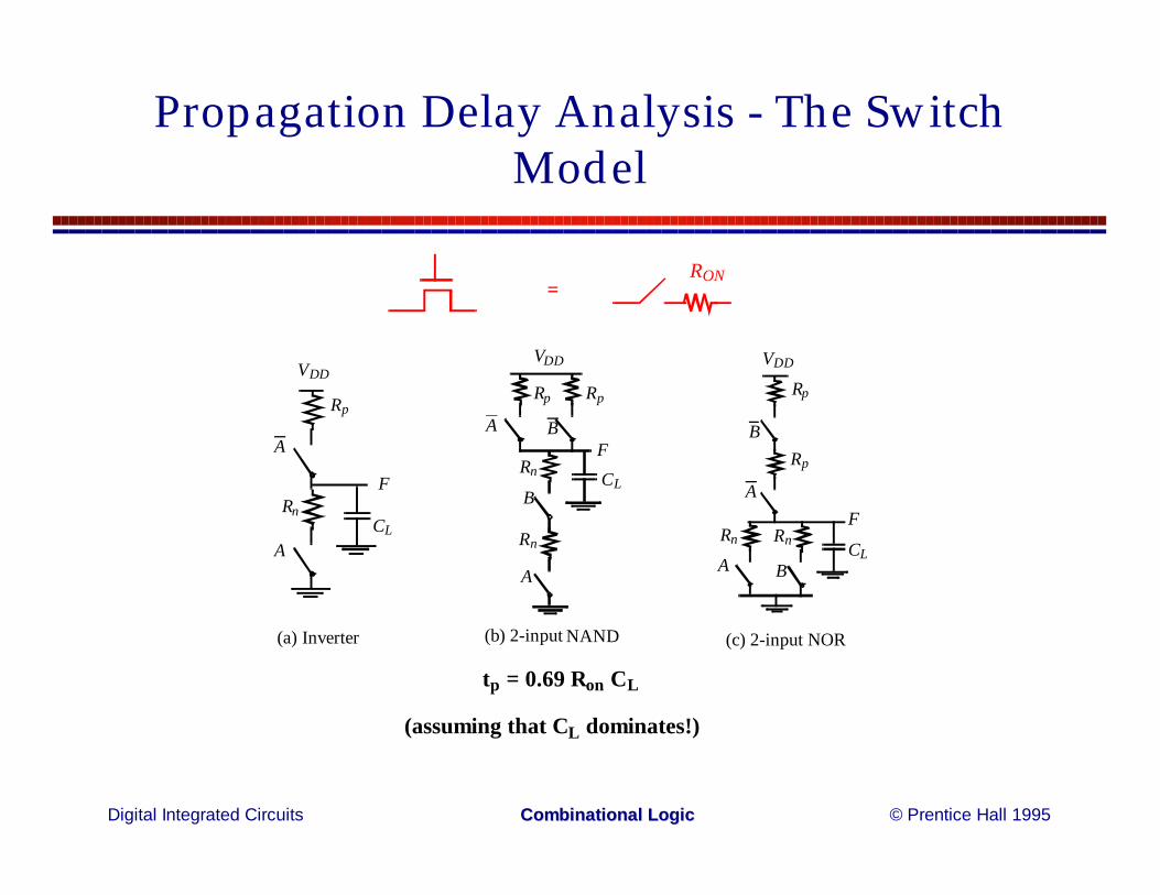
Propagation Delay Analysis - The SwitchModel
VDDVDDVDD
CL
F CL
CL
F
F
RpRp Rp Rp
Rp
Rn
Rn
Rn Rn Rn
AA
A
AA
A
B B
B
B
(a) Inverter (b) 2-input NAND (c) 2-input NOR
tp = 0.69 Ron CL
(assuming that CL dominates!)
= RON
Digital Integrated Circuits © Prentice Hall 1995Combinational Combinational LogicLogic
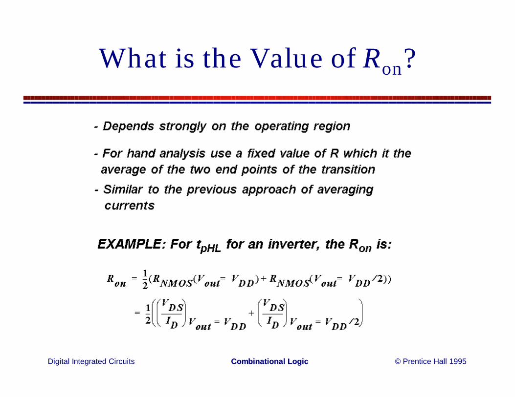
What is the Value of Ron?
Digital Integrated Circuits © Prentice Hall 1995Combinational Combinational LogicLogic
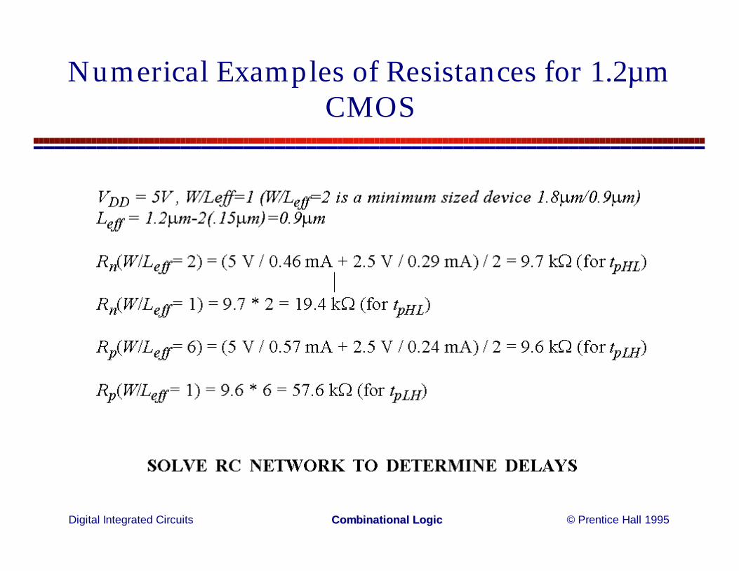
Numerical Examples of Resistances for 1.2µmCMOS
Digital Integrated Circuits © Prentice Hall 1995Combinational Combinational LogicLogic
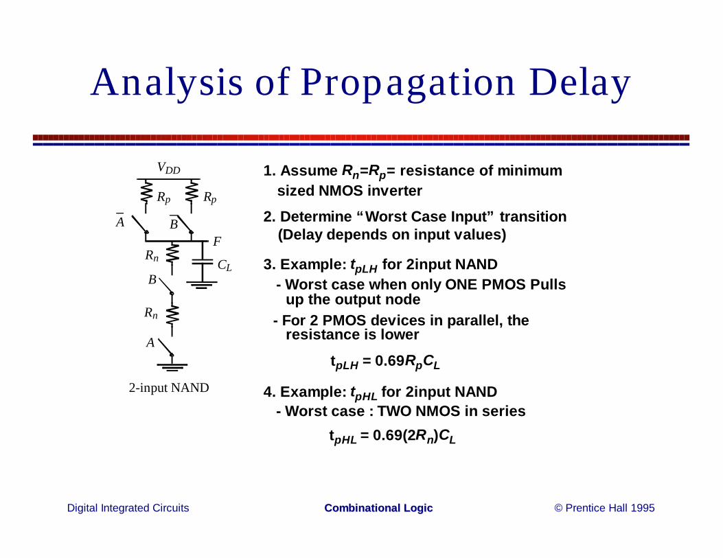
Analysis of Propagation Delay
VDD
CL
F
Rp Rp
Rn
Rn
A
A B
B
2-input NAND
1. Assume Rn=Rp= resistance of minimum sized NMOS inverter
2. Determine “Worst Case Input” transition(Delay depends on input values)
3. Example: tpLH for 2input NAND- Worst case when only ONE PMOS Pulls
up the output node- For 2 PMOS devices in parallel, the
resistance is lower
4. Example: tpHL for 2input NAND- Worst case : TWO NMOS in series
tpLH = 0.69RpCL
tpHL = 0.69(2Rn)CL
Digital Integrated Circuits © Prentice Hall 1995Combinational Combinational LogicLogic
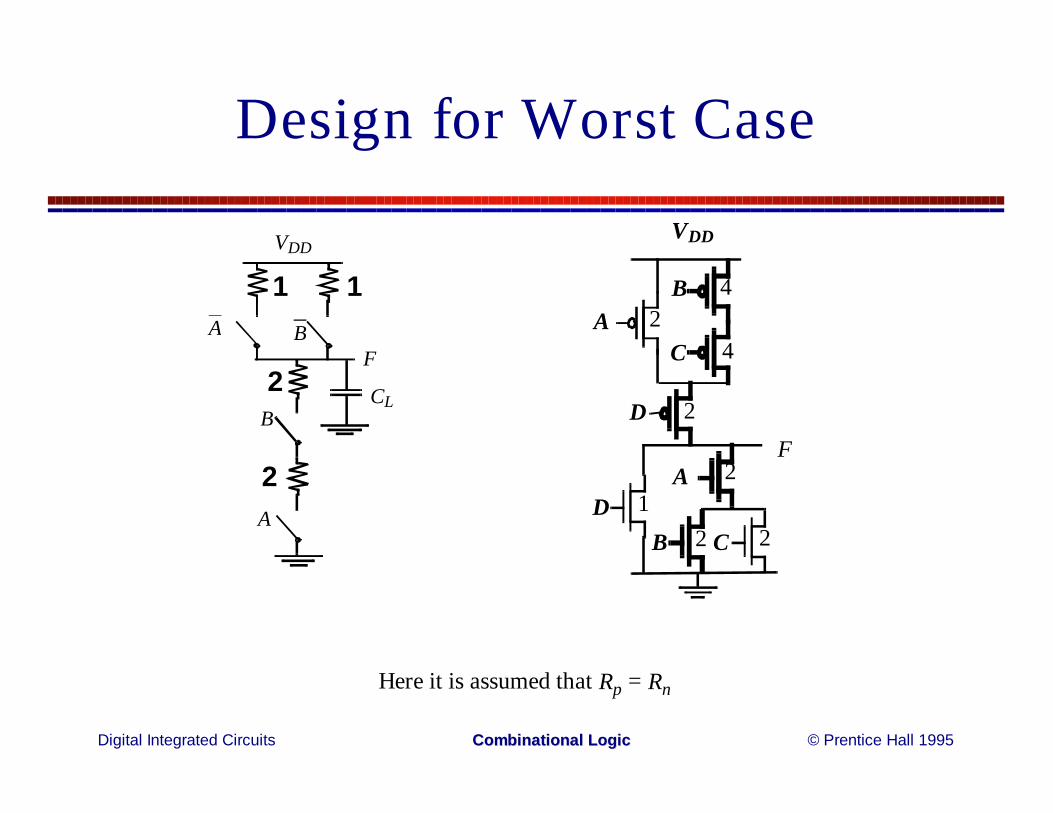
Design for Worst Case
VDD
CL
F
A
A B
B
2
2
1 1
VDD
AB
C
D
DA
B C
12
22
2
24
4
F
Here it is assumed that Rp = Rn
Digital Integrated Circuits © Prentice Hall 1995Combinational Combinational LogicLogic
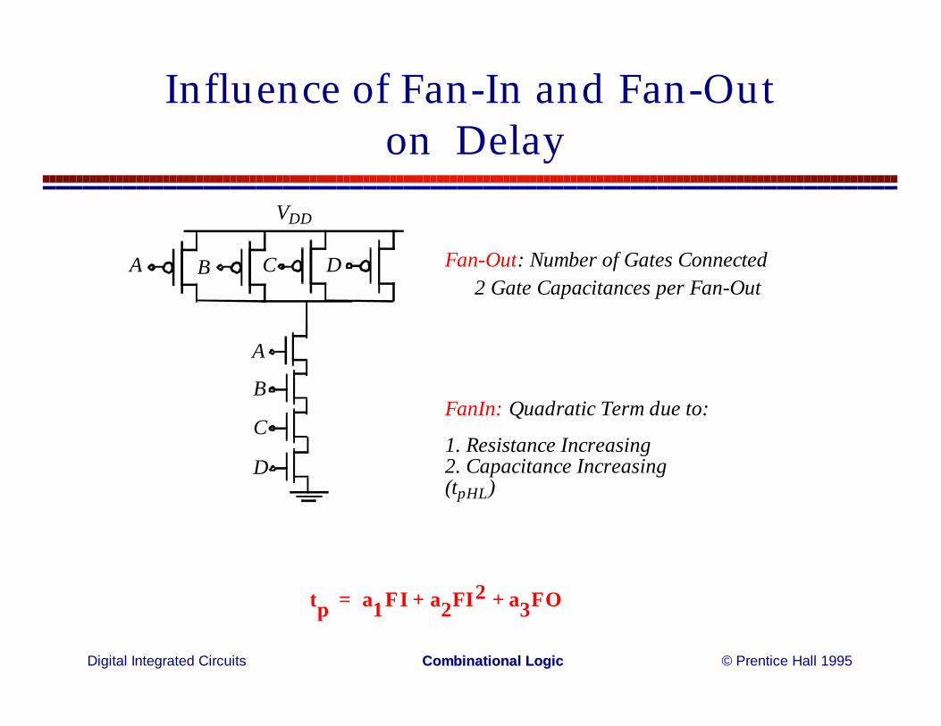
Influence of Fan-In and Fan-Out on Delay
VDD
A B
A
B
C
D
C D
tp a1FI a2FI2 a3FO+ +=
Fan-Out: Number of Gates Connected2 Gate Capacitances per Fan-Out
FanIn: Quadratic Term due to:
1. Resistance Increasing2. Capacitance Increasing(tpHL)
Digital Integrated Circuits © Prentice Hall 1995Combinational Combinational LogicLogic
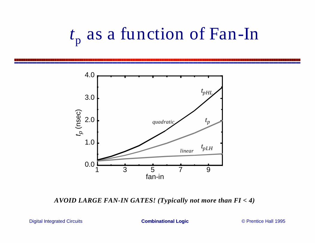
tp as a function of Fan-In
1 3 5 7 9fan-in
0.0
1.0
2.0
3.0
4.0t p
(nse
c)
tpHL
tp
tpLHlinear
quadratic
AVOID LARGE FAN-IN GATES! (Typically not more than FI < 4)

Digital Integrated Circuits © Prentice Hall 1995Combinational Combinational LogicLogic
Fast Complex Gate - DesignTechniques
• Transistor Sizing: As long as Fan-out Capacitance dominates
• Progressive Sizing:
CL
In1
InN
In3
In2
Out
C1
C2
C3
M1 > M2 > M3 > MN
M1
M2
M3
MN
Distributed RC-line
Can Reduce Delay with more than 30%!
Digital Integrated Circuits © Prentice Hall 1995Combinational Combinational LogicLogic
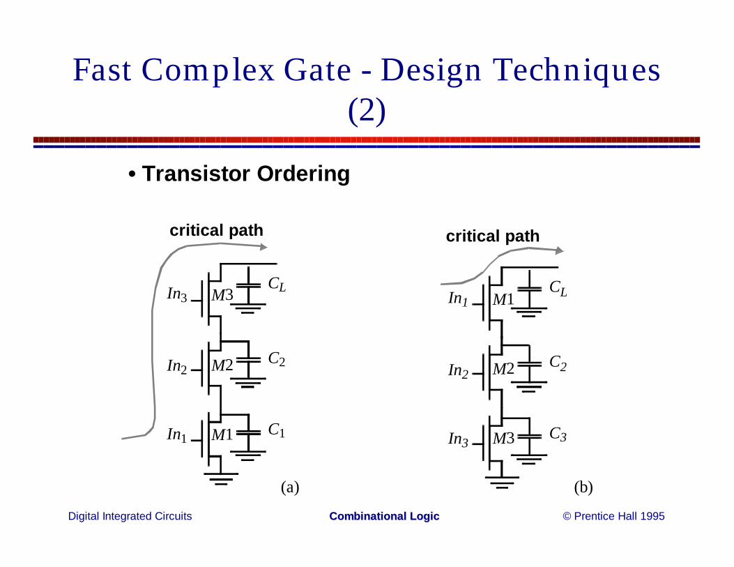
Fast Complex Gate - Design Techniques(2)
In1
In3
In2
C1
C2
CL
M1
M2
M3
In3
In1
In2
C3
C2
CL
M3
M2
M1
(a) (b)
• Transistor Ordering
critical pathcritical path

Digital Integrated Circuits © Prentice Hall 1995Combinational Combinational LogicLogic
Fast Complex Gate - Design Techniques(3)
• Improved Logic Design
Digital Integrated Circuits © Prentice Hall 1995Combinational Combinational LogicLogic
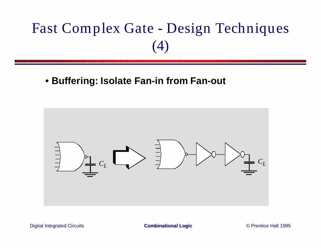
Fast Complex Gate - Design Techniques(4)
• Buffering: Isolate Fan-in from Fan-out
CLCL

Digital Integrated Circuits © Prentice Hall 1995Combinational Combinational LogicLogic
Example: Full Adder
VDD
VDD
VDD
VDD
A B
Ci
S
Co
X
B
A
Ci A
BBA
Ci
A B Ci
Ci
B
A
Ci
A
B
BA
Co = AB + Ci(A+B)
28 transistors
Digital Integrated Circuits © Prentice Hall 1995Combinational Combinational LogicLogic
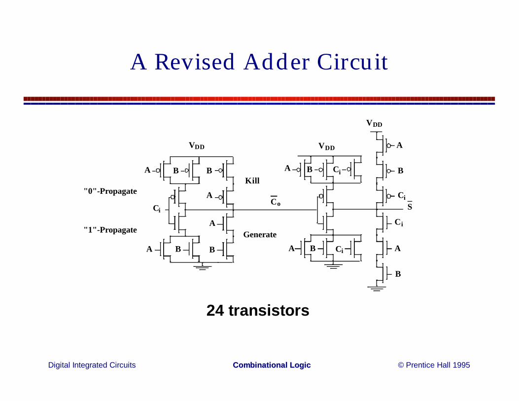
A Revised Adder Circuit
VDD
Ci
A
BBA
B
A
A BKill
Generate"1"-Propagate
"0"-Propagate
VDD
Ci
A B Ci
Ci
B
A
Ci
A
BBA
VDD
SCo
24 transistors
Digital Integrated Circuits © Prentice Hall 1995Combinational Combinational LogicLogic
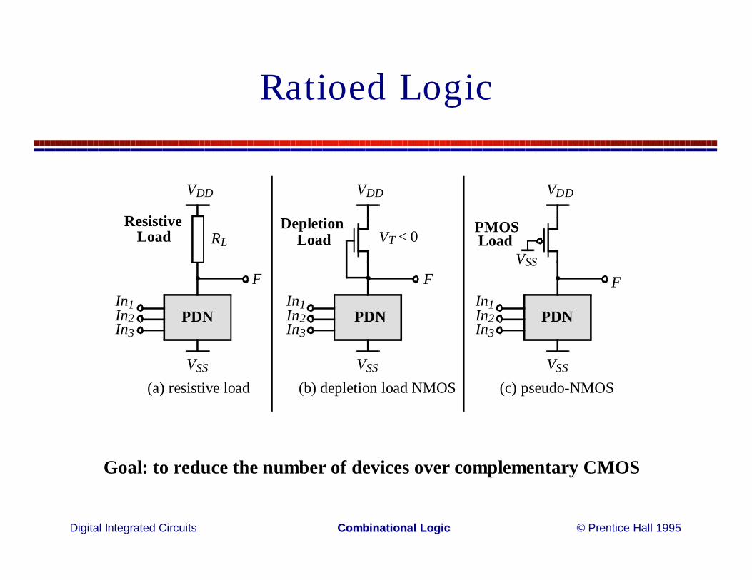
Ratioed Logic
VDD
VSS
PDNIn1In2In3
F
RLLoad
VDD
VSS
In1In2In3
F
VDD
VSS
PDNIn1In2In3
FVSS
PDN
Resistive DepletionLoad
PMOSLoad
(a) resistive load (b) depletion load NMOS (c) pseudo-NMOS
VT < 0
Goal: to reduce the number of devices over complementary CMOS
Digital Integrated Circuits © Prentice Hall 1995Combinational Combinational LogicLogic
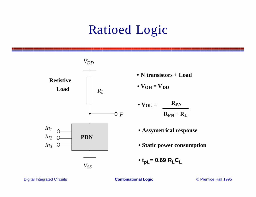
Ratioed Logic
VDD
VSS
PDN
In1
In2
In3
F
RLLoadResistive
N transistors + Load
• VOH = VDD
• VOL = RPN
RPN + RL
• Assymetrical response
• Static power consumption
•
• tpL= 0.69 RLCL

Digital Integrated Circuits © Prentice Hall 1995Combinational Combinational LogicLogic
Active Loads
VDD
VSS
In1In2In3
F
VDD
VSS
PDNIn1In2In3
F
VSS
PDN
DepletionLoad
PMOSLoad
depletion load NMOS pseudo-NMOS
VT < 0
Digital Integrated Circuits © Prentice Hall 1995Combinational Combinational LogicLogic
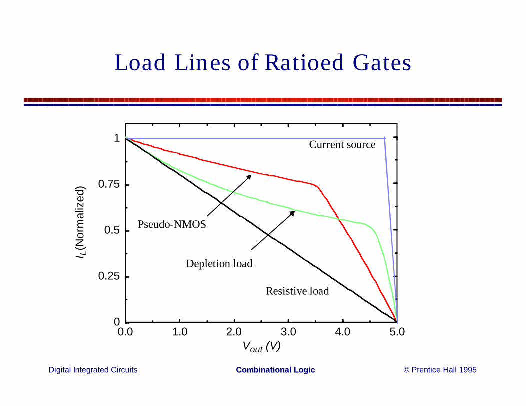
Load Lines of Ratioed Gates
0.0 1.0 2.0 3.0 4.0 5.0Vout (V)
0
0.25
0.5
0.75
1
I L(N
orm
aliz
ed)
Resistive load
Pseudo-NMOS
Depletion load
Current source
Digital Integrated Circuits © Prentice Hall 1995Combinational Combinational LogicLogic
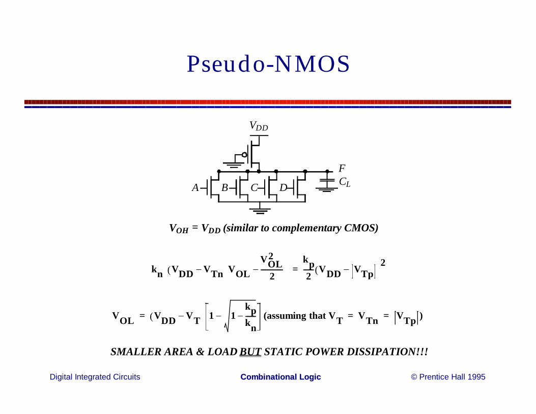
Pseudo-NMOS
VDD
A B C D
FCL
VOH = VDD (similar to complementary CMOS)
kn VDD VTn–( )VOLVOL
2
2-------------–
kp
2------ VDD VTp–( )
2=
VOL VDD VT–( ) 1 1kpkn------–– (assuming that VT VTn VTp )= = =
SMALLER AREA & LOAD BUT STATIC POWER DISSIPATION!!!
Digital Integrated Circuits © Prentice Hall 1995Combinational Combinational LogicLogic
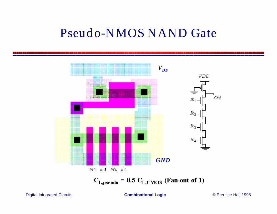
Pseudo-NMOS NAND Gate
VDD
GND
Digital Integrated Circuits © Prentice Hall 1995Combinational Combinational LogicLogic
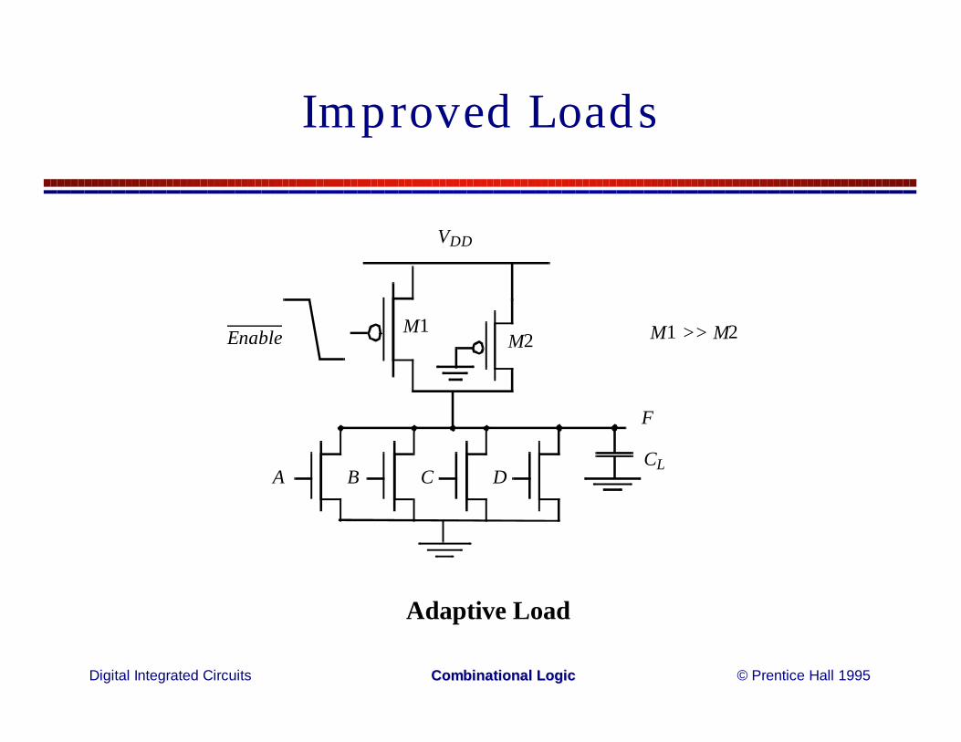
Improved Loads
A B C D
F
CL
M1M2 M1 >> M2Enable
VDD
Adaptive Load
Digital Integrated Circuits © Prentice Hall 1995Combinational Combinational LogicLogic
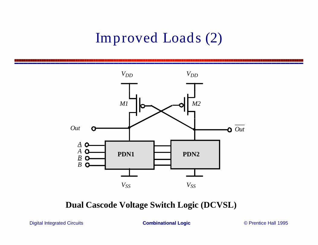
Improved Loads (2)
VDD
VSS
PDN1
Out
VDD
VSS
PDN2
Out
AABB
M1 M2
Dual Cascode Voltage Switch Logic (DCVSL)
Digital Integrated Circuits © Prentice Hall 1995Combinational Combinational LogicLogic
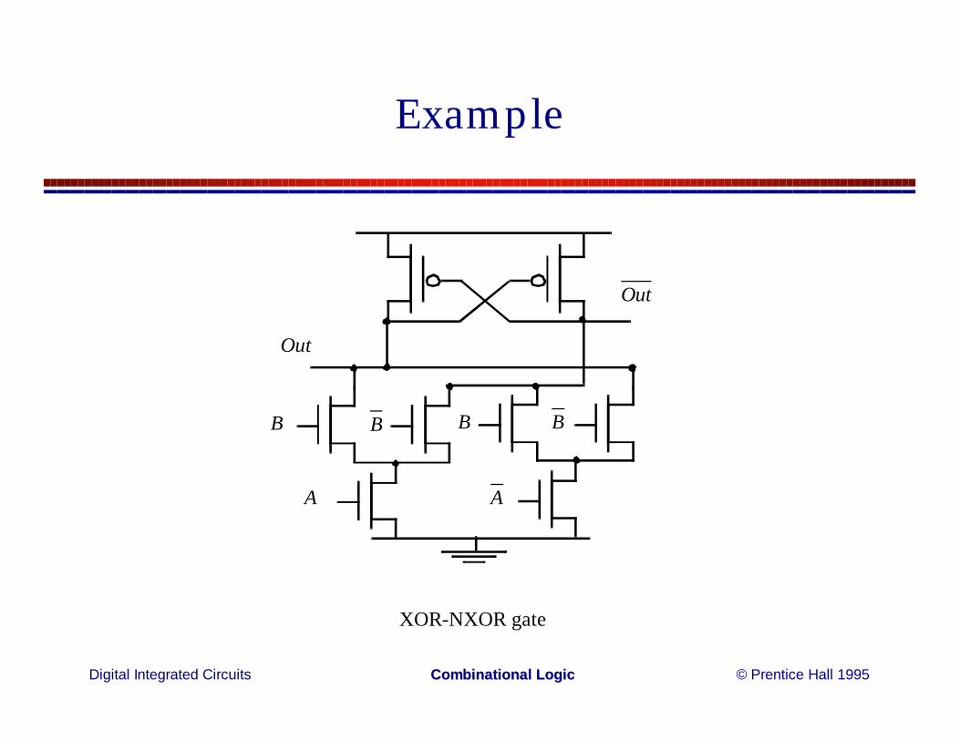
Example
B
A A
B B B
Out
Out
XOR-NXOR gate
Digital Integrated Circuits © Prentice Hall 1995Combinational Combinational LogicLogic
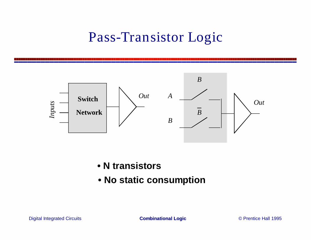
Pass-Transistor LogicIn
puts Switch
Network
OutOut
A
B
B
B
• N transistors• No static consumption
Digital Integrated Circuits © Prentice Hall 1995Combinational Combinational LogicLogic
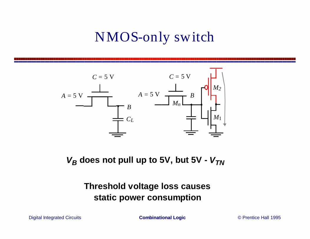
NMOS-only switch
A = 5 V
B
C = 5 V
CL
A = 5 V
C = 5 V
BM2
M1
Mn
Threshold voltage loss causesstatic power consumption
VB does not pull up to 5V, but 5V - VTN
Digital Integrated Circuits © Prentice Hall 1995Combinational Combinational LogicLogic
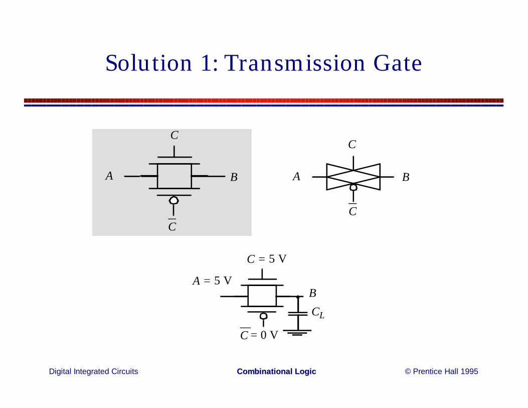
Solution 1: Transmission Gate
A B
C
C
A B
C
C
BCL
C = 0 V
A = 5 V
C = 5 V
Digital Integrated Circuits © Prentice Hall 1995Combinational Combinational LogicLogic
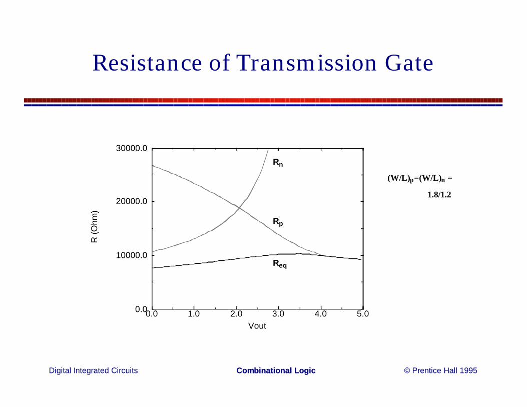
Resistance of Transmission Gate
(W/L)p=(W/L)n =
1.8/1.2
0.0 1.0 2.0 3.0 4.0 5.0Vout
0.0
10000.0
20000.0
30000.0
R (O
hm)
Rn
Req
Rp
Digital Integrated Circuits © Prentice Hall 1995Combinational Combinational LogicLogic
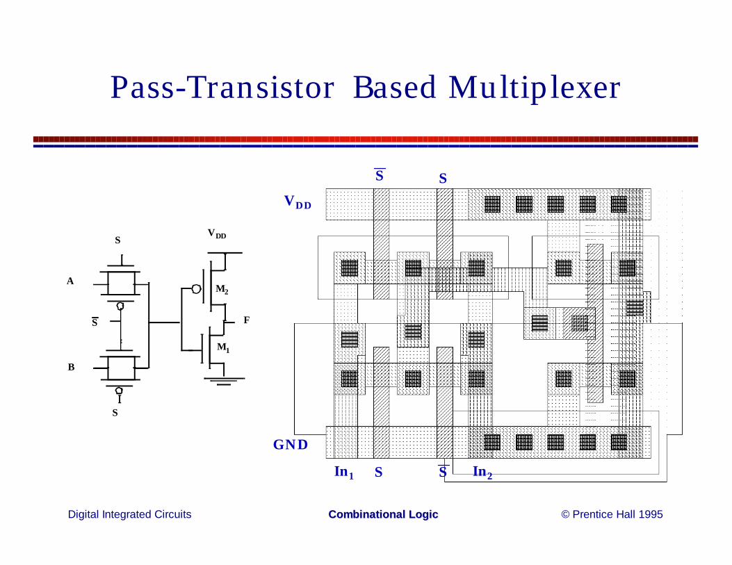
Pass-Transistor Based Multiplexer
AM2
M1
B
S
S
S F
VDD
GND
VDD
In1 In2S S
S S

Digital Integrated Circuits © Prentice Hall 1995Combinational Combinational LogicLogic
Transmission Gate XOR
A
B
F
B
A
B
BM1
M2
M3/M4

Digital Integrated Circuits © Prentice Hall 1995Combinational Combinational LogicLogic
Delay in Transmission Gate Networks
V1 Vi-1
C
5 5
0 0
Vi Vi+1
CC
5
0
Vn-1 Vn
CC
5
0
In
V1 Vi Vi+1
C
Vn-1 Vn
CC
InReqReq Req Req
CC
(a)
(b)
C
Req Req
C C
Req
C C
Req Req
C C
Req
CIn
m
(c)
Digital Integrated Circuits © Prentice Hall 1995Combinational Combinational LogicLogic
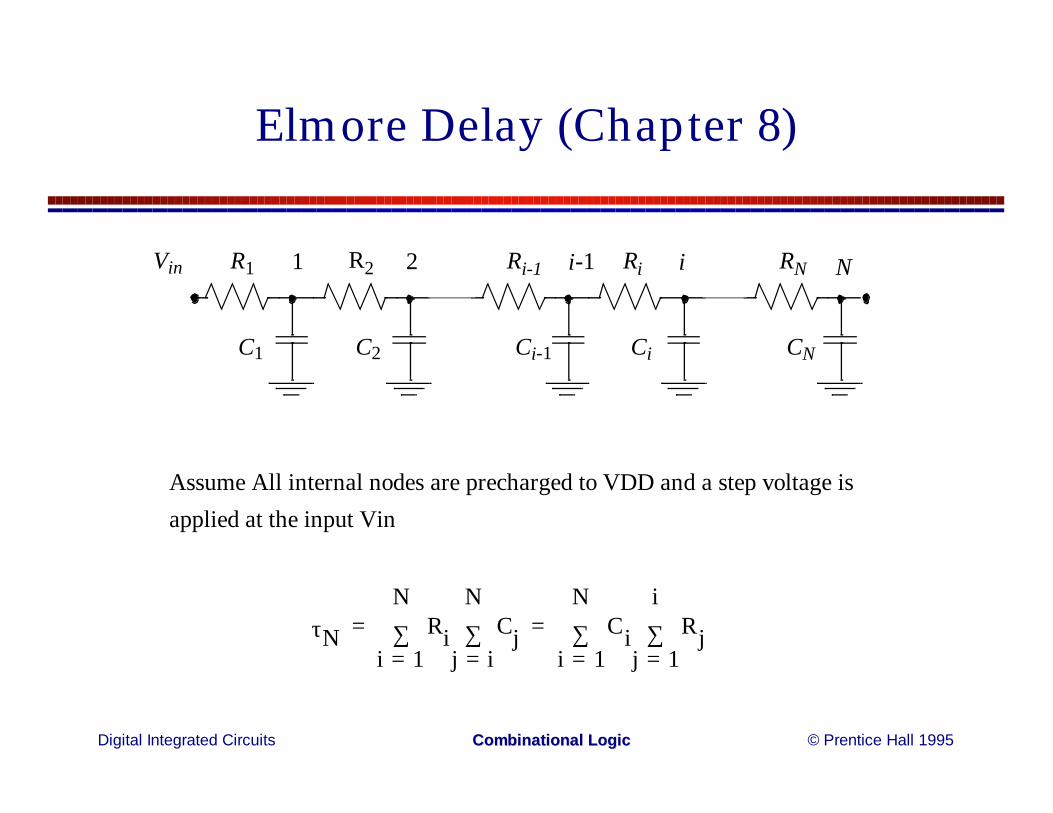
Elmore Delay (Chapter 8)
R1
C1
R2
C2
Ri-1
Ci-1
Ri
Ci
RN
CN
Vin N1 2 i-1 i
Assume All internal nodes are precharged to VDD and a step voltage isapplied at the input Vin
τN Ri Cjj i=
N
∑i 1=
N
∑ Ci Rjj 1=
i
∑i 1=
N
∑= =
Digital Integrated Circuits © Prentice Hall 1995Combinational Combinational LogicLogic
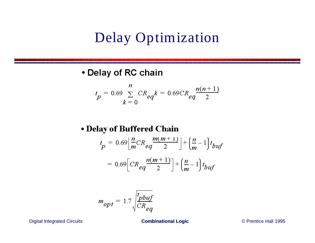
Delay Optimization
Digital Integrated Circuits © Prentice Hall 1995Combinational Combinational LogicLogic
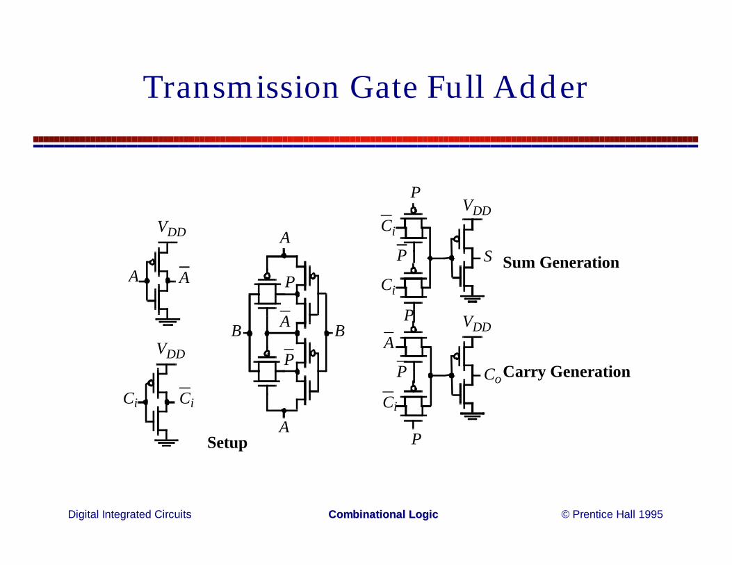
Transmission Gate Full Adder
A
B
P
Ci
VDDA
A A
VDD
Ci
A
P
AB
VDD
VDD
Ci
Ci
Co
S
Ci
P
P
P
P
P
Sum Generation
Carry Generation
Setup
Digital Integrated Circuits © Prentice Hall 1995Combinational Combinational LogicLogic
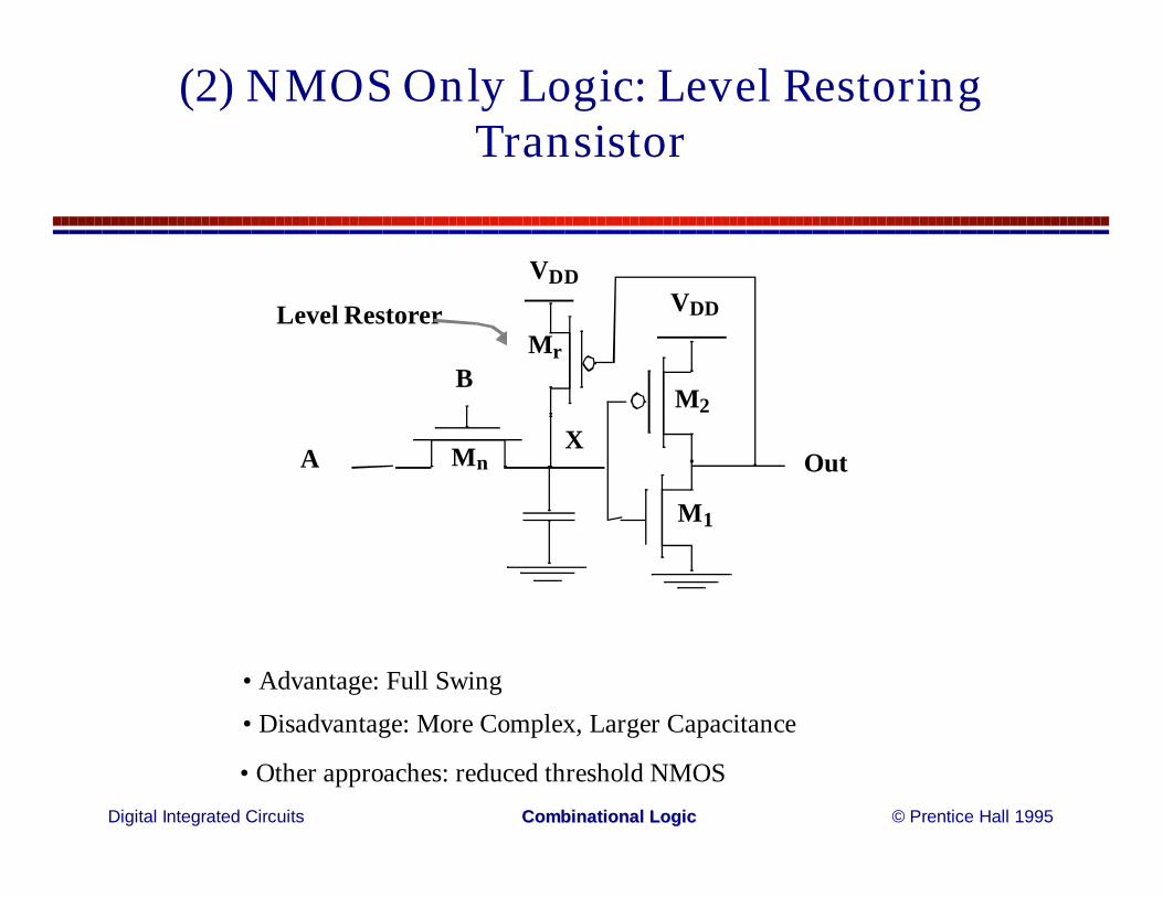
(2) NMOS Only Logic: Level RestoringTransistor
M2
M1
Mn
Mr
OutA
B
VDDVDDLevel Restorer
X
• Advantage: Full Swing
• Disadvantage: More Complex, Larger Capacitance
• Other approaches: reduced threshold NMOS
Digital Integrated Circuits © Prentice Hall 1995Combinational Combinational LogicLogic
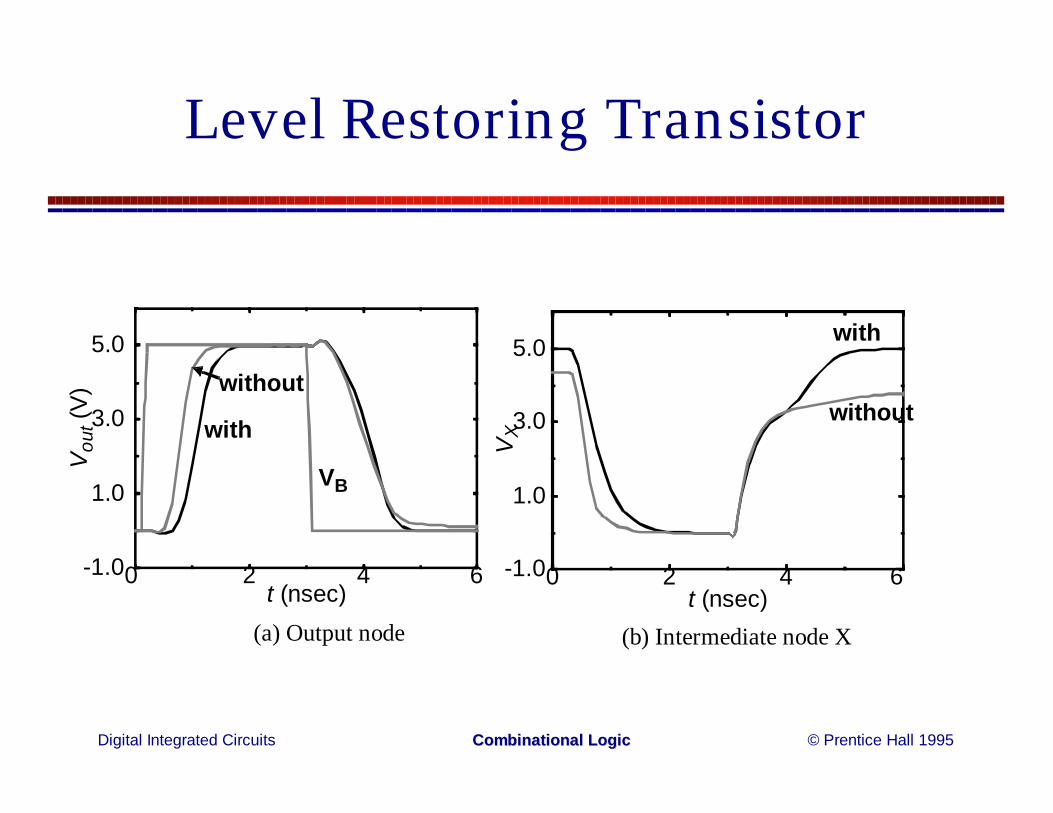
Level Restoring Transistor
(a) Output node (b) Intermediate node X
0 2 4 6t (nsec)
-1.0
1.0
3.0
5.0
Vou
t (V
)
0 2 4t (nsec)
-1.0
1.0
3.0
5.0
VX
with
without
VB
with
without
6
Digital Integrated Circuits © Prentice Hall 1995Combinational Combinational LogicLogic
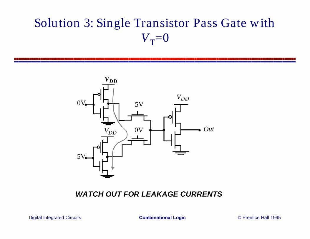
Solution 3: Single Transistor Pass Gate withVT=0
Out
VDD
VDD
5V
VDD
0V 5V
0V
WATCH OUT FOR LEAKAGE CURRENTS
Digital Integrated Circuits © Prentice Hall 1995Combinational Combinational LogicLogic
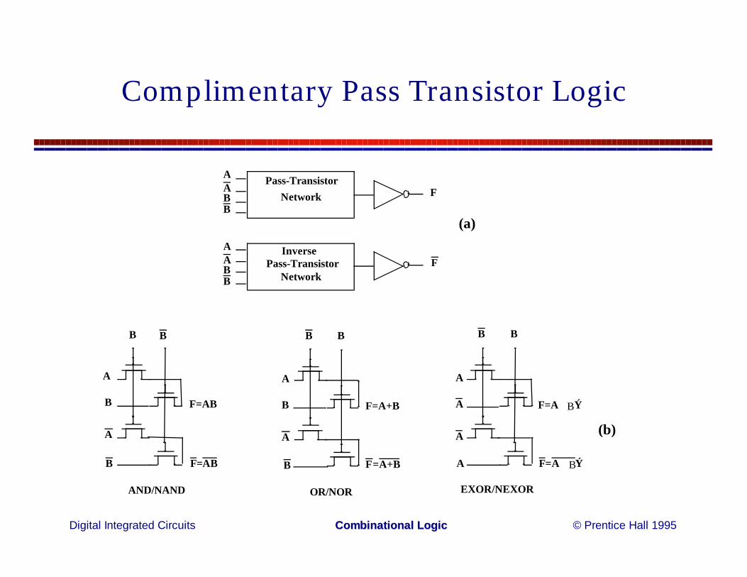
Complimentary Pass Transistor Logic
A
B
A
B
B B B B
A
B
A
B
F=AB
F=AB
F=A+B
F=A+B
B B
A
A
A
A
F=A⊕ ΒÝ
F=A⊕ ΒÝ
OR/NOR EXOR/NEXORAND/NAND
F
F
Pass-TransistorNetwork
Pass-TransistorNetwork
AABB
AABB
Inverse
(a)
(b)
Digital Integrated Circuits © Prentice Hall 1995Combinational Combinational LogicLogic
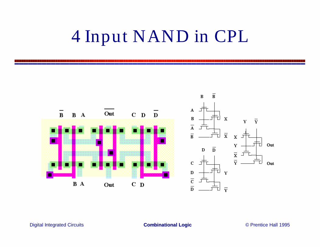
4 Input NAND in CPL
Digital Integrated Circuits © Prentice Hall 1995Combinational Combinational LogicLogic
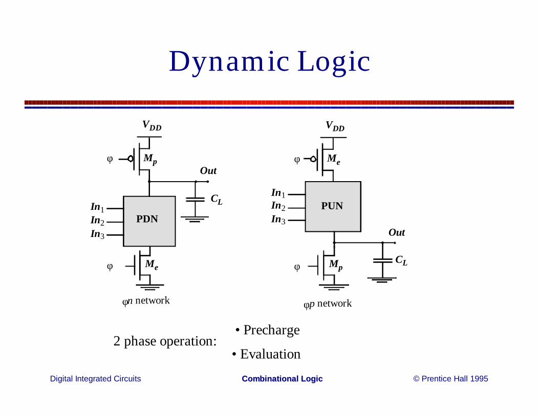
Dynamic Logic
Mp
Me
VDD
PDN
φ
In1In2In3
OutMe
Mp
VDD
PUN
φ
In1In2In3
φ
φ
Out
CL
CL
φp networkφn network
2 phase operation:• Evaluation
• Precharge
Digital Integrated Circuits © Prentice Hall 1995Combinational Combinational LogicLogic
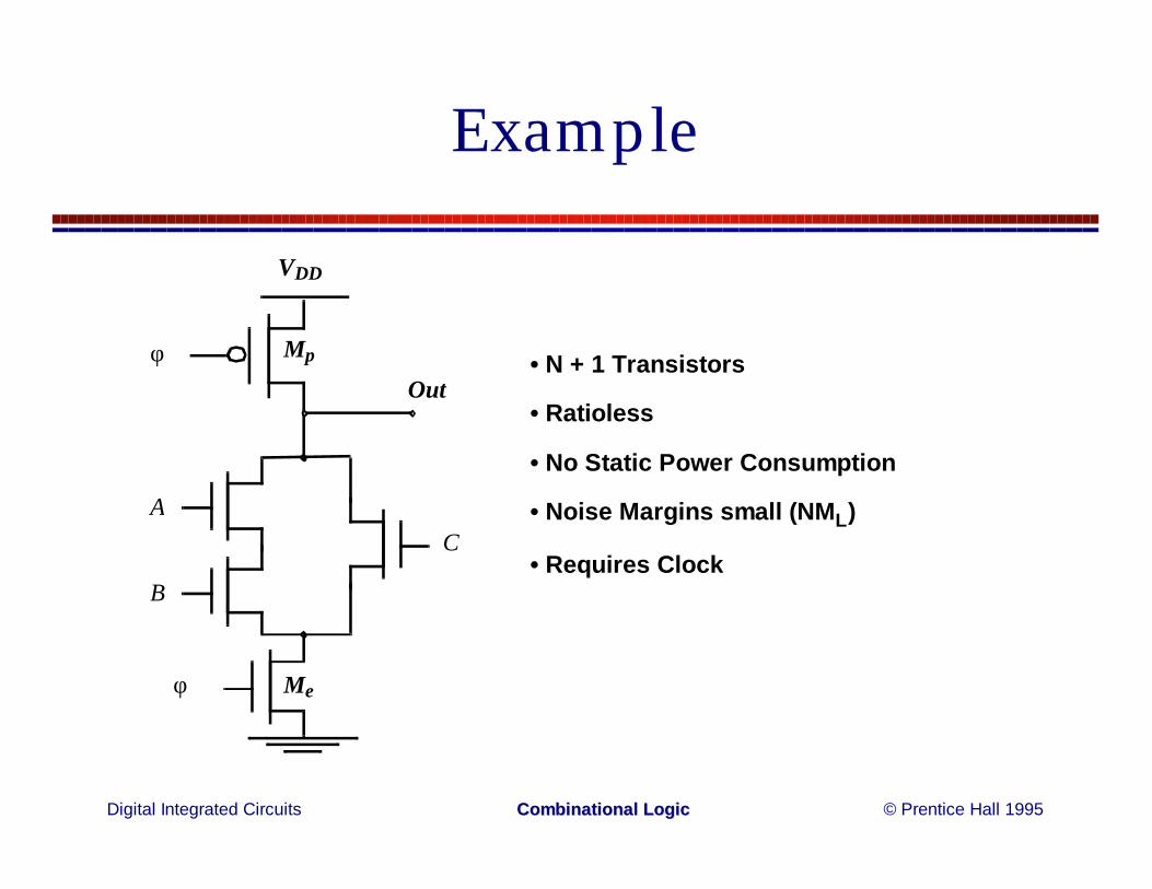
Example
Mp
Me
VDD
φOut
φ
A
B
C
• N + 1 Transistors
• Ratioless
• No Static Power Consumption
• Noise Margins small (NML)
• Requires Clock
Digital Integrated Circuits © Prentice Hall 1995Combinational Combinational LogicLogic
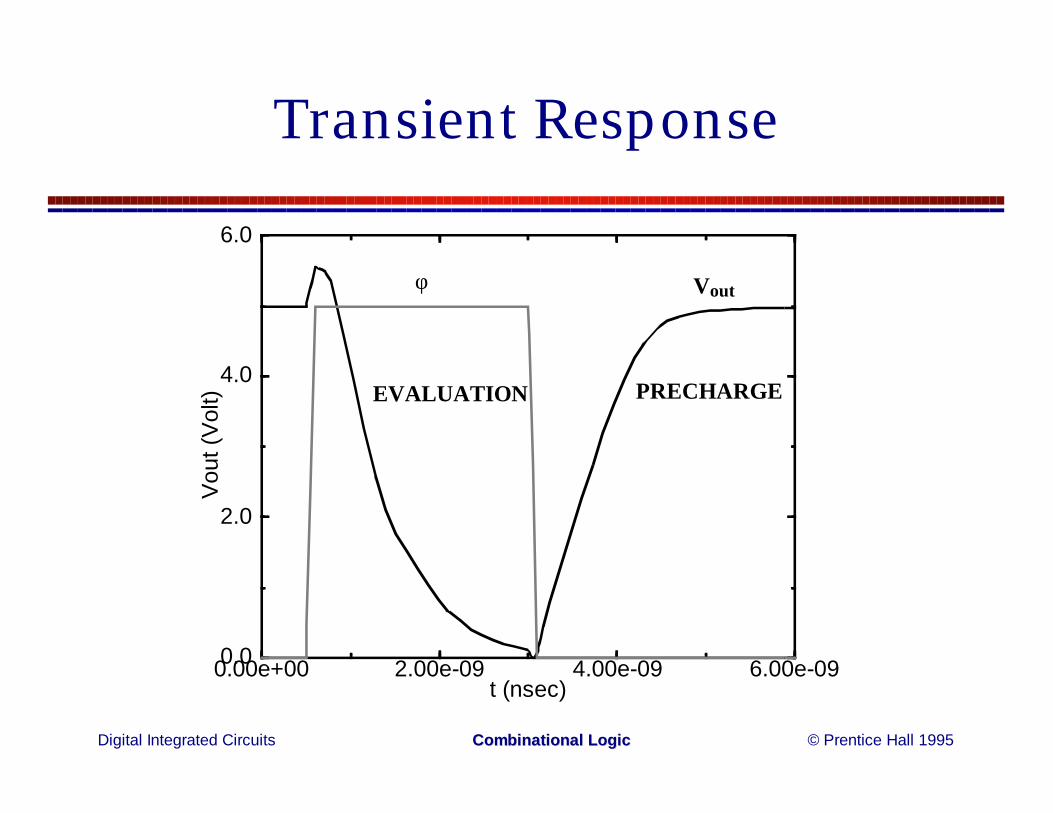
Transient Response
0.00e+00 2.00e-09 4.00e-09 6.00e-09t (nsec)
0.0
2.0
4.0
6.0V
out (
Vol
t)
φ Vout
PRECHARGEEVALUATION
Digital Integrated Circuits © Prentice Hall 1995Combinational Combinational LogicLogic
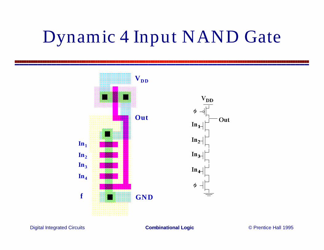
Dynamic 4 Input NAND Gate
In1
In2
In3
In4
Out
VDD
GNDφ
Digital Integrated Circuits © Prentice Hall 1995Combinational Combinational LogicLogic
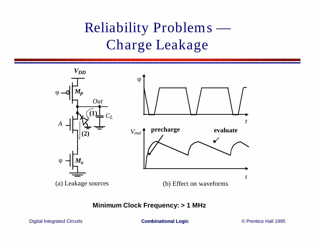
Reliability Problems —Charge Leakage
Mp
Me
VDD
φOut
φ
ACL
(1)
(2)
φ
t
t
Vout
(b) Effect on waveforms(a) Leakage sources
precharge evaluate
Minimum Clock Frequency: > 1 MHz
Digital Integrated Circuits © Prentice Hall 1995Combinational Combinational LogicLogic
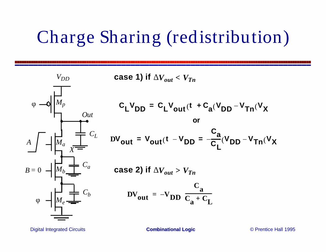
Charge Sharing (redistribution)
Mp
Me
VDD
φOut
φ
A
B = 0
CL
Ca
Cb
Ma
Mb
X
CLVDD CLVout t( ) Ca VDD VTn VX( )–( )+=
or
∆Vout Vout t( ) VDD–CaCL-------- VDD VTn VX( )–( )–= =
∆Vout VDD
CaCa CL+----------------------
–=
case 1) if ∆Vout < VTn
case 2) if ∆Vout > VTn
Digital Integrated Circuits © Prentice Hall 1995Combinational Combinational LogicLogic
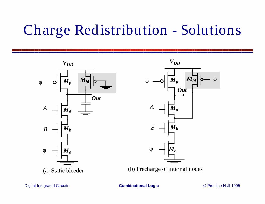
Charge Redistribution - Solutions
Mp
Me
VDD
φ
Out
φ
A
B
Ma
Mb
Mbl Mp
Me
VDD
φOut
φ
A
B
Ma
Mb
Mbl
(b) Precharge of internal nodes
φ
(a) Static bleeder
Digital Integrated Circuits © Prentice Hall 1995Combinational Combinational LogicLogic
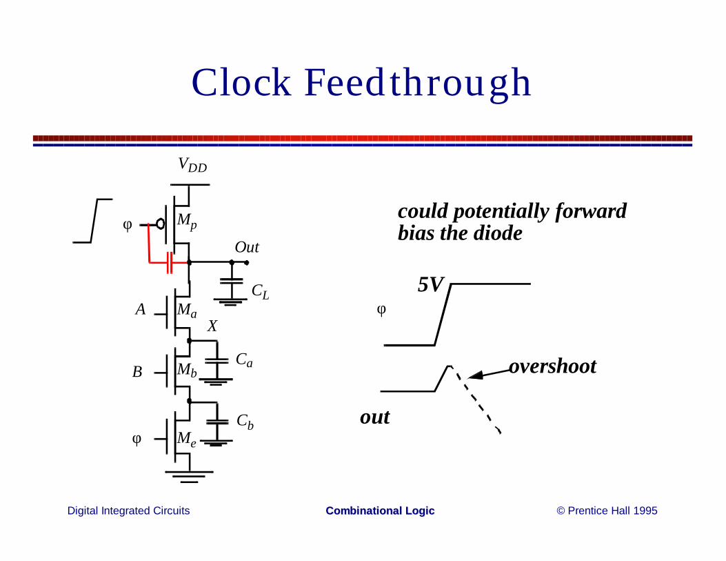
Clock Feedthrough
Mp
Me
VDD
φOut
φ
A
B
CL
Ca
Cb
Ma
Mb
Xφ
5V
overshoot
out
could potentially forwardbias the diode
Digital Integrated Circuits © Prentice Hall 1995Combinational Combinational LogicLogic
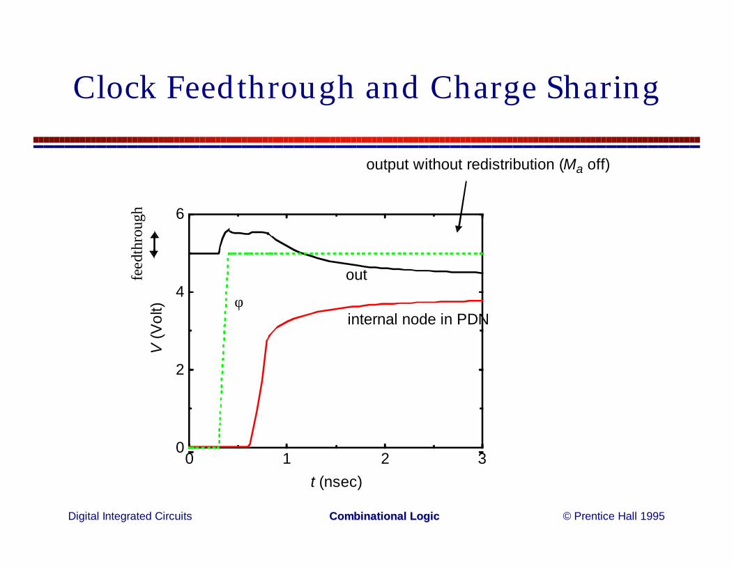
Clock Feedthrough and Charge Sharing
0 1 2 3t (nsec)
0
2
4
6
V (V
olt) φ
out
internal node in PDN
output without redistribution (Ma off)
feed
thro
ugh
Digital Integrated Circuits © Prentice Hall 1995Combinational Combinational LogicLogic
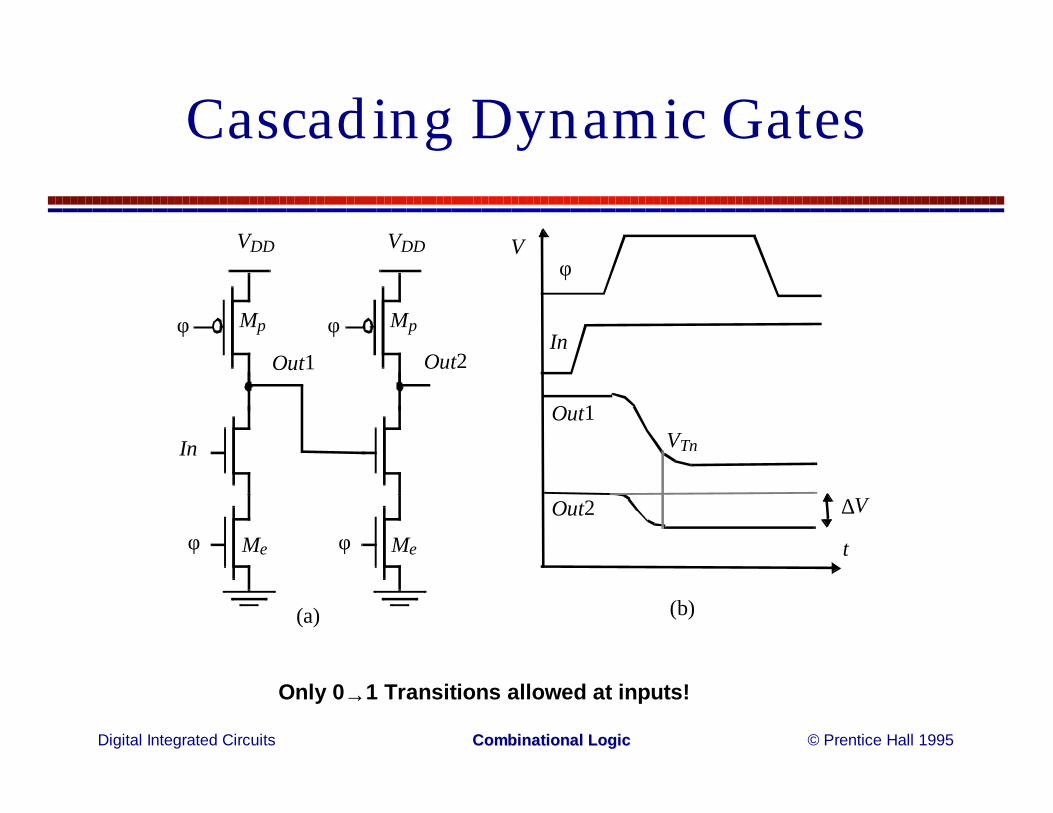
Cascading Dynamic Gates
Mp
Me
VDD
φ
φ
Mp
Me
VDD
φ
φ
In
Out1 Out2
φ
Out2
Out1
In
V
t
∆V
VTn
(a) (b)
Only 0→ 1 Transitions allowed at inputs!
Digital Integrated Circuits © Prentice Hall 1995Combinational Combinational LogicLogic
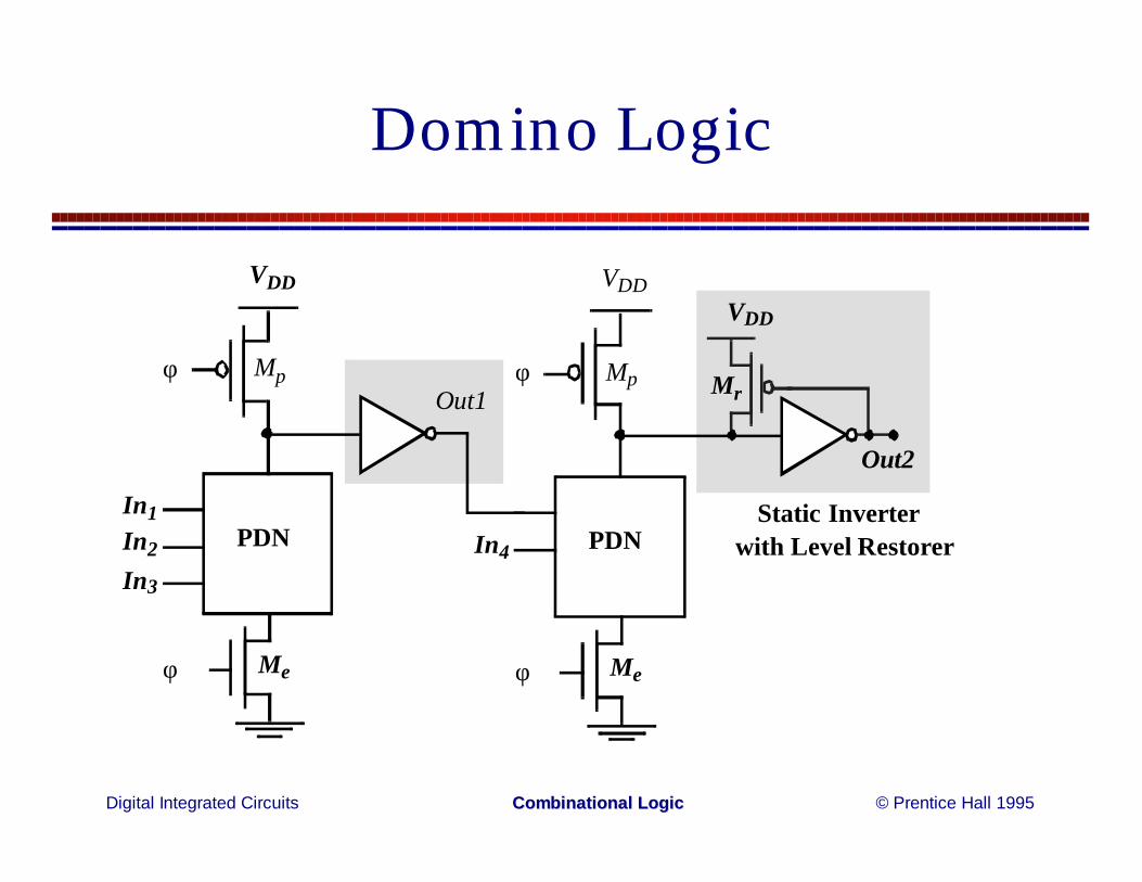
Domino Logic
Mp
Me
VDD
PDN
φ
In1In2
In3
Out1
φ
Mp
Me
VDD
PDN
φ
In4
φ
Out2
Mr
VDD
Static Inverterwith Level Restorer
Digital Integrated Circuits © Prentice Hall 1995Combinational Combinational LogicLogic
Domino Logic - Characteristics
• Only non-inverting logic
• Very fast - Only 1->0 transitions at input of inverter
move VM upwards by increasing PMOS
• Adding level restorer reduces leakage andcharge redistribution problems
• Optimize inverter for fan-out
Digital Integrated Circuits © Prentice Hall 1995Combinational Combinational LogicLogic
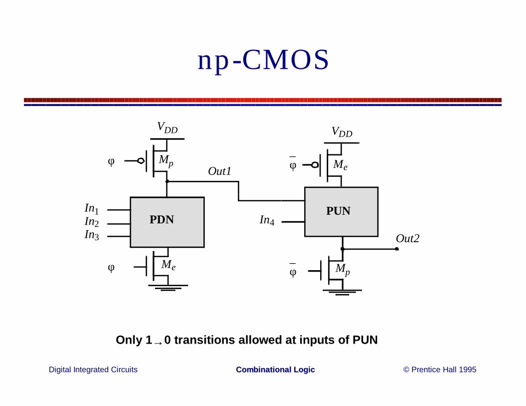
np-CMOS
Mp
Me
VDD
PDN
φ
In1In2In3
φ
Me
Mp
VDD
PUN
φ
In4
φOut1
Out2
Only 1→ 0 transitions allowed at inputs of PUN
Digital Integrated Circuits © Prentice Hall 1995Combinational Combinational LogicLogic
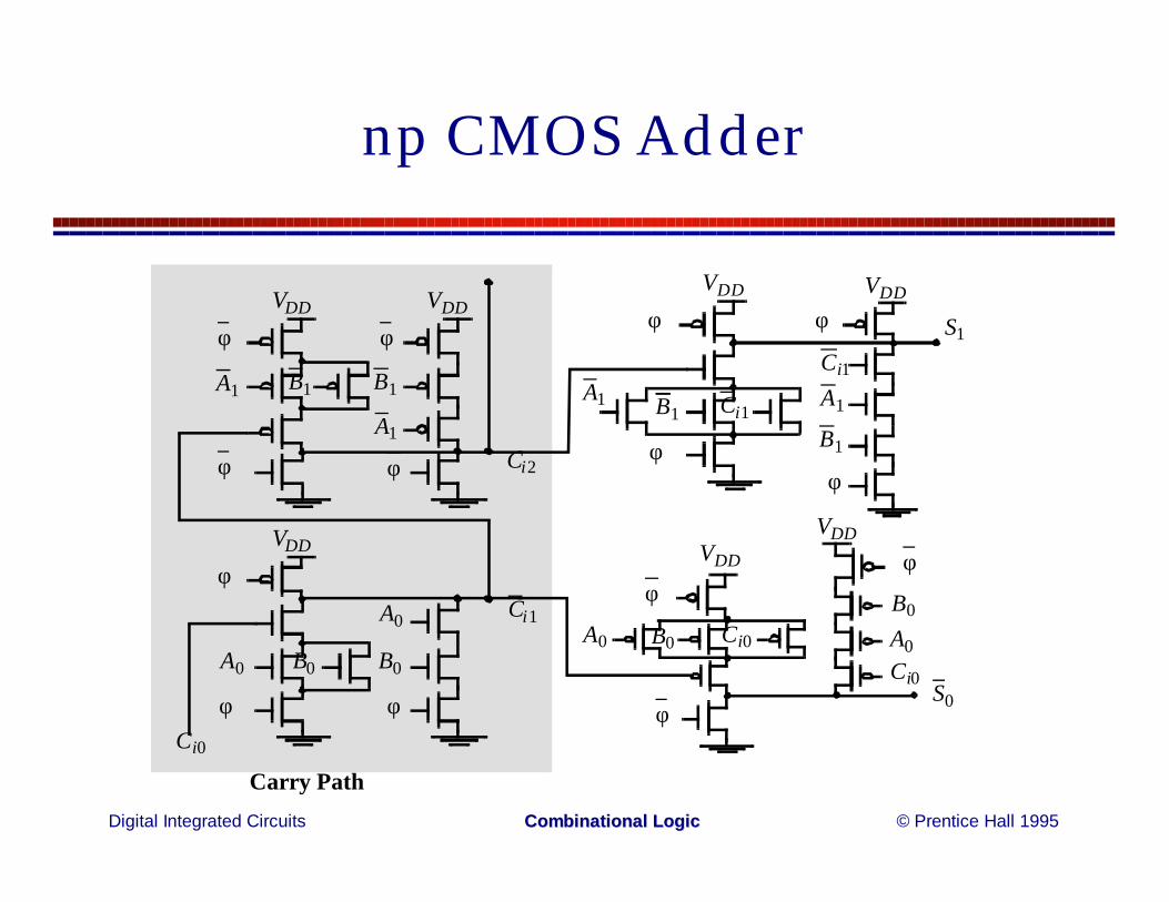
np CMOS Adder
VDD
φ
φCi0
A0 B0 B0
φ
A0
VDD
φ
B1
φA1
VDD
φ
φ
A1 B1
Ci1
Ci2
Ci0
Ci0
B0
A0B0
S0
A0
VDD
φ
φ
VDD
φ
VDD
φ
φ
B1 Ci1
B1
φ
A1A1
VDD
φ S1
Ci1
Carry Path
Digital Integrated Circuits © Prentice Hall 1995Combinational Combinational LogicLogic
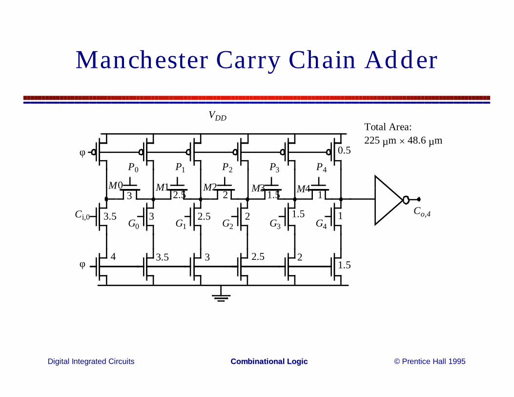
Manchester Carry Chain Adder
P0
Ci,0
P1
G0
P2
G1
P3
G2
P4
G3 G4
φ
φ
VDD
M0 M1 M2 M3 M4
Co,4
11.522.53
3.5 3 2.5 2 1.5 1
1.522.533.54
0.5
Total Area:225 µm × 48.6 µm
Digital Integrated Circuits © Prentice Hall 1995Combinational Combinational LogicLogic
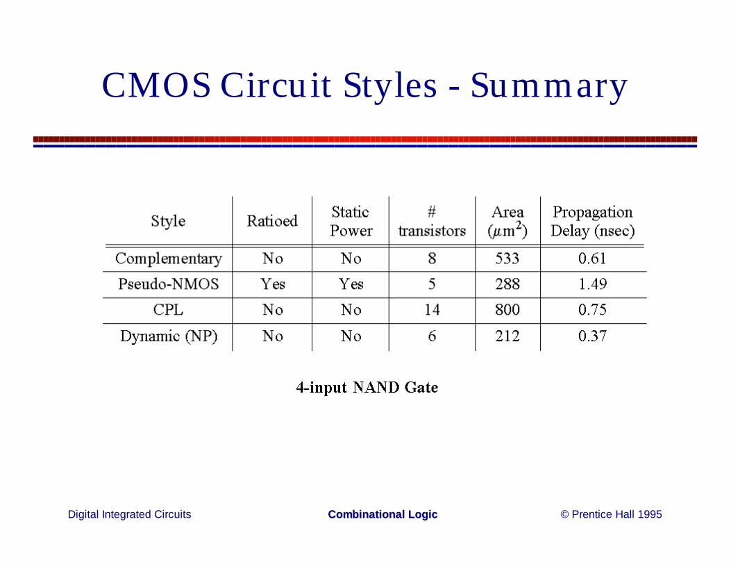
CMOS Circuit Styles - Summary