Combinational Logic Gates in CMOS - Purdue …vlsi/ECE559_Fall09/Notes/Logic...Combinational vs....
48
Combinational Logic Gates in CMOS References: Adapted from: Digital Integrated Circuits: A Design Perspective, J. Rabaey, Prentice Hall © UCB Principles of CMOS VLSI Design: A Systems Perspective, N. H. E. Weste, K. Eshraghian, Addison Wesley Adapted from: EE216A Lecture Notes by Prof. K. Bult © UCLA
Transcript of Combinational Logic Gates in CMOS - Purdue …vlsi/ECE559_Fall09/Notes/Logic...Combinational vs....
Combinational Logic Gates in CMOS
References:
Adapted from: Digital Integrated Circuits: A Design
Perspective, J. Rabaey, Prentice Hall © UCB
Principles of CMOS VLSI Design: A Systems Perspective,
N. H. E. Weste, K. Eshraghian, Addison Wesley
Adapted from: EE216A Lecture Notes by Prof. K. Bult ©
UCLA

Combinational vs. Sequential Logic
CombinationalSequential
State
Out = f(In) Out = f(In, State)
State is related to previous inputs
Stored in registers, memory etc
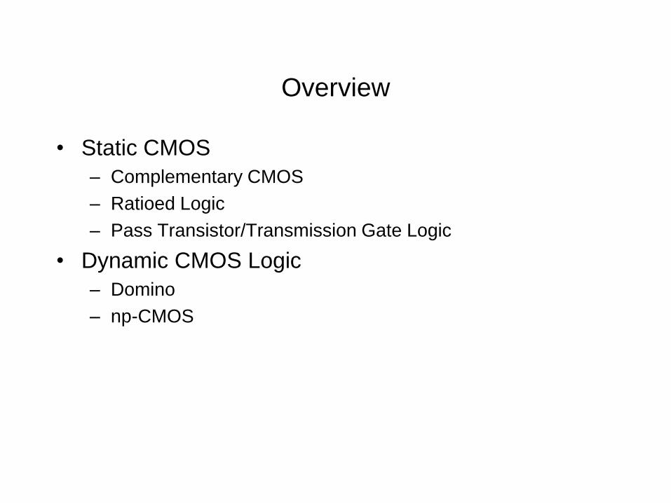
Overview
• Static CMOS
– Complementary CMOS
– Ratioed Logic
– Pass Transistor/Transmission Gate Logic
• Dynamic CMOS Logic
– Domino
– np-CMOS
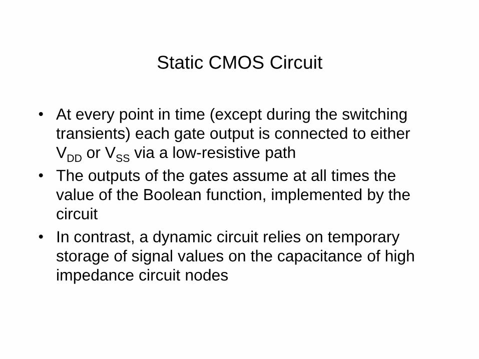
Static CMOS Circuit
• At every point in time (except during the switching
transients) each gate output is connected to either
VDD or VSS via a low-resistive path
• The outputs of the gates assume at all times the
value of the Boolean function, implemented by the
circuit
• In contrast, a dynamic circuit relies on temporary
storage of signal values on the capacitance of high
impedance circuit nodes
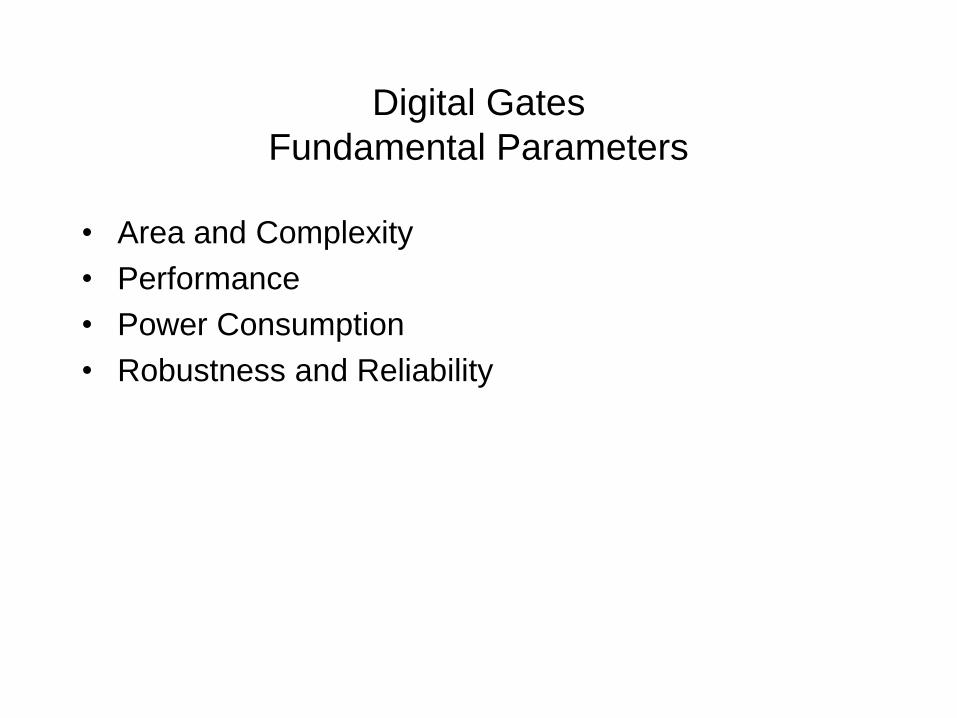
Digital Gates
Fundamental Parameters
• Area and Complexity
• Performance
• Power Consumption
• Robustness and Reliability

What Can Go Wrong in CMOS Logic?
• Incorrect or insufficient power supplies
• Power supply noise
• Noise on gate input
• Faulty connections between transistors
• Clock frequency too high or circuit too slow
Complementary CMOS is pretty
safe against these

How about Ratioed or Dynamic Logic?
• All the previous and
• Incorrect ratios in ratioed logic
• Charge sharing in dynamic logic
• Incorrect clocking in dynamic logic
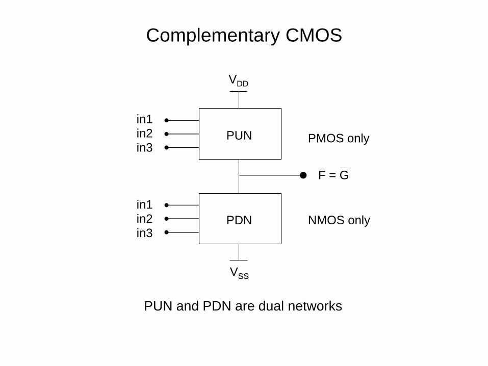
Complementary CMOS
PUN
PDN
in1in2in3
in1in2in3
VDD
VSS
F = G
NMOS only
PMOS only
PUN and PDN are dual networks

NMOS Transistors in Series/Parallel Connection
• Transistors can be thought as a switch controlled by
its gate signal
• NMOS switch closes when switch control input is
high
X Y
A B
X = Y if A = 1 and B = 1, i.e., AB = 1
• NMOS passes a strong 0 but a weak 1
X Y
A
BX = Y if A = 1 or B = 1, i.e., A + B = 1

NMOS Transistors in Series/Parallel Connection
• Connect Y to GND
X Y
A B
X = 0 if A = 1 and B = 1, i.e., A.B = 1
• Implement the complement of PDN
X Y
A
BX = 0 if A = 1 or B = 1, i.e., A + B = 1
X = A.B
X = A + B

PMOS Transistors in Series/Parallel Connection
• PMOS switch closes when switch control input is low
X Y
A B X = Y if A = 0 and B = 0
or A + B = 1
or A.B = 1
• PMOS passes a strong 1 but a weak 0
X Y
A
B X = Y if A = 0 or B = 0
A.B = 1
A + B = 1
PMOS Transistors in Series/Parallel Connection
• Connect Y to VDD
X Y
A B
X = 1 if A = 0 and B = 0
• Combine series PDN and parallel PUN or parallel
PDN and series PUN to complete the logic design to
output good 1 and 0
X Y
A
BX = 1 if A = 0 or B = 0
X = A + B = A.B
X = A.B = A + B

Complementary CMOS Logic Style Construction
• PUN is the DUAL of PDN (can be shown using
DeMorgan’s Theorems)
BABA
BAAB
• The complementary gate is inverting
– Implements NAND, NOR, …
– Non-inverting boolean function needs an inverter
,...),,(,...),,( 321321 inininFinininG

The NAND Circuit
B
A
BA
1 1
1 0
0 1
0
1
A
B
B
Out
A
BA.
,...),,(,...),,( 321321 inininFinininG
BAG .:GND toconnected PDN
ABBAFVDD : toconnected PUN

B
A
1 0
0 0
0 1
0
1
A
B
A B
The NOR Circuit
A + B
A . B
BA Output

Example Gate: COMPLEX CMOS GATE
VDD
A
B
C
D
D
A
B C
OUT = D + A• (B+C)
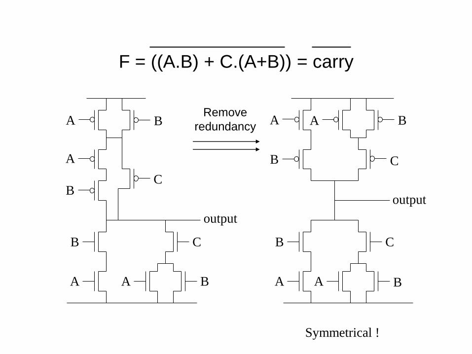
F = ((A.B) + C.(A+B)) = carry
B
C
A
A
output
A
B
B
B
C
A
A
B
B
output
A B
C
A
BA
C
Symmetrical !
Remove
redundancy

F = (ABC+ABC+ABC+ABC) = sum
A
-B
-A
B
-C
-A
-B
A
B
C
C -C
B
A
-B
-A
-B
A
B
-A
output

Full Adder Circuit
A
B
B
C
A
B
CB
A A
A B C A
A B C
B
C
C
B
A
-sum-carry
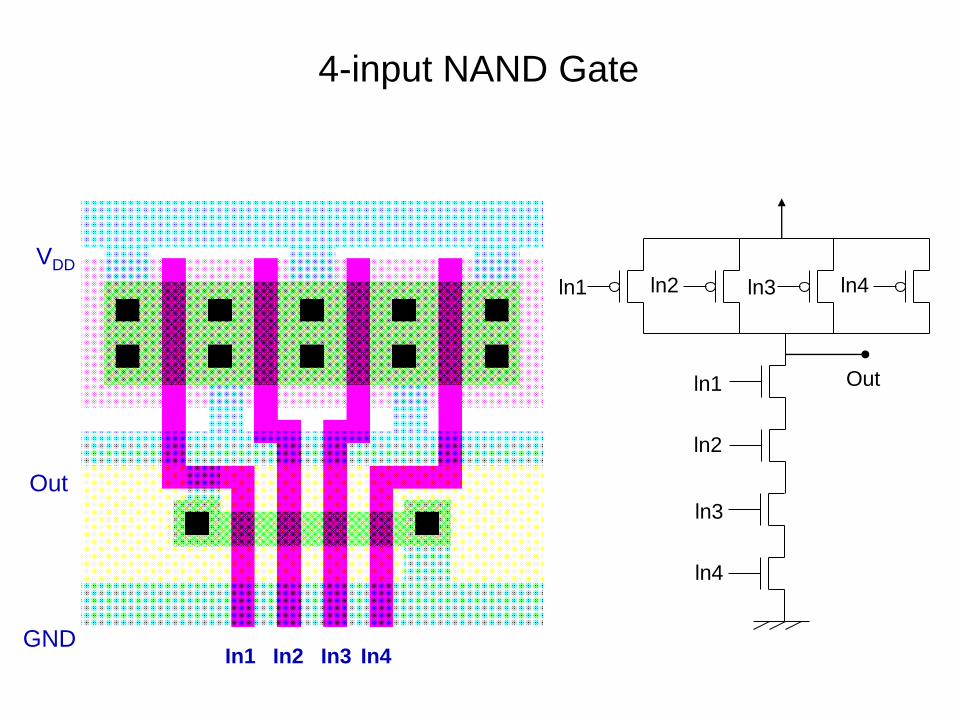
4-input NAND Gate
In1 In2 In3 In4
VDD
GND
Out
ln2
ln1
ln2
Out
ln1
ln4
ln3
ln4ln3
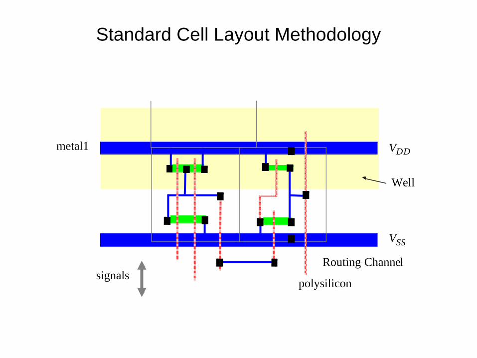
Standard Cell Layout Methodology
VDD
VSS
Well
signalsRouting Channel
metal1
polysilicon

Two Versions of (a+b).c
a c b a b c
xx
GND
VDDVDD
GND
(a) Input order {a c b} (b) Input order {a b c}
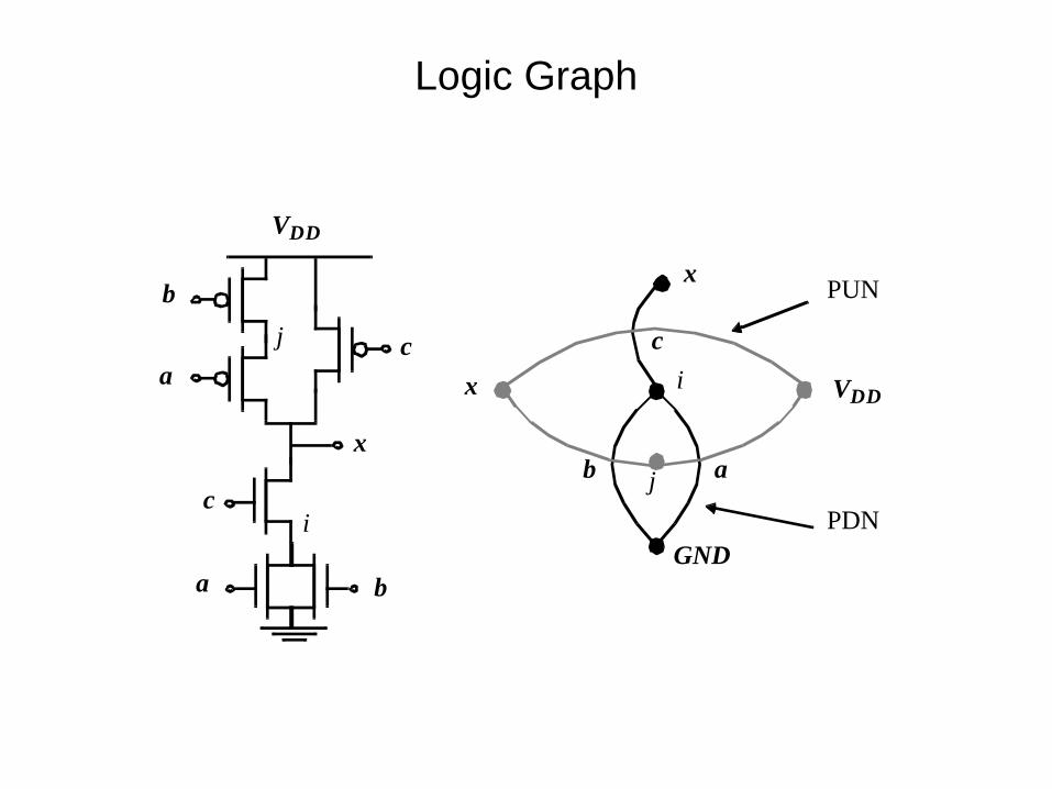
Logic Graph
VDD
c
a
x
b
ca
b
GND
x
VDDx
c
b a
i
j
i
j
PDN
PUN

Consistent Euler Path
{a b c}
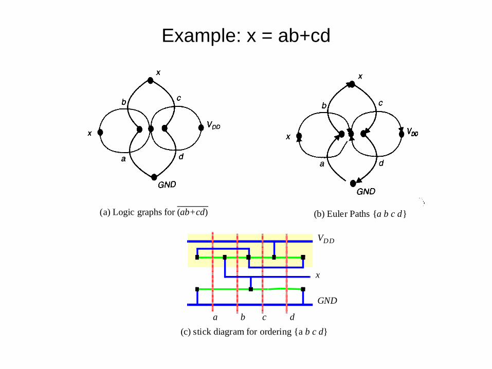
Example: x = ab+cd
GND
x
a
b c
d
VDDx
GND
x
a
b c
d
VDDx
(a) Logic graphs for (ab+cd) (b) Euler Paths {a b c d}
a c d
x
VDD
GND
(c) stick diagram for ordering {a b c d}
b
Properties of Complementary CMOS Gates
• High noise margin
– VOH and VOL are at VDD and GND, respectively
• No static power consumption
– In steady state, no direct path between VDD and VSS
• Comparable rise and fall times under appropriate
scaling of PMOS and NMOS transistors

Transistor Sizing
• For symmetrical response (dc, ac)
• For performance
• Input dependent
• Focus on worst-case

Propagation Delay Analysis - The Switch Model
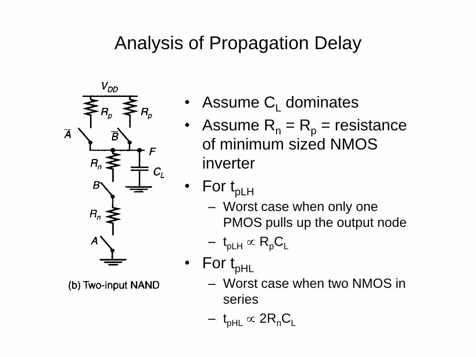
Analysis of Propagation Delay
• Assume CL dominates
• Assume Rn = Rp = resistance
of minimum sized NMOS
inverter
• For tpLH
– Worst case when only one
PMOS pulls up the output node
– tpLH RpCL
• For tpHL
– Worst case when two NMOS in
series
– tpHL 2RnCL

3-Input NAND Gate
inc out
inb
ina
rise-time: 1 transistor (simple)
fall-time: 3 transistor in series
for linear approximation: take 3xRon
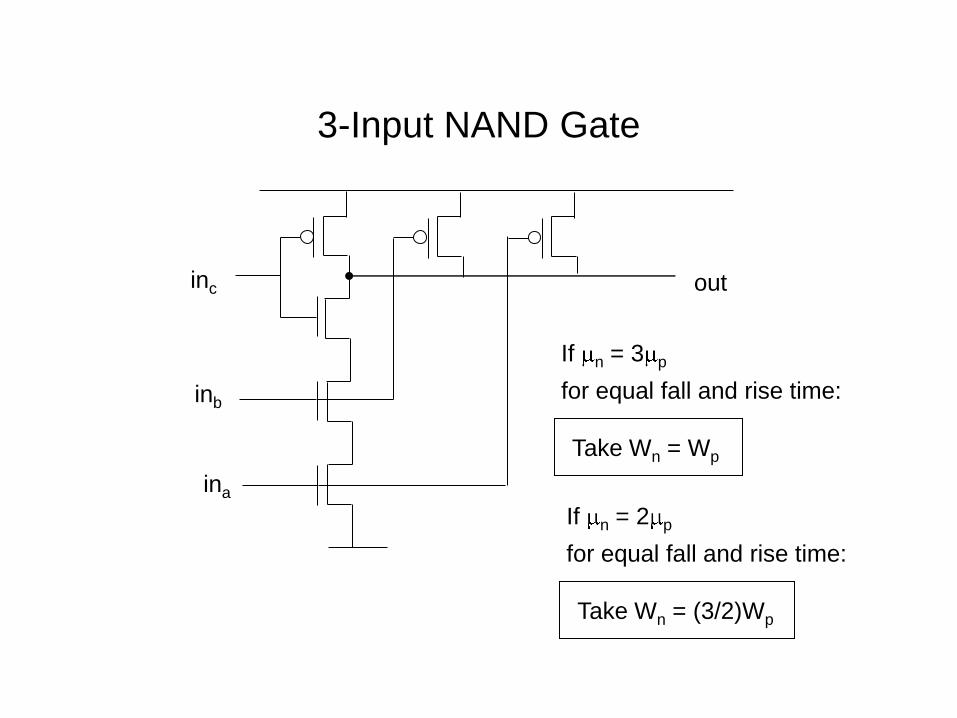
3-Input NAND Gate
inc out
inb
ina
If n = 3 p
for equal fall and rise time:
Take Wn = Wp
If n = 2 p
for equal fall and rise time:
Take Wn = (3/2)Wp

Design for Worst Case

3-input NAND Gate with Parasitic Capacitors
inc
out
inb
ina
Cp+load
Ca
Cb
Cc
P1 P2 P3
N3
N2
N1
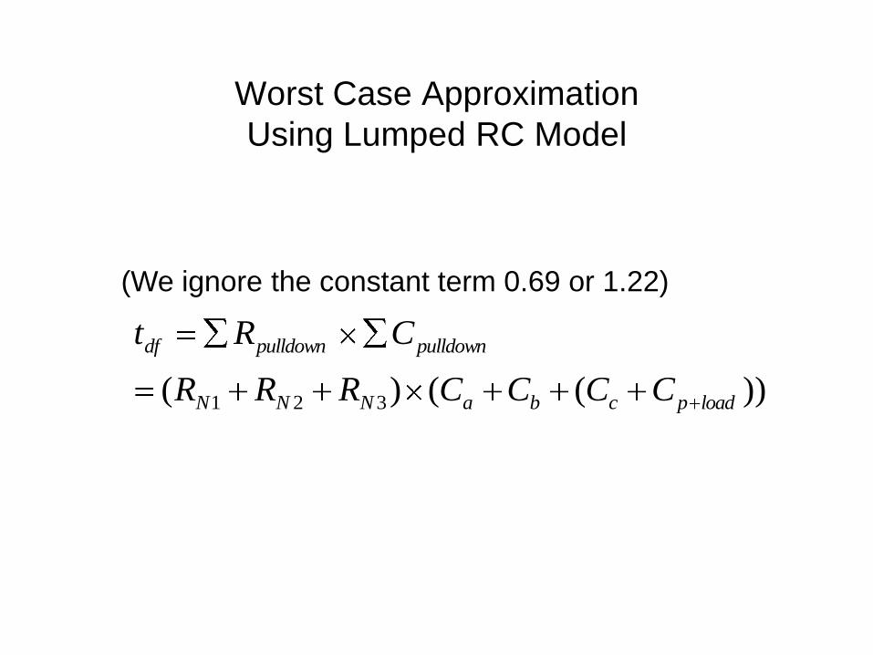
Worst Case Approximation
Using Lumped RC Model
))(()( 321 loadpcbaNNN
pulldownpulldowndf
CCCCRRR
CRt
(We ignore the constant term 0.69 or 1.22)
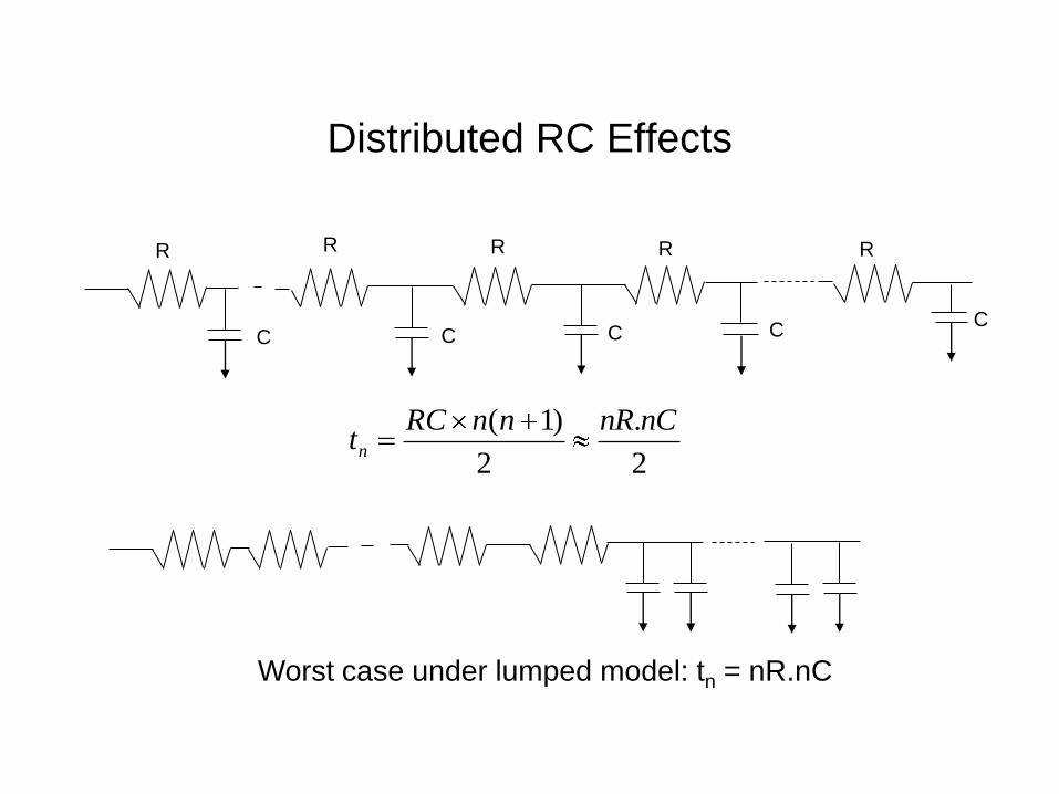
Distributed RC Effects
C C C CC
R R R R R
2
.
2
)1( nCnRnnRCtn
Worst case under lumped model: tn = nR.nC

Comparison
tdf = [RNICa] + [(RN1+RN2)Cb] + [(RN1+RN2+RN3)Cc] +
[(RN1 + RN2 + RN3)Cp+load]
RNC n(n+1)/2 + [(RN1+RN2+RN3)Cp+load]
With RN1 = RN2 = RN3 = RN
and Ca = Cb = Cc = C
n transistors in series
RP-Model
Lumped-Model
RNC n2+ [(RN1+RN2+RN3)Cp+load]

Macro Modeling
td = [RN1Ca] + [(RN1+RN2)Cb] + [(RN1 + RN2 + RN3)Cc] +
[(RN1 + RN2 + RN3)Cp + [(RN1 + RN2 + RN3)Cload]
Internal delay External load
td = Td, internal + x Cload

Effect of Loading
CL = 0.0pF
CL = 0.5pF
CL = 1.0pF
t
td = td, internal + x Cload
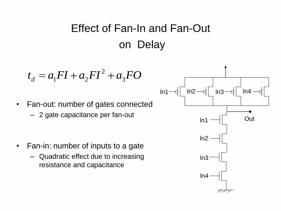
Effect of Fan-In and Fan-Out
on Delay
ln2
ln1
ln2
Out
ln1
ln4
ln3
ln4ln3
• Fan-out: number of gates connected
– 2 gate capacitance per fan-out
• Fan-in: number of inputs to a gate
– Quadratic effect due to increasing
resistance and capacitance
FOaFIaFIatd 3
2
21

tp as a function of Fan-In
1 3 5 7 9fan-in
0.0
1.0
2.0
3.0
4.0t p
(nsec)
tpHL
tp
tpLHlinear
quadratic
AVOID LARGE FAN-IN GATES! (Typically not more than FI < 4)

Example
3-Input NAND gate with Parasitic Capacitors
inc
out
inb
ina
Cp+load
Ca
Cb
Cc
P1 P2 P3
Rn=0.5Rp=
Ca=Cb=Cc=Cj=0.05pF
Cp=3Cj=0.15pF
Cload=2Cg=0.20pF
4102
1

Worst Case Approximation
by Lumped Model
tdr = Rp x (Cc + Cp+load) = 10000 x 0.4 10-12 = 4.0ns
tdf = Rpulldown x Cpulldown
= (RN1 + RN2 + RN3) x (Ca + Cb + (Cc + Cp+load))
= (3 x 5000) x (3 x 0.05 + 0.15 + 0.20) x 10-12
= 7.5ns

Penfield-Rubenstein Model
tdr = Rp x (Cc + Cp+load) = 10000 x 0.4 10-12 = 4.0ns
tdf = [RN1Ca] + [(RN1 + RN2)Cb] + [(RN1 + RN2 + RN3)(Cc + Cp+load)]
= 5000 x 0.05pF + 10000 x 0.05pF + 15000 x 0.4pF = 6.75ns

Worst Case Approximation
by Lumped Model
tdr = Rp x (Cc + Cp+load) = 10000 x 0.45 10-12 = 4.5ns
tdf = Rpulldown x Cpulldown
= (RN1 + RN2 + RN3) x (Ca + Cb + (Cc + Cp+load))
= (3 x 2500) x (3 x 0.10 + 0.15 + 0.20) x 10-12
= 4.875ns
Make Wn = 2Wp

Penfield-Rubenstein Model
tdr = Rp x (Cc + Cp+load) = 10000 x 0.45 10-12 = 4.5ns
tdf = [RN1Ca] + [(RN1 + RN2)Cb] + [(RN1 + RN2 + RN3)(Cc + Cp+load)]
= 2500 x 0.10pF + 5000 x 0.10pF + 7500 x 0.45pF = 4.125ns
Make Wn = 2Wp
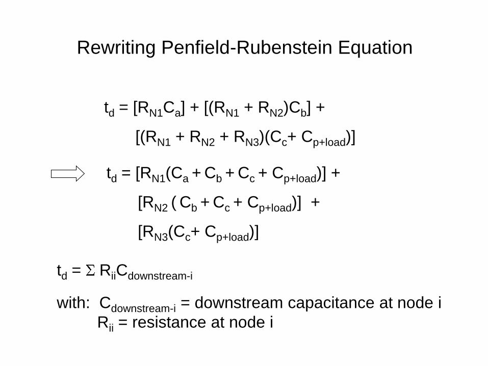
Rewriting Penfield-Rubenstein Equation
td = RiiCdownstream-i
with: Cdownstream-i = downstream capacitance at node i
Rii = resistance at node i
td = [RN1Ca] + [(RN1 + RN2)Cb] +
[(RN1 + RN2 + RN3)(Cc+ Cp+load)]
td = [RN1(Ca + Cb + Cc + Cp+load)] +
[RN2 ( Cb + Cc + Cp+load)] +
[RN3(Cc+ Cp+load)]
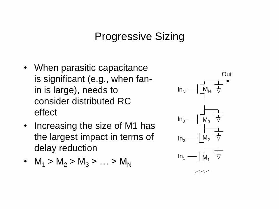
Progressive Sizing
• When parasitic capacitance
is significant (e.g., when fan-
in is large), needs to
consider distributed RC
effect
• Increasing the size of M1 has
the largest impact in terms of
delay reduction
• M1 > M2 > M3 > … > MN
ln3
lnN
Out
ln1
ln2
M1
M2
M3
MN

Delay Optimization by Transistor Ordering
ln3
lnN
Out
ln1
ln2
M1
M2
M3
MN
Critical signal next to supply
Critical path
ln3
lnN
Out
ln1
ln2
M1
M2
M3
MN
Critical signal next to output
Critical path