Combinational Logic Design Principles - UPTstaff.cs.upt.ro/~todinca/DL/Lectures/dl2.pdf ·...
51
Combinational Logic Design Principles Switching algebra Doru Todinca Department of Computers and Information Technology Politehnica University of Timisoara
Transcript of Combinational Logic Design Principles - UPTstaff.cs.upt.ro/~todinca/DL/Lectures/dl2.pdf ·...

Combinational Logic Design PrinciplesSwitching algebra
Doru Todinca
Department of Computers and Information TechnologyPolitehnica University of Timisoara

Outline
Introduction
Switching algebraAxioms of switching algebraTheorems of switching algebraDualityStandard Representation of Logic Functions

Outline
Introduction
Switching algebraAxioms of switching algebraTheorems of switching algebraDualityStandard Representation of Logic Functions
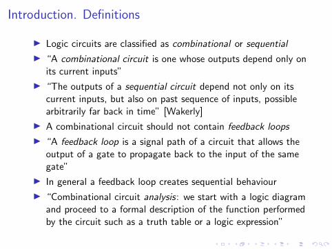
Introduction. Definitions
I Logic circuits are classified as combinational or sequential
I “A combinational circuit is one whose outputs depend only onits current inputs”
I “The outputs of a sequential circuit depend not only on itscurrent inputs, but also on past sequence of inputs, possiblearbitrarily far back in time” [Wakerly]
I A combinational circuit should not contain feedback loops
I “A feedback loop is a signal path of a circuit that allows theoutput of a gate to propagate back to the input of the samegate”
I In general a feedback loop creates sequential behaviour
I “Combinational circuit analysis: we start with a logic diagramand proceed to a formal description of the function performedby the circuit such as a truth table or a logic expression”

Definitions
I Synthesis is the opposite process, where we start with aformal description and obtain a logic diagram
I Logic design starts with an informal description of the circuit(in words), from which we obtain first a formal descriptionand at the end the logic diagram
I Hence, logic design includes synthesis
I Usually the most difficult and creative part is to obtain aformal description from the informal description
I Once we have the formal description we can use tools forsynthesis, in order to obtain the logic diagram for a targettechnology (e.g. FPGA, ASIC, etc)
I Combinational circuits can have more than one output, but inthis chapter we discuss only techniques that apply tocombinational circuits with one output

Outline
Introduction
Switching algebraAxioms of switching algebraTheorems of switching algebraDualityStandard Representation of Logic Functions

Boolean algebra
I Boolean, or switching algebra, deals with two truth values:FALSE and TRUE, or 0 and 1, or LOW and HIGH (signalvoltages)
I Created by George Boole in 1854
I Claude Shannon (1938): adapted the Boolean algebra toswitching circuits (relays at that time):
I A variable expresses the condition of a switching device: closed(1) or open (0)
I Positive logic convention: we associate logic 0 to LOW signalvalues and logic 1 to HIGH signal values
I Negative logic convention: we associate logic 0 to HIGHvalues and logic 1 to LOW values (seldom used)
I The choice of positive or negative convention does not affectthe results of boolean algebra
I We will use this when we will talk about duality

Switching algebra
I A variable denotes the value of a signal: X, Y1, Input1, etc
I A literal is a logic variable or its complement: X, X’, Y1’, etcI An expression combines
I literalsI logic operators: AND (·), OR (+), complementation ( ’)I and parenthesis
I Examples of logic expressions:I (X ′ + Y 1) ·WI ((Y + Z1′) · CS L) · RESET ′
I An equation has the form: variable = expressionI Examples:
I P = (A · B + (C · D))′ + Z1I ((Y + Z1′) · CS L) · RESET ′ = Q0

Outline
Introduction
Switching algebraAxioms of switching algebraTheorems of switching algebraDualityStandard Representation of Logic Functions

Axioms of switching algebra
Axioms, or postulates, are a minimal set of definitions andrelations that we assume to be true, and from which we can deriveall other relations and informations of a mathematical system
(A1) X = 0 if X 6= 1 (A1’) X = 1 if X 6= 0(A2) If X = 0, then X ′ = 1 (A2’) If X = 1, then X ′ = 0(A3) 0 · 0 = 0 (A3’) 1 + 1 = 1(A4) 1 · 1 = 1 (A4’) 0 + 0 = 0(A5) 0 · 1 = 1 · 0 = 0 (A5’) 1 + 0 = 0 + 1 = 1
Table 1: Axioms of switching algebra

Axioms of switching algebra
I Axioms (A1) and (A1’) formalize the fact that a booleanvariable can take only two values: 0 and 1
I Axioms (A2) and (A2’) describe the inverting operator (NOT,denoted also ’)I The symbol for an inverter with input X and output Y and its
algebraic notation Y = X ′ are given in figure 1I X ′ is an expression, and Y = X ′ is an equation
I Axioms (A3)-(A5) describe formally the AND operator, orlogical multiplication, with the symbol multiplication dot (·)
I Axioms (A3’)-(A5’) describe formally the OR operator, orlogical addition, symbolized by a plus sign (+)
I In a logical expression, multiplication has precedence overaddition
I The symbols for AND and OR gates and their algebraicequations are given in figure 2 (a) and (b)
I The five pairs of axioms (A1-A5) and (A1’-A5’) completelycharacterize switching algebra
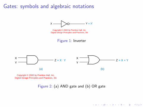
Gates: symbols and algebraic notations
X Y = X′
Copyright © 2000 by Prentice Hall, Inc. Digital Design Principles and Practices, 3/e
Figure 1: Inverter
X
YZ = X • Y
X
YZ = X + Y
(a) (b)
Copyright © 2000 by Prentice Hall, Inc. Digital Design Principles and Practices, 3/e
Figure 2: (a) AND gate and (b) OR gate
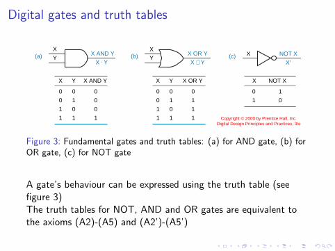
Digital gates and truth tables
(c)
X NOT X
1
0 1
0
NOT XX(a)
X
0
1
X AND YY
0
1
1
0
1
0
0
0
0
1
X AND YX
Y (b)
X
0
1
X OR YY
0
1
1
0
1
0
0
1
1
1
X OR Y
X′ X • Y X + Y
X
Y
Copyright © 2000 by Prentice Hall, Inc. Digital Design Principles and Practices, 3/e
Figure 3: Fundamental gates and truth tables: (a) for AND gate, (b) forOR gate, (c) for NOT gate
A gate’s behaviour can be expressed using the truth table (seefigure 3)The truth tables for NOT, AND and OR gates are equivalent tothe axioms (A2)-(A5) and (A2’)-(A5’)
Outline
Introduction
Switching algebraAxioms of switching algebraTheorems of switching algebraDualityStandard Representation of Logic Functions

Theorems of switching algebra
I Switching algebra theorems are statements that are alwaystrue and that can be obtained from axioms
I The theorems are very useful for simplifying algebraicexpressions used for analysis and synthesis of combinationaldevices
I Most theorems can be proved by induction: either perfectinduction or finite inductionI Perfect induction means to prove that the theorem is true for
all possible casesI Finite induction means to prove that the theorem is true for
n = 2 (the basis step) and that, if the theorem is true forn = i , then it is true for n = i + 1 (induction step)
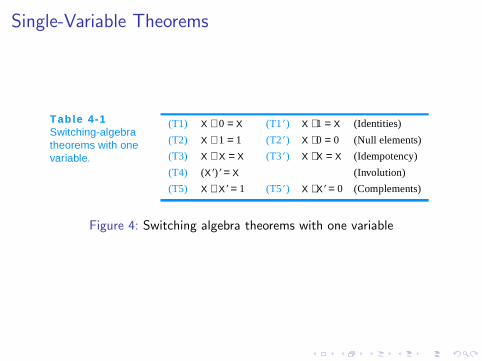
Single-Variable Theorems
Table 4-1Switching-algebra theorems with one variable.
(T1) X + 0 = X (T1′ ) X ⋅ 1 = X (Identities)
(T2) X + 1 = 1 (T2′ ) X ⋅ 0 = 0 (Null elements)
(T3) X + X = X (T3′ ) X ⋅ X = X (Idempotency)
(T4) (X′ )′ = X (Involution)
(T5) X + X′ = 1 (T5′ ) X ⋅ X′ = 0 (Complements)
Figure 4: Switching algebra theorems with one variable

Single-Variable Theorems
I Single variable theorems allow us to simplify algebraicexpression:I For example, to replace X + 0 with X , X + 1 with 1, X + X
with XI Or, to replace X · 1 with X , X · 0 with 0, X · X with X
I All can be proved by perfect inductionI Proof of (T1). We can have two situations, because X can
have only two values (according to A1 and A1’):
1. If X = 0 (T1) becomes 0 + 0 = 0, which is true, according to(A4’)
2. If X = 1 (T1) becomes 1 + 0 = 1, true, according to (A5’)
I All single variable theorems can be proved in a similar way (atthe lab !)

Two- and Three-Variable Theorems
Table 4-2 Switching-algebra theorems with two or three variables.
(T6) X + Y = Y + X (T6′ ) X ⋅ Y = Y ⋅ X (Commutativity)
(T7) (X + Y) + Z = X + (Y + Z) (T7′ ) (X ⋅ Y) ⋅ Z = X ⋅ (Y ⋅ Z) (Associativity)
(T8) X ⋅ Y + X ⋅ Z = X ⋅ (Y + Z) (T8′ ) (X + Y) ⋅ (X + Z) = X + Y ⋅ Z (Distributivity)
(T9) X + X ⋅ Y = X (T9′ ) X ⋅ (X + Y) = X (Covering)
(T10) X ⋅ Y + X ⋅ Y′ = X (T10′ ) (X + Y) ⋅ (X + Y') = X (Combining)
(T11) X ⋅ Y + X′ ⋅ Z + Y ⋅ Z = X ⋅ Y + X′ ⋅ Z (Consensus)
(T11′ ) (X + Y) ⋅ (X′ + Z) ⋅ (Y + Z) = (X + Y) ⋅ (X′ + Z)
Figure 5: Switching algebra theorems with two and three variable
In all theorems it is possible to replace any variable with anarbitrary logic expression.

Commutativity and Associativity
I Commutativity:I T6 and T6’ indicate that we can change the order of therms in
a logical sum or a logical product
I Associativity:I Without associativity, an expression like W + X + Y + Z or
W · X · Y · Z is ambiguousI theorems T7 and T7’ indicate that parenthesizetion is not
relevant,I so that we can write W + X + Y + Z instead of
(((W + X ) + Y ) + Z ),I or W · X · Y · Z instead of, e.g., (W · X ) · (Y · Z )
I Associativity and commutativity tell us that:I We can extend the · and + operators, that have been defined
as binary operators, to any number of variablesI That means that we can have AND and OR gates with 2, 3, 4,
8, . . . inputsI We may connect the gates’ inputs in any order

Two- and Three-Variable Theorems: Distributivity
I Distributivity:I Theorem T8 looks like distributivity of real and integer number
multiplication over additionI It allows us to “multiply out” expressions in order to obtain a
sum-of-product form:I W · (X + Y + Z ) = W · ((X + Y ) + Z ) =
W · (X + Y ) + W · Z = W · X + W · Y + W · ZI Theorem T8’ does not hold for real (or integer) number
addition and multiplication, but in Boolean algebra, logicaddition is distributive over logic multiplication
I It means that we can “add out” expressions to obtain theproduct-of-sum form:
I W + (X · Y · Z ) = W + (X · (Y · Z )) =(W + X ) · (W + (Y · Z )) = (W + X ) · (W + Y ) · (W + Z )

2- and 3-Variable Theorems: Covering and Combining
I Both covering and combining theorems are used forminimization of logic expressions
I They can be proved by perfect induction, but also using othertheorems, as follows:
X + X · Y = X · 1 + X · Y (according to T1’)= X · (1 + Y ) (according to T8)= X · 1 (according to T2)= X (according to T1’)
Table 2: Proof of covering theorem
X · Y + X · Y ′ = X · (Y + Y ′) (according to T8)= X · 1 (according to T5)= X (according to T1’)
Table 3: Proof of combining theorem
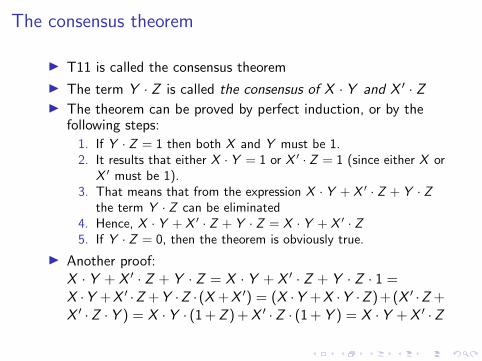
The consensus theorem
I T11 is called the consensus theorem
I The term Y · Z is called the consensus of X · Y and X ′ · ZI The theorem can be proved by perfect induction, or by the
following steps:
1. If Y · Z = 1 then both X and Y must be 1.2. It results that either X · Y = 1 or X ′ · Z = 1 (since either X or
X ′ must be 1).3. That means that from the expression X · Y + X ′ · Z + Y · Z
the term Y · Z can be eliminated4. Hence, X · Y + X ′ · Z + Y · Z = X · Y + X ′ · Z5. If Y · Z = 0, then the theorem is obviously true.
I Another proof:X · Y + X ′ · Z + Y · Z = X · Y + X ′ · Z + Y · Z · 1 =X ·Y +X ′ ·Z +Y ·Z · (X +X ′) = (X ·Y +X ·Y ·Z ) + (X ′ ·Z +X ′ ·Z ·Y ) = X ·Y · (1 +Z ) +X ′ ·Z · (1 +Y ) = X ·Y +X ′ ·Z

n-Variable Theorems
Table 4-3 Switching-algebra theorems with n variables.
(T12)(T12′ )
X + X + … + X = XX ⋅ X ⋅ … ⋅ X = X
(Generalized idempotency)
(T13)(T13′ )
(X1 ⋅ X2 ⋅ … ⋅ Xn)′ = X1′ + X2′+ … + Xn′ (X1 + X2 + … + Xn)′ = X1′ ⋅ X2′ ⋅ … ⋅ Xn′
(DeMorgan's theorems)
(T14) [F(X1,X2, … , Xn, +, ⋅ )]′ = F(X1′ ,X2′ , … ,Xn′ , ⋅ , +) (Generalized DeMorgan's theorem)
(T15)(T15′ )
F(X1,X2, … ,Xn) = X1 ⋅ F(1,X2, … , Xn) + X1′ ⋅ F(0,X2, … ,Xn)
F(X1,X2, … ,Xn) = [X1 + F(0,X2,… ,Xn)] ⋅ [X1′ + F(1,X2, … , Xn)]
(Shannon's expansion theorems)
Figure 6: Switching algebra theorems with n variable
I The theorems are true for an arbitrary number of variables, n.
I Most of them can be proved by finite induction.
I DeMorgan’s theorems T13 and T13’ are probably the mostused theorems from switching algebra.

n-Variable Theorems: proof of T12
I Proof is by finite induction:
I Basis step: for n = 2 the theorem is true, according to T3.
I Induction step: suppose that for n = i T12 is true, i.e.X + X + . . . + X︸ ︷︷ ︸
i
= X
I We will prove T12 for n = i + 1:
X + X + . . . + X︸ ︷︷ ︸i+1
= X + (X + . . . + X︸ ︷︷ ︸i
)
= X + X (n = i)= X (according to T3)
Table 4: Proof of generalized idempotency by finite induction

DeMorgan: T13
I Theorem T13 says that an n-input AND gate with negatedoutput is equivalent with an n-input OR gate with negatedinputs
I Figure 7 (a) and (b) illustrate this, for n = 2
I Figure 7 (c) and (d) show the gates symbols
I In 7 (d) the bubbles on the inputs signify that the gate’sinputs are inverted
I Theorem T13’ says that an n-input OR gate with invertedoutput is equivalent with an n-input AND gate with invertedinputs
I It is illustrated in figure 8 (a) and (b), while (c) and (d)contain the gates symbols

DeMorgan: T13
X
Y
X
Y
X
Y
Z = (X • Y)′ Z = (X • Y)′
X′
Y′
X
Y
Z = X′ + Y′
(a) (c)
(b) Z = X′ + Y′ (d)
X • Y
Copyright © 2000 by Prentice Hall, Inc. Digital Design Principles and Practices, 3/e
Figure 7: Equivalent circuits for NAND gate, according to DeMorgan’stheorem T13

DeMorgan: T13’
X
Y
X
Y
X
Y
Z = (X + Y)′ Z = (X + Y)′
X′
Y′
X
Y
Z = X′ • Y′
(a) (c)
(b) Z = X′ • Y′ (d)
X + Y
Figure 8: Equivalent circuits for NOR gate, according to DeMorgan’stheorem T13’

DeMorgan
I Theorems T13 and T13’ can be proved by finite induction
I The basis step, for n = 2, can be proved by perfect induction
I Theorems T13 and T13’ can be used to prove T14, if wedecompose the arbitrary function F in sum of products, andrespectively product of sums and apply recursively T13 andT13’
I We will use another approach: first demonstrate T14 usingduality, then T13 and T13’ will result as particular cases ofT14
I In T14, the complement (F )′ of a function F is defined asbeing the logic expression whose value is the opposite value ofF, for every possible input combination.

Generalized DeMorgan
I Theorem T14 explains how to complement an n-variable logicexpression:I by swapping + and · and complementing all variables
I As a result, the uncomplemented variables will becomplemented
I And the complemented variables will be uncomplemented(because of theorem T4, involution: (X ′)′ = X )
I Example. Let’s consider the following expression:I F (W ,X ,Y ,Z ) = (W ′ + X ) · (X + Y ) · (W + (X ′ · Z ′))I Applying theorem T14, we will obtain:I [F (W ,X ,Y ,Z )]′ = ((W ′)′·X ′)+(X ′·Y ′)+(W ′·((X ′)′+(Z ′)′))I Using theorem T4 we will have:I [F (W ,X ,Y ,Z )]′ = (W · X ′) + (X ′ · Y ′) + (W ′ · (X + Z ))

Outline
Introduction
Switching algebraAxioms of switching algebraTheorems of switching algebraDualityStandard Representation of Logic Functions

Duality
I All axioms of switching algebra are given in pairs
I The primed version of an axiom is obtained from the unprimedversion by swapping 0 and 1 and, if present, · and +.
I If a theorem can be proved using certain axioms, then theprimed theorem can be also proved (using the primed axioms)
I We can give the following metatheorem
I Principle of duality : Any theorem or identity in switchingalgebra remains true if 0 and 1 are swapped and · and + areswapped too.
I A metatheorem is a theorem about theorems.
I We will formally define the dual of a logic expression

Duality
DefinitionIf F (X1,X2, . . . ,Xn, ·,+,′ ) is a fully parenthesized logic expressioninvolving the variables X1,X2, . . . ,Xn and the operators ·, +, and ′,then the dual of F , written FD , is the same expression with + and· swapped:
FD(X1,X2, , . . .Xn, ·,+,′ ) = F (X1,X2, . . .Xn,+, ·,′ )
Using duality, theorem T14 can be expressed in the following way:
[F (X1,X2, , . . .Xn)]′ = FD(X ′1,X
′2, . . .X
′n)

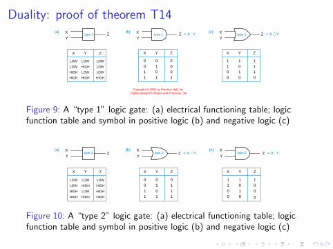
Duality: proof of theorem T14
I Figure 9 (a) shows the electrical function table of a gate thatwe call “type 1” gate
I In positive logic, i.e., if we associate 0 to LOW and 1 toHIGH, it is an AND gate (fig 9 (b))
I But in negative logic (LOW=1 and HIGH=0), “type 1” gateis an OR gate (fig 9 (c))
I In the same way we can consider the “type 2” gate fromfigure 10, which is an OR gate in positive logic and an ANDgate in negative logic
I Obviously, similar tables can be given for gates with anynumber of inputs
Duality: proof of theorem T14
Z = X + Y= X • Y Z
X Y Z
X
YZ
X Y Z
X
Y
LOW LOW LOW 0 0 0 1 1 1LOW HIGH LOW 0 1 0 1 0 1HIGH LOW LOW 1 0 0 0 1 1HIGH HIGHHIGH 1 11 0 00
X Y Z
X
Y
(a)type 1
(b) (c)type 1 type 1
Copyright © 2000 by Prentice Hall, Inc. Digital Design Principles and Practices, 3/e
Figure 9: A “type 1” logic gate: (a) electrical functioning table; logicfunction table and symbol in positive logic (b) and negative logic (c)
= X • YZ(a)
X Y Z
X
YZtype 2
(b)
X Y Z
X
Y
(c)
LOW LOW LOW 0 0 0 1 1 1
LOW HIGH HIGH 0 1 1 1 0 0
HIGH LOW HIGH 1 0 1 0 1 0
0HIGH HIGHHIGH 1 11 0 0
X Y Z
Z = X + YX
Ytype 2 type 2
Figure 10: A “type 2” logic gate: (a) electrical functioning table; logicfunction table and symbol in positive logic (b) and negative logic (c)

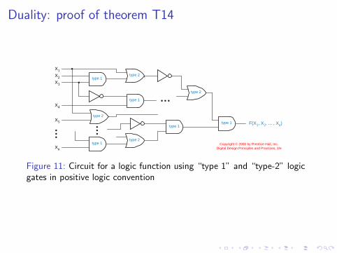
Duality: proof of theorem T14
I Suppose we have an arbitrary logic expressionF (X1,X2, . . . ,Xn)
I We can build a circuit for this logic expression under thepositive logic convention, using inverters (NOT gates) forNOT operations, type 1 gates for AND operations and type 2gates for OR operations
I We will obtain the circuit from figure 11
I Without changing the circuit, we change the logic conventionand use negative logic
I The voltage levels do not change when we change the logicconvention, which means that:I the “type 1” gates will be OR gates and “type 2” gates will be
AND gatesI each input will be replaced by its complementI inverters will remain unchanged
I We will obtain the circuit from figure 12

Duality: proof of theorem T14
I The function realized by the circuit from figure 12 is the dualof function F , realized by the circuit in positive logic (fromfigure 11)
I For each combination of input voltages, the circuit fromfigures 11 and 12 will produce the same voltage
I But, because we use different logic conventions, it means thatthe logic values of the circuit from the two figures will bealways complemented.
I Which means that
F (X1,X2, , . . .Xn) = [FD(X ′1,X
′2, . . .X
′n)]′
I By complementing both sides, we obtain theorem T14.
Duality: proof of theorem T14
X2
X3
X1
X4
X5
Xn
type 1
type 1
type 1
type 1
type 2
type 2
type 2
F(X1, X2, ... , Xn)
type 2
type 1
Copyright © 2000 by Prentice Hall, Inc. Digital Design Principles and Practices, 3/e
Figure 11: Circuit for a logic function using “type 1” and “type-2” logicgates in positive logic convention

Duality: proof of theorem T14
X2′ X3′
X1′
X4′
X5′
Xn′
type 1
type 1
type 1
type 1
type 2
type 2
type 2
type 2
type 1 FD(X1′ , X2′ , ... , Xn′ )
Copyright © 2000 by Prentice Hall, Inc. Digital Design Principles and Practices, 3/e
Figure 12: The circuit from figure 11 under negative logic convention

Outline
Introduction
Switching algebraAxioms of switching algebraTheorems of switching algebraDualityStandard Representation of Logic Functions
Truth table
I The truth table is the most basic representation of a logicfunction of a combinational circuit
I A truth table lists the output of a circuit for all its inputcombinations
I The order in which we list the input combinations istraditionally the ascending binary counting order
I A truth table for a combinational circuit with n inputs has 2n
rows.
I Figure 13 presents the general structure of a truth table for acircuit with 3 inputs (a three-variable truth table)
I With 3 variable a truth table has 23 = 8 rows
I Figure 14 presents a truth table for a particular logic 3-inputlogic function F.

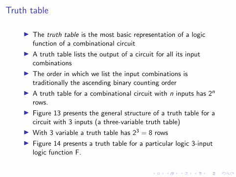
General truth table
Table 4 -4General truth table structure for a 3-variable logic function, F(X,Y, Z).
Row X Y Z F
0 0 0 0 F(0,0,0)
1 0 0 1 F(0,0,1)
2 0 1 0 F(0,1,0)
3 0 1 1 F(0,1,1)
4 1 0 0 F(1,0,0)
5 1 0 1 F(1,0,1)
6 1 1 0 F(1,1,0)
7 1 1 1 F(1,1,1)
Figure 13: General truth table for a 3-variable logic function

Truth table for a particular logic function
Row X Y Z F Table 4-5Truth table for a particular 3-variable logic function, F(X,Y, Z).
0 0 0 0 1
1 0 0 1 0
2 0 1 0 0
3 0 1 1 1
4 1 0 0 1
5 1 0 1 0
6 1 1 0 1
7 1 1 1 1
Figure 14: The truth table for a particular 3-variable logic function

Standard representations of logic functions: Definitions
I A literal is a variable or the complement of a variable.I Examples: X, X’, Y, Y’, RESET.
I A product term is a single literal or a logic product of two ormore literals.I Examples: Z ′, W · X · Y , W · X ′ · Y ′ · Z
I A sum-of-products expression is a logical sum of producttermsI Examples: W · X · Y + W · X ′ · Y ′ + W ′ · X · Y
I A sum term is a single literal or a logical sum of two or moreliterals.I Examples: W + X + Y , W ′ + X ′ + Y ′, W + X + Y ′ + Z ′
I A product-of-sum expression is a logical product of sumterms.I Examples: (W + X + Y ) · (W ′ + X ′ + Y ′) · (W ′ + X + Y ),
Z ′ · (W + X + Y ′ + Z ′)

Standard representations of logic functions: Definitions
I A normal term is a product or sum term in which no variableappears more than once.I A non-normal term can always be simplified to a constant or a
normal term using one of the theorems T3, T3’(idempotency),T5 or T5’ (complements).
I Examples of non-normal terms: W ·X ·X · Z , W ·X ′ ·Y ′ ·W ′,W + W + X + Y , W + W ′ + Y + Z
I Examples of normal terms: W · X ′ · Y ′ · Z , W · X · Y ′ · Z ,W + X + Y + Z ′, W ′ + X ′ + Y + Z
I An n-variable minterm is a normal product term of n literals.I There are 2n such product terms.I Examples of 3-variable minterms: W · X · Y , W ′ · X · Y ′,
W ′ · X ′ · Y ′
I Examples of 4-variable minterms: W · X · Y · Z ,W ′ · X ′ · Y ′ · Z , W ′ · X ′ · Y ′ · Z ′
I An n-variable maxterm is a normal sum term of n literals.I Examples of 4-variable maxterms: W + X + Y + Z ,
W ′ + X ′ + Y ′ + Z , W ′ + X ′ + Y ′ + Z ′
Minterms, maxterms and truth tables
I In an n-variable minterm (or maxterm), each variable appearsexactly once, in either uncomplemented or complemented form
I There is a close correspondence between the truth table andminterms and maxterms.
I A minterm can be defined as a product term that is 1 inexactly one row of the truth table
I A maxterm can be defined as a sum term that is 0 in exactlyone row of the truth table
I In figure 15 we can see this correspondence for a 3-variabletruth table.
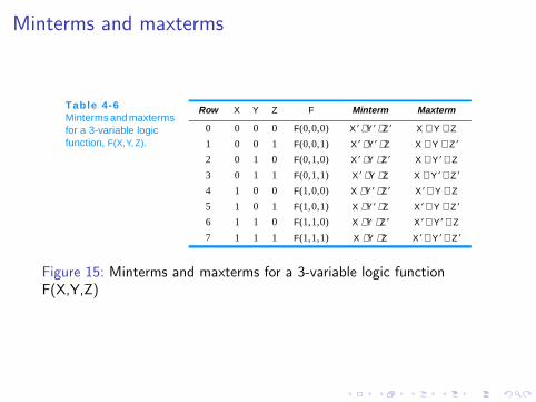
Minterms and maxterms
Table 4-6Minterms and maxterms for a 3-variable logic function, F(X,Y, Z).
Row X Y Z F Minterm Maxterm
0 0 0 0 F(0,0,0) X′ ⋅ Y′ ⋅ Z′ X + Y + Z1 0 0 1 F(0,0,1) X′ ⋅ Y′ ⋅ Z X + Y + Z′ 2 0 1 0 F(0,1,0) X′ ⋅ Y ⋅ Z′ X + Y′ + Z3 0 1 1 F(0,1,1) X′ ⋅ Y ⋅ Z X + Y′ + Z′ 4 1 0 0 F(1,0,0) X ⋅ Y′ ⋅ Z′ X′ + Y + Z5 1 0 1 F(1,0,1) X ⋅ Y′ ⋅ Z X′ + Y + Z′ 6 1 1 0 F(1,1,0) X ⋅ Y ⋅ Z′ X′ + Y′ + Z7 1 1 1 F(1,1,1) X ⋅ Y ⋅ Z X′ + Y′ + Z′
Figure 15: Minterms and maxterms for a 3-variable logic functionF(X,Y,Z)

Minterm and maxterm number
I An n-variable minterm can be represented by an n-bit integer,named the minterm number
I The name minterm i will denote the minterm correspondingto row i of the truth table
I In minterm i , a particular variable appears complemented ifthe corresponding bit in the binary representation of i is 0,and uncomplemented, if the corresponding bit in the binaryrepresentation of number i is 1.
I Example:I the minterm 5 corresponds to row 5 in table 4-5 from figure 15I the binary representation of number 5 on 3 bits is 101I The corresponding minterm will be X · Y ′ · Z
I In maxterm i a variable is complemented if the correspondingbit in the binary representation of number i is 1 anduncomplemented if that corresponding bit is 0I Example: maxterm 5 is X ′ + Y + Z ′

Canonical sum, minterm list
I The canonical sum of a logic function is the sum of theminterms corresponding to truth-table rows (inputcombinations) for which the function is 1
I Example: for the table 4-5 (from figure 14) the canonical sumis: F =
∑X ,Y ,Z (0, 3, 4, 6, 7) =
X ′ · Y ′ · Z ′ + X ′ · Y · Z + X · Y ′ · Z ′ + X · Y · Z ′ + X · Y · ZI The notation
∑X ,Y ,Z (0, 3, 4, 6, 7) is a minterm list, meaning
“the sum of minterms 0, 3, 4, 6 and 7 with variables X , Y ,and Z ”
I The minterm list is called also the on-set of the logic functionbecause each minterm “turns on” the output for exactly oneinput combination.
I Any logic function can be written as a canonical sum.

Canonical product, maxterm list
I The canonical product of a logic function is a product of themaxterms corresponding to input combinations for which thefunction produces a 0 output.
I Example: the canonical product for the logic function in Table4-5 from figure 14 is:F =
∏X ,Y ,Z (1, 2, 5) = (X+Y +Z ′)·(X+Y ′+Z )·(X ′+Y +Z ′)
I The notation∏
X ,Y ,Z (1, 2, 5) is a maxterm list and means“the product of maxterms 1, 2, and 5 with variables X , Y ,and Z”
I The maxterm list is known also as the off-set for the logicfunction because each maxterm “turns off” the function forexactly one input combination.
I Any logical function can be written as a canonical product.

Minterm list and maxterm list
I For a function of n variables, the possible minterm andmaxterm numbers are in the set {0, 1, . . . , 2n − 1}
I A minterm list or a maxterm list contain a subset of thesenumbers
I The minterm list and the maxterm list are complemented
I Hence, in order to switch from minterm list to maxterm list(or vice-versa), take the set complemented.
I Examples:I
∑A,B,C (0, 1, 2, 3) =
∏A,B,C (4, 5, 6, 7)
I∑
X ,Y (1) =∏
X ,Y (0, 2, 3)I
∑W ,X ,Y ,Z (0, 1, 2, 3, 5, 7, 11, 13) =∏W ,X ,Y ,Z (4, 6, 8, 9, 10, 12, 14, 15)

Possible representations for a combinational logic function
1. A truth table
2. An algebraic sum of minterms, the canonical sum
3. A minterm list using the∑
notation
4. An algebraic product of maxterms, the canonical product
5. A maxterm list using the∏
notation.
All representations are equivalent. Given one of them, we canobtain all others.