COMBINATIONAL LOGIC DESIGNtestbankcollege.eu/sample/Solution-Manual-Digital-Design...Full file at 14...
28
13 CHAPTER 2 COMBINATIONAL LOGIC DESIGN 2.1 EXERCISES Any problem noted with an asterisk (*) represents an especially challenging problem. Section 2.2: Switches 2.1. A microprocessor in 1980 used about 10,000 transistors. How many of those micro- processors would fit in a modern chip having 3 billion transistors? 3,000,000,000 / 10,000 = 300,000 microprocessors 2.2 The first Pentium microprocessor had about 3 million transistors. How many of those microprocessors would fit in a modern chip having 3 billion transistors? 3,000,000,000 / 3,000,000 = 1,000 microprocessors 2.3 Describe the concept known as Moore’s Law. Integrated circuit density doubles approximately every 18 months. 2.4 Assume for a particular year that a particular size chip using state-of-the-art technol- ogy can contain 1 billion transistors. Assuming Moore’s Law holds, how many tran- sistors will the same size chip be able to contain in ten years? Approximately 100 billion transistors (10 years * 12 months/year / 18 months/dou- bling = 6.667 doublings. 1 billion * 2 6.667 = 101.617 billion). 2.5 Assume a cell phone contains 50 million transistors. How big would such a cell phone be if the phone used vacuum tubes instead of transistors, assuming a vacuum tube has an volume of 1 cubic inch? 50,000,000 transistors * 1 in 3 /transistor = 50,000,000 in 3 (nearly 30,000 cubic feet - as large as a house) ://TestbankCollege.eu/Solution-Manual-Digital-Design-with-RTL-Design-Verilog-and-VHDL-2nd-Edition-Vahi
Transcript of COMBINATIONAL LOGIC DESIGNtestbankcollege.eu/sample/Solution-Manual-Digital-Design...Full file at 14...

13
CHAPTER 2
COMBINATIONAL LOGIC DESIGN
2.1 EXERCISES Any problem noted with an asterisk (*) represents an especially challenging problem.
Section 2.2: Switches
2.1. A microprocessor in 1980 used about 10,000 transistors. How many of those micro-processors would fit in a modern chip having 3 billion transistors?3,000,000,000 / 10,000 = 300,000 microprocessors
2.2 The first Pentium microprocessor had about 3 million transistors. How many ofthose microprocessors would fit in a modern chip having 3 billion transistors?3,000,000,000 / 3,000,000 = 1,000 microprocessors
2.3 Describe the concept known as Moore’s Law.Integrated circuit density doubles approximately every 18 months.
2.4 Assume for a particular year that a particular size chip using state-of-the-art technol-ogy can contain 1 billion transistors. Assuming Moore’s Law holds, how many tran-sistors will the same size chip be able to contain in ten years? Approximately 100 billion transistors (10 years * 12 months/year / 18 months/dou-bling = 6.667 doublings. 1 billion * 26.667 = 101.617 billion).
2.5 Assume a cell phone contains 50 million transistors. How big would such a cellphone be if the phone used vacuum tubes instead of transistors, assuming a vacuumtube has an volume of 1 cubic inch?50,000,000 transistors * 1 in3/transistor = 50,000,000 in3 (nearly 30,000 cubic feet -as large as a house)
Full file at http://TestbankCollege.eu/Solution-Manual-Digital-Design-with-RTL-Design-Verilog-and-VHDL-2nd-Edition-Vahi

14 c 2 Combinational Logic Design
2.6 A modern desktop processor may contain 1 billion transistors in a chip area of 100mm2. If Moore’s Law continues to apply, what would be chip area for those 1 billiontransistors after 9 years? What percentage is that area of the original area? Name aproduct into which the smaller chip might fit whereas the original chip would havebeen too big.Doubling chip capacity every 18 months also suggests halving of size every 18months of the same number of transistors. 9 years / 18 months is 108 months / 18months = 6 halvings. 100 mm2 * (1/2)6 = 100 mm2 / 64 = 1.56 mm2 . 1.56 mm2 /100 mm2 = 1.56% of the original area. A product into which such a small chip mightnow fit is a hearing aid, for example.
Section 2.3: The CMOS Transistor
2.7 Describe the behavior of the CMOS transistorcircuit shown in Figure 2.77, clearly indicatingwhen the transistor circuit conducts.When x is a logical 0, the top transistor will con-duct, otherwise the top transistor will not con-duct. Likewise, when y is a logical 0, the bottomtransistor will conduct and not conduct other-wise. Thus, the circuit conducts only when x is 0and y is 0.
2.8 If we apply a voltage to the gate of a CMOS transistor, why doesn’t the current flowto the transistor’s source or drain?An insulator exists between the gate and the source-drain channel, prohibiting cur-rent from flowing to the transistor’s source or drain.
2.9 Why does applying a positive voltage to the gate of a CMOS transistor cause thetransistor to conduct between source and drain?The positive voltage at the gate attracts electrons into the channel between sourceand drain. Those electrons are enough to change the channel from non-conducting toconducting.
Section 2.4: Boolean Logic Gates—Building Blocks for Digital Circuits
2.10 Which Boolean operation, AND, OR or NOT, is appropriate for each of the follow-ing:
a. Detecting motion in any motion sensor surrounding a house (each motion sen-sor outputs 1 when motion is detected).
b. Detecting that three buttons are being pressed simultaneously (each button out-puts 1 when a button is being pressed).
c. Detecting the absence of light from a light sensor (the light sensor outputs 1when light is sensed).
a) ORb) ANDc) NOT
Figure 2.77
x
y
Full file at http://TestbankCollege.eu/Solution-Manual-Digital-Design-with-RTL-Design-Verilog-and-VHDL-2nd-Edition-Vahi

2.1 Exercises b 15
2.11 Convert the following English problem statements to Boolean equations. IntroduceBoolean variables as needed.
a. A flood detector should turn on a pump if water is detected and the system is setto enabled
b. A house energy monitor should sound an alarm it is night and light is detectedinside a room but motion is not detected.
c. An irrigation system should open the sprinkler’s water valve if the system isenabled and niether rain nor freezing temperatures are detected.
a) Pump = WaterDetected AND SystemEnabledb) Alarm = Night AND LightInsideDetected AND NOT MotionDetectedc) WaterValveOpen = SystemEnabled AND NOT (RainDetected OR FreezingTem-peraturesDetected)
2.12 Evaluate the Boolean equation F = (a AND b) OR c OR d for the given values ofvariables a, b, c, and d:
a. a=1, b=1, c=1, d=0b. a=0, b=1, c=1, d=0c. a=1, b=1, c=0, d=0d. a=1, b=0, c=1, d=1
a) F = (1 AND 1) OR 1 OR 0 = 1 OR 1 OR 0 = 1b) F = (0 AND 1) OR 1 OR 0 = 0 OR 1 OR 0 = 1c) F = (1 AND 1) OR 0 OR 0 = 1 OR 0 OR 0 = 1d) F = (1 AND 0) OR 0 OR 0 = 0 OR 0 OR 0 = 0
2.13 Evaluate the Boolean equation F = a AND (b OR c)AND d for the given values ofvariables a, b, c, and d:
a. a=1, b=1, c=0, d=1b. a=0, b=0, c=0, d=1c. a=1, b=0, c=0, d=0d. a=1, b=0, c=1, d=1
a) F = 1 AND (1 OR 0) AND 1 = 1 AND 1 AND 1 = 1b) F = 0 AND (0 OR 0) AND 1 = 0 AND 0 AND 1 = 0c) F = 1 AND (0 OR 0) AND 0 = 1 AND 0 AND 0 = 0d) F = 1 AND (0 OR 1) AND 1 = 1 AND 1 AND 1 = 1
2.14 Evaluate the Boolean equation F = a AND (b OR (c AND d)) for the given valuesof variables a, b, c, and d:
a. a=1, b=1, c=0, d=1b. a=0, b=0, c=0, d=1c. a=1, b=0, c=0, d=0d. a=1, b=0, c=1, d=1
a) F = 1 AND (1 OR (0 AND 1)) = 1 AND (1 OR 0) = 1 AND 1 = 1b) F = 0 AND (0 OR (0 AND 1)) = 0 AND (0 OR 0) = 0 AND 0 = 0c) F = 1 AND (0 OR (0 AND 0)) = 1 AND (0 OR 0) = 1 AND 0 = 0d) F = 1 AND (0 OR (1 AND 1)) = 1 AND (0 OR 1) = 1 AND 1 = 1
Full file at http://TestbankCollege.eu/Solution-Manual-Digital-Design-with-RTL-Design-Verilog-and-VHDL-2nd-Edition-Vahi

16 c 2 Combinational Logic Design
2.15 Show the conduction paths and output value of the OR gate transistor circuit in Fig-ure 2.12 when: (a) x = 1 and y = 0, (b) x = 1 and y = 1.
2.16 Show the conduction paths and output value of the AND gate transistor circuit inFigure 2.14 when: (a) x = 1 and y = 0, (b) x = 1 and y = 1.
2.17 Convert each of the following equations directly to gate-level circuits:a.F = ab’ + bc + c’b.F = ab + b’c’d’c.F = ((a + b’) * (c’ + d)) + (c + d + e’)
2.18 Convert each of the following equations directly to gate-level circuits:a.F = a’b’ + b’c
(b)
x
F
1
0
y
y
x
1
1
1 1
1
(a)
x
F
1
0
y
y
x
0
1
1 0
1
(b)(a)
xF
1
0
y
y
x
xF
1
0
y
y
x
0 1
(b)
(a)
a
Fb
c
a
Fb
c
d
a
F
bcd
e(c)
Full file at http://TestbankCollege.eu/Solution-Manual-Digital-Design-with-RTL-Design-Verilog-and-VHDL-2nd-Edition-Vahi

2.1 Exercises b 17
b.F = ab + bc + cd + dec.F = ((ab)’ + (c)) + (d + ef)’
2.19 Convert each of the following equations directly to gate-level circuits:a.F = abc + a’bcb.F = a + bcd’ + ae + f’c.F = (a + b) + (c’ * (d + e + fg))
2.20 Design a system that sounds a buzzer inside a home whenever motion outside isdetected at night. Assume a motion sensor has an output M that indicates whethermotion is detected (M=1 means motion detected) and a light sensor with output Lthat indicates if light is detected (L=1 means light is detected). The buzzer inside thehome has a single input B that when 1 sounds the buzzer. Capture the desired systembehavior using an equation, and then convert the equation to a circuit using AND,OR, and NOT gates.B = M * L’
(b)
(a)
a
Fbc
ab
c
d
e
F
abcd
fe
F
(c)
(b)(a)
a
Fbc
abcd
f
F
abcd
fe
F
(c)
e
g
ML B
Full file at http://TestbankCollege.eu/Solution-Manual-Digital-Design-with-RTL-Design-Verilog-and-VHDL-2nd-Edition-Vahi
18 c 2 Combinational Logic Design
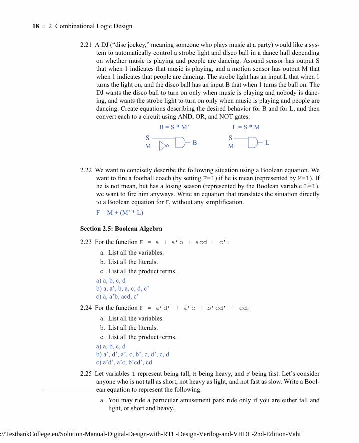
2.21 A DJ (“disc jockey,” meaning someone who plays music at a party) would like a sys-tem to automatically control a strobe light and disco ball in a dance hall dependingon whether music is playing and people are dancing. Asound sensor has output Sthat when 1 indicates that music is playing, and a motion sensor has output M thatwhen 1 indicates that people are dancing. The strobe light has an input L that when 1turns the light on, and the disco ball has an input B that when 1 turns the ball on. TheDJ wants the disco ball to turn on only when music is playing and nobody is danc-ing, and wants the strobe light to turn on only when music is playing and people aredancing. Create equations describing the desired behavior for B and for L, and thenconvert each to a circuit using AND, OR, and NOT gates.
B = S * M’ L = S * M
2.22 We want to concisely describe the following situation using a Boolean equation. Wewant to fire a football coach (by setting F=1) if he is mean (represented by M=1). Ifhe is not mean, but has a losing season (represented by the Boolean variable L=1),we want to fire him anyways. Write an equation that translates the situation directlyto a Boolean equation for F, without any simplification.F = M + (M’ * L)
Section 2.5: Boolean Algebra
2.23 For the function F = a + a’b + acd + c’:a. List all the variables.b. List all the literals.c. List all the product terms.
a) a, b, c, db) a, a’, b, a, c, d, c’c) a, a’b, acd, c’
2.24 For the function F = a’d’ + a’c + b’cd’ + cd:a. List all the variables.b. List all the literals.c. List all the product terms.
a) a, b, c, db) a’, d’, a’, c, b’, c, d’, c, dc) a’d’, a’c, b’cd’, cd
2.25 Let variables T represent being tall, H being heavy, and F being fast. Let’s consideranyone who is not tall as short, not heavy as light, and not fast as slow. Write a Bool-ean equation to represent the following:
a. You may ride a particular amusement park ride only if you are either tall andlight, or short and heavy.
SM B
SM L
Full file at http://TestbankCollege.eu/Solution-Manual-Digital-Design-with-RTL-Design-Verilog-and-VHDL-2nd-Edition-Vahi

2.1 Exercises b 19
b. You may NOT ride an amusement park ride if you are either tall and light, orshort and heavy. Use algebra to simplify the equation to sum of products.
c. You are eligible to play on a particular basketball team if you are tall and fast, ortall and slow. Simplify this equation.
d. You are NOT eligible to play on a particular football team if you are short andslow, or if you are light. Simplify to sum of products form.
e. You are eligible to play on both the basketball and football teams above, basedon the above criteria. Hint: combine the two equations into one equation byANDing them.
a) Ride = TH’ + T’Hb) Ride = (TH’ + T’H)’ = (TH’)’(T’H)’ = (T’ + H)(T + H’) = T’H’ + THc) Basketball = TF + TF’ = T(F+F’) = T(1) = Td) Football = (T’F’ + H’)’ = (T’F’)’H = (T + F)H = TH + FHe) BasketballAndFootball = T(TH + FH) = TTH + TFH = TH + TFH = TH(1+F) =TH. In other words, only people who are both tall and heavy can play on both teams.
2.26 Let variables S represent a package being small, H being heavy, and E being expen-sive. Let’s consider a package that is not small as big, not heavy as light, and notexpensive as inexpensive. Write a Boolean equation to represent the following:
a. Your company specializes in delivering packages that are both small and inex-pensive (a package must be small AND inexpensive for us to deliver it); you’llalso deliver packages that are big but only if they are expensive.
b. A particular truck can be loaded with packages only if the packages are smalland light, small and heavy, or big and light. Simplify the equation.
c. Your above-mentioned company buys the above-mentioned truck. Write anequation that describes the packages your company can deliver. Hint: Appropri-ately combine the equations from the above two parts.
a) Deliver = SE’ + S’Eb) Load = SH’ + SH + S’H’ = SH’ + SH + SH’ + S’H’ = S + H’c) Packages = Deliver*Load = (SE’ + S’E)*(S+H’) = SSE’ + SS’E + H’SE’ + H’S’E= SE’ + 0 + H’SE’ + H’S’E = (1+H’)SE’ + H’S’E = SE’ + S’EH’. In other words,you can deliver small inexpensive packages, or large expensive light packages.
2.27 Use algebraic manipulation to convert the following equation to sum-of-productsform: F = a(b + c)(d’) + ac’(b + d)F = (ab + ac)d’ + ac’b + ac’dF = abd’ + acd’ + ac’b + ac’d
2.28 Use algebraic manipulation to convert the following equation to sum-of-productsform: F = a’b(c + d’) + a(b’ + c) + a(b + d)cF = a’bc + a’bd’ + ab’ + ac + (ab + ad)cF = a’bc + a’bd’ + ab’ + ac + abc + acdF = a’bc + a’bd’ + ab’ + ac
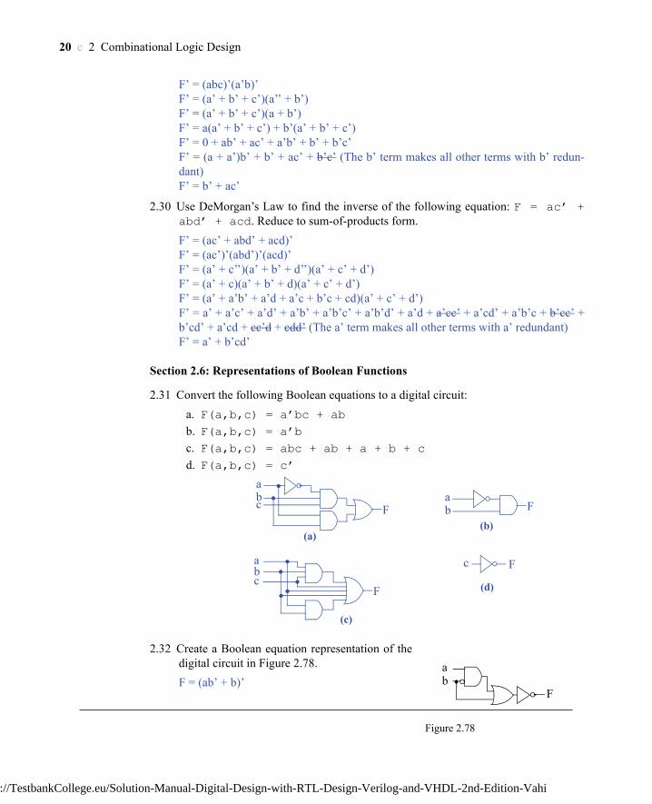
2.29 Use DeMorgan’s Law to find the inverse of the following equation: F = abc +a’b. Reduce to sum-of-products form. Hint: Start with F’ = (abc + a’b)’.F’ = (abc + a’b)’
Full file at http://TestbankCollege.eu/Solution-Manual-Digital-Design-with-RTL-Design-Verilog-and-VHDL-2nd-Edition-Vahi
20 c 2 Combinational Logic Design
F’ = (abc)’(a’b)’F’ = (a’ + b’ + c’)(a’’ + b’)F’ = (a’ + b’ + c’)(a + b’)F’ = a(a’ + b’ + c’) + b’(a’ + b’ + c’)F’ = 0 + ab’ + ac’ + a’b’ + b’ + b’c’F’ = (a + a’)b’ + b’ + ac’ + b’c’ (The b’ term makes all other terms with b’ redun-dant)F’ = b’ + ac’
2.30 Use DeMorgan’s Law to find the inverse of the following equation: F = ac’ +abd’ + acd. Reduce to sum-of-products form.F’ = (ac’ + abd’ + acd)’F’ = (ac’)’(abd’)’(acd)’F’ = (a’ + c’’)(a’ + b’ + d’’)(a’ + c’ + d’)F’ = (a’ + c)(a’ + b’ + d)(a’ + c’ + d’)F’ = (a’ + a’b’ + a’d + a’c + b’c + cd)(a’ + c’ + d’)F’ = a’ + a’c’ + a’d’ + a’b’ + a’b’c’ + a’b’d’ + a’d + a’cc’ + a’cd’ + a’b’c + b’cc’ +b’cd’ + a’cd + cc’d + cdd’ (The a’ term makes all other terms with a’ redundant)F’ = a’ + b’cd’
Section 2.6: Representations of Boolean Functions
2.31 Convert the following Boolean equations to a digital circuit:a. F(a,b,c) = a’bc + abb. F(a,b,c) = a’bc. F(a,b,c) = abc + ab + a + b + cd. F(a,b,c) = c’
2.32 Create a Boolean equation representation of thedigital circuit in Figure 2.78.F = (ab’ + b)’
(b)(a)
a
Fbc
F
(c)
aFb
abc
F
c
(d)
Figure 2.78
ab
F
Full file at http://TestbankCollege.eu/Solution-Manual-Digital-Design-with-RTL-Design-Verilog-and-VHDL-2nd-Edition-Vahi

2.1 Exercises b 21
2.33 Create a Boolean equation representation for thedigital circuit in Figure 2.79.F = (ab’ + b) + a’c
2.34 Convert each of the Boolean equations in Exer-cise 2.31 to a truth table.
2.35 Convert each of the following Boolean equations to a truth table:a. F(a,b,c) = a’ + bc’b. F(a,b,c) = (ab)’ + ac’ + bcc. F(a,b,c) = ab + ac + ab’c’ + c’d.F(a,b,c,d) = a’bc + d’
Figure 2.79
ab
Gc
Inputs Outputsa b c F0 0 0 00 0 1 00 1 0 00 1 1 11 0 0 01 0 1 01 1 0 11 1 1 1
Inputs Outputsa b c F0 0 0 00 0 1 00 1 0 10 1 1 11 0 0 01 0 1 01 1 0 01 1 1 0
Inputs Outputsa b c F0 0 0 00 0 1 10 1 0 10 1 1 11 0 0 11 0 1 11 1 0 11 1 1 1
Inputs Outputsa b c F0 0 0 10 0 1 00 1 0 10 1 1 01 0 0 11 0 1 01 1 0 11 1 1 0
(a) (b)
(c) (d)
Full file at http://TestbankCollege.eu/Solution-Manual-Digital-Design-with-RTL-Design-Verilog-and-VHDL-2nd-Edition-Vahi

22 c 2 Combinational Logic Design
2.36 Fill in Table 2.8’s columns for theequation: F= ab + b’
Inputs Outputsa b c F0 0 0 10 0 1 10 1 0 10 1 1 11 0 0 01 0 1 01 1 0 11 1 1 0
Inputs Outputsa b c F0 0 0 10 0 1 10 1 0 10 1 1 11 0 0 11 0 1 11 1 0 01 1 1 1
Inputs Outputsa b c F0 0 0 10 0 1 00 1 0 10 1 1 01 0 0 11 0 1 11 1 0 11 1 1 1
Inputs Outputsa b c d F0 0 0 0 10 0 0 1 00 0 1 0 10 0 1 1 00 1 0 0 10 1 0 1 00 1 1 0 10 1 1 1 11 0 0 0 11 0 0 1 01 0 1 0 11 0 1 1 01 1 0 0 11 1 0 1 01 1 1 0 11 1 1 1 0
(a) (b)
(c)
(d)
Table 2.8Inputs Outputa b ab b’ ab+b’ F0 0 0 1 1 10 1 0 0 0 01 0 0 1 1 11 1 1 0 1 1
Full file at http://TestbankCollege.eu/Solution-Manual-Digital-Design-with-RTL-Design-Verilog-and-VHDL-2nd-Edition-Vahi

2.1 Exercises b 23
2.37 Convert the function F shown in the truth table inTable 2.9 to an equation. Don’t minimize the equa-tion.F = a’b’c + a’bc’ + a’bc + ab’c + abc’ + abc
2.38 Use algebraic manipulation to minimize the equa-tion obtained in Exercise 2.37F = a’b’c + a’bc’ + a’bc + ab’c + abc’ + abcF = a’(b’c + bc’ + bc) + a(b’c + bc’ + bc)F = a’(b’c + b(c’ + c)) + a(b’c + b(c’ + c))F = a’(b’c + b) + a(b’c + b)F = (a’ + a)(b’c + b)F = b’c + b
2.39 Convert the function F shown in the truth table inTable 2.10 to an equation. Don’t minimize theequation.F = a’b’c’ + a’bc’ + ab’c’ + ab’c + abc’
2.40 Use algebraic manipulation to minimize the equa-tion obtained in Exercise 2.39F = a’b’c’ + a’bc’ + ab’c’ + ab’c + abc’F = a’(b’c’ + bc’) + a(b’c’ + b’c + bc’)F = a’((b’ + b)c’) + a(b’(c’ + c) + bc’)F = a’c’ + a(b’ + bc’)
2.41 Convert the function F shown in the truth table inTable 2.11 to an equation. Don’t minimize theequation.F = a’b’c + abc’ + abc
2.42 Use algebraic manipulation to minimize the equa-tion obtained in Exercise 2.41.F = a’b’c + abc’ + abcF = a’b’c + ab(c’ + c)F = a’b’c + ab
2.43 Create a truth table for the circuit of Figure 2.78
Table 2.9a b c F0 0 0 00 0 1 10 1 0 10 1 1 11 0 0 01 0 1 11 1 0 11 1 1 1
Table 2.10a b c F0 0 0 10 0 1 00 1 0 10 1 1 01 0 0 11 0 1 11 1 0 11 1 1 0
Table 2.11a b c F0 0 0 00 0 1 10 1 0 00 1 1 01 0 0 01 0 1 01 1 0 11 1 1 1
Full file at http://TestbankCollege.eu/Solution-Manual-Digital-Design-with-RTL-Design-Verilog-and-VHDL-2nd-Edition-Vahi

24 c 2 Combinational Logic Design
.
2.44 Create a truth table for the circuit of Figure 2.79.
2.45 Convert the function F shown in the truth table in Table 2.9 to a digital circuit.
2.46 Convert the function F shown in the truth table in Table 2.10 to a digital circuit.
2.47 Convert the function F shown in the truth table in Table 2.11 to a digital circuit.
2.48 Convert the following Boolean equations to canonical sum-of-minterms form:
Inputs Outputsa b F0 0 10 1 01 0 01 1 0
Inputs Outputsa b c ab’ + b a’c F0 0 0 0 0 00 0 1 0 1 10 1 0 1 0 10 1 1 1 1 11 0 0 1 0 11 0 1 1 0 11 1 0 1 0 11 1 1 1 0 1
F
bc
F
a
c
b
F
a
c
b
Full file at http://TestbankCollege.eu/Solution-Manual-Digital-Design-with-RTL-Design-Verilog-and-VHDL-2nd-Edition-Vahi
2.1 Exercises b 25
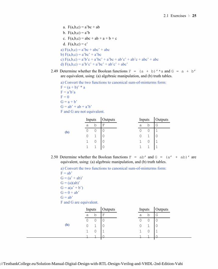
a. F(a,b,c) = a’bc + abb. F(a,b,c) = a’bc. F(a,b,c) = abc + ab + a + b + cd. F(a,b,c) = c’
a) F(a,b,c) = a’bc + abc’ + abcb) F(a,b,c) = a’bc’ + a’bcc) F(a,b,c) = a’b’c + a’bc’ + a’bc + ab’c’ + ab’c + abc’ + abcd) F(a,b,c) = a’b’c’ + a’bc’ + ab’c’ + abc’
2.49 Determine whether the Boolean functions F = (a + b)’*a and G = a + b’are equivalent, using: (a) algebraic manipulation, and (b) truth tables. a) Convert the two functions to canonical sum-of-minterms form:F = (a + b)’ * aF = a’b’aF = 0G = a + b’G = ab’ + ab + a’b’F and G are not equivalent.
2.50 Determine whether the Boolean functions F = ab’ and G = (a’ + ab)’ areequivalent, using: (a) algebraic manipulation, and (b) truth tables. a) Convert the two functions to canonical sum-of-minterms form:F = ab’G = (a’ + ab)’G = (a)(ab)’G = a(a’ + b’)G = 0 + ab’G = ab’F and G are equivalent.
Inputs Outputsa b F0 0 00 1 01 0 01 1 0
Inputs Outputsa b G0 0 10 1 01 0 11 1 1
(b)
Inputs Outputsa b F0 0 00 1 01 0 11 1 0
Inputs Outputsa b G0 0 00 1 01 0 11 1 0
(b)
Full file at http://TestbankCollege.eu/Solution-Manual-Digital-Design-with-RTL-Design-Verilog-and-VHDL-2nd-Edition-Vahi
26 c 2 Combinational Logic Design
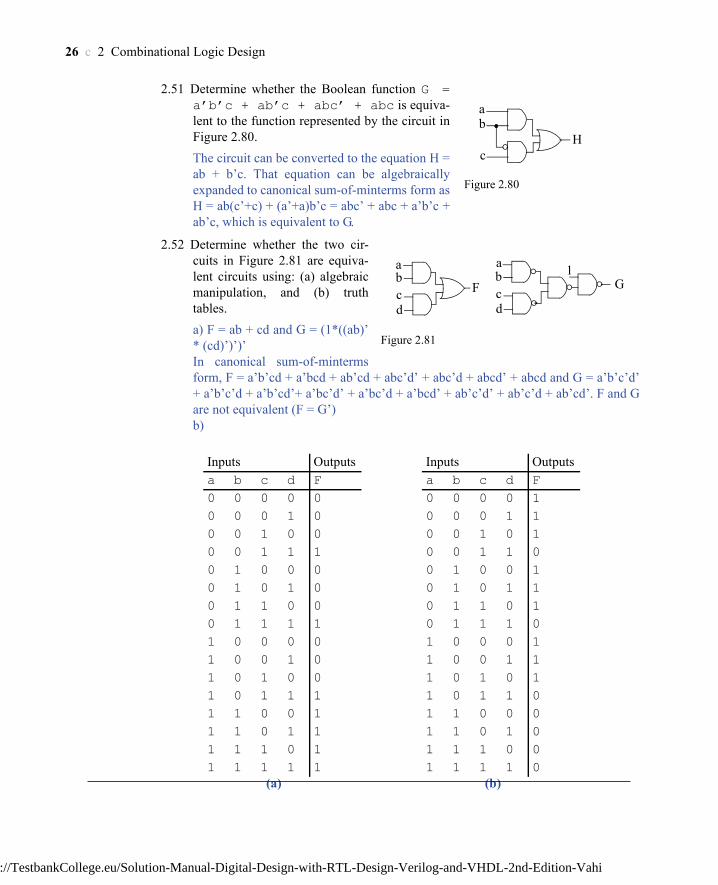
2.51 Determine whether the Boolean function G =a’b’c + ab’c + abc’ + abc is equiva-lent to the function represented by the circuit inFigure 2.80.The circuit can be converted to the equation H =ab + b’c. That equation can be algebraicallyexpanded to canonical sum-of-minterms form asH = ab(c’+c) + (a’+a)b’c = abc’ + abc + a’b’c +ab’c, which is equivalent to G.
2.52 Determine whether the two cir-cuits in Figure 2.81 are equiva-lent circuits using: (a) algebraicmanipulation, and (b) truthtables.a) F = ab + cd and G = (1*((ab)’* (cd)’)’)’In canonical sum-of-mintermsform, F = a’b’cd + a’bcd + ab’cd + abc’d’ + abc’d + abcd’ + abcd and G = a’b’c’d’+ a’b’c’d + a’b’cd’+ a’bc’d’ + a’bc’d + a’bcd’ + ab’c’d’ + ab’c’d + ab’cd’. F and Gare not equivalent (F = G’)b)
Figure 2.80
ab
Hc
Figure 2.81
ab
Fcd
b Gcd
a 1
Inputs Outputsa b c d F0 0 0 0 00 0 0 1 00 0 1 0 00 0 1 1 10 1 0 0 00 1 0 1 00 1 1 0 00 1 1 1 11 0 0 0 01 0 0 1 01 0 1 0 01 0 1 1 11 1 0 0 11 1 0 1 11 1 1 0 11 1 1 1 1
(a)
Inputs Outputsa b c d F0 0 0 0 10 0 0 1 10 0 1 0 10 0 1 1 00 1 0 0 10 1 0 1 10 1 1 0 10 1 1 1 01 0 0 0 11 0 0 1 11 0 1 0 11 0 1 1 01 1 0 0 01 1 0 1 01 1 1 0 01 1 1 1 0
(b)
Full file at http://TestbankCollege.eu/Solution-Manual-Digital-Design-with-RTL-Design-Verilog-and-VHDL-2nd-Edition-Vahi
2.1 Exercises b 27
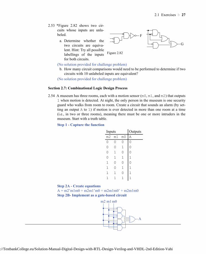
2.53 *Figure 2.82 shows two cir-cuits whose inputs are unla-beled.
a. Determine whether thetwo circuits are equiva-lent. Hint: Try all possiblelabellings of the inputsfor both circuits.
(No solution provided for challenge problem)b. How many circuit comparisons would need to be performed to determine if two
circuits with 10 unlabeled inputs are equivalent?(No solution provided for challenge problem)
Section 2.7: Combinational Logic Design Process
2.54 A museum has three rooms, each with a motion sensor (m0, m1, and m2) that outputs1 when motion is detected. At night, the only person in the museum is one securityguard who walks from room to room. Create a circuit that sounds an alarm (by set-ting an output A to 1) if motion is ever detected in more than one room at a time(i.e., in two or three rooms), meaning there must be one or more intruders in themuseum. Start with a truth table.Step 1 - Capture the function
Step 2A - Create equationsA = m2’m1m0 + m2m1’m0 + m2m1m0’ + m2m1m0Step 2B- Implement as a gate-based circuit
Figure 2.82
G
F
Inputs Outputsm2 m1 m0 A0 0 0 00 0 1 00 1 0 00 1 1 11 0 0 01 0 1 11 1 0 11 1 1 1
m1 m0m2
A
Full file at http://TestbankCollege.eu/Solution-Manual-Digital-Design-with-RTL-Design-Verilog-and-VHDL-2nd-Edition-Vahi

28 c 2 Combinational Logic Design
2.55 Create a circuit for the museum of Exercise 2.54 that detects whether the guard isproperly patrolling the museum, detected by exactly one motion sensor being 1. (Ifno motion sensor is 1, the guard may be sitting, sleeping, or absent). Step 1 - Capture the function
Step 2A - Create equationsA = m2’m1’m0 + m2’m1m0’ + m2m1’m0’Step 2B- Implement as a gate-based circuit
Inputs Outputsm2 m1 m0 A0 0 0 00 0 1 10 1 0 10 1 1 01 0 0 11 0 1 01 1 0 01 1 1 0
m1 m0m2
A
Full file at http://TestbankCollege.eu/Solution-Manual-Digital-Design-with-RTL-Design-Verilog-and-VHDL-2nd-Edition-Vahi

2.1 Exercises b 29
2.56 Consider the museum security alarm function of Exercise 2.54, but for a museumwith 10 rooms. A truth table is not a good starting point (too many rows), nor is anequation describing when the alarm should sound (too many terms). However, theinverse of the alarm function can be straightforwardly captured as an equation.Design the circuit for the 10 room security system, by designing the inverse of thefunction, and then just adding an inverter before the circuit’s output. Step 1 - Capture the functionThe inverse function detects that motion is detected by exactly one motion sensor, orno motion sensor detecting motion; all the other possibilities are for two or moresensors detecting motion. Thus, the inverse function can be written as:A’ =m9m8’m7’m6’m5’m4’m3’m2’m1’m0’ + m9’m8m7’m6’m5’m4’m3’m2’m1’m0’ +m9’m8’m7m6’m5’m4’m3’m2’m1’m0’ + m9’m8’m7’m6m5’m4’m3’m2’m1’m0’ +m9’m8’m7’m6’m5m4’m3’m2’m1’m0’ + m9’m8’m7’m6’m5’m4m3’m2’m1’m0’ +m9’m8’m7’m6’m5’m4’m3m2’m1’m0’ + m9’m8’m7’m6’m5’m4’m3’m2m1’m0’ +m9’m8’m7’m6’m5’m4’m3’m2’m1m0’ + m9’m8’m7’m6’m5’m4’m3’m2’m1’m0 +m9’m8’m7’m6’m5’m4’m3’m2’m1’m0’The first term is for motion sensor m9 detecting motion and all others detecting nomotion, the second term is for m8, and so on. That last term is for no sensor detect-ing motion. Step 2A - Create equationsAlready done. Step 2B- Implement as a gate-based circuit
m9m8m7m6m5m4m3m2m1m0
A
Full file at http://TestbankCollege.eu/Solution-Manual-Digital-Design-with-RTL-Design-Verilog-and-VHDL-2nd-Edition-Vahi

30 c 2 Combinational Logic Design
2.57 A network router connects multiple computers together and allows them to sendmessages to each other. If two or more computers send messages simultaneously,the messages “collide” and the messages must be resent. Using the combinationaldesign process of Table 2.5, create a collision detection circuit for a router that con-nects 4 computers. The circuit has 4 inputs labeled M0 through M3 that are 1 whenthe corresponding computer is sending a message and 0 otherwise. The circuit hasone output labeled C that is 1 when a collision is detected and 0 otherwise.Step 1 - Capture the function A truth table is convenient for this problem.
Step 2A - Create equationWe note that there are more 1s in the output column than there are 0s. Thus, wechoose to create an equation for the inverse of the function, and we’ll then add aninverter at the output. The problem could also be solved by creating a (longer) equa-tion for the function itself rather than the inverse. C’ = M3’M2’M1’M0’ + M3’M2’M1’M0 + M3’M2’M1M0’ + M3’M2M1’M0’ +M3M2’M1’M0’
Inputs OutputsM3 M2 M1 M0 C0 0 0 0 00 0 0 1 00 0 1 0 00 0 1 1 10 1 0 0 00 1 0 1 10 1 1 0 10 1 1 1 11 0 0 0 01 0 0 1 11 0 1 0 11 0 1 1 11 1 0 0 11 1 0 1 11 1 1 0 11 1 1 1 1
Full file at http://TestbankCollege.eu/Solution-Manual-Digital-Design-with-RTL-Design-Verilog-and-VHDL-2nd-Edition-Vahi

2.1 Exercises b 31
Step 2B- Implement as a gate-based circuit
2.58 Using the combinational design process of Table 2.5, create a 4-bit prime numberdetector. The circuit has four inputs, N3, N2, N1, and N0 that correspond to a 4-bitnumber (N3 is the most significant bit) and one output P that is 1 when the input is aprime number and that is 0 otherwise.Step 1 - Capture the functionThe prime numbers in the range 0-15 are 2, 3, 5, 7, 11, and 13. Rows whose inputbinary number correspond to those numbers have P set to a 1; the other rows get 0.
Step 2A - Create equationsP = N3’N2’N1N0’ + N3’N2’N1N0 + N3’N2N1’N0 + N3’N2N1N0 + N3N2’N1N0+ N3N2N1’N0
M3M2M1M0
C
Inputs OutputsN3 N2 N1 N0 P0 0 0 0 00 0 0 1 00 0 1 0 10 0 1 1 10 1 0 0 00 1 0 1 10 1 1 0 00 1 1 1 11 0 0 0 01 0 0 1 01 0 1 0 01 0 1 1 11 1 0 0 01 1 0 1 11 1 1 0 01 1 1 1 0
Full file at http://TestbankCollege.eu/Solution-Manual-Digital-Design-with-RTL-Design-Verilog-and-VHDL-2nd-Edition-Vahi

32 c 2 Combinational Logic Design
Step 2B - Implement as a gate-based circuit
2.59 A car has a fuel-level detector that outputs the current fuel-level as a 3-bit binarynumber, with 000 meaning empty and 111 meaning full. Create a circuit that illu-minates a “low fuel” indicator light (by setting an output L to 1) when the fuel leveldrops below level 3. Step 1 - Capture the function
Step 2A -Create equationsL = F2’F1’F0’ + F2’F1’F0 + F2’F1F0’Step 2B- Implement as a gate-based circuit
2.60 A car has a low-tire-pressure sensor that outputs the current tire pressure as a 5-bitbinary number. Create a circuit that illuminates a “low tire pressure” indicator light(by setting an output T to 1) when the tire pressure drops below 16. Hint: you mightfind it easier to create a circuit that detects the inverse function. You can then justappend an inverter to the output of that circuit. Step 1 - Capture the function
N3N2N1N0
P
Inputs OutputsF2 F1 F0 L0 0 0 10 0 1 10 1 0 10 1 1 01 0 0 01 0 1 01 1 0 01 1 1 0
F2F1F0
L
Full file at http://TestbankCollege.eu/Solution-Manual-Digital-Design-with-RTL-Design-Verilog-and-VHDL-2nd-Edition-Vahi

2.1 Exercises b 33
The inverse function outputs 1 if the input is 16 or greater. For a 5-bit number, weknow that any number 16 or greater has a 1 in the leftmost bit, which we’ll name P4.Any number less than 16 will have a 0 in P4. Thus, an equation that detects 16 orgreater is just: T’ = P4Step 2A - Create equationsAlready done3 - Implement as a gate-based circuit
Section 2.8: More Gates
2.61 Show the conduction paths and output value of the NAND gate transistor circuit inFigure 2.54 when: (a) x = 1 and y = 0, (b) x = 1 and y = 1.
2.62 Show the conduction paths and output value of the NOR gate transistor circuit inFigure 2.54 when: (a) x = 1 and y = 0, (b) x = 0 and y = 0.
2.63 Show the conduction paths and output value of the AND gate transistor circuit inFigure 2.55 when: (a) x = 1 and y = 1, (b) x = 0 and y = 1.
P4 T
xF
1
0y
y
x
xF
1
0y
y
x
(a) (b)
1 0
(a) (b)
0xF
1
0
y
y
x
1xF
1
0
y
y
x
(a) (b)
01F
1
0
x1
0y
y
x F
1
0
x1
0y
y
x
Full file at http://TestbankCollege.eu/Solution-Manual-Digital-Design-with-RTL-Design-Verilog-and-VHDL-2nd-Edition-Vahi

34 c 2 Combinational Logic Design
2.64 Two people, denoted using variables A and B, want to ride with you on your motor-cycle. Write a Boolean equation that indicates that exactly one of the two people cancome (A=1 means A can come, A=0 means A can’t come). Then use XOR to sim-plify your equation.F = A’B + AB’F = A XOR B
2.65 Simplify the following equation by using XOR wherever possible: F = a’b +ab’ + cd’ + c’d + ac.F = (a XOR b) + (c XOR d) + ac
2.66 Use 2-input XOR gates to create a circuit that outputs a 1 when the number of 1s oninputs a, b, c, d is odd.
2.67 Use 2-input XOR or XNOR gates to create a circuit that detects if an even number ofthe inputs a, b, c, d are 1s.
Section 2.9: Decoders and Muxes
2.68 Design a 3x8 decoder using AND, OR and NOT gates.
2.69 Design a 4x16 decoder using AND, OR and NOT gates.
F
abcd
F
abcd
i2i1i0
d7 d6 d5 d4 d3 d2 d1 d0
i2i1i0
d9 d8 d7 d6 d5 d4 d3 d2 d1 d0d15 d14 d13 d12 d11 d10
i3
Full file at http://TestbankCollege.eu/Solution-Manual-Digital-Design-with-RTL-Design-Verilog-and-VHDL-2nd-Edition-Vahi
2.1 Exercises b 35
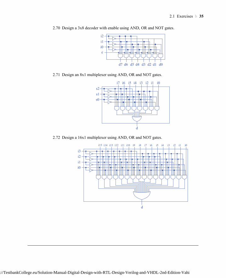
2.70 Design a 3x8 decoder with enable using AND, OR and NOT gates.
2.71 Design an 8x1 multiplexer using AND, OR and NOT gates.
2.72 Design a 16x1 multiplexer using AND, OR and NOT gates.
i2i1i0
d7 d6 d5 d4 d3 d2 d1 d0
e
s2s1s0
d
i7 i6 i5 i4 i3 i2 i1 i0
i2i1i0
i9 i8 i7 i6 i5 i4 i3 i2 i1 i0i15 i14 i13 i12 i11 i10
i3
d
Full file at http://TestbankCollege.eu/Solution-Manual-Digital-Design-with-RTL-Design-Verilog-and-VHDL-2nd-Edition-Vahi

36 c 2 Combinational Logic Design
2.73 Design a 4-bit 4x1 multiplexer using four 4x1 multiplexors.
2.74 A house has four external doors each with a sensor that outputs 1 if its door is open.Inside the house is a single LED that a homeowner wishes to use to indicate whethera door is open or closed. Because the LED can only show the status of one sensor,the homeowner buys a switch that can be set to 0, 1, 2, or 3 and that has a 2-bit out-put representing the switch position in binary. Create a circuit to connect the foursensors, the switch, and the LED. Use at least one mux (a single mux or an N-bitmux) or decoder. Use block symbols with a clearly defined function, such as “2x1mux,” “8-bit 2x1 mux,” or “3x8 decoder”; do not show the internal design of a muxor decoder..
i3 i2 i1 i0
s1s0
d
s1s0
d
s1s0
d
s1s0
d
s1s0
i3[3]i2[3]
i1[3]i0[3]
i3 i2 i1 i0
i3[2]i2[2]
i1[2]i0[2]
i3 i2 i1 i0
i3[1]i2[1]
i1[1]i0[1]
i3 i2 i1 i0
i3[0]i2[0]
i1[0]i0[0]
d3 d2 d1 d0
LED
d3 d2
i3 i2
ds1
4x1 MuxSwitch
s0
d1 d0
i1 i0
(0, 1, 2, or 3
Full file at http://TestbankCollege.eu/Solution-Manual-Digital-Design-with-RTL-Design-Verilog-and-VHDL-2nd-Edition-Vahi

2.1 Exercises b 37
2.75 A video system can accept video from one of two video sources, but can only displayone source at a given time. Each source outputs a stream of digitized video on itsown 8-bit output. A switch with a single bit output chooses which of the two 8-bitstreams will be passed on a display’s single 8-bit input. Create a circuit to connectthe two video sources, the switch, and the display. Use at least one mux (a singlemux or an N-bit mux) or decoder. Use block symbols with a clearly defined func-tion, such as “2x1 mux,” “8-bit 2x1 mux,” or “3x8 decoder”; do not show the inter-nal design of a mux or decoder.
2.76 A store owner wishes to be able to indicate to customers that the items in one of thestore’s eight aisles are temporarily discounted (“on sale”). The store owner thusmounts a light above each aisle, and each light has a single bit input that turns on thelight when 1. The store owner has a switch that can be set to 0, 1, 2, 3, 4, 5, 6, or 7,and that has a 3-bit output representing the switch position in binary. A secondswitch can be set up or down and has a single bit output that is 1 when the switch isup; the store owner can set this switch down if no aisles are currently discounted.Use at least one mux (a single mux or an N-bit mux) or decoder. Use block symbolseach with a clearly defined function, such as “2x1 mux,” “8-bit 2x1 mux,” or “3x8decoder”; do not show the internal design of a mux or decoder.
to display
Source B Source A
i1 i0
d
8-bit2x1 Muxs0Switch
8
8 8
e
i2Switch (0 to 7)
Switch (up ordown)
i1i0
d7d6d5d4d3d2d1d0
3x8 decoder(with enable)
to aisle7
to aisle0
Full file at http://TestbankCollege.eu/Solution-Manual-Digital-Design-with-RTL-Design-Verilog-and-VHDL-2nd-Edition-Vahi

38 c 2 Combinational Logic Design
Section 2.10: Additional Considerations
2.77 Determine the critical path of the specified circuit. Assume that each AND and ORgate has a delay of 1 ns, each NOT gate has a delay of 0.75 ns, and each wire has adelay of 0.5 ns.
a. The circuit of Figure 2.37.The path from input c to output F has a delay of 0.5 + 0.75 + 0.5 + 1 + 0.5 = 3.25 ns.The path from input h to output F has a delay of 0.5 + 1 + 0.5 + 1 + 0.5 = 3.5 nsThe path from input p to output F has a delay of 0.5 + 1 + 0.5 + 1 + 0.5 = 3.5 ns.The longest path is 3.5 ns. Thus, the circuit’s critical path is 3.5 ns.
b. The circuit of Figure 2.41.The path from input a to output F has a delay of 0.5 + 1 + 0.5 + 0.75 + 0.5 + 1 + 0.5= 4.75 ns. The path from input b to output F is identical to that from input a: 4.75 ns. The path from input c to output F has a delay of 0.5 + 0.75 + 0.5 + 1 + 0.5 = 3.25 ns.The longest path is 4.75 ns. Thus, the circuit’s critical path is 4.75 ns.
2.78 Design a 1x4 demultiplexer using AND, OR and NOT gates.
s1s0
d3
i
d2 d1 d0
Full file at http://TestbankCollege.eu/Solution-Manual-Digital-Design-with-RTL-Design-Verilog-and-VHDL-2nd-Edition-Vahi
2.1 Exercises b 39
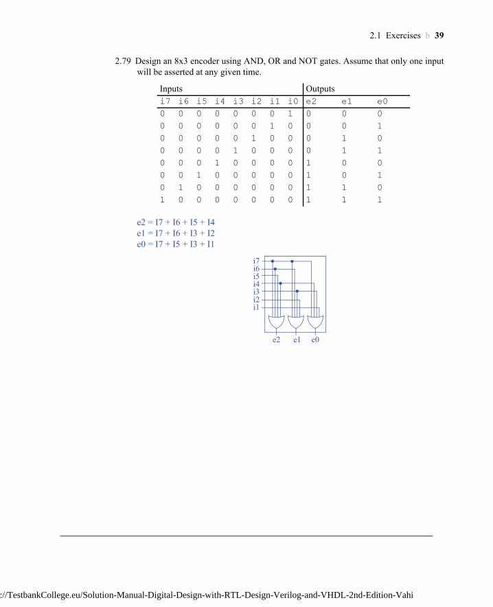
2.79 Design an 8x3 encoder using AND, OR and NOT gates. Assume that only one inputwill be asserted at any given time.
e2 = I7 + I6 + I5 + I4e1 = I7 + I6 + I3 + I2e0 = I7 + I5 + I3 + I1
Inputs Outputsi7 i6 i5 i4 i3 i2 i1 i0 e2 e1 e00 0 0 0 0 0 0 1 0 0 00 0 0 0 0 0 1 0 0 0 10 0 0 0 0 1 0 0 0 1 00 0 0 0 1 0 0 0 0 1 10 0 0 1 0 0 0 0 1 0 00 0 1 0 0 0 0 0 1 0 10 1 0 0 0 0 0 0 1 1 01 0 0 0 0 0 0 0 1 1 1
i7i6i5i4i3i2i1
e2 e1 e0
Full file at http://TestbankCollege.eu/Solution-Manual-Digital-Design-with-RTL-Design-Verilog-and-VHDL-2nd-Edition-Vahi

40 c 2 Combinational Logic Design
2.80 Design a 4x2 priority encoder using AND, OR and NOT gates. If every input is 0,the output should be “00”.
e1 = i3 + i2e0 = i3 + i2’i1
Inputs Outputsi3 i2 i1 i0 e1 e00 0 0 0 0 00 0 0 1 0 00 0 1 0 0 10 0 1 1 0 10 1 0 0 1 00 1 0 1 1 00 1 1 0 1 00 1 1 1 1 01 0 0 0 1 11 0 0 1 1 11 0 1 0 1 11 0 1 1 1 11 1 0 0 1 11 1 0 1 1 11 1 1 0 1 11 1 1 1 1 1
i3i2
i1
e1
e0
Full file at http://TestbankCollege.eu/Solution-Manual-Digital-Design-with-RTL-Design-Verilog-and-VHDL-2nd-Edition-Vahi