COHERENT/INCOHERENT MAGNETIZATION DYNAMICS OF …
112
Virginia Commonwealth University VCU Scholars Compass eses and Dissertations Graduate School 2017 COHERENT/INCOHERENT MAGNETIZATION DYNAMICS OF NANOMAGNETIC DEVICES FOR ULT- LOW ENERGY COMPUTING Md Mamun Al-Rashid Virginia Commonwealth University Follow this and additional works at: hps://scholarscompass.vcu.edu/etd Part of the Nanotechnology Fabrication Commons , and the Other Electrical and Computer Engineering Commons © Md Mamun Al-Rashid is Dissertation is brought to you for free and open access by the Graduate School at VCU Scholars Compass. It has been accepted for inclusion in eses and Dissertations by an authorized administrator of VCU Scholars Compass. For more information, please contact [email protected]. Downloaded from hps://scholarscompass.vcu.edu/etd/5109
Transcript of COHERENT/INCOHERENT MAGNETIZATION DYNAMICS OF …

Virginia Commonwealth UniversityVCU Scholars Compass
Theses and Dissertations Graduate School
2017
COHERENT/INCOHERENTMAGNETIZATION DYNAMICS OFNANOMAGNETIC DEVICES FOR ULTRA-LOW ENERGY COMPUTINGMd Mamun Al-RashidVirginia Commonwealth University
Follow this and additional works at: https://scholarscompass.vcu.edu/etd
Part of the Nanotechnology Fabrication Commons, and the Other Electrical and ComputerEngineering Commons
© Md Mamun Al-Rashid
This Dissertation is brought to you for free and open access by the Graduate School at VCU Scholars Compass. It has been accepted for inclusion inTheses and Dissertations by an authorized administrator of VCU Scholars Compass. For more information, please contact [email protected].
Downloaded fromhttps://scholarscompass.vcu.edu/etd/5109
COHERENT/INCOHERENT MAGNETIZATION DYNAMICS OF NANOMAGNETIC
DEVICES FOR ULTRA-LOW ENERGY COMPUTING
A dissertation submitted in partial fulfillment of the requirements for the degree of Doctor of
Philosophy at Virginia Commonwealth University.
By
Md Mamun Al-Rashid
Bachelor of Science in Electrical and Electronic Engineering, Bangladesh University of
Engineering and Technology, 2012
Director: Jayasimha Atulasimha,
Professor, Department of Mechanical and Nuclear Engineering, and Electrical and
Computer Engineering.
Virginia Commonwealth University
Richmond, Virginia
October, 2017
ii
Acknowledgement
I would like to acknowledge the tremendous guidance and support provided my Ph.D. supervisor
Professor Jayasimha Atulasimha throughout the course of my graduate studies and research. He
has been a source of great motivation for me and has helped me overcome many challenges and
obstacles both in my academic and personal life. I am also very grateful to Professor Supriyo
Bandyopadhyay, whose mentorship and suggestions have been instrumental in the successful
completion of this thesis.
I would like to acknowledge the contributions of the members of my dissertation committee –
Professor Umit Ozgur, Professor Shiv Khanna, Professor Ravi Hadimani and Professor Dafiné
Ravelosona. Their invaluable suggestions and feedbacks have positively impacted my journey as
a researcher and substantially improved this dissertation.
I would like to thank our research collaborators – Prof. Greg Carman, Prof. Amit Trivedi, Dr.
Brian Kirby, Dr. Guillaume Agnus and Dr. Thomas Maroutian, all of whom have invaluable
contributions in many of the works presented in this thesis.
I am grateful to my peers and colleagues Dr. Mohammad Salehi Fashami, Dr. Noel D’Souza, Dr.
Vimal Sampath, Dr. Ayan Biswas, Dr. Hasnain Ahmed, Dr. Iftekhar Hossain, Dr. Barkat Ullah,
Dhritiman Bhattacharya, Romit Ghosh, Kallol Roy, Md Ali Azam and many more including the
great staffs in the VCU School of Engineering, who have made this journey pleasant and
remarkable.
I am thankful for the academic and financial support provided by VCU School of Engineering,
VCU Graduate School, National Science Foundation for the NSF CAREER grant CCF 1253370
iii
and Nanoelectronics Beyond 2020 ECCS-1124714, Virginia CIT and VCU Quest
Commercialization Grant.
Finally, and most importantly, I would like to thank my parents Md Noor Islam and Most Arjuma
Begum, my younger brother Md Mehedi Hasan, my wife Al Hera Islam and other family members
for their continued love, support, and motivation. None of this would have been possible without
them.
iv
Table of Contents
List of Figures……………………………………………………………………………………vi
List of Tables…………………………………………………………………………………….xi
Abstract…………………………………………………………………………………………xii
Chapter 1: Introduction…………………………………………………………………………1
1.1. Nanomagnetic Devices……………………………………………………………………2
1.2. Magnetostriction and Villari Effect……………………………………………………….5
1.3. Single Domain Approximation Modeling of Magnetization Dynamics…………………..5
1.4. Dipole Coupled Nanomagnetic Computing……………………………………………...10
1.5. Micromagnetic Modeling of Magnetization Dynamics………………………………….11
1.6. Polarized Neutron Reflectometry………………………………………………………..14
1.7. Dissertation Outline……………………………………………………………………...16
Chapter 2: Geometry Effect on Performance of Strain Switched Dipole Coupled
Nanomagnetic Logic……………………………………………………………………………18
2.1. Simulation Conditions: Stress Application………………………………………………….21
2.2. Switching Time Estimate……………………………………………………………………22
2.3. Comparison between the Elliptical and Cylindrical Geometries In Terms Of Switching Time
or Switching Speed………………………………………………………………………………23
2.4. Switching Error Estimate……………………………………………………………………24
v
2.5. Comparison between the Elliptical and Cylindrical Geometries in terms of Switching
Error……………………………………………………………………………………………...25
2.6. Conclusion…………………………………………………………………………………..28
Chapter 3: Strain Clocked Scalable Nanomagnetic Logic Wire…………………………….30
3.1. Information Propagation in an Array of Circular Nanomagnets with Thermal Noise……...32
3.2. Experimental Demonstration………………………………………………………………..37
3.3. Conclusion…………………………………………………………………………………..40
Chapter 4: Dynamic Error in Strain-Induced Magnetization Reversal of Nanomagnets Due
to Incoherent Switching and Formation of Metastable States: A Size-Dependent Study….41
4.1. Size Dependence of the Switching Coherency……………………………………………...43
4.2. Switching Coherency Dependence of Dynamic Error………………………………………45
4.3. Energy Dissipation Estimates……………………………………………………………….49
4.4. Conclusion…………………………………………………………………………………..50
Chapter 5: Skewed Straintronic MTJ (ss-MTJ) for Ternary Content Addressable
Memory………………………………………………………………………………………….52
5.1. Skewed Straintronic Magneto Tunneling Junction………………………………………….53
5.2. TCAM Implementation…………………………………………………………………...…61
5.3. Comparison between ss-MTJ and CMOS based TCAM……………………………………62
5.4. Conclusion…………………………………………………………………………………..63
vi
Chapter 6: Polarized Neutron Reflectometry Study of Depth Dependent Magnetization
Variation in Co Thin Films…………………………………………………………………….64
6.1. Experimental Preparation……………………………………………………………………64
6.2. Investigation of Strain Effect on Coercive Field and Coherent vs. Incoherent Switching….65
6.3. Depth Dependent Magnetization Rotation…………………………………………………..69
6.4. Repeatability………………………………………………………………………………...75
6.5. Conclusion…………………………………………………………………………………..76
Chapter 7: Summary and Future Directions……………………………………………..…..78
7.1. Summary…………………………………………………………………………………….78
7.2. Future Directions……………………………………………………………………………79
7.2.1. Foundations for low voltage switching……………………………………………………80
7.2.2. Scaling to 50 nm & beyond and improved switching error……………………………….82
References…………………………………………………………………………...…………..83
Author Biography and List of Publications………………………………………...………...95
vii
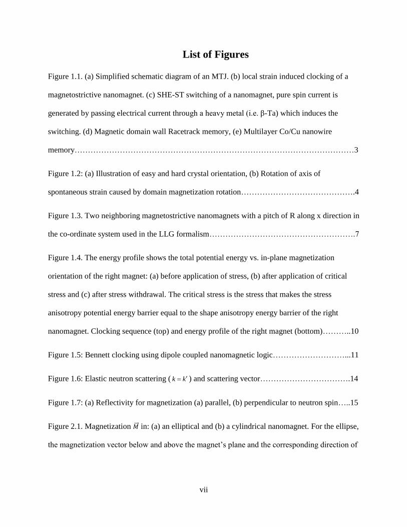
List of Figures
Figure 1.1. (a) Simplified schematic diagram of an MTJ. (b) local strain induced clocking of a
magnetostrictive nanomagnet. (c) SHE-ST switching of a nanomagnet, pure spin current is
generated by passing electrical current through a heavy metal (i.e. β-Ta) which induces the
switching. (d) Magnetic domain wall Racetrack memory, (e) Multilayer Co/Cu nanowire
memory……………………………………………………………………………………………3
Figure 1.2: (a) Illustration of easy and hard crystal orientation, (b) Rotation of axis of
spontaneous strain caused by domain magnetization rotation…………………………………….4
Figure 1.3. Two neighboring magnetostrictive nanomagnets with a pitch of R along x direction in
the co-ordinate system used in the LLG formalism……………………………………………….7
Figure 1.4. The energy profile shows the total potential energy vs. in-plane magnetization
orientation of the right magnet: (a) before application of stress, (b) after application of critical
stress and (c) after stress withdrawal. The critical stress is the stress that makes the stress
anisotropy potential energy barrier equal to the shape anisotropy energy barrier of the right
nanomagnet. Clocking sequence (top) and energy profile of the right magnet (bottom)………..10
Figure 1.5: Bennett clocking using dipole coupled nanomagnetic logic………………………...11
Figure 1.6: Elastic neutron scattering ( k k ) and scattering vector…………………………….14
Figure 1.7: (a) Reflectivity for magnetization (a) parallel, (b) perpendicular to neutron spin…..15
Figure 2.1. Magnetization �⃗⃗� in: (a) an elliptical and (b) a cylindrical nanomagnet. For the ellipse,
the magnetization vector below and above the magnet’s plane and the corresponding direction of
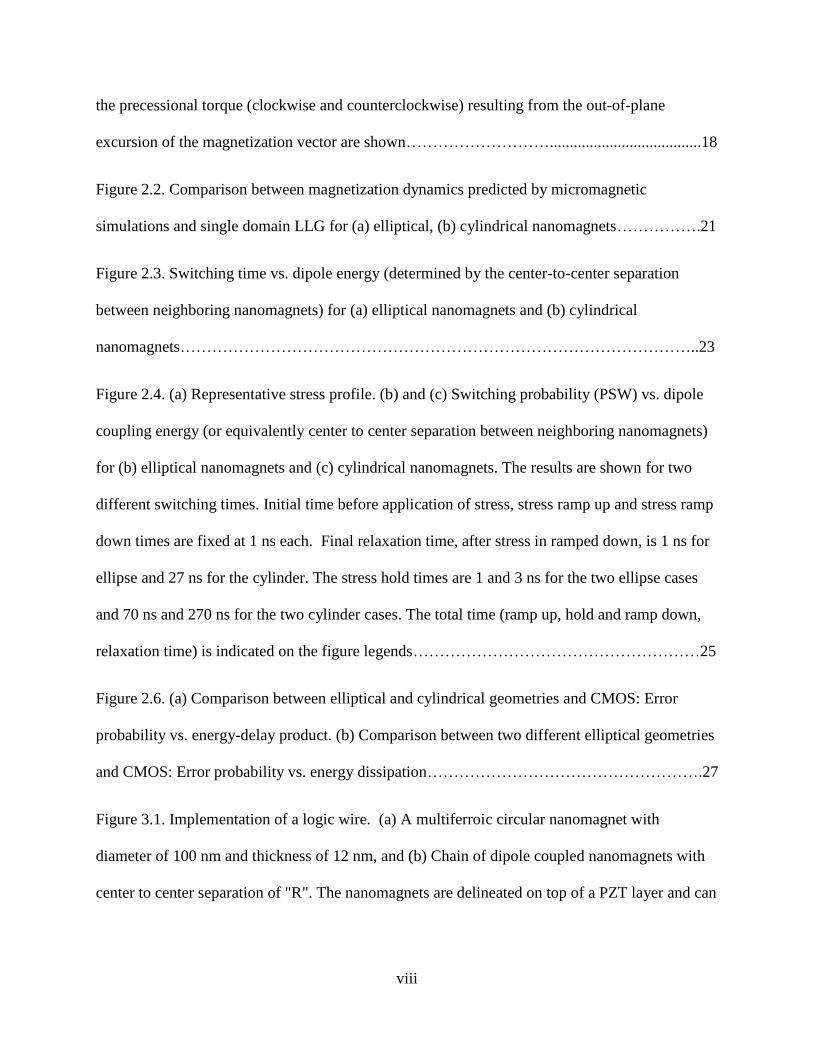
viii
the precessional torque (clockwise and counterclockwise) resulting from the out-of-plane
excursion of the magnetization vector are shown………………………......................................18
Figure 2.2. Comparison between magnetization dynamics predicted by micromagnetic
simulations and single domain LLG for (a) elliptical, (b) cylindrical nanomagnets…………….21
Figure 2.3. Switching time vs. dipole energy (determined by the center-to-center separation
between neighboring nanomagnets) for (a) elliptical nanomagnets and (b) cylindrical
nanomagnets……………………………………………………………………………………..23
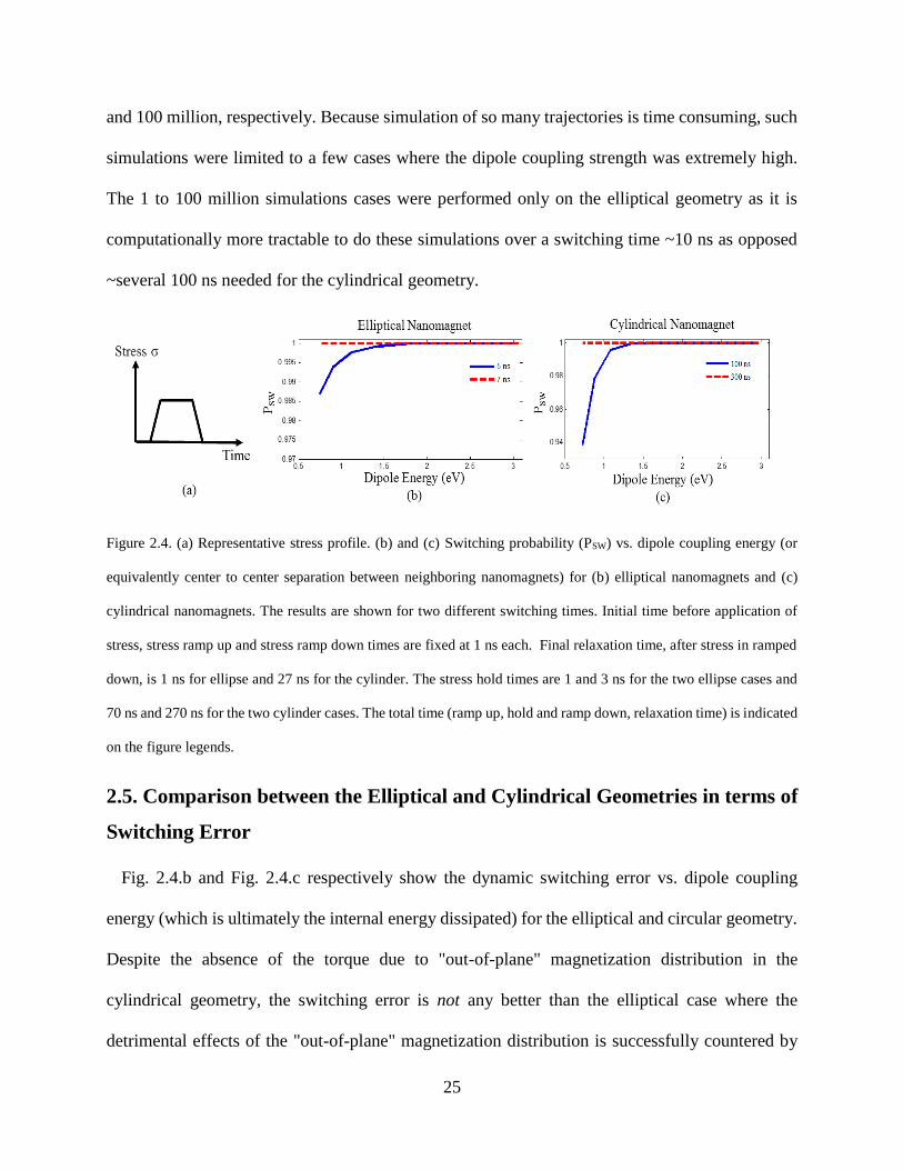
Figure 2.4. (a) Representative stress profile. (b) and (c) Switching probability (PSW) vs. dipole
coupling energy (or equivalently center to center separation between neighboring nanomagnets)
for (b) elliptical nanomagnets and (c) cylindrical nanomagnets. The results are shown for two
different switching times. Initial time before application of stress, stress ramp up and stress ramp
down times are fixed at 1 ns each. Final relaxation time, after stress in ramped down, is 1 ns for
ellipse and 27 ns for the cylinder. The stress hold times are 1 and 3 ns for the two ellipse cases
and 70 ns and 270 ns for the two cylinder cases. The total time (ramp up, hold and ramp down,
relaxation time) is indicated on the figure legends………………………………………………25
Figure 2.6. (a) Comparison between elliptical and cylindrical geometries and CMOS: Error
probability vs. energy-delay product. (b) Comparison between two different elliptical geometries
and CMOS: Error probability vs. energy dissipation…………………………………………….27
Figure 3.1. Implementation of a logic wire. (a) A multiferroic circular nanomagnet with
diameter of 100 nm and thickness of 12 nm, and (b) Chain of dipole coupled nanomagnets with
center to center separation of "R". The nanomagnets are delineated on top of a PZT layer and can
ix
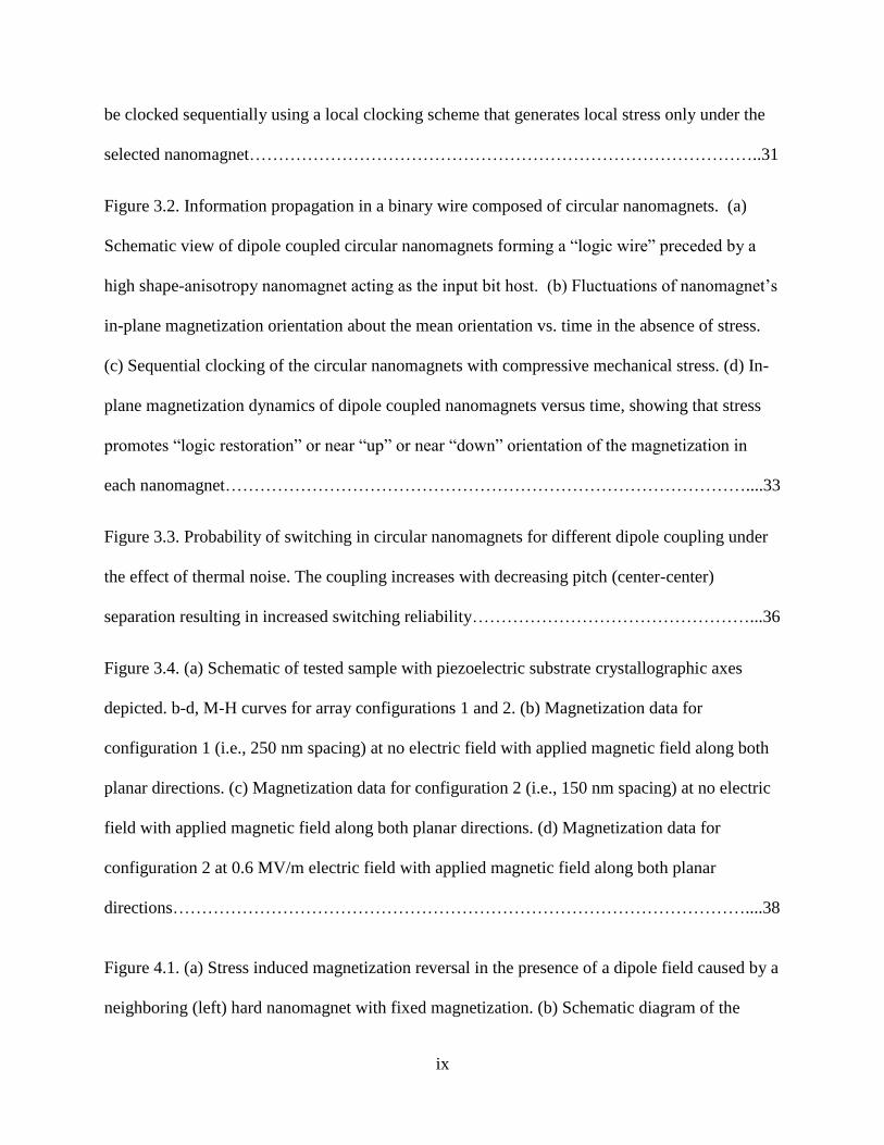
be clocked sequentially using a local clocking scheme that generates local stress only under the
selected nanomagnet……………………………………………………………………………..31
Figure 3.2. Information propagation in a binary wire composed of circular nanomagnets. (a)
Schematic view of dipole coupled circular nanomagnets forming a “logic wire” preceded by a
high shape-anisotropy nanomagnet acting as the input bit host. (b) Fluctuations of nanomagnet’s
in-plane magnetization orientation about the mean orientation vs. time in the absence of stress.
(c) Sequential clocking of the circular nanomagnets with compressive mechanical stress. (d) In-
plane magnetization dynamics of dipole coupled nanomagnets versus time, showing that stress
promotes “logic restoration” or near “up” or near “down” orientation of the magnetization in
each nanomagnet………………………………………………………………………………....33
Figure 3.3. Probability of switching in circular nanomagnets for different dipole coupling under
the effect of thermal noise. The coupling increases with decreasing pitch (center-center)
separation resulting in increased switching reliability…………………………………………...36
Figure 3.4. (a) Schematic of tested sample with piezoelectric substrate crystallographic axes
depicted. b-d, M-H curves for array configurations 1 and 2. (b) Magnetization data for
configuration 1 (i.e., 250 nm spacing) at no electric field with applied magnetic field along both
planar directions. (c) Magnetization data for configuration 2 (i.e., 150 nm spacing) at no electric
field with applied magnetic field along both planar directions. (d) Magnetization data for
configuration 2 at 0.6 MV/m electric field with applied magnetic field along both planar
directions………………………………………………………………………………………....38
Figure 4.1. (a) Stress induced magnetization reversal in the presence of a dipole field caused by a
neighboring (left) hard nanomagnet with fixed magnetization. (b) Schematic diagram of the
x
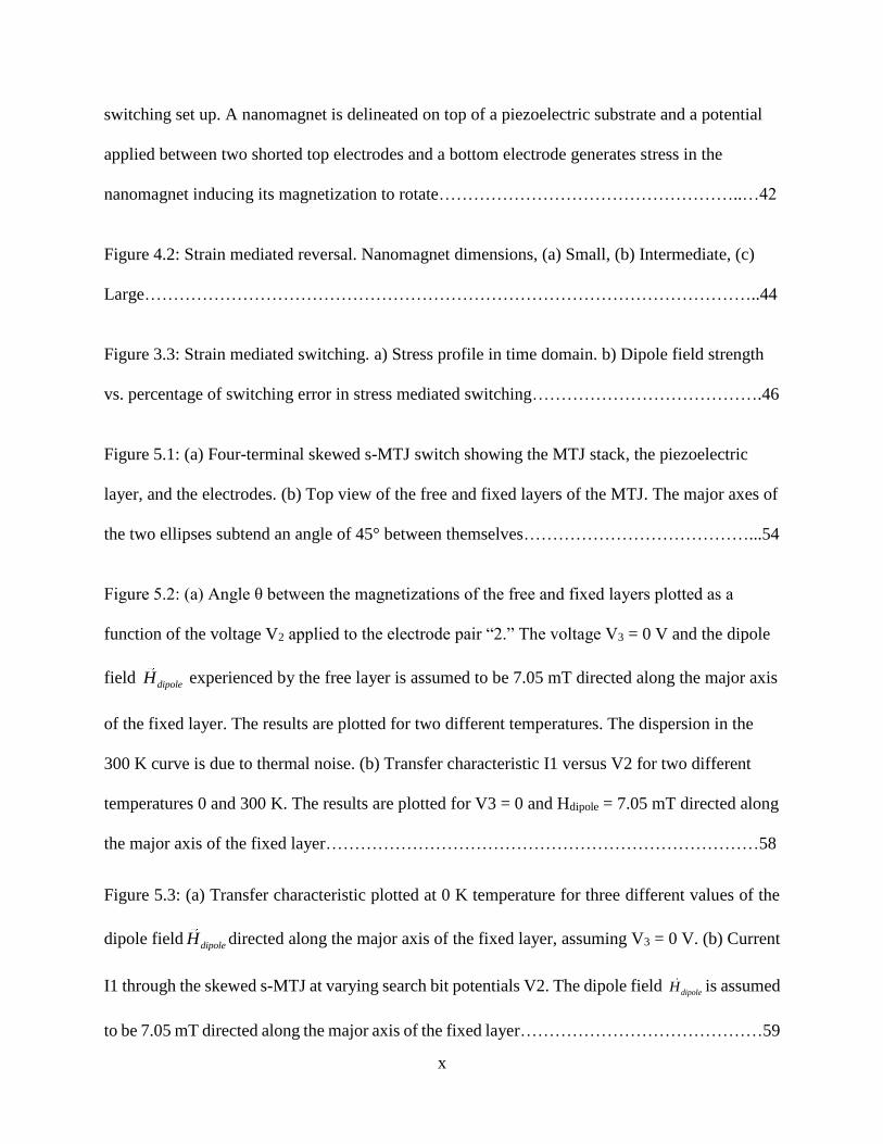
switching set up. A nanomagnet is delineated on top of a piezoelectric substrate and a potential
applied between two shorted top electrodes and a bottom electrode generates stress in the
nanomagnet inducing its magnetization to rotate……………………………………………..…42
Figure 4.2: Strain mediated reversal. Nanomagnet dimensions, (a) Small, (b) Intermediate, (c)
Large……………………………………………………………………………………………..44
Figure 3.3: Strain mediated switching. a) Stress profile in time domain. b) Dipole field strength
vs. percentage of switching error in stress mediated switching………………………………….46
Figure 5.1: (a) Four-terminal skewed s-MTJ switch showing the MTJ stack, the piezoelectric
layer, and the electrodes. (b) Top view of the free and fixed layers of the MTJ. The major axes of
the two ellipses subtend an angle of 45° between themselves…………………………………...54
Figure 5.2: (a) Angle θ between the magnetizations of the free and fixed layers plotted as a
function of the voltage V2 applied to the electrode pair “2.” The voltage V3 = 0 V and the dipole
field dipoleH experienced by the free layer is assumed to be 7.05 mT directed along the major axis
of the fixed layer. The results are plotted for two different temperatures. The dispersion in the
300 K curve is due to thermal noise. (b) Transfer characteristic I1 versus V2 for two different
temperatures 0 and 300 K. The results are plotted for V3 = 0 and Hdipole = 7.05 mT directed along
the major axis of the fixed layer…………………………………………………………………58
Figure 5.3: (a) Transfer characteristic plotted at 0 K temperature for three different values of the
dipole field dipoleH directed along the major axis of the fixed layer, assuming V3 = 0 V. (b) Current
I1 through the skewed s-MTJ at varying search bit potentials V2. The dipole field dipoleH is assumed
to be 7.05 mT directed along the major axis of the fixed layer……………………………………59
xi
Figure 5.4: ss-MTJ-based dynamic TCAM cell…………………………………………………..61
Figure 6.1: (a) Sample schematic, (b) Typical reflectivity measurement using PNR……………..65
Figure 6.2: Reflectivity vs. applied magnetic field at 10.16 Q nm coming up from negative
saturation for applied voltages of (a) 0V, (b) 150V, (c) 300V, (d) 400V……………………….66
Figure 6.3: (a) Spin asymmetry vs. magnetic field and (b) spin flip scattering vs. magnetic field
at different applied voltages……………………………………………………………………...67
Figure 6.4: Magnetization reversal scenarios for different anisotropy magnitude………………68
Figure 6.5: Reflectivity data and model fitting for 700 mT, 0V………………………………....69
Figure 6.6: Reflectivity data and corresponding fit at remanence (1 mT) for (a) 0V and (b)
400V……………………………………………………………………………………………...71
Figure 6.7: Reflectivity data and corresponding fit at coercive field (10 mT) for (a) 0V and (b)
400V……………………………………………………………………………………………...73
Figure 7.1: Local strain induced clocking of magnetostrictive nanomagnets. The nanomagnets
can be clocked individually by applying an electric potential across the corresponding
terminals…………………………………………………………………………………….........80
Figure 7.2: (a) Fabrication of large electrodes for external connection. (b) Fabrication of
electrodes with lateral dimension equal to the PZT film thickness. (c) Fabrication of the
magnetostrictive nanomagnets…………………………………………………………………...81
Figure 7.3: Height and Magnetic phase image obtained via MFM……………………………...81
xii
List of Tables
Table 1.1: Write energy and write speed in various nanomagnetic memory devices…………......4
Table 4.1: Simulated nanomagnet dimensions…………………………………………………..41
Table 4.2: Material properties of Terfenol-D…………………………………………………....43
Table 4.3. Energy dissipation in stress mediated switching……………………………………..49
Table 5.1: Voltage levels used to encode store and search bits………………………………….60
Table 6.1: Fitted model parameters in saturation………………………………………………...70
Table 6.2: Fitted model parameters at remanence……………………………………………….72
Table 6.3: Fitted model parameters at coercive field…………………………………………….74
Table 6.4: Fitted model parameters at remanence……………………………………………….75
xiii
Abstract
Title of Dissertation: COHERENT/INCOHERENT MAGNETIZATION DYNAMICS OF
NANOMAGNETIC DEVICES FOR ULTRA-LOW ENERGY COMPUTING.
By Md Mamun Al-Rashid
A dissertation submitted in partial fulfillment of the requirements for the degree of Doctor of
Philosophy at Virginia Commonwealth University.
Virginia Commonwealth University, 2017.
Major Director: Jayasimha Atulasimha, Professor, Department of Mechanical and Nuclear
Engineering, and Electrical and Computer Engineering.
Nanomagnetic computing devices are inherently nonvolatile and show unique transfer
characteristics while their switching energy requirements are on par, if not better than state of the
art CMOS based devices. These characteristics make them very attractive for both Boolean and
non-Boolean computing applications. Among different strategies employed to switch
nanomagnetic computing devices e.g. magnetic field, spin transfer torque, spin orbit torque etc.,
strain induced switching has been shown to be among the most energy efficient. Strain switched
nanomagnetic devices are also amenable for non-Boolean computing applications. Such strain
mediated magnetization switching, termed here as “Straintronics”, is implemented by switching
the magnetization of the magnetic layer of a magnetostrictive-piezoelectric nanoscale
heterostructure by applying an electric field in the underlying piezoelectric layer. The modes of
“straintronic” switching: coherent vs. incoherent switching of spins can affect device performance
such as speed, energy dissipation and switching error in such devices. There was relatively little
research performed on understanding the switching mechanism (coherent vs. incoherent) in
xiv
straintronic devices and their adaptation for non-Boolean computing, both of which have been
studied in this thesis. Detailed studies of the effects of nanomagnet geometry and size on the
coherence of the switching process and ultimately device performance of such strain switched
nanomagnetic devices have been performed. These studies also contributed in optimizing designs
for low energy, low dynamic error operation of straintronic logic devices and identified avenues
for further research. A Novel non-Boolean “straintronic” computing device (Ternary Content
Addressable Memory, abbreviated as TCAM) has been proposed and evaluated through numerical
simulations. This device showed significant improvement over existing CMOS device based
TCAM implementation in terms of scaling, energy-delay product, operational simplicity etc. The
experimental part of this thesis answered a very fundamental question in strain induced
magnetization rotation. Specifically, this experiment studied the variation in magnetization
orientation for strain induced magnetization rotation along the thickness of a magnetostrictive thin
film using polarized neutron reflectometry and demonstrated non-uniform magnetization rotation
along the thickness of the sample. Additional experimental work was performed to lay the
groundwork for ultra-low voltage straintronic switching demonstration. Preliminary sample
fabrication and characterization that can potentially lead to low voltage (~10-100 mV) operation
and local clocking of such devices has been performed.
1
Chapter 1: Introduction
Nanomagnetic devices, where binary information is encoded in stable magnetization orientations
to perform memory and/or logic operations [1], [2] are promising alternatives to conventional
CMOS based computing. Owing to the exchange interaction, electron spins in a nanomagnet tends
to behave collectively which significantly lowers the theoretical limit of internal energy dissipation
to “switch” the devices compared to charge based ones [3]. Apart from the potential to be
extremely energy efficient, these devices are inherently non-volatile and can be used for both logic
and memory applications leading to novel computational architectures [4], [5] with improved
performance and energy efficiency. However, the energy dissipation required for switching
critically depends on the external mechanism employed for reversing the magnetization orientation
and an inefficient clocking mechanism can nullify the advantage of nanomagnetic devices. Among
the different switching paradigms, strain induced switching is among the most energy-efficient
techniques [6]–[9]. This work studies extensively, both theoretically and experimentally, the
straintronic switching of magnetization and their applications in Boolean and non-Boolean
computing. Detailed numerical simulations and state of the art experimental techniques have been
utilized to study the magnetization dynamics at room temperature and its effects on device
performance, to design and simulate novel devices, and to identify future research directions. This
chapter introduces various nanomagnetic devices, the basic principles behind straintronic devices,
macrospin and micromagnetic modeling of magnetization dynamics, examples of nanomagnetic
computing and a special magnetic characterization technique- polarized neutron reflectometry
(PNR) which can resolve magnetization variation along the thickness of a sample.
2
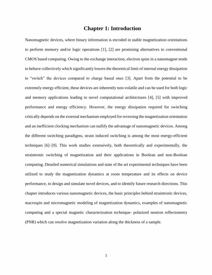
1.1. Nanomagnetic Devices
The most common type of structure used to implement logic and memory operations using
nanomagnets is the Magnetic Tunnel Junction (MTJ). A typical MTJ structure consists of a tunnel
barrier (typically metallic oxides i.e. MgO) sandwiched between a magnetically fixed layer and a
free layer as shown in Figure 1.1.a. A number of techniques to switch (or rotate) the magnetization
of the free layer have been explored, such as, external magnetic field induced switching [10], spin
transfer torque (STT) induced switching implemented by passing an electrical current through a
magnetic multilayer [11], [12], stress induced switching of a magnetostrictive nanomagnet brought
about by applying an electric potential to an underlying piezoelectric substrate [6], [7], [13], [14]
(Figure 1.1.b) and spin torque mediated switching due to pure spin current generated by the giant
spin Hall effect (SHE) in a heavy metal [15], [16] (Figure 1.1.c). Among these strategies, stress
induced switching is possibly the most energy efficient. Simulations have shown that a stress
clocked dipole coupled nanomagnetic NOT logic gate can be switched in ~1ns with energy
dissipation as low as 0.6 aJ and dynamic error probability less than 10-8 [9]. However, in practice
this is hard to attain due to lithographic variations and small magnetoelastic coupling which leads
to low effective magnetic field due to strain. Estimates based on experimentally demonstrated
stress-induced switching of ~200-300 nm lateral dimension elliptical Co and FeGa nanomagnets
delineated on a piezoelectric PMN-PT substrate predict that the energy dissipated in the switching
process could be as low as a few aJ if the nanomagnets are fabricated on a ~100 nm thin
piezoelectric film [7], [17]. However, in all experimental demonstrations to date, voltages applied
are typically in the kilovolts range as bulk piezoelectric substrates are used instead of thin films.
3
Figure 1.1. (a) Simplified schematic diagram of an MTJ. (b) local strain induced clocking of a magnetostrictive
nanomagnet [18]. (c) SHE-ST switching of a nanomagnet, pure spin current is generated by passing electrical current
through a heavy metal (i.e. β-Ta) which induces the switching [15]. (d) Magnetic domain wall Racetrack memory,
image sourced from Parkin et al. Science 320.5873 (2008): 190-194. (e) Multilayer Co/Cu nanowire memory.
Other structures include racetrack like memories [19] (Figure 1.1.d) and multilayered nanowires
with multiple Ferromagnetic (FM)/Nonmagnetic (NM) bilayers [20], [21] (Figure 1.1.e).[20], [21].
These structures are very promising for high density memory applications. In racetrack memory,
data is encoded in the domain magnetization of multi-domain magnetic nanowires [19]. Data is
read by measuring tunnel magnetoresistance using MTJ like structures connected to the nanowire
and written by fringing fields from domain walls (DW) in another perpendicular to the racetrack.
Individual bits are accessed by moving the DWs using current pulses. Multilayered nanowire
structures consists of multiple FM/NM bilayers i.e. Co/Cu. The FM layers typically have stable
parallel (P) and anti-parallel (AP) orientation which encodes the binary data. The layers can be
switched from P to AP or AP to P orientations using spin transfer torques and the resulting change
4
in giant magnetoresistance can be detected by passing a lower “sense” current in the read cycle.
Multilayer nanowire structures can be fabricated using cheap electrodeposition techniques and
have the potential to encode multiple bits in a single nanowire, further increasing the memory
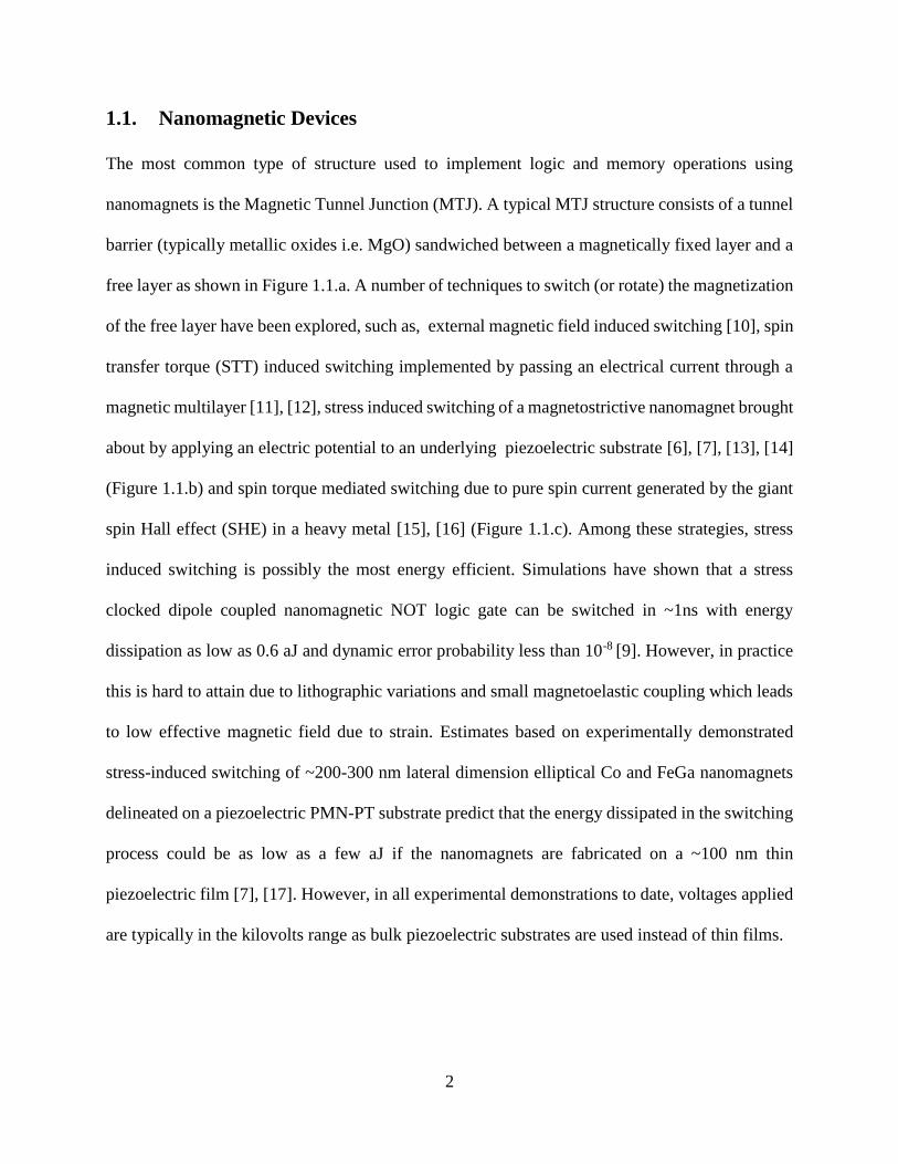
density. Table 1.1 shows the write energy consumption and write speed of different nanomagnet
based memory devices.
Table 1.1: Write energy and write speed in various nanomagnetic memory devices [15], [22]–
[28].
Nanomagnetic Device Write Energy Write Time (ns)
Spin Transfer Torque ~100 fJ 1-10
Giant Spin Hall Effect/ Spin Orbit Torque <1 fJ 1-10
Domain Wall/ Racetrack <1 fJ ~10
Magnetoelectric RAM based on Voltage Controlled
Magnetic Anisotropy and precessional switching
< 10 fJ 1-10
Straintronic Memory (estimated) ~10 aJ 1-10
Figure 1.2: (a) Illustration of easy and hard crystal orientation, (b) Rotation of axis of spontaneous strain caused by
domain magnetization rotation, image taken from [29].
5
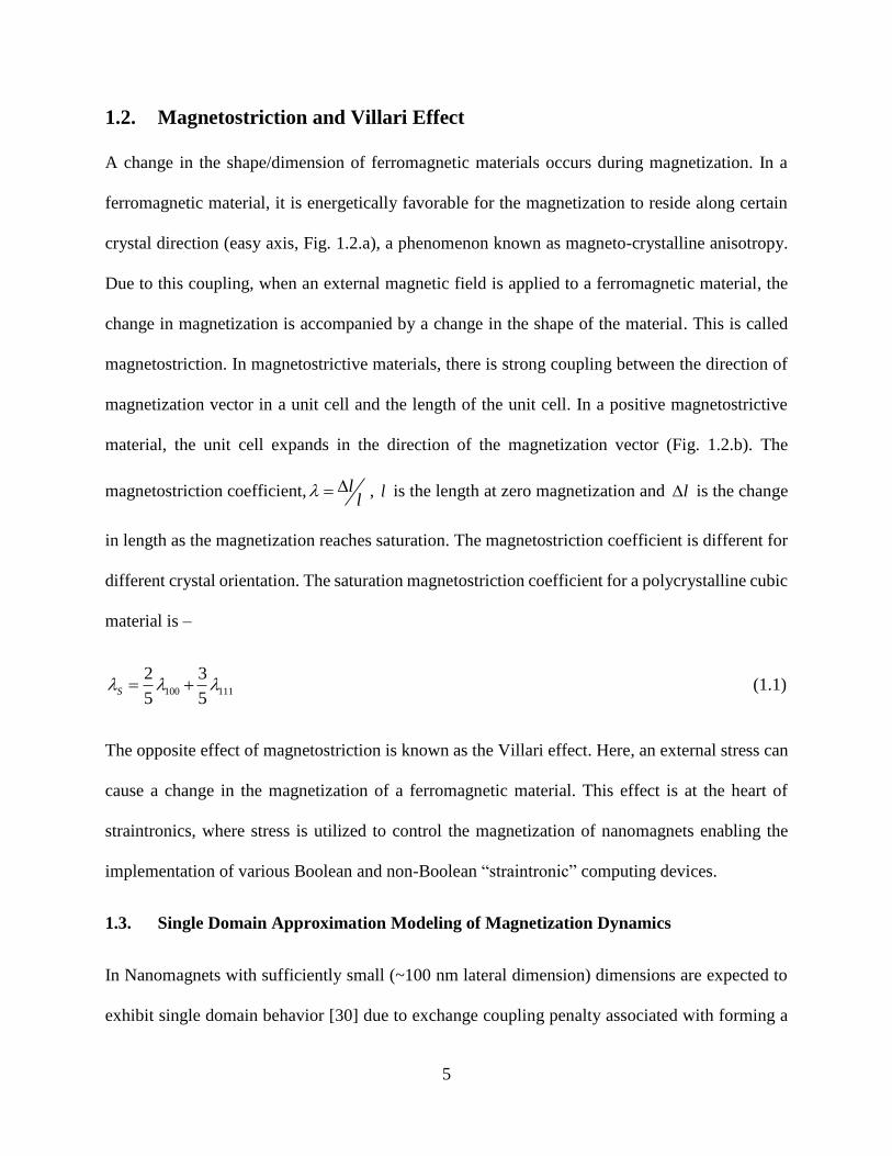
1.2. Magnetostriction and Villari Effect
A change in the shape/dimension of ferromagnetic materials occurs during magnetization. In a
ferromagnetic material, it is energetically favorable for the magnetization to reside along certain
crystal direction (easy axis, Fig. 1.2.a), a phenomenon known as magneto-crystalline anisotropy.
Due to this coupling, when an external magnetic field is applied to a ferromagnetic material, the
change in magnetization is accompanied by a change in the shape of the material. This is called
magnetostriction. In magnetostrictive materials, there is strong coupling between the direction of
magnetization vector in a unit cell and the length of the unit cell. In a positive magnetostrictive
material, the unit cell expands in the direction of the magnetization vector (Fig. 1.2.b). The
magnetostriction coefficient, ll
, l is the length at zero magnetization and l is the change
in length as the magnetization reaches saturation. The magnetostriction coefficient is different for
different crystal orientation. The saturation magnetostriction coefficient for a polycrystalline cubic
material is –
100 111
2 3
5 5S (1.1)
The opposite effect of magnetostriction is known as the Villari effect. Here, an external stress can
cause a change in the magnetization of a ferromagnetic material. This effect is at the heart of
straintronics, where stress is utilized to control the magnetization of nanomagnets enabling the
implementation of various Boolean and non-Boolean “straintronic” computing devices.
1.3. Single Domain Approximation Modeling of Magnetization Dynamics
In Nanomagnets with sufficiently small (~100 nm lateral dimension) dimensions are expected to
exhibit single domain behavior [30] due to exchange coupling penalty associated with forming a
6
multi-domain state. All the spins in these nanomagnets act as a giant single spin and rotate in
unison. The spatial variation in magnetization in the nanomagnets can therefore be ignored. The
behavior and magnetization dynamics of a nanomagnet under single domain approximation can
be modeled using the Landau-Lifshitz-Gilbert equation [31]–[33] –
eff eff
S
dM tM t H t M t M t H t
dt M
(1.2)
where effH t is the effective magnetic field. In strain switched shape anisotropic
magnetostrictive nanomagnet effH t includes effective fields due to stress, shape-anisotropy and
dipole coupling with neighbor(s). It is given by the derivative of the total potential energy E t
with respect to the magnetization ( )M t :
0
1
Ωeff
E tH t
M t
, (1.3)
where 𝑀𝑆 is the saturation magnetization of the nanomagnet, 𝜇0 is the permeability of vaccum, 𝛾
is the gyromagnetic ratio, Ω is the volume of the nanomagnet, and 𝛼 is the Gilbert damping
constant. The first term on the right hand side of equation (1.2) relates to the precessional torque
and the second term to the damped-mode torque.
The total energy E(t) in (1.3) is [8], [34]:
dipole stress anisotropy shape anisotropyE t E t E t E t (1.4)
where dipoleE t is the dipole coupling energy due to interaction between the two nanomagnets,
shape anisotropyE t is the shape anisotropy energy due to the elliptical or cylindrical shape of the
7
nanomagnet, and stress anisotropyE t is the stress anisotropy energy due to the stress generated in the
nanomagnet.
The effect of thermal noise is incorporated by adding an equivalent field thermalH t to the total
effective field:
0
1
Ωeff thermal
E tH t H t
M t
(1.5)
It is modeled as a random field [35].
0
2
ΩΔthermal
S
kTH t G t
M t
(1.6)
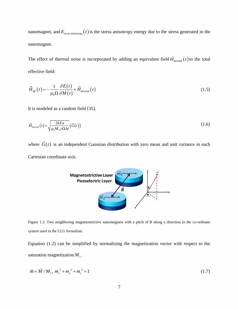
where G t is an independent Gaussian distribution with zero mean and unit variance in each
Cartesian coordinate axis.
Figure 1.3. Two neighboring magnetostrictive nanomagnets with a pitch of R along x direction in the co-ordinate
system used in the LLG formalism.
Equation (1.2) can be simplified by normalizing the magnetization vector with respect to the
saturation magnetization sM .
2 2 2/ , 1s x y zm M M m m m (1.7)
8
where xm , ym and zm are the x, y and z component of the normalized magnetization vector m
respectively that are given by:
sin cos , sin sin , cosx y zm t t t m t t t m t t (1.8)
Using these relations, the vector LLG equation can be decomposed into two coupled scalar
equations that describe the time evolution of the azimuthal () and polar () angles of the
magnetization vector:
2
2
( ) 1[cos ( ){ ( ( ) ( ) ( ) ( )) ( ( ) ( ) ( )
cos ( )
( ) ( ) ( ) ( ) ( ))} sin ( ){ ( ( ) ( ) ( ) ( ))
( ( ) ( ) ( )
eff z y eff y z eff y x y eff x y
eff x z eff z x z eff x z eff z x
eff z y z eff
d tt H t m t H t m t H m t m t H m t
dt t
H t m t H t m t m t t H t m t H t m t
H t m t m t H
2 2( ) ( ) ( ) ( ) ( ) ( ) ( ))}]y z eff y x eff x x yt m t H t m t H t m t m t
(1.9)
2
2
( ) 1[sin ( ){ ( ( ) ( ) ( ) ( )) ( ( ) ( ) ( )
sin ( )
( ) ( ) ( ) ( ) ( ))} cos ( ){ ( ( ) ( ) ( ) ( ))
( ( ) ( ) ( )
eff z y eff y z eff y x y eff x y
eff x z eff z x z eff x z eff z x
eff z y z eff
d tt H t m t H t m t H m t m t H m t
dt t
H t m t H t m t m t t H t m t H t m t
H t m t m t H
2 2( ) ( ) ( ) ( ) ( ) ( ) ( ))}]y z eff y x eff x x yt m t H t m t H t m t m t
(1.10)
Here, eff xH
, eff yH
and eff zH are the x, y and z components of the effective magnetic field effH
that are evaluated using (1.5) and (1.6).
Assuming the magnetizations of the two nanomagnets shown in Figure 1.3 have polar and
azimuthal angles of 1 t , 1 t and 2 t , 2 t respectively, the dipole interaction and shape
contributions to the potential energy of the second nanomagnet can be expressed as:
2 2
01 1 2 23
1 1 2 2 1 2
Ω [ 2
4
]
Sdipole
ME t sin t cos t sin t cos t
R
sin t sin t sin t sin t cos t cos t
(1.11)
9
22
0 2 2
2 2
2 2 2
Ω[
2
]
Sshape anisotropy d xx
d yy d zz
ME t N sin t cos t
N sin t sin t N cos t
(1.12)
Here d xxN ,d yyN
and d zzN are the demagnetization factors along the x, y and z directions and
satisfy the condition
1d xx d yy d zzN N N . (1.13)
The two type of shapes considered in this work are elliptical and circular cylinders. The
demagnetization factors of these shapes can be calculated using the formalism described in
Beleggia et al. [36].
In all cases in this work, stress is considered uniaxial. The corresponding stress anisotropy energy
for uniaxial stress along ith direction:
2
(3 / 2) Ωstress anisotropy s iE t m (1.14)
where (3 / 2) s is the saturation magnetostriction and is the applied uniaxial stress. We can
calculate the energies for the second nanomagnet in a similar manner. The resulting expressions
for the effective fields of a dipole coupled nanomagnet (where ˆR Rx ) for a uniaxial stress applied
along y direction are:
3
0
Ω 22sin cos sin cos
4 ΩΔ
i seff x j j s d xx i i x
S
M kTH t t t M N t t G t
R M t
3
0
0
Ω 3sin sin sin si( n ) sin sin
4
2
ΩΔ
i s seff y j j s d xx i i i i i
s
y
S
MH t t t M N t t t t
R M
kTG t
M t
(1.15)
10
3
0
Ω 2cos cos
4 ΩΔ
i seff z j s d xx i z
S
M kTH t t M N t G t
R M t
1.4. Dipole Coupled Nanomagnetic Computing
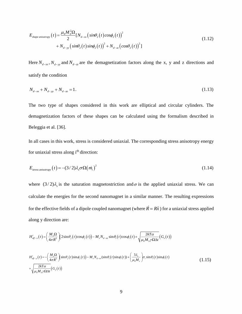
Figure 1.4 shows the total potential energy and corresponding magnetization direction of strain-
clocking of a dipole coupled pair of ellipsoidal nanomagnets to implement a Boolean NOT gate.
The left nanomagnet’s magnetization encodes the input bit and the right nanomagnet’s
magnetization encodes the output bit. The right nanomagnet is stressed locally to make its
magnetization rotate. Upon withdrawal of the stress, the right nanomagnet’s magnetization
preferentially assumes an orientation anti-parallel to that of the left’s because of dipole coupling
with the left neighbor, thereby realizing the Boolean NOT operation (output is the logic
complement of the input). The red ball in the energy profiles depicts the in-plane magnetization
orientation of the magnetization vector of the right magnet during the clocking sequence.
Figure 1.4. The energy profile shows the total potential energy vs. in-plane magnetization orientation of the right
magnet: (a) before application of stress, (b) after application of critical stress and (c) after stress withdrawal. The
critical stress is the stress that makes the stress anisotropy potential energy barrier equal to the shape anisotropy energy
barrier of the right nanomagnet. Clocking sequence (top) and energy profile of the right magnet (bottom).

11
Effects of nanomagnet geometry and size on the magnetization dynamics and device performances
including speed, reliability and energy dissipation is studied and discussed in detail in chapters 2
and 4.
Figure 1.5: Bennett clocking using dipole coupled nanomagnetic logic.
Another example of straintronic dipole-coupled nanomagnetic logic is a “binary wire” that
propagates a logic bit unidirectionally from one end of the wire to the other, also known as Bennett
clocking [2], [6], [8], [37], [24], [38]. Figure 1.5 shows a binary logic wire implemented using a
chain of dipole coupled nanomagnets. In the ground state, the neighboring nanomagnets have anti-
parallel magnetization due to the dipole-dipole interaction. Propagation of the input bit information
to the output nanomagnet every time the input bit is switched can achieved by sequential
application of stress. This “straintronic” Bennett clocking using shape anisotropic elliptical
nanomagnets is discussed in detail in [39] and another implementation with circular nanomagnets
which has a better scaling potential is studied in chapter 3.
Although macrospin approximation simplifies the simulation of magnetization dynamics, it cannot
capture spatial variation in spin texture (incoherent magnetization rotation). To understand the
effects of incoherent magnetization dynamics on the performance of straintronic devices,
micromagnetic modeling (which can capture incoherent rotation of spins) is necessary.
1.5. Micromagnetic Modeling of Magnetization Dynamics
In micromagnetic modeling, the spins in the device are not considered as a single giant spin
12
anymore. The device geometry is segmented into smaller grids where each grid represents a single
spin. The neighboring spins motions are dependent on each other through exchange interaction.
The dimensions of these grids have to be much smaller than the exchange length (
2
0(2 ) ( )ex ex sl A M , where exA is the exchange stiffness of the material). Micromagnetic
simulations have been performed using the open source software MuMax3 [40]. The explicit form
for the Landau-Lifshitz torque used by MuMax3 is:
2
1( ( ( )))
1LL LL eff eff
dmm H m m H
dt
(1.16)
Here, LL is the gyromagnetic ratio (rad/Ts), is the dimensionless Gilbert damping parameter
and effH is effective field,
eff ext demag exch anis thermH H H H H H (1.17)
where, extH is the externally applied field, demagH is the magnetostatic field,
exchH is the exchange
field, anisH is the magneto-crystalline anisotropy field (which includes uniaxial and cubic
anisotropy) and, thermH is the random thermal field representing thermal noise. The major
difference in the effective magnetic field in case of macrospin assumption with that of
micromagnetic modeling as shown in equation 1.17 is the inclusion of the exchange fieldexchH ,
which arises from the exchange interaction between neighboring spins. In the micromagnetic
simulations, exchH is defined as [40], [41] –
2 exexch
sat
AH m
M (1.18)
The corresponding exchange anisotropy energy density is defined as –

13
2
exch exA m (1.19)
The effect of this exchange interaction term is to minimize the variation in the magnetization
directions of the neighboring grids.
In dipole coupled nanomagnetic NOT logic as shown in Figure 1(a), the effective dipole field
experienced by one magnet from another can be incorporated as an external fieldextH [8]. The
effective field due to an external uniaxial stress can be expressed as [34]
0
3( . )s
stress
sat
H s m sM
(1.20)
where, (3 2) s is the saturation magnetostriction, is the external stress (Pa) and s is the unit
vector in the direction of the applied stress. To incorporate the effect of stress, the uniaxial
anisotropy field has been exploited. Uniaxial magneto-crystalline anisotropy is modeled in
MuMax3 using the following effective field term:
31 2
0 0
2 4( . ) ( . )u u
anis
sat sat
K KH u m u u m u
M M (1.21)
where, 1uK and
2uK are first and second order uniaxial anisotropy constants, satM is the saturation
magnetization and u is the unit vector in the direction of the anisotropy. If we assign2 0uK ,
Equation (1.21) reduces to a form similar to that of uniaxial stress, which can then be utilized to
model stress induced magnetization rotation. For2 0uK , the uniaxial anisotropy field reduces to:
1
0
2( . )u
anis
sat
KH u m u
M (1.22)
Comparing Equations (1.20) and (1.22), the following equation can be used to find the value of
1uK to effectively simulate the effect for a given uniaxial stress applied in the same direction as
the uniaxial anisotropy as:
14
1
3
2
suK
(1.23)
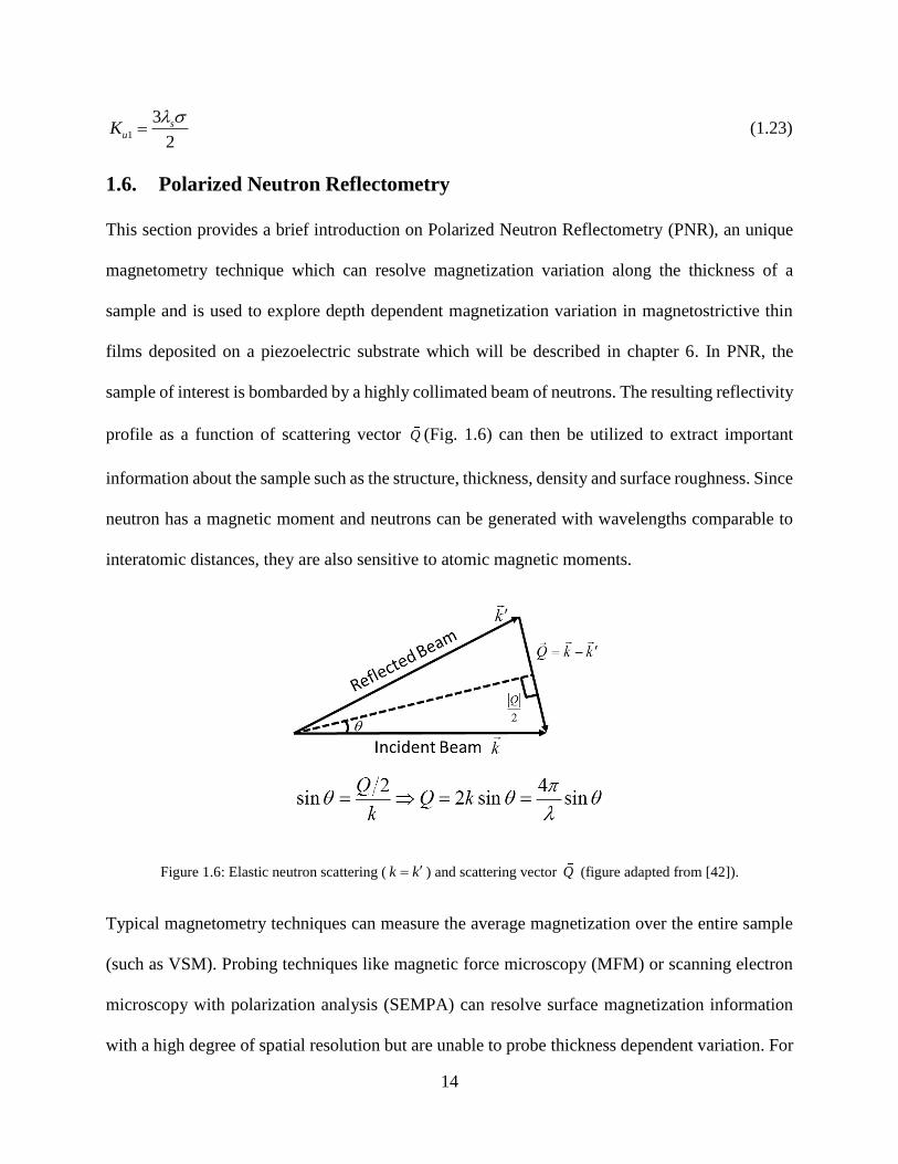
1.6. Polarized Neutron Reflectometry
This section provides a brief introduction on Polarized Neutron Reflectometry (PNR), an unique
magnetometry technique which can resolve magnetization variation along the thickness of a
sample and is used to explore depth dependent magnetization variation in magnetostrictive thin
films deposited on a piezoelectric substrate which will be described in chapter 6. In PNR, the
sample of interest is bombarded by a highly collimated beam of neutrons. The resulting reflectivity
profile as a function of scattering vector Q (Fig. 1.6) can then be utilized to extract important
information about the sample such as the structure, thickness, density and surface roughness. Since
neutron has a magnetic moment and neutrons can be generated with wavelengths comparable to
interatomic distances, they are also sensitive to atomic magnetic moments.
Figure 1.6: Elastic neutron scattering ( k k ) and scattering vector Q (figure adapted from [42]).
Typical magnetometry techniques can measure the average magnetization over the entire sample
(such as VSM). Probing techniques like magnetic force microscopy (MFM) or scanning electron
microscopy with polarization analysis (SEMPA) can resolve surface magnetization information
with a high degree of spatial resolution but are unable to probe thickness dependent variation. For
15
example, MFM measures the stray magnetic field emanating from a magnetic specimen from
which the average magnetization direction in the sample can be estimated. However, MFM cannot
resolve the depth dependent magnetization rotation in a 100 nm film. Polarized Neutron
reflectometry (PNR) is well suited for such depth dependent magnetization measurements. Like
other reflectometry techniques, the neutron reflectivity is sensitive to changes in the scattering
potential (can be pictured as equivalent to refractive index in optical reflectometry) along the
depth/thickness of the sample. Different materials and magnetization states present the incident
neutron beam with different scattering potentials. By measuring the specular reflectivity (coherent
elastic scattering) as a function of the wavevector transfer/scattering vector, the average in-plane
magnetization depth profile can be derived by fitting the obtained reflectivity data using
mathematical models.
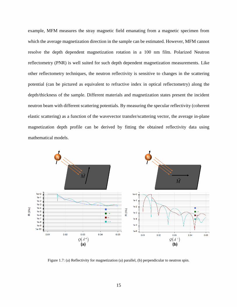
Figure 1.7: (a) Reflectivity for magnetization (a) parallel, (b) perpendicular to neutron spin.

16
The scattering of spin polarized neutron by the magnetization of the material can be divided into
two types, 1) spin flip (SF) scattering and 2) non-spin flip (NSF) scattering. If we denote the
neutron up-spin as “+” and down spin as “-”, there can be four different combination of the input
and output neutron spin, “++”, “--” which are NSF scattering and “+-”, “-+” which are SF
scattering, where the first sign denotes incident and the second sign denotes reflected neutron spin.
Fig. 1.7 shows neutron reflectivity for two situations in a PMN-PT/Ta(10nm)/Co(60nm) sample.
Only NSF scattering (“++” and “--”) are present and they are split when the in-plane component
of the magnetization vector is parallel to the neutron spin (Fig. 1.7.a). The SF scatterings are very
small and out of range in the figure. Fig. 1.7.b shows the reflectivity profile when the in-plane
component of the magnetization vector is perpendicular to the neutron spin. Here, both SF and
NSF scattering are present and the splitting between the two NSF scatterings has vanished. The
two NSF scatterings and the two SF scatterings are overlapping in this figure.
1.7. Dissertation Outline
This work investigates strain induced effects on magnetization, magnetization dynamics and
switching mechanism of nanomagnetic devices for Boolean and non-Boolean computing
applications. Chapter 2 discusses the effect of nanomagnet geometry on the speed, reliability and
energy dissipation of dipole coupled nanomagnetic logic (DC-NML). A scalable magnetic logic
wire using circular magnetic nanodots is proposed and numerical simulation using single domain
LLG approximation is presented in chapter 3. This chapter also briefly describes experiments
performed by our collaborators to support the theoretically proposed paradigm. The effect of
nanomagnet size on the coherence/incoherence of strain induced switching dynamics and
consequences of incoherent switching on the reliability of DC-NML are presented in chapter 4.
Chapter 5 includes the design and simulation of a straintronic magneto-tunneling junction device
17
for Ternary Content Addressable Memory (TCAM) application. Chapter 6 explores variation in
strain transfer and magnetization orientation along the thickness of a magnetostrictive cobalt thin
film on a PMN-PT substrate. Chapter 7 summarizes the thesis and proposes future research
directions with preliminary experimental work and future plan to achieve low voltage local strain
induced clocking on a PZT thin film.
18
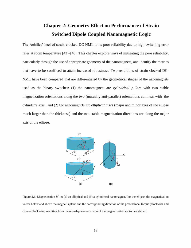
Chapter 2: Geometry Effect on Performance of Strain
Switched Dipole Coupled Nanomagnetic Logic
The Achilles’ heel of strain-clocked DC-NML is its poor reliability due to high switching error
rates at room temperature [43]–[46]. This chapter explore ways of mitigating the poor reliability,
particularly through the use of appropriate geometry of the nanomagnets, and identify the metrics
that have to be sacrificed to attain increased robustness. Two renditions of strain-clocked DC-
NML have been compared that are differentiated by the geometrical shapes of the nanomagnets
used as the binary switches: (1) the nanomagnets are cylindrical pillars with two stable
magnetization orientations along the two (mutually anti-parallel) orientations collinear with the
cylinder’s axis , and (2) the nanomagnets are elliptical discs (major and minor axes of the ellipse
much larger than the thickness) and the two stable magnetization directions are along the major
axis of the ellipse.
Figure 2.1. Magnetization �⃗⃗� in: (a) an elliptical and (b) a cylindrical nanomagnet. For the ellipse, the magnetization
vector below and above the magnet’s plane and the corresponding direction of the precessional torque (clockwise and
counterclockwise) resulting from the out-of-plane excursion of the magnetization vector are shown.
19
DC-NML of the latter variety (elliptical discs) is error-prone owing to the effect of the magnet
geometry on switching dynamics. This can be understood by looking at the illustration in Figure
2.1.a where the magnetization vector is represented in spherical coordinates with polar angle θ and
azimuthal angle φ. The polar angle θ is a measure of the out-of-plane excursion of the
magnetization vector; 𝜃<900and 𝜃>900 respectively imply that the magnetization is above/below
the plane of the magnet. Whenever the magnetization vector leaves the magnet’s plane during
switching, its out-of-plane component produces a demagnetization field in the out-of-plane
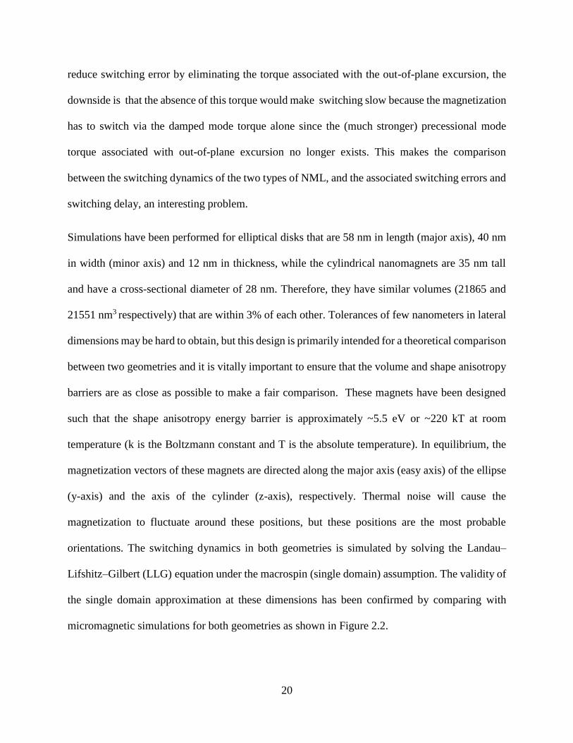
direction which generates a torque on the magnetization which either assists or hinders switching
depending on whether the magnetization vector is above or below the plane of the magnet (x-y
plane) [47]. Failure to switch will constitute an “error”. If there are neighboring magnets that
interact with the test magnet via dipole coupling, then the resulting dipole field can be utilized to
counter the hindering torque at least partially and improve the switching error rate. However, the
efficacy of this strategy may be limited by geometric constraints such the minimum allowable
separation between neighboring magnets (which determines the dipole coupling strength) and the
spread in the out-of-plane excursion of the magnetization vector at the operating temperature.
Limiting the out-of-plane excursion by judicious choice of nanomagnet geometry therefore
appears to be an appropriate route to reducing the frequency of error or probability of error.
Cylindrical nanomagnet shown in Figure 2.1.b have a geometry that can quench or eliminate the
offending precessional torque. The cylinder's axis is made the easy magnetization direction by
making the ratio of the cylinder’s height to diameter larger than 0.91 [48]. When the magnetization
is switched from the "up" (𝜃=0°) to the "down"(𝜃 = 180°) state, there is no "out-of-plane" or "in-
plane" direction perpendicular to the cylinder axis since the cross-section is circular and therefore
perfectly symmetric in the plane perpendicular to the cylinder’s axis. While this could potentially
20
reduce switching error by eliminating the torque associated with the out-of-plane excursion, the
downside is that the absence of this torque would make switching slow because the magnetization
has to switch via the damped mode torque alone since the (much stronger) precessional mode
torque associated with out-of-plane excursion no longer exists. This makes the comparison
between the switching dynamics of the two types of NML, and the associated switching errors and
switching delay, an interesting problem.
Simulations have been performed for elliptical disks that are 58 nm in length (major axis), 40 nm
in width (minor axis) and 12 nm in thickness, while the cylindrical nanomagnets are 35 nm tall
and have a cross-sectional diameter of 28 nm. Therefore, they have similar volumes (21865 and
21551 nm3 respectively) that are within 3% of each other. Tolerances of few nanometers in lateral
dimensions may be hard to obtain, but this design is primarily intended for a theoretical comparison
between two geometries and it is vitally important to ensure that the volume and shape anisotropy
barriers are as close as possible to make a fair comparison. These magnets have been designed
such that the shape anisotropy energy barrier is approximately ~5.5 eV or ~220 kT at room
temperature (k is the Boltzmann constant and T is the absolute temperature). In equilibrium, the
magnetization vectors of these magnets are directed along the major axis (easy axis) of the ellipse
(y-axis) and the axis of the cylinder (z-axis), respectively. Thermal noise will cause the
magnetization to fluctuate around these positions, but these positions are the most probable
orientations. The switching dynamics in both geometries is simulated by solving the Landau–
Lifshitz–Gilbert (LLG) equation under the macrospin (single domain) assumption. The validity of
the single domain approximation at these dimensions has been confirmed by comparing with
micromagnetic simulations for both geometries as shown in Figure 2.2.
21
The switching time as well as the switching error probability for both geometries for varying dipole
strengths have been studied. An increase in dipole coupling energy (smaller separation between
the nanomagnets) would produce a higher effective field and make the switching faster in both
geometries. This corresponds to the steeper slope in the energy profile shown in Fig. 1.6.b. Further,
stronger dipole coupling introduces a larger asymmetry in the potential profile shown in Fig. 1.6
that improves the probability of switching to the correct state, even in the presence of thermal
noise. While the above behavior is expected for both geometries, the interesting question is how
the two geometries differ with respect to switching speed and error. This is discussed next after
briefly explaining the simulation conditions and procedures.
Figure 2.2. Comparison between magnetization dynamics predicted by micromagnetic simulations and single domain
LLG for (a) elliptical, (b) cylindrical nanomagnets.
2.1. Simulation Conditions: Stress Application
A compressive stress exactly equal to the critical stress is applied in the elliptical (44.28
MPa) and cylindrical (45.85 MPa) nanomagnets (see the caption of Fig. 1.6 for definition of the
term “critical stress”). Previous work from our group had shown that for a given dipole coupling,
the switching probability is highest (error probability least) when the stress applied is the critical
stress [43].

22
2.2. Switching Time Estimate
The switching trajectories and the corresponding switching times are random in the
presence of thermal noise. Because we are interested in the difference between the two geometries,
the following strategy has been adopted. Stochastic LLG simulations in the presence of thermal
noise has been performed to determine the thermal distribution of the magnetization vector around
a stable orientation, and randomly pick a starting point from this distribution. The stress pulse is
applied to kick the magnetization out of its initial stable orientation around = 900 and set it off
towards the intended final stable orientation around = 2700. The temporal evolution of the
magnetization orientation has been simulated and the time taken for the magnetization orientation
to reach close to =270° (the switching is deemed to have occurred if the deviation of the final
value 270° is within 1°) has been determined. This process is repeated to generate different
switching trajectories. The fraction of the trajectories that fail to reach close to = 2700 is the error
probability. A similar methodology is used for the cylinder case. In both cases, switching occurs
with highest probability because critical stress has been applied that just erodes the shape
anisotropy barrier and does not force the magnetization to orient close to the hard axis, and
thereafter makes the magnetization switch because of dipole coupling with the left neighbor (which
prefers anti-ferromagnetic ordering). The mean switching time is calculated by averaging over the
successful trajectories. We also find the longest switching time (from the slowest trajectory) to
assess the worst case scenario. The calculated energy dissipation includes the internal dissipation
in the magnet due to Gilbert damping and the (1/2)CV2 dissipation associated with charging the
capacitor C formed by the piezoelectric layer, with V being the voltage needed to produce the
electric fields in the piezoelectric to generate the stress.
23
In case of elliptic nanomagnets, the capacitance C is estimated assuming that two square
electrodes of side ~50 nm are used to apply the voltage over a PZT layer of thickness ~50 nm in
the manner of [18]. For applying stress to the cylindrical nanomagnet in the manner of [49], the
PZT matrix is assumed to be ~ 70 nm thick and the capacitor plate is square with side dimension
of ~70 nm.
2.3. Comparison between the Elliptical and Cylindrical Geometries In Terms
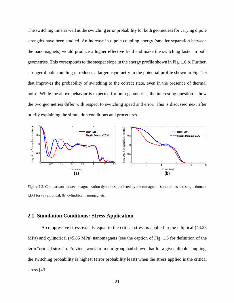
Of Switching Time or Switching Speed
Figure 2.3.a and Figure 2.3.b show the switching times for elliptical and cylindrical geometries
assuming comparable dipole coupling strengths. As expected, increased dipole coupling decreases
the switching time in both cases. However, at any given dipole coupling strength, the switching
time is ~10 to 50 times (1-2 orders of magnitude) longer for the cylindrical geometry compared to
the elliptical one. This highlights the critical role played by the switching geometry in determining
the switching speed and hence, ultimately, the clock speed in DC-NML.
Figure 2.3. Switching time vs. dipole energy (determined by the center-to-center separation between neighboring
nanomagnets) for (a) elliptical nanomagnets and (b) cylindrical nanomagnets.
In the case of the elliptical magnet, when the magnetization rotates anticlockwise (or clockwise),
the magnetization lifts out of the plane (or dips below the plane) [15, 20]. This produces a
magnetization component in the positive and negative z-direction, respectively, that leads to an
24
effective field in the negative or positive direction. This z-directed field increases the anticlockwise
(or clockwise) torque, thereby increasing the speed of the switching.
However, in the case of the cylindrical geometry, as the magnetization switches from ~00 to
~1800, the -component of motion does not produce any additional torque since the geometry is
completely symmetric with respect to . Hence, the switching is primarily via the damped mode
torque (unlike the elliptical geometry where the precessional mode torque plays a significant role
in the switching process). Since most materials have a small Gilbert damping factor α, the damped
mode torque is usually far weaker than the precessional mode torque. This explains the extremely
slow switching times in the cylindrical geometry and the difference with the elliptical geometry.
2.4. Switching Error Estimate
The switching error probabilities in Figure 2.4.a and Figure 2.4.b were estimated by performing
stochastic LLG simulations. The simulation was first run for 1 ns without applying any stress and
the distribution of the magnetization orientation around the stable easy direction was obtained.
Next, a switching trajectory was generated by solving (1.9) and (1.10). The starting point of this
trajectory (at time t = 0) was picked from the distribution generated in the previous step with the
corresponding weight. Thereafter, the stress was ramped up to the critical stress value for 1 ns,
held for a period of time as described in the legends of Fig 2.4 and then removed in a 1 ns
downward ramp. The system was given ~ 1 ns (ellipse) and ~27 ns (for the cylinder) to come to a
steady state. The relaxation time was determined by the time it took all the magnetization
trajectories to end up in one of the stable states. The fraction of the number of trajectories that had
not switched to the correct state constituted the switching error probability. For most cases,
100,000 trajectories were simulated at 300 K. However, in cases where we report error
probabilities of ~10-6, 10-7 and 10-8, the number of trajectories simulated was 1 million, 10 million
25
and 100 million, respectively. Because simulation of so many trajectories is time consuming, such
simulations were limited to a few cases where the dipole coupling strength was extremely high.
The 1 to 100 million simulations cases were performed only on the elliptical geometry as it is
computationally more tractable to do these simulations over a switching time ~10 ns as opposed
~several 100 ns needed for the cylindrical geometry.
Figure 2.4. (a) Representative stress profile. (b) and (c) Switching probability (PSW) vs. dipole coupling energy (or
equivalently center to center separation between neighboring nanomagnets) for (b) elliptical nanomagnets and (c)
cylindrical nanomagnets. The results are shown for two different switching times. Initial time before application of
stress, stress ramp up and stress ramp down times are fixed at 1 ns each. Final relaxation time, after stress in ramped
down, is 1 ns for ellipse and 27 ns for the cylinder. The stress hold times are 1 and 3 ns for the two ellipse cases and
70 ns and 270 ns for the two cylinder cases. The total time (ramp up, hold and ramp down, relaxation time) is indicated
on the figure legends.
2.5. Comparison between the Elliptical and Cylindrical Geometries in terms of
Switching Error
Fig. 2.4.b and Fig. 2.4.c respectively show the dynamic switching error vs. dipole coupling
energy (which is ultimately the internal energy dissipated) for the elliptical and circular geometry.
Despite the absence of the torque due to "out-of-plane" magnetization distribution in the
cylindrical geometry, the switching error is not any better than the elliptical case where the
detrimental effects of the "out-of-plane" magnetization distribution is successfully countered by
26
strong dipole coupling. The torque produced by the out-of-plane excursion of the magnetization
orientation significantly shortens the switching time in the elliptical geometry but does not increase
the switching error probability in the range of dipole energies and error rates we study. If the dipole
coupling strength had been weaker, the elliptical geometry would surely have been more error-
prone than the cylindrical geometry because of the effect of the out-of-plane magnetization
distribution, but in the limit of strong dipole coupling, the effect of the out-of-plane magnetization
distribution is diminished to the point where the difference between the two geometries become
nearly imperceptible.
Clearly, stronger dipole coupling will reduce the error rates in dipole coupled nanomagnetic
logic. However, the dipole coupling energy cannot be increased arbitrarily; it must never exceed
the shape anisotropy energy barrier in the nanomagnets since that would then align their
magnetizations along the minor axes of the ellipses (the line joining their centers) resulting in
ferromagnetic ordering that does not implement the NOT logic functionality. Therefore, increasing
the dipole coupling necessitates increasing the shape anisotropy energy barrier as well. For safe
operation, the latter should be maintained at somewhat above the maximum dipole coupling
energy. In our case, it was approximately ~220 kT (~ 5.5 eV).
So, it is clear that increased dipole coupling strength results in lower error probability and faster
switching, but obviously at the expense of higher energy dissipation since stronger dipole coupling
causes larger dissipation [15]. Comparable error probabilities with comparable energy dissipation
have been found but much faster switching speed for the elliptical geometry compared to the
cylindrical geometry for the dipole coupling strengths considered. Thus, the elliptical geometry
produces a very favorable energy-delay product for a given error rate, compared to the cylindrical
geometry, as shown in Figure 2.6.a. From the case with 100 million simulations, it is estimated
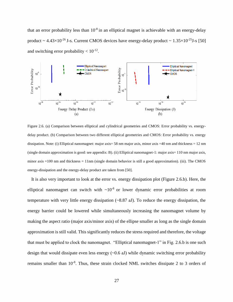
27
that an error probability less than 10-8 in an elliptical magnet is achievable with an energy-delay
product ~ 4.43×10⁻²⁶ J-s. Current CMOS devices have energy-delay product ~ 1.35×10⁻²⁵J-s [50]
and switching error probability < 10-12.
Figure 2.6. (a) Comparison between elliptical and cylindrical geometries and CMOS: Error probability vs. energy-
delay product. (b) Comparison between two different elliptical geometries and CMOS: Error probability vs. energy
dissipation. Note: (i) Elliptical nanomagnet: major axis= 58 nm major axis, minor axis =40 nm and thickness = 12 nm
(single domain approximation is good: see appendix: B). (ii) Elliptical nanomagnet-1: major axis= 110 nm major axis,
minor axis =100 nm and thickness = 11nm (single domain behavior is still a good approximation). (iii). The CMOS
energy-dissipation and the energy-delay product are taken from [50].
It is also very important to look at the error vs. energy dissipation plot (Figure 2.6.b). Here, the
elliptical nanomagnet can switch with ~10-8 or lower dynamic error probabilities at room
temperature with very little energy dissipation (~8.87 aJ). To reduce the energy dissipation, the
energy barrier could be lowered while simultaneously increasing the nanomagnet volume by
making the aspect ratio (major axis/minor axis) of the ellipse smaller as long as the single domain
approximation is still valid. This significantly reduces the stress required and therefore, the voltage
that must be applied to clock the nanomagnet. “Elliptical nanomagnet-1” in Fig. 2.6.b is one such
design that would dissipate even less energy (~0.6 aJ) while dynamic switching error probability
remains smaller than 10-8. Thus, these strain clocked NML switches dissipate 2 to 3 orders of
28
magnitude less energy than a state-of-the-art CMOS switch which dissipates ~440 aJ. However,
the CMOS switch is also less error prone with dynamic switching error probability typically < 10-
12.
2.6. Conclusion
In general, a CMOS switch may outperform dipole coupled nanomagnetic logic in switching speed
and error rates, but it is usually more dissipative and most importantly, it is volatile. The
straintronic NOT gate studied here is non-volatile and can achieve switching error rates of ~10-8
with optimized design while dissipating only 0.6 aJ/bit. This error rate is remarkable for
nanomagnetic logic but still does not meet the stringent requirement for general purpose Boolean
logic. Moreover, these theoretical error estimates assume that there are no fabrication defects such
as variations in nanomagnet dimensions and misalignments between nanomagnets which can cause
additional errors. It should be noted that these are not easily quantifiable and hence not addressed
here. This chapter focuses only on intrinsic errors caused by thermal noise to estimate a theoretical
limit on the reliability of dynamic switching. The nanomagnets are assumed to be nano-patterned
Terfenol-D, which still has not been demonstrated experimentally. In practice, nanomagnets for
straintronic devices are fabricated using low magnetostriction materials such as Nickel and Cobalt,
which are more susceptive to switching errors due to lithographic variations. Their strain induced
effective magnetic fields are very low compared to Terfenol-D and therefore, small changes in
shape anisotropy due to variations in dimensions can have a large effect.
However, with the rise of embedded electronics and internet of things, there exists a plethora of
niche applications where energy is a premium, 10-8 error probability can be tolerated and clock
speeds ~ 100 MHz are sufficient. There, dipole coupled nanomagnetic computing schemes,

29
clocked in an energy efficient manner (for example with strain) coupled with their inherent non-
volatility, may steal a march over traditional CMOS-based implementations.
This work has been published in IEEE Transactions of Electron Devices [9].
30
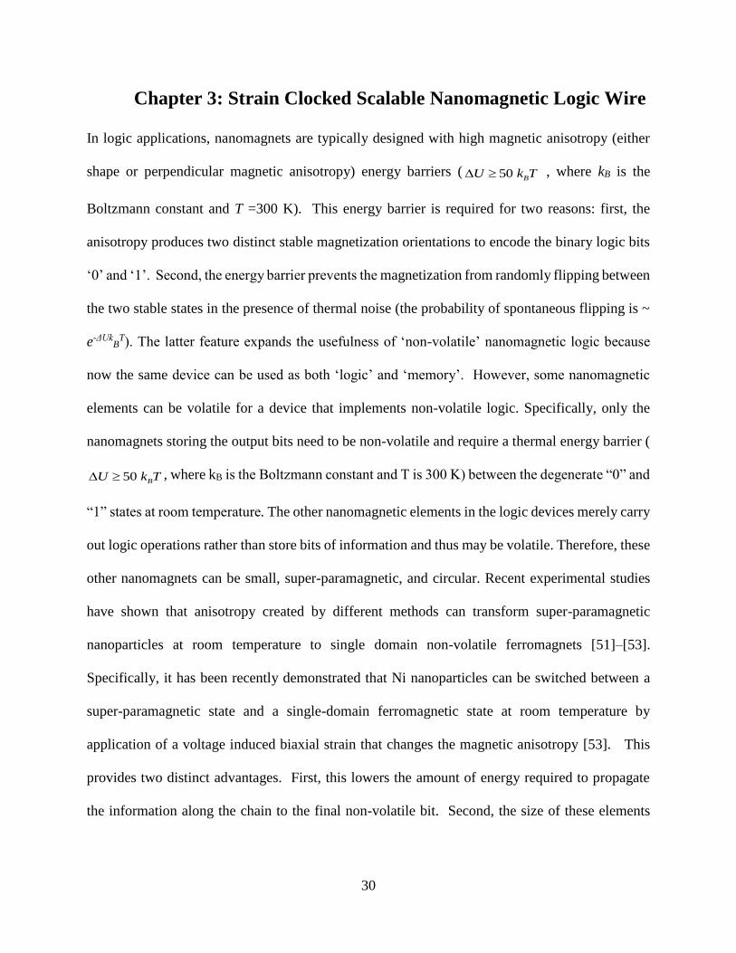
Chapter 3: Strain Clocked Scalable Nanomagnetic Logic Wire
In logic applications, nanomagnets are typically designed with high magnetic anisotropy (either
shape or perpendicular magnetic anisotropy) energy barriers ( 50 BU k T , where kB is the
Boltzmann constant and T =300 K). This energy barrier is required for two reasons: first, the
anisotropy produces two distinct stable magnetization orientations to encode the binary logic bits
‘0’ and ‘1’. Second, the energy barrier prevents the magnetization from randomly flipping between
the two stable states in the presence of thermal noise (the probability of spontaneous flipping is ~
e-ΔUkB
T). The latter feature expands the usefulness of ‘non-volatile’ nanomagnetic logic because
now the same device can be used as both ‘logic’ and ‘memory’. However, some nanomagnetic
elements can be volatile for a device that implements non-volatile logic. Specifically, only the
nanomagnets storing the output bits need to be non-volatile and require a thermal energy barrier (
50 BU k T , where kB is the Boltzmann constant and T is 300 K) between the degenerate “0” and
“1” states at room temperature. The other nanomagnetic elements in the logic devices merely carry
out logic operations rather than store bits of information and thus may be volatile. Therefore, these
other nanomagnets can be small, super-paramagnetic, and circular. Recent experimental studies
have shown that anisotropy created by different methods can transform super-paramagnetic
nanoparticles at room temperature to single domain non-volatile ferromagnets [51]–[53].
Specifically, it has been recently demonstrated that Ni nanoparticles can be switched between a
super-paramagnetic state and a single-domain ferromagnetic state at room temperature by
application of a voltage induced biaxial strain that changes the magnetic anisotropy [53]. This
provides two distinct advantages. First, this lowers the amount of energy required to propagate
the information along the chain to the final non-volatile bit. Second, the size of these elements
31
can be made ultra-small to increase processing density. This results in an extremely energy
efficient nanomagnetic logic device that improves scalability to smaller feature sizes.
Figure 3.1. Implementation of a logic wire. (a) A multiferroic circular nanomagnet with diameter of 100 nm and
thickness of 12 nm, and (b) Chain of dipole coupled nanomagnets with center to center separation of "R". The
nanomagnets are delineated on top of a PZT layer and can be clocked sequentially using a local clocking scheme that
generates local stress only under the selected nanomagnet [18].
A critical component of the dipole-coupled nanomagnetic logic systems is a “binary wire” that
propagates a logic bit unidirectionally from one end of the wire to the other [2], [6], [8], [37], [24],
[38]. This chapter presents theoretical simulations of a binary wire implemented with a linear array
of dipole-coupled circular nanomagnets subjected to room-temperature thermal noise. In this
simulation, voltage induced Bennett clocking [38] of the nanomagnets is achieved with strain
produced by a piezoelectric thin film deposited onto a silicon substrate as shown in Figure 3.1.
Here voltage is applied to electrode pairs to overcome the substrate clamping issues imposed on a
thin film piezoelectric (~500 nm or less) as proposed by Cui et al. [18] to generate a bi-axial strain
that is transferred to the nanomagnet.1. Here voltage is applied to electrode pairs to overcome the
substrate clamping issues imposed on a thin film piezoelectric (~500 nm or less) as proposed by
Cui et al. [18] to generate a bi-axial strain that is transferred to the nanomagnet. By sequentially
32
applying a voltage, propagation of the information encoded in the magnetic moments of the
nanomagnetic wire is achieved.
Further, the ability to induce bistability with magnetic anisotropy induced by strain in dipole
coupled circular Ni nanodots of 100 nanometer diameter deposited on a PMN-PT substrate has
been experimentally demonstrated by collaborators which will also be briefly discussed. Note that
these experiments use global clocking as the tests are performed on a bulk PMN-PT substrate
rather than thin film PZT. The strain mediated voltage control of magnetic anisotropy in circular
nanomagnets may spawn a new genre of efficient nanomagnetic logic hardware implemented with
ultra-small circular super-paramagnetic structures.
3.1. Information Propagation in an Array of Circular Nanomagnets with
Thermal Noise
Here, information propagation without stress and then with sequential application of stress are
presented to show how the latter in necessary to propagate information in circular nanomagnets in
the presence of thermal noise. The binary wire consists of a linear array of dipole coupled
nanomagnets. The stochastic magnetization dynamics of these nanomagnets in the array under the
influence of dipole fields and stress was simulated using the Landau-Lifshitz-Gilbert (LLG)
equation under single domain approximation.
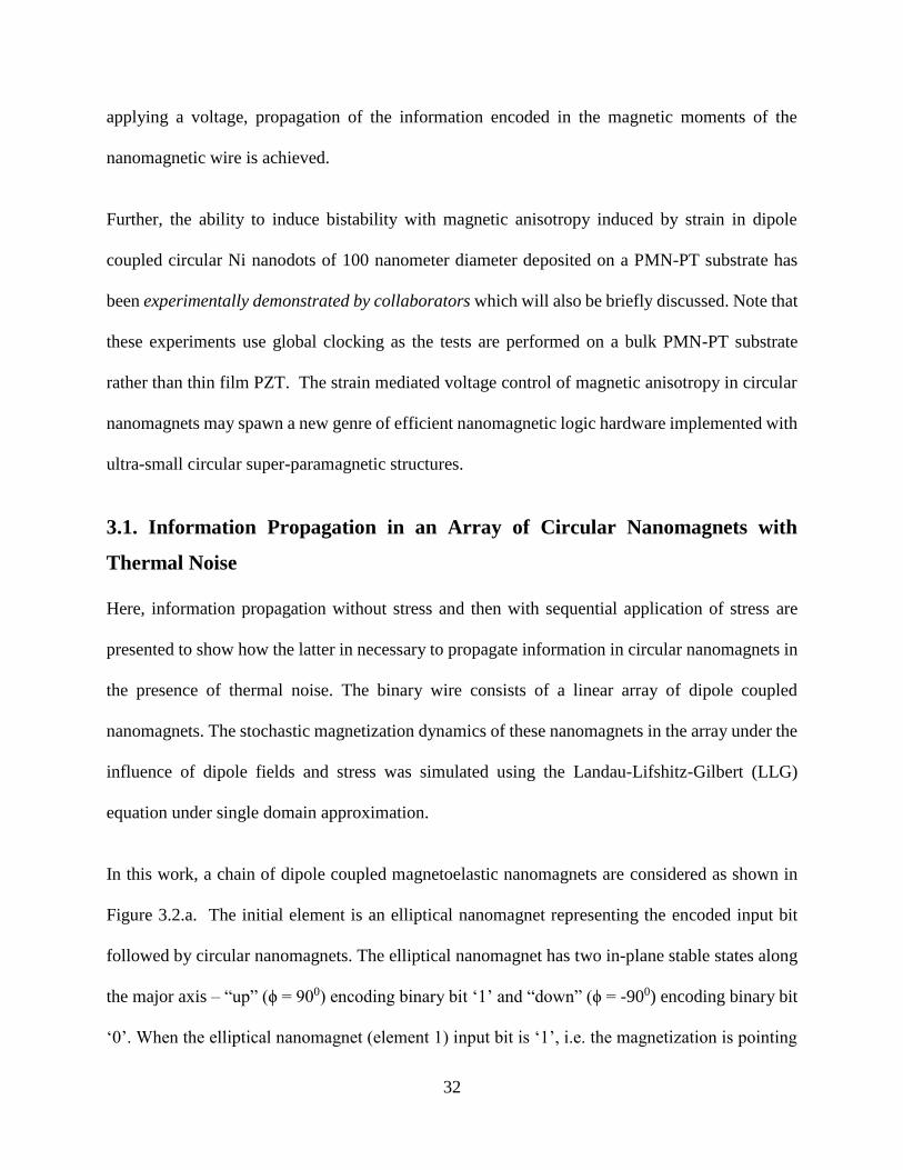
In this work, a chain of dipole coupled magnetoelastic nanomagnets are considered as shown in
Figure 3.2.a. The initial element is an elliptical nanomagnet representing the encoded input bit
followed by circular nanomagnets. The elliptical nanomagnet has two in-plane stable states along
the major axis – “up” (ϕ = 900) encoding binary bit ‘1’ and “down” (ϕ = -900) encoding binary bit
‘0’. When the elliptical nanomagnet (element 1) input bit is ‘1’, i.e. the magnetization is pointing
33
“up” (ϕ =90o), its magnetic dipole influences the next circular nanomagnet (element 2) to point
“down” (ϕ = -900). Furthermore, dipole-dipole coupling between element 2 and the next circular
nanomagnet (element 3) causes the third element to rotate towards the down (ϕ = -900) horizontal.
Figure 3.2. Information propagation in a binary wire composed of circular nanomagnets. (a) Schematic view of dipole
coupled circular nanomagnets forming a “logic wire” preceded by a high shape-anisotropy nanomagnet acting as the
input bit host. (b) Fluctuations of nanomagnet’s in-plane magnetization orientation about the mean orientation vs.
time in the absence of stress. (c) Sequential clocking of the circular nanomagnets with compressive mechanical stress.
(d) In-plane magnetization dynamics of dipole coupled nanomagnets versus time, showing that stress promotes “logic
restoration” or near “up” or near “down” orientation of the magnetization in each nanomagnet.
As the number of circular nanomagnets increases in the line, the dipole-dipole dictated by the first
elliptical nanomagnetic producing the anti-parallel vertical ordering (“up”, “down”, “up”, “down”
and so on) gives way to dipole-dipole coupling present between the circular nanomagnetic that
dictates a horizontal orientation (parallel alignment) of the magnetization along the axis of the
34
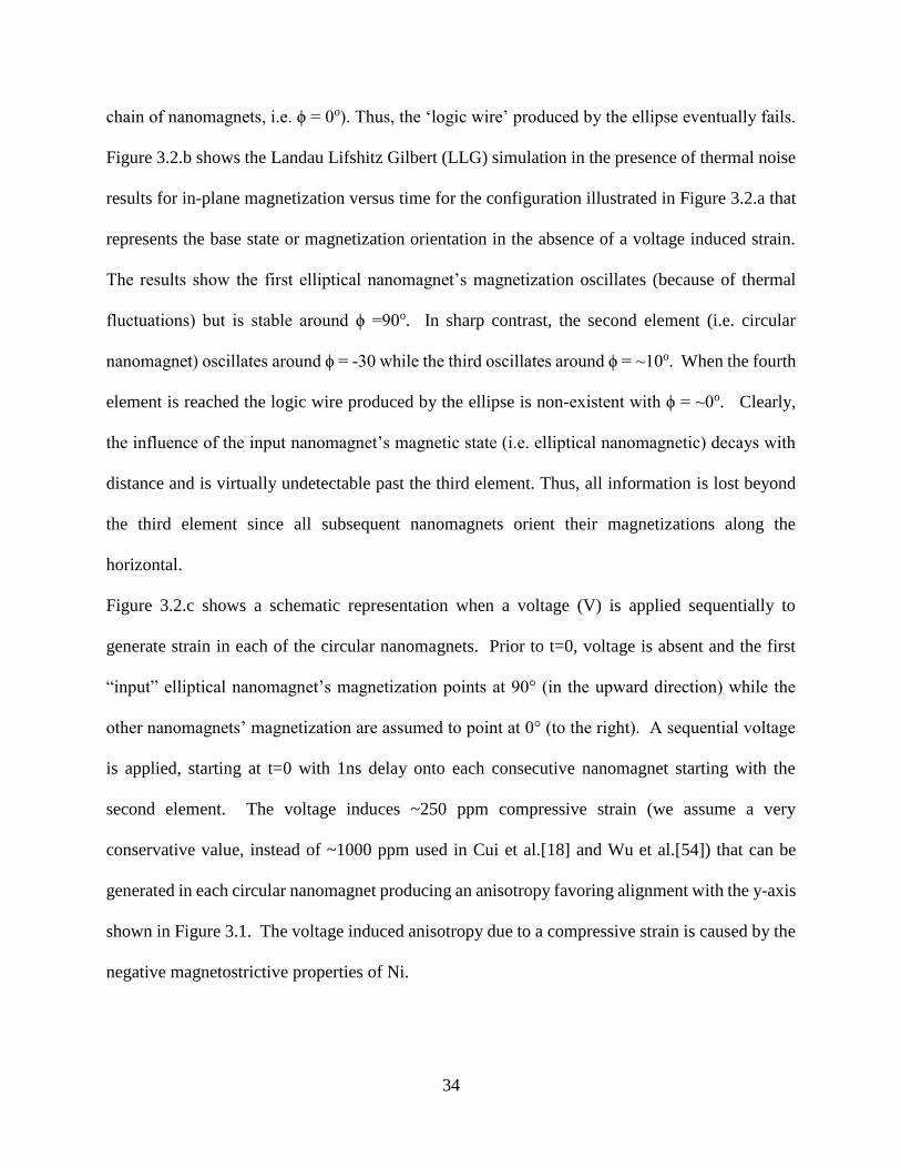
chain of nanomagnets, i.e. ϕ = 0o). Thus, the ‘logic wire’ produced by the ellipse eventually fails.
Figure 3.2.b shows the Landau Lifshitz Gilbert (LLG) simulation in the presence of thermal noise
results for in-plane magnetization versus time for the configuration illustrated in Figure 3.2.a that
represents the base state or magnetization orientation in the absence of a voltage induced strain.
The results show the first elliptical nanomagnet’s magnetization oscillates (because of thermal
fluctuations) but is stable around ϕ =90o. In sharp contrast, the second element (i.e. circular
nanomagnet) oscillates around ϕ = -30 while the third oscillates around ϕ = ~10o. When the fourth
element is reached the logic wire produced by the ellipse is non-existent with ϕ = ~0o. Clearly,
the influence of the input nanomagnet’s magnetic state (i.e. elliptical nanomagnetic) decays with
distance and is virtually undetectable past the third element. Thus, all information is lost beyond
the third element since all subsequent nanomagnets orient their magnetizations along the
horizontal.
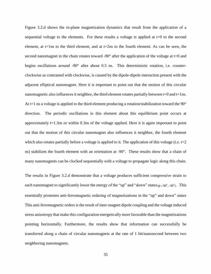
Figure 3.2.c shows a schematic representation when a voltage (V) is applied sequentially to
generate strain in each of the circular nanomagnets. Prior to t=0, voltage is absent and the first
“input” elliptical nanomagnet’s magnetization points at 90° (in the upward direction) while the
other nanomagnets’ magnetization are assumed to point at 0° (to the right). A sequential voltage
is applied, starting at t=0 with 1ns delay onto each consecutive nanomagnet starting with the
second element. The voltage induces ~250 ppm compressive strain (we assume a very
conservative value, instead of ~1000 ppm used in Cui et al.[18] and Wu et al.[54]) that can be
generated in each circular nanomagnet producing an anisotropy favoring alignment with the y-axis
shown in Figure 3.1. The voltage induced anisotropy due to a compressive strain is caused by the
negative magnetostrictive properties of Ni.
35
Figure 3.2.d shows the in-plane magnetization dynamics that result from the application of a
sequential voltage to the elements. For these results a voltage is applied at t=0 to the second
element, at t=1ns to the third element, and at t=2ns to the fourth element. As can be seen, the
second nanomagnet in the chain rotates toward -90° after the application of the voltage at t=0 and
begins oscillations around -90° after about 0.5 ns. This deterministic rotation, i.e. counter-
clockwise as contrasted with clockwise, is caused by the dipole-dipole interaction present with the
adjacent elliptical nanomagnet. Here it is important to point out that the motion of this circular
nanomagnetic also influences it neighbor, the third element rotates partially between t=0 and t=1ns.
At t=1 ns a voltage is applied to the third element producing a rotation/stabilization toward the 90°
direction. The periodic oscillations in this element about this equilibrium point occurs at
approximately t=1.3ns or within 0.3ns of the voltage applied. Here it is again important to point
out that the motion of this circular nanomagnet also influences it neighbor, the fourth element
which also rotates partially before a voltage is applied to it. The application of this voltage (i.e. t=2
ns) stabilizes the fourth element with an orientation at -90°. These results show that a chain of
many nanomagnets can be clocked sequentially with a voltage to propagate logic along this chain.
The results in Figure 3.2.d demonstrate that a voltage produces sufficient compressive strain to
each nanomagnet to significantly lower the energy of the “up” and “down” states 0 0( 90 , 90 ) . This
essentially promotes anti-ferromagnetic ordering of magnetizations in the “up” and down” states
This anti-ferromagnetic orders is the result of inter-magnet dipole coupling and the voltage induced
stress anisotropy that make this configuration energetically more favorable than the magnetizations
pointing horizontally. Furthermore, the results show that information can successfully be
transferred along a chain of circular nanomagnets at the rate of 1 bit/nanosecond between two
neighboring nanomagnets.

36
An important consideration in any logic scheme, is the reliability with which information is
propagated in the presence of thermal noise. Magnetization dynamics in the presence of thermal
noise have been simulated 105 times at each pitch (center-center distance) and the number of times
propagation fails have been counted. We model failure owing to disruption of the switching due
to thermal noise and not owing to other potential spoilers such as pinning of magnetization by
defects or misalignment (magnet centers are not on the same straight line). Figure 3.3 shows the
switching probability of the chain of circular nanomagnets as a function of the center-center
distance (pitch) between the 100 nm diameter and 12 nm thick circular nanomagnets clocked with
a strain of ~250 micro-strain. Clearly, an increase in pitch leads to lower dipole coupling, making
it easier for thermal noise to cause disruptions in the magnetization switching process. This leads
to decreased switching probability with increasing pitch. For one particular case, the design
presented in this work (pitch ~150 nm), there was no switching error in 106 simulations indicating
the error probability is smaller than 10-6.
Figure 3.3. Probability of switching in circular nanomagnets for different dipole coupling under the effect of thermal
noise. The coupling increases with decreasing pitch (center-center) separation resulting in increased switching
reliability.
37
The numerical simulations assume two mechanisms dominate the magnetization reorientation.
These two effects are (1) dipole coupling between nanomagnets and (2) stress induced magnetic
anisotropy through the magnetoelastic effect. To demonstrate that these are the two dominant
mechanisms a series of experiments were designed to establish the dipole effect and stress induced
uniaxial magnetic anisotropy in the same chain of nanomagnets. These effects can be quantified
by measuring the averaged M-H curves of an ensemble of nanomagnets and focusing on a large
pitch array, a small pitch array (dipole coupled) without stress and a small pitch array subjected to
stress. By measuring the remanence changes along select directions specific conclusions can be
drawn about the relative magnitudes and the ability to control dipole coupling in the proposed
logic device supporting the analytical conclusions. These results are discussed below.
3.2. Experimental Demonstration
(Performed by collaborators, Wei-Yang Sun, P. Nordeen, A.C. Chavez, G.P. Carman, Department
of Mechanical and Aerospace Engineering, Univ. of California, Los Angeles, CA 90095.)
Two different samples were tested consisting of Nickel circular (100nm) nanodot arrays patterned
on a 10mm x 10mm x 0.5mm single crystal (011) PMN-PT substrate sourced from TRS
Technologies, Inc., USA. The arrays are 1x1 mm and isolated from each other with a 2mm
separation as shown in Figure 3.4.a. The [100] in-plane crystallographic axis of the PMN-PT
substrate is aligned with the sample’s y-direction while the [011] in-plane crystallographic axis is
aligned with the x-direction. The nanodot pitch along the y-direction is 500nm for all arrays while
the nanodot pitch along the x-direction is 250nm and 150nm for arrays 1 and 2, respectively.
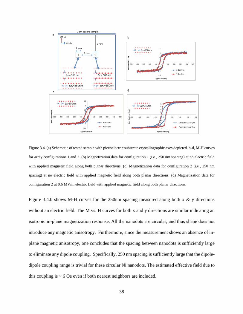
38
Figure 3.4. (a) Schematic of tested sample with piezoelectric substrate crystallographic axes depicted. b-d, M-H curves
for array configurations 1 and 2. (b) Magnetization data for configuration 1 (i.e., 250 nm spacing) at no electric field
with applied magnetic field along both planar directions. (c) Magnetization data for configuration 2 (i.e., 150 nm
spacing) at no electric field with applied magnetic field along both planar directions. (d) Magnetization data for
configuration 2 at 0.6 MV/m electric field with applied magnetic field along both planar directions.
Figure 3.4.b shows M-H curves for the 250nm spacing measured along both x & y directions
without an electric field. The M vs. H curves for both x and y directions are similar indicating an
isotropic in-plane magnetization response. All the nanodots are circular, and thus shape does not
introduce any magnetic anisotropy. Furthermore, since the measurement shows an absence of in-
plane magnetic anisotropy, one concludes that the spacing between nanodots is sufficiently large
to eliminate any dipole coupling. Specifically, 250 nm spacing is sufficiently large that the dipole-
dipole coupling range is trivial for these circular Ni nanodots. The estimated effective field due to
this coupling is ~ 6 Oe even if both nearest neighbors are included.
39
Figure 3.4.c shows M-H loops measured along both x and y directions for the 150 nm spaced array
without an electric field. When contrasting these measurements to those of Figure 3.4.b for the 250
nm spaced array, distinct similarities and differences are noted. First, there is a similarity in the
Mr values measured in the x direction, in particular they are approximately 0.8. Second, there is a
dissimilarity in the Mr values measured in the y direction; specifically the Mr for the 150 nm array
is 0.5 while for the 250 nm array it is 0.8. The results for the 150 nm spacing clearly shows the
presence of dipole-dipole coupling. Specifically dipole-dipole coupling along the y direction
should produce anti-parallel magnetization alignment reducing the measured Mr values along the
y direction. Figure 3.4.d shows M-H curves for the 150 nm spaced array with a 0.6 MV/m electric
field applied. The results show a distinct change in the M-H curves with the applied electric field
as contrasted with the results without an electric field shown in Figure 3.4.c. Specifically, without
an electric field the remnant magnetization in the x-direction is 0.8, but when a field is applied the
remanence decreases to approximately 0.5. The remanence decreases as the easy axis is now being
established along an axis perpendicular to the x-axis array. This causes the easy magnetization
direction to rotate toward the y-axis and away from x-axis, in spite of the dipole coupling. A change
in Mr occurs for the y-direction as well. However, the remanence increases from 0.5 to about 0.8
with an applied electric field. The remanence increase in the y-direction is surprising given the
dipole coupling favors an anti-parallel state in the y direction. However, for this configuration the
stress induced magnetic anisotropy is sufficiently large to mask the dipole effect and ensure the
nanomagnets magnetization remains along the y-direction even after the magnetic field is
withdrawn. This result clearly confirms that the magnetic easy axis of the nanomagnet is
established along the y-direction when an electric field is applied. This change is attributed to the
voltage induced magnetoelastic effect. Since Ni is negatively magnetostrictive, the magnetoelastic
40
response of the nanostructures causes the magnetization to favor alignment with the axis of
compression implying that the chain axis is magnetically harder. It has also been established that
the magnetoelastic energy is sufficiently larger than the dipole-dipole coupling that favors anti-
parallel alignment in the y-direction and parallel alignment in the x-direction.
3.3. Conclusion
The simulations and the experiments together demonstrate the feasibility of using circular
magnetostrictive nanomagnets clocked with strain to propagate information. It has further been
estimated theoretically that information can be transmitted along a circular nanomagnet chain
clocked with stress with high reliability (error < 10-6 m) considering there are no defects that can
pin the magnetization in such magnets. It can also be extremely low energy < 1aJ/bit, provided it
is implemented on thin film PZT. More importantly, this could provide a path to the ultimate
scaling of nanomagnetic devices to implement Boolean operation and propagate logic at lateral
dimensions below 20 nm, along with very little energy dissipation. However, the key to such
scaling experimentally is to develop techniques to successfully nano-pattern high magnetostrictive
materials like Terfenol-D while also having sufficient control over lithographic variations,
misalignments and imperfections can be controlled at these scales.
This work has been performed in collaboration with Professor Greg Carman and his graduate
students Wei-Yang Sun, P. Nordeen and A.C. Chavez at Department of Mechanical and Aerospace
Engineering, University of California, Los Angeles. They have performed the experimental part
of this work (section 3.2) including sample preparation and MOKE measurements. This work has
been published in Nanotechnology [55].
41
Chapter 4: Dynamic Error in Strain-Induced Magnetization
Reversal of Nanomagnets Due to Incoherent Switching and
Formation of Metastable States: A Size-Dependent Study
This chapter presents micromagnetic simulations using MuMax3 [40] for a comprehensive
understanding of the strain induced switching dynamics i.e. coherency/incoherency of the
switching process, its dependence on the nanomagnet dimension, and its influence on the switching
reliability and energy dissipation. In this study, elliptical disk nanomagnets of three different
dimensions have been simulated while keeping the aspect ratio (ratio of major to minor axis to the
thickness) constant. A constant aspect ratio ensures constant demagnetizing factors across all
dimensions, so the outcome of the simulations will be solely affected by the nanomagnet size. The
simulated nanomagnet dimensions are listed in Table 4.1, where "length" is the dimension of the
major axis and "width" is that of the minor axis.
Table 4.1: Simulated nanomagnet dimensions.
Nanomagnet Length (nm) Width (nm) Thickness (nm)
Small 60 40 6
Intermediate 120 80 12
Large 150 120 15
To observe the effect of incoherent reversal in strain induced switching, we use dipole coupling as
shown in Figure 4.1.a to ensure complete magnetization reversal since strain, by itself, can produce
no more than 90º rotation. This scheme, where a dipole field is utilized to implement the complete
reversal under stress, actually represents a very important case, namely the operation of a NOT
gate. The neighboring hard nanomagnet’s magnetization represents the input bit written into it by
42
some external agent (e.g. a local magnetic field or spin polarized current). The magnetization of
the test (soft) nanomagnet represents the output bit. Dipole coupling between the two nanomagnets
will prefer to align their magnetizations in mutually anti-parallel orientations, making the output
bit the logic complement of the input bit (NOT operation).
Figure 4.1. (a) Stress induced magnetization reversal in the presence of a dipole field caused by a neighboring (left)
hard nanomagnet with fixed magnetization. (b) Schematic diagram of the switching set up. A nanomagnet is delineated
on top of a piezoelectric substrate and a potential applied between two shorted top electrodes and a bottom electrode
generates stress in the nanomagnet inducing its magnetization to rotate [18].
However, when the input bit is altered, the output bit does not respond and flip automatically to
complete the NOT operation since dipole coupling is usually not strong enough to overcome the
shape anisotropy of the test nanomagnet and cause magnetization reversal. Therefore, stress is
applied to the test nanomagnet by delineating it on top of a piezoelectric layer and applying an
electrical voltage on the piezoelectric layer as shown in Figure 4.1.b. The generated stress
overcomes the shape anisotropy and rotates the test nanomagnet’s magnetization by +90o. Later,
after stress is withdrawn, the dipole coupling that is always present takes over and preferentially
causes another +90o rotation (as opposed to -90o rotation) to flip the magnetization of the test
nanomagnet with very high probability. The probability can be made higher by appropriately
shaping the stress pulse [45] but those issues are beyond the scope of this work. This simple
reversal process, however, is complicated by random thermal noise at room temperature and
incoherency of the magnetization rotation. Stress can also spawn metastable magnetization states
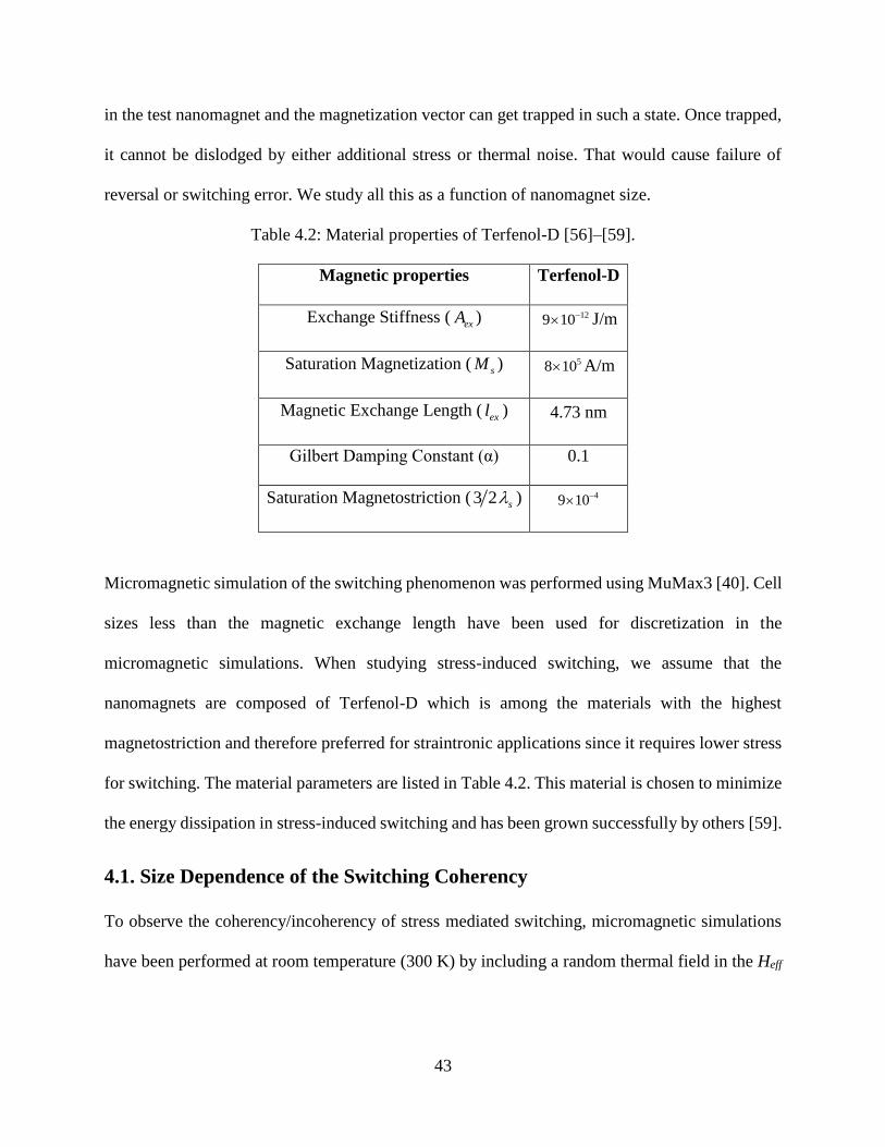
43
in the test nanomagnet and the magnetization vector can get trapped in such a state. Once trapped,
it cannot be dislodged by either additional stress or thermal noise. That would cause failure of
reversal or switching error. We study all this as a function of nanomagnet size.
Table 4.2: Material properties of Terfenol-D [56]–[59].
Magnetic properties Terfenol-D
Exchange Stiffness (exA ) 129 10 J/m
Saturation Magnetization (sM ) 58 10 A/m
Magnetic Exchange Length (exl ) 4.73 nm
Gilbert Damping Constant (α) 0.1
Saturation Magnetostriction (3 2 s ) 49 10
Micromagnetic simulation of the switching phenomenon was performed using MuMax3 [40]. Cell
sizes less than the magnetic exchange length have been used for discretization in the
micromagnetic simulations. When studying stress-induced switching, we assume that the
nanomagnets are composed of Terfenol-D which is among the materials with the highest
magnetostriction and therefore preferred for straintronic applications since it requires lower stress
for switching. The material parameters are listed in Table 4.2. This material is chosen to minimize
the energy dissipation in stress-induced switching and has been grown successfully by others [59].
4.1. Size Dependence of the Switching Coherency
To observe the coherency/incoherency of stress mediated switching, micromagnetic simulations
have been performed at room temperature (300 K) by including a random thermal field in the Heff
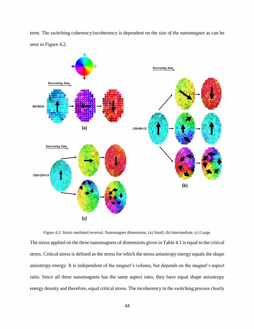
44
term. The switching coherency/incoherency is dependent on the size of the nanomagnet as can be
seen in Figure 4.2.
Figure 4.2: Strain mediated reversal. Nanomagnet dimensions, (a) Small, (b) Intermediate, (c) Large.
The stress applied on the three nanomagnets of dimensions given in Table 4.1 is equal to the critical
stress. Critical stress is defined as the stress for which the stress anisotropy energy equals the shape
anisotropy energy. It is independent of the magnet’s volume, but depends on the magnet’s aspect
ratio. Since all three nanomagnets has the same aspect ratio, they have equal shape anisotropy
energy density and therefore, equal critical stress. The incoherency in the switching process clearly
45
increases with increasing dimension. Exchange interaction forces the spins to rotate together in
unison in smaller nanomagnets resulting in a coherent rotation in the smallest nanomagnet as
shown in Figure 4.2.a. The magnetization rotates completely to the opposite direction after stress
withdrawal. Increasing the dimensions allows spins to reduce the exchange energy penalty be
amortizing over a larger number of spins, resulting in incoherent rotation in nanomagnets with
larger dimensions. Because of the incoherency in the switching process, two incoherent metastable
states, namely the C-state and vortex state are found in the larger nanomagnets when stress is
applied. The C-state is so named since in this state the spins seem to arrange themselves in the
form of the letter C (the spin texture curls to form the shape of the letter C). In the intermediate
sized nanomagnet, the possible outcomes after the application of stress as shown in Figure 4.2.b
are: (1) the magnetization can go through a nearly coherent rotation and emerge in the opposite
direction, thus completing the switching process, (2) the magnetization can go to the C-state until
the stress is withdrawn and come back to the initial state after stress withdrawal or (3) the
magnetization can enter the vortex state and remain there even after stress withdrawal. Among
these two incoherent metastable states, the C-state is the most prominent in the intermediate sized
nanomagnet while rarely entering the vortex state (< 1% probability). On the other hand, the C-
state is completely absent in the large nanomagnet. This magnet either switches successfully or
enters the vortex state and remains there as shown in Figure 4.3.c.
4.2. Switching Coherency Dependence of Dynamic Error
Switching error calculation has been performed at room temperature (300 K). The thermal field
causes erratic magnetization rotation and hence the magnetization may fail to rotate through 180o,
resulting in a switching error. The switching error has been estimated from simulations of 1000
switching trajectories (for each case). Stress is turned on at some time and we follow the temporal
46
evolution of the magnetization perturbed by a random thermal field (mimicking thermal noise) at
every simulation time step. This generates a switching trajectory in MuMax3 simulation. The
fraction of the trajectories that fail to switch by completing a ~180o rotation is the error probability.
We deliberately chose parameters where the switching error is 1% or higher, so that only 1000
micromagnetic simulations would suffice for generating the required statistics. To study switching
error probabilities < 1% we would need to increase the number of trajectories but we do not study
that regime as it is computationally prohibitive and more importantly the physics and trends
observed at errors rates over 1% would also scale to that regime. Hence, studying the low error
probability regime would have not only stretched our resources but also would have been
superfluous within the scope of this work.
Figure 3.3: Strain mediated switching. a) Stress profile in time domain. b) Dipole field strength vs. percentage of
switching error in stress mediated switching.
Figure 3.3.a shows the stress profile used in our simulations and was applied to all the
nanomagnets. The voltage required to generate the applied stress (~28 MPa) for a 100 nm thick
PZT thin film using the scheme shown in Fig. 1(b) is ~105 mV and the ferroelectric response can
be considered instantaneous. (The ferroelectric response has been demonstrated to have a

47
characteristic switching time constant of ~70-90 ps [60]). Figure 3.3[60]). Figure 15.b shows the
estimated switching error probability as a function of varying dipole coupling field. The results
show that the switching error probability decreases with increasing dipole field for all nanomagnet
dimensions. This is expected since the dipole field favors the +90o rotation (right) over the -90o
rotation (wrong) after stress removal and hence increasing its strength would reduce error
probability. However, the switching error probability also increases with increasing nanomagnet
size and this is due to increasing incoherency in the switching process which makes magnetization
dynamics increasingly vulnerable to thermal noise in larger nanomagnets.
There is another effect that is responsible for making larger nanomagnets more error-prone. In
larger nanomagnets, stress spawns metastable states (C-state and vortex state) in the nanomagnet’s
potential energy profile. They trap the magnetization and impede successful switching. Neither
additional stress, nor thermal noise, can easily dislodge the magnetization from the metastable
state. As shown in Figure 3.2, the metastable states can have a spin texture that is either C shaped
(present only in the intermediate dimension) or a vortex state (present in both intermediate and
large nanomagnets), both of which are highly incoherent states and therefore never present in the
small nanomagnet. This explains the high switching error in the intermediate and large
nanomagnets compared to the small one.
It should be noted that the C-state, once formed, is sustained in the presence of stress but it still
has net magnetization predominantly pointing in the initial direction. Hence, when stress is
withdrawn, it always returns the magnetization to the initial state, i.e. the nanomagnet does not
switch. The vortex state has a net magnetization equal to zero and has no memory of the initial
state. However, it too prevents switching because it is so stable that the magnetization remains in
this state even after stress is withdrawn. The difference is that that unlike the C-state, the vortex
48
state does not return the magnetization to the initial orientation upon stress withdrawal, but traps
it into a different orientation. The energy barrier that surrounds the metastable vortex state cannot
be overcome by the dipole coupling or thermal fluctuations at room temperature. Nor can stress
(even ~200 MPa) destroy this state, once formed. Thus, the only way intermediate and large
nanomagnets can reverse their magnetization successfully is by altogether avoiding the C- and
vortex-states. That is why the switching error probabilities are very high for intermediate and large
nanomagnets in Figure 3.3.b.
In the larger nanomagnet, the probability of formation of the vortex state decreases with increasing
dipole coupling that results in lower switching error as the dipole coupling is increased. This
reduced probability of formation of the vortex state is also true in intermediate nanomagnets but
the reduction in the probability of formation of the C-state is comparatively smaller in the range
of dipole fields studied. Thus, the decrease in switching error with increasing dipole coupling is
less pronounced in the intermediate sized nanomagnet compared to the large one as seen in Figure
3.3.b.
To verify that the observed trend in the switching error rates with respect to dipole field as shown
in Figure 3.3.b continues to the regime with error rates of <1%, we have simulated 10000
trajectories for the small (60nm - 40nm - 6nm) nanomagnet with dipole fields of 5.44mT and 7.23
mT under the same stress profile as shown in Fig. 3.3.a. The simulations show 5 and 2 errors
respectively out of the 10000 trajectories (0.05% and 0.02% error probability) whereas there were
5 errors out of 1000 trajectories for a dipole field of 3.3 mT (0.5%). So, the error rates are indeed
scaling.
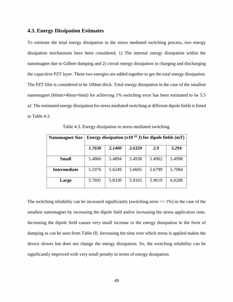
49
4.3. Energy Dissipation Estimates
To estimate the total energy dissipation in the stress mediated switching process, two energy
dissipation mechanisms have been considered, 1) The internal energy dissipation within the
nanomagnet due to Gilbert damping and 2) circuit energy dissipation in charging and discharging
the capacitive PZT layer. These two energies are added together to get the total energy dissipation.
The PZT film is considered to be 100nm thick. Total energy dissipation in the case of the smallest
nanomagnet (60nm×40nm×6nm) for achieving 1% switching error has been estimated to be 5.5
aJ. The estimated energy dissipation for stress mediated switching at different dipole fields is listed
in Table 4.3.
Table 4.3. Energy dissipation in stress mediated switching.
Nanomagnet Size
Energy dissipation (x10-18 J) for dipole fields (mT)
1.7630 2.1400 2.6320 2.9 3.294
Small 5.4860 5.4894 5.4938 5.4962 5.4998
Intermediate 5.5976 5.6249 5.6605 5.6799 5.7084
Large 5.7691 5.8330 5.9165 5.9619 6.0288
The switching reliability can be increased significantly (switching error << 1%) in the case of the
smallest nanomagnet by increasing the dipole field and/or increasing the stress application time.
Increasing the dipole field causes very small increase in the energy dissipation in the form of
damping as can be seen from Table III. Increasing the time over which stress is applied makes the
device slower but does not change the energy dissipation. So, the switching reliability can be
significantly improved with very small penalty in terms of energy dissipation.
50
4.4. Conclusion
This study shows that strain based switching is coherent in small nanomagnets (~60 nm × 40 nm
× 6 nm) and can be switched reliably. The switching gets more incoherent as the nanomagnets size
increases, leading to large errors in switching. All this indicates that straintronic switching is best
suited for small nanomagnets (lateral dimensions ~ 50 nm or smaller) that could result in reliable
switching and extremely energy efficient operation. However, there is one caveat. Normally, the
shape anisotropy barrier has to be sufficiently tall (~ 1.7 eV) to ensure enough thermal stability.
The stress anisotropy energy has to equal or exceed the barrier height in order to cause the 900
rotation that is necessary for the reversal. The stress anisotropy energy is the product of the stress,
the magnetostriction coefficient, and the nanomagnet volume. In smaller nanomagnets, we will
require either a larger stress (undesirable since it increases the switching voltage and energy
dissipation and in some cases it is impossible to apply as the strain that the piezoelectric can
generated is limited) or a larger magnetostriction coefficient. Terfenol-D with saturation
magnetostriction of ~1500 ppm [61] can be used in fabricating small nanomagnets. While this
material has indeed been sputtered to produce thin films with saturation magnetostriction of ~900
ppm [58], fabricating small nanomagnets with this material proves to be challenging. On the other
hand, materials like Co or Ni that have been used to demonstrate strain switched magnetostrictive
nanomagnets [7], [62] have saturation magnetostriction of only ~ 30 ppm. Using Ni/Co
nanomagnets, the stress anisotropy energy achievable at dimensions ~60 nm×40 nm×6 nm with a
stress as large as 100 MPa is a mere ~0.2 eV (~ 8kT at room temperature) which is way too low
to ensure sufficient thermal stability. There is a limit on the amount of stress that can be generated
or sustained. That precludes nanomagnets that are simultaneously small, amenable to switching by
stress and possess high stability against thermal noise at room temperature. Larger nanomagnets
51
would solve this issue as increasing the nanomagnet volume while retaining the same stress
anisotropy energy density allows the generation of larger stress anisotropy energy and hence a
larger shape anisotropy barrier for better thermal stability. Unfortunately, as this study shows,
larger nanomagnets are considerably more error-prone. This clearly demonstrates the challenges
that one faces in straintronics, namely the design of nanomagnets with sufficient thermal stability
and sufficient resilience against switching errors. A large magnetostriction is essential for scaling
while maintaining thermal stability and hence there is an urgent need to develop processes and
materials that yield high magnetostriction in nano-patterned structures.
This study has been published in IEEE Transactions on Electron Devices [63].
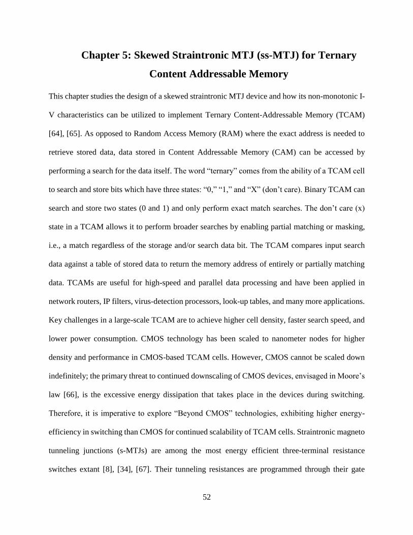
52
Chapter 5: Skewed Straintronic MTJ (ss-MTJ) for Ternary
Content Addressable Memory
This chapter studies the design of a skewed straintronic MTJ device and how its non-monotonic I-
V characteristics can be utilized to implement Ternary Content-Addressable Memory (TCAM)
[64], [65]. As opposed to Random Access Memory (RAM) where the exact address is needed to
retrieve stored data, data stored in Content Addressable Memory (CAM) can be accessed by
performing a search for the data itself. The word “ternary” comes from the ability of a TCAM cell
to search and store bits which have three states: “0,” “1,” and “X” (don’t care). Binary TCAM can
search and store two states (0 and 1) and only perform exact match searches. The don’t care (x)
state in a TCAM allows it to perform broader searches by enabling partial matching or masking,
i.e., a match regardless of the storage and/or search data bit. The TCAM compares input search
data against a table of stored data to return the memory address of entirely or partially matching
data. TCAMs are useful for high-speed and parallel data processing and have been applied in
network routers, IP filters, virus-detection processors, look-up tables, and many more applications.
Key challenges in a large-scale TCAM are to achieve higher cell density, faster search speed, and
lower power consumption. CMOS technology has been scaled to nanometer nodes for higher
density and performance in CMOS-based TCAM cells. However, CMOS cannot be scaled down
indefinitely; the primary threat to continued downscaling of CMOS devices, envisaged in Moore’s
law [66], is the excessive energy dissipation that takes place in the devices during switching.
Therefore, it is imperative to explore “Beyond CMOS” technologies, exhibiting higher energy-
efficiency in switching than CMOS for continued scalability of TCAM cells. Straintronic magneto
tunneling junctions (s-MTJs) are among the most energy efficient three-terminal resistance
switches extant [8], [34], [67]. Their tunneling resistances are programmed through their gate
53
potentials, which induce strain in the magnetostrictive free-layer of the device leading to
magnetization switching that changes the tunneling current at a given voltage. Unfortunately, s-
MTJs are also relatively error-prone [9], [43], [45], [47], [63] and have low resistance ON/OFF
ratios. The best case switching error probability, even theoretically is typically larger than 10−9 at
room temperature, which makes it problematic to utilize them in Boolean logic. This has turned
attention to non-Boolean computing paradigms [4], [5], [68]–[70], such as those employing
TCAM, which may be more forgiving of errors and do not always demand high-resistance
ON/OFF ratios. ss-MTJs will be ideal for such applications. In order to implement a high
performance TCAM cell, a novel adaptation of s-MTJ is presented, henceforth mentioned as a
skewed s-MTJ or an ss-MTJ, where the MTJ resistance can be controlled by two gate-terminals.
The resistance through a skewed s-MTJ is maximum when the potentials at the first and second
gate terminals (i.e., V2 and V3, respectively) follow V3 = V2 + VF, where VF is a fixed voltage that
we call the “offset voltage.” Resistance in a skewed s-MTJ drops steeply when V2 and V3 deviate
from the above “match” condition. Therefore, the current through a skewed s-MTJ characterizes
similarity between the potentials at the two gate terminals, V2 and V3. This unique characteristic
of the skewed s-MTJ is exploited to design one transistor, one trench capacitor, and a single ss-
MTJ-based dynamic TCAM cell. It is shown that the low ON/OFF ratio in skewed s-MTJ does not
inhibit circuit operation, although a higher ON/OFF ratio would be desirable.
5.1. Skewed Straintronic Magneto Tunneling Junction
Similar to a standard MTJ, an s-MTJ also comprises a stack of fixed layer-spacer-free layer.
However, unlike current based switching in MTJ, an s-MTJ switches by the action of gate-induced
strain in the free-layer. The free layer in s-MTJ is a magnetostrictive nanomagnet in elastic contact
with an underlying poled piezoelectric thin film of thickness a, as shown in Fig. 5.1(a). Square

54
electrodes of edge L (≈ a), separated by a distance d (L ≤ d ≤ 2L), are delineated on the piezoelectric
surrounding the MTJ stack. The bottom of the conducting substrate is grounded. Electrode “1” is
used to read the s-MTJ resistance by passing a current to ground.
Figure 5.1: (a) Four-terminal skewed s-MTJ switch showing the MTJ stack, the piezoelectric layer, and the electrodes.
(b) Top view of the free and fixed layers of the MTJ. The major axes of the two ellipses subtend an angle of 45°
between themselves.
Application of a voltage across the piezoelectric film using the shorted electrode pair “2” shown
in Fig. 5.1.a generates biaxial strain in the film (compression along the line joining the electrode
pair and tension perpendicular to it, or vice versa, depending on the polarity of the voltage), which
is partially or fully transferred to the soft layer of the s-MTJ in elastic contact with the film. This
rotates its magnetization through the Villari effect and changes the s-MTJ resistance, realizing the
action of a switch. A tiny amount of voltage V (few mV) is required to rotate the magnetization
through a large angle and change the s-MTJ resistance substantially if the piezoelectric film is
∼100-nm thick, resulting in a switching energy dissipation CV2 (C is the capacitance associated
with charging the piezoelectric, which is 1–2 fF) of a few tens of aJ [7], [71]. The internal energy
dissipation within the magnetostrictive free layer due to Gilbert damping is negligible [67] as is
55
the mechanical energy dissipation due to strain. The s-MTJ operation has been experimentally
demonstrated [72], [73].
Here, we show that an s-MTJ can be engineered to produce very unusual device characteristics.
This characteristics are then utilized by our collaborators at UIC to implement TCAM behavior
which will also be briefly discussed. Consider a “skewed” s-MTJ where the major axes of the fixed
and free layers subtend an angle of 45° between them, as shown in Fig. 5.1.b. The fixed layer is
implemented with a synthetic antiferromagnet to reduce the dipole interaction with the free layer,
but not completely eliminate it. Because of shape anisotropy, the magnetization orientations of
both layers will lie along the respective major axes of the ellipses, but owing to the remnant dipole
interaction, the angle between them will be obtuse rather than acute (see Fig. 5.1.b). In all
simulations we assume the magnetization of the free layer initially makes an obtuse angle with the
magnetization of the fixed layer. When the free layer is strained by the voltage applied to the
electrode pairs “2,” its magnetization begins to rotate. The remnant dipole interaction will make it
rotate clockwise in Fig. 5.1.b so as to always increase the angular separation between the
magnetizations of the two layers. We have simulated the magnetization rotation under strain in the
presence of thermal noise using stochastic Landau– Lifshitz–Gilbert (s-LLG) simulations (see later
description). Out of 107 switching trajectories simulated, not a single one rotated anticlockwise,
showing that the clockwise rotation is overwhelmingly preferred. This also indicates that the
magnetization dynamics is robust and reliable with error probability < 10-7.
Initially, before the application of strain, the magnetizations of the fixed and free layers subtend
an angle θ = 135°, as shown in Fig. 5.1.b. Upon application of strain, the magnetization begins to
rotate clockwise and θ gradually increases from 135° to 225°. The MTJ resistance depends on θ
according to [74]
56
( ) 1 cos( )
(1 cos( )) 2
P
AP P
R R
R R
(5.1)
where ( )P APR is the MTJ resistance when the magnetizations of the fixed and free layers are parallel
(antiparallel), ( )R is the resistance when the angular separation between the magnetizations is
, and ( ) /AP P PR R R . Since varies between 135° and 225°, the conductance of the MTJ (or
current flowing through terminal “1” at a fixed bias) plotted as a function of the voltage applied to
the terminal “2” (which generates the rotation) will exhibit a “valley.” The bottom of the valley
corresponds to 180 when the MTJ resistance becomes maximum.
We can alter the stress distribution in the free layer of the s-MTJ by applying an additional voltage
across the piezoelectric with the third pair of electrodes “3” shown in Fig. 5.1.a. This will allow
us to shift the position of the valley bottom in the transconductance characteristic I1 versus V2 (In
is the current through the nth terminal at a fixed bias and Vn is the voltage applied to the nth
terminal). Thus, we have a 4-terminal switch with terminals “1,” “2,” “3,” and ground, where the
current between “1” and ground is changed with the voltage applied to “2” and the transfer
characteristic associated with this change can be modulated by a voltage applied to the terminal
“3.” When both electrode pairs “2” and “3” are activated, the strain distribution in the piezoelectric
(and hence in the free layer of the s-MTJ) becomes complex. Exact strain profiles can be calculated
with 3-D finite-element analysis (e.g., with COMSOL Multiphysics package) as in [73], [75];
however, to keep the analysis tractable, we will assume that activating an electrode pair generates
only uniaxial stress along the line joining that pair. Note that if anything, this overestimates the
stress required to produce a given rotation θ, and is hence conservative. The sign of the uniaxial
stress (tensile or compressive) depends on the polarity of the voltage. If we activate electrode pair
“2,” then we will generate uniaxial stress along the major axis of the elliptical free layer of the s-

57
MTJ (compressive or tensile depending on the voltage polarity at “2”), whereas if we activate
electrode pair “3,” we will generate uniaxial stress along the minor axis of the free layer. We have
assumed that the free layer is made of Terfenol-D, which has a positive and large magnetostriction
coefficient (600 ppm). Compressive stress along any direction in the free layer will rotate its
magnetization away from that direction (maximum rotation is 90°), while tensile stress will keep
it aligned along that direction. This allows us to control the angle θ with voltages at “2” and “3.”
We have computed θ versus the voltage V2 (assuming V3 = 0) at 0 K temperature (no thermal
noise) using the Landau–Lifshitz–Gilbert equation, which yields the magnetization orientation of
the free layer as a function of time t under the influence of voltage generated stress
( )
( ) ( ) ( ) ( ) ( )eff eff
s
dM tM t H t M t M t H t
Mdt
(5.2)
where sM is the saturation magnetization of the free layer material, is the gyromagnetic ratio,
is the Gilbert damping constant in the free layer, and ( )effH t is the effective magnetic field
experienced by the free layer at any time t and is given by
( ) ( ) ( ) ( )eff dipole shape stress thermalH t H H t H t H t (5.3)
where dipoleH is the (constant) dipole field exerted by the fixed layer, ( )shapeH t is the field due to
shape anisotropy, ( )stressH t is the field generated by stress, and ( )thermalH t is the random field due
to thermal noise, which has been discussed in chapter 1. Stress is generated in the piezoelectric
substrate by activating a shorted electrode pair with a voltage V. The resulting stress is assumed
to be uniaxial along the line joining the centers of the electrodes in the activated pair. The voltage
V generates a vertical electric field of V/a in the piezoelectric substrate. Following [18], we will
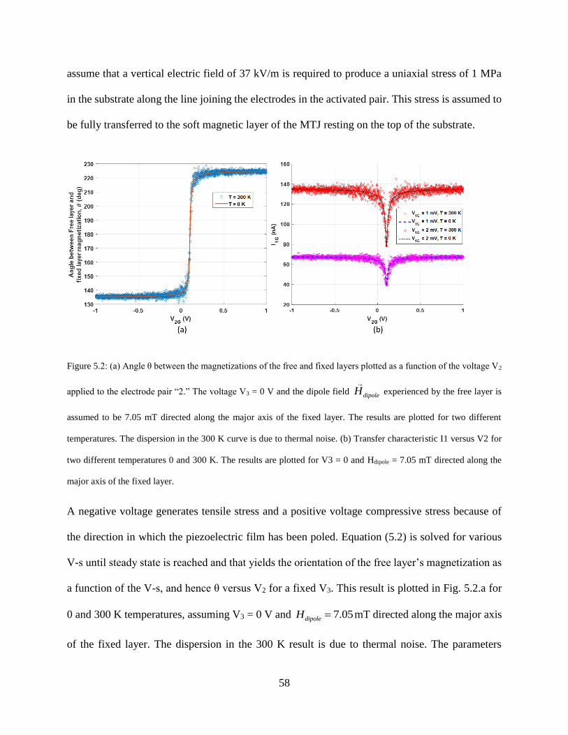
58
assume that a vertical electric field of 37 kV/m is required to produce a uniaxial stress of 1 MPa
in the substrate along the line joining the electrodes in the activated pair. This stress is assumed to
be fully transferred to the soft magnetic layer of the MTJ resting on the top of the substrate.
Figure 5.2: (a) Angle θ between the magnetizations of the free and fixed layers plotted as a function of the voltage V2
applied to the electrode pair “2.” The voltage V3 = 0 V and the dipole field dipoleH experienced by the free layer is
assumed to be 7.05 mT directed along the major axis of the fixed layer. The results are plotted for two different
temperatures. The dispersion in the 300 K curve is due to thermal noise. (b) Transfer characteristic I1 versus V2 for
two different temperatures 0 and 300 K. The results are plotted for V3 = 0 and Hdipole = 7.05 mT directed along the
major axis of the fixed layer.
A negative voltage generates tensile stress and a positive voltage compressive stress because of
the direction in which the piezoelectric film has been poled. Equation (5.2) is solved for various
V-s until steady state is reached and that yields the orientation of the free layer’s magnetization as
a function of the V-s, and hence θ versus V2 for a fixed V3. This result is plotted in Fig. 5.2.a for
0 and 300 K temperatures, assuming V3 = 0 V and 7.05dipoleH mT directed along the major axis
of the fixed layer. The dispersion in the 300 K result is due to thermal noise. The parameters
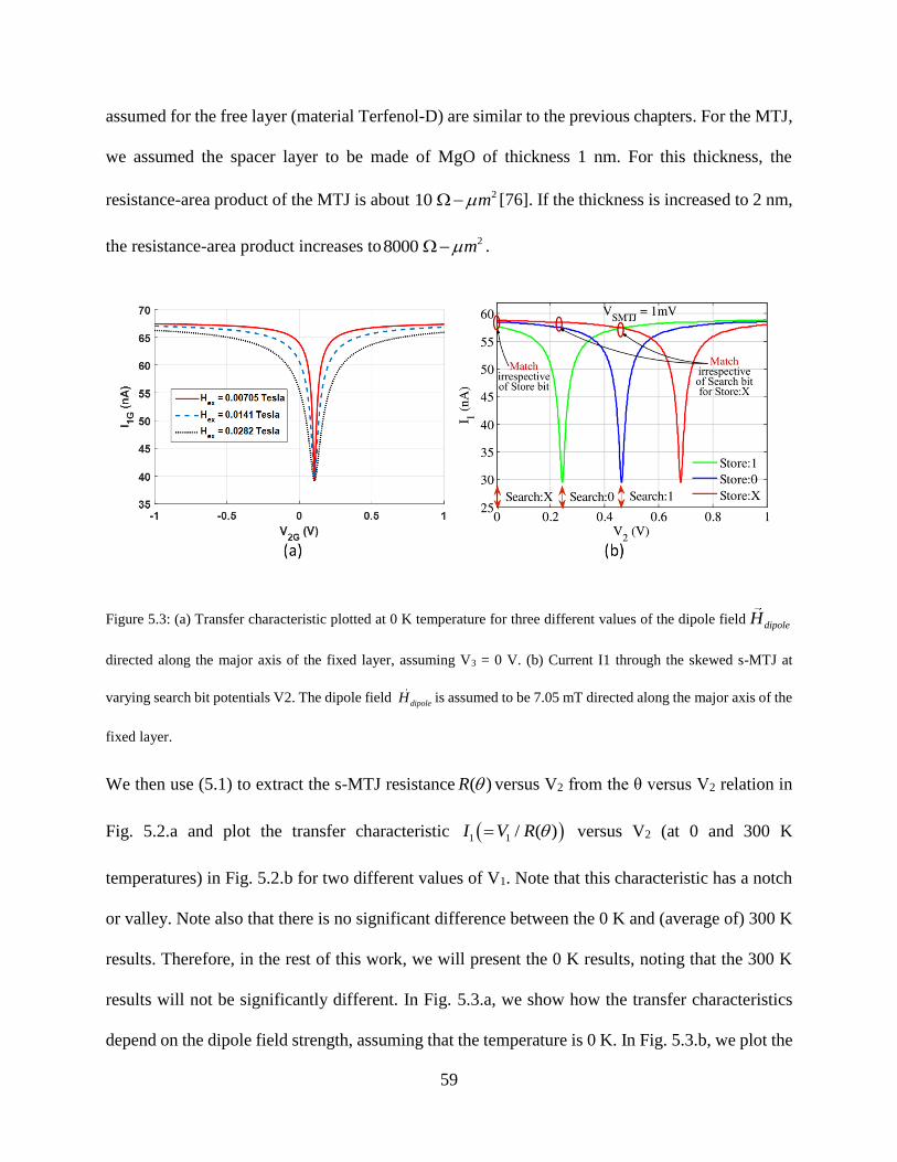
59
assumed for the free layer (material Terfenol-D) are similar to the previous chapters. For the MTJ,
we assumed the spacer layer to be made of MgO of thickness 1 nm. For this thickness, the
resistance-area product of the MTJ is about 210 m [76]. If the thickness is increased to 2 nm,
the resistance-area product increases to 28000 m .
Figure 5.3: (a) Transfer characteristic plotted at 0 K temperature for three different values of the dipole field dipoleH
directed along the major axis of the fixed layer, assuming V3 = 0 V. (b) Current I1 through the skewed s-MTJ at
varying search bit potentials V2. The dipole field dipoleH is assumed to be 7.05 mT directed along the major axis of the
fixed layer.
We then use (5.1) to extract the s-MTJ resistance ( )R versus V2 from the θ versus V2 relation in
Fig. 5.2.a and plot the transfer characteristic 1 1 / ( )I V R versus V2 (at 0 and 300 K
temperatures) in Fig. 5.2.b for two different values of V1. Note that this characteristic has a notch
or valley. Note also that there is no significant difference between the 0 K and (average of) 300 K
results. Therefore, in the rest of this work, we will present the 0 K results, noting that the 300 K
results will not be significantly different. In Fig. 5.3.a, we show how the transfer characteristics
depend on the dipole field strength, assuming that the temperature is 0 K. In Fig. 5.3.b, we plot the
60
transfer characteristic I1 versus V2 at 0 K temperature for three different values of V3. Clearly, the
position of the notch can be shifted around with the voltage V3, which generates an additional
uniaxial stress (negative voltage tensile and positive voltage compressive) along the line joining
the electrode pads “3.” This makes it a 4-terminal switch.
Table 5.1: Voltage levels used to encode store and search bits.
Store Bit Search Bit
Bit Value Voltage Level (V) Bit Value Voltage Level (V)
1 0.24 X 0
0 0.46 0 0.24
X 0.68 1 0.46
The unique characteristic of a skewed s-MTJ can significantly simplify the design and operation
of a TCAM cell. In a skewed s-MTJ, the MTJ resistance can be controlled by the gate voltages V2
and V3. The resistance of a skewed s-MTJ becomes maximum when V2 and V3 “match,” i.e., they
differ only by a fixed amount, which we have called the “offset.” This associative property of the
skewed s-MTJ has enabled the design of a one transistor, one trench capacitor, and a single ss-
MTJ-based dynamic TCAM cell. A CMOS-based static TCAM cell requires 16 transistors for each
cell [77]. Likewise, a CMOS-based dynamic TCAM cell requires six transistors and two trench
capacitors for each cell [78]. Power dissipation in CMOS-based TCAM cells is high due to a large
number of transistors resulting in more parasitic nodes.
Fig. 5.3.b and table 5.1 shows the encoding scheme for implementing the match operation of a
TCAM cell through a single skewed s-MTJ. In Fig. 5.3.b, the ss-MTJ current (I1) is shown at
varying search bit potentials (i.e., V2 potential) and at varying stored bits (i.e., V3 potential). The

61
search bits “X,” “0,” and “1” are encoded as 0, 0.24, and 0.46 V, respectively. The store bits “1,”
“0,” and “X” center the ss-MTJ valley to 0.24, 0.46, and 0.68 V, respectively. In the encoding
scheme, a high ss-MTJ current (i.e., a lower resistance in the ss-MTJ) indicates a match between
the stored and the search bit. The I1–V2 valley in the ss-MTJ is programmed to the farthest right
for the don’t care state (i.e., “X”) storage, as shown in Fig. 5.3.b. Therefore, the ss-MTJ current is
high for all search bits (“0,” “1,” and “X”) denoting a match irrespective of the applied search bit.
The search bit “X” is encoded as 0 V. Hence, at search bit “X,” the ss-MTJ current is high for all
stored states (“0,” “1,” and “X”), denoting a match irrespective of the stored bit. Therefore, the
skewed s-MTJ significantly reduces the complexity of match operation in a TCAM.
5.2. TCAM Implementation
Figure 5.4: ss-MTJ-based dynamic TCAM cell.
In a skewed s-MTJ (ss-MTJ), the current I1 between the free and fixed layers can be controlled by
the gate voltages at V2 and V3 (see Fig. 5.3b). At any given value of V1, I1 is lowest when V3 = V2
+ VF, where VF is a fixed voltage (offset voltage). The current I1 increases steeply when V2 and
V3 deviate from the “match” condition. In this section, we discuss an area/energy-efficient TCAM
cell, exploiting this associative processing capability of skewed s-MTJ. The cell schematic for an
ss-MTJ-based dynamic TCAM is shown in Fig. 5.4. The cell exploits high parasitic capacitance at
62
V3 node for a dynamic storage of the storage bit. Note that the capacitance at V3 is high due to an
underlying high dielectric constant ( 1000 ) piezoelectric layer. The parasitic capacitance can
be further enhanced by thinning down the piezoelectric layer, and/or by increasing the contact area
of V3 electrode atop the piezoelectric layer. In addition to V3 node capacitance, a trench
capacitance can be used for a stable storage. A net 30 fF capacitance is assumed here at the V3
node. The capacitor is charged through the access transistor M1. However, due to charge leakage,
refreshing of the stored potential at the capacitor (C) is necessary, which can be achieved by the
refresh voltage VR. The detailed implementation of the ss-MTJ based TCAM cell circuitry and
characteristics can be found in References [64], [65].
5.3. Comparison between ss-MTJ and CMOS based TCAM
The TCAM cell implemented with the ss-MTJ device discussed here with further details in [64],
[65], the operation is non-Boolean and single-ended, which minimizes dynamic power and routing.
The power-performance analysis of a TCAM array based on ss-MTJ-TCAM cells shows that the
proposed design possesses the potential to implement high-density, high-speed, and energy-
efficient large-scale TCAM systems. Exploiting the non-monotonic I-V characteristics of the
proposed ss-MTJ device allows designing a dynamic TCAM cell with only one transistor, one
trench capacitor, and a single ss-MTJ compared to a CMOS-based static static TCAM cell which
requires 16 transistors for each cell [77] and dynamic TCAM cell which requires six transistors
and two trench capacitors for each cell [78]. This significantly reduces the total area requirement
for the TCAM. Compared with CMOS-based TCAM, the ss-MTJ-based design shows ∼10.8×
lower minimum Energy Delay Product (EDP). Moreover, the frequency at minimum EDP in the
discussed ss-MTJ-TCAM is ∼9.4× higher than the frequency of minimum EDP in CMOS-based

63
TCAM. At an operational frequency of ∼1 GHz, the extrapolated EDP of CMOS-TCAM is ∼100×
larger than that of ss-MTJ-based TCAM.
5.4. Conclusion
The proposed ss-MTJ-TCAM also outperforms other state-ofthe-art MTJ-based-TCAM designs
in terms of cell density, search delay, and search energy. Therefore, the ss-MTJ-based TCAM can
meet the stringent density and performance requirements in the emerging computing platforms
such as for routers in IoT. This shows that one of the key potential applications of straintronic
devices in the future is in non-volatile computing.
This study was performed in collaboration with Prof. Amit Trivedi and his graduate student Ms.
Susmita Manasi who performed the TCAM implementation and associated circuit level design and
analysis at University of Illinois at Chicago. The ss-MTJ device modeling and simulation was
performed by Md Mamun Al-Rashid with inputs from Prof. J. Atulasimha and Prof. S.
Bandyopadhyay) at Virginia Commonwealth University, Richmond, Virginia. This work has been
published as two part paper in IEEE Trans. on Electron Devices [64], [65].
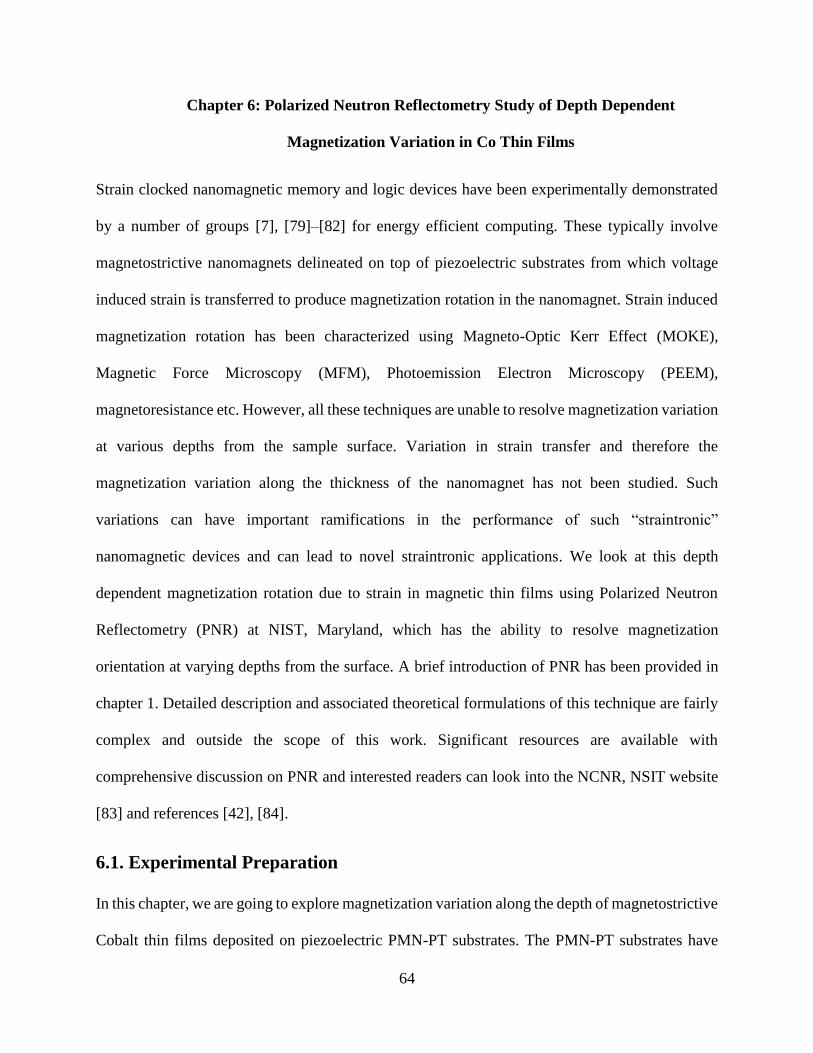
64
Chapter 6: Polarized Neutron Reflectometry Study of Depth Dependent
Magnetization Variation in Co Thin Films
Strain clocked nanomagnetic memory and logic devices have been experimentally demonstrated
by a number of groups [7], [79]–[82] for energy efficient computing. These typically involve
magnetostrictive nanomagnets delineated on top of piezoelectric substrates from which voltage
induced strain is transferred to produce magnetization rotation in the nanomagnet. Strain induced
magnetization rotation has been characterized using Magneto-Optic Kerr Effect (MOKE),
Magnetic Force Microscopy (MFM), Photoemission Electron Microscopy (PEEM),
magnetoresistance etc. However, all these techniques are unable to resolve magnetization variation
at various depths from the sample surface. Variation in strain transfer and therefore the
magnetization variation along the thickness of the nanomagnet has not been studied. Such
variations can have important ramifications in the performance of such “straintronic”
nanomagnetic devices and can lead to novel straintronic applications. We look at this depth
dependent magnetization rotation due to strain in magnetic thin films using Polarized Neutron
Reflectometry (PNR) at NIST, Maryland, which has the ability to resolve magnetization
orientation at varying depths from the surface. A brief introduction of PNR has been provided in
chapter 1. Detailed description and associated theoretical formulations of this technique are fairly
complex and outside the scope of this work. Significant resources are available with
comprehensive discussion on PNR and interested readers can look into the NCNR, NSIT website
[83] and references [42], [84].
6.1. Experimental Preparation
In this chapter, we are going to explore magnetization variation along the depth of magnetostrictive
Cobalt thin films deposited on piezoelectric PMN-PT substrates. The PMN-PT substrates have
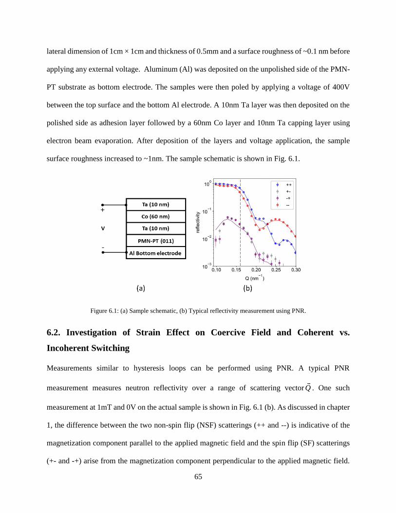
65
lateral dimension of 1cm × 1cm and thickness of 0.5mm and a surface roughness of ~0.1 nm before
applying any external voltage. Aluminum (Al) was deposited on the unpolished side of the PMN-
PT substrate as bottom electrode. The samples were then poled by applying a voltage of 400V
between the top surface and the bottom Al electrode. A 10nm Ta layer was then deposited on the
polished side as adhesion layer followed by a 60nm Co layer and 10nm Ta capping layer using
electron beam evaporation. After deposition of the layers and voltage application, the sample
surface roughness increased to ~1nm. The sample schematic is shown in Fig. 6.1.
Figure 6.1: (a) Sample schematic, (b) Typical reflectivity measurement using PNR.
6.2. Investigation of Strain Effect on Coercive Field and Coherent vs.
Incoherent Switching
Measurements similar to hysteresis loops can be performed using PNR. A typical PNR
measurement measures neutron reflectivity over a range of scattering vector Q . One such
measurement at 1mT and 0V on the actual sample is shown in Fig. 6.1 (b). As discussed in chapter
1, the difference between the two non-spin flip (NSF) scatterings (++ and --) is indicative of the
magnetization component parallel to the applied magnetic field and the spin flip (SF) scatterings
(+- and -+) arise from the magnetization component perpendicular to the applied magnetic field.
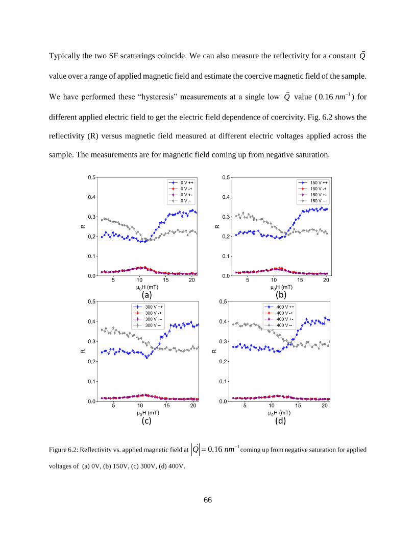
66
Typically the two SF scatterings coincide. We can also measure the reflectivity for a constant Q
value over a range of applied magnetic field and estimate the coercive magnetic field of the sample.
We have performed these “hysteresis” measurements at a single low Q value ( 10.16 nm ) for
different applied electric field to get the electric field dependence of coercivity. Fig. 6.2 shows the
reflectivity (R) versus magnetic field measured at different electric voltages applied across the
sample. The measurements are for magnetic field coming up from negative saturation.
Figure 6.2: Reflectivity vs. applied magnetic field at 10.16 Q nm coming up from negative saturation for applied
voltages of (a) 0V, (b) 150V, (c) 300V, (d) 400V.
67
The crossover points between the two non-spin flip scatterings in Fig. 6.2 indicate that the
magnetization component parallel to the applied field is zero at those points. The peaks in spin flip
scatterings indicate the maxima of perpendicular magnetization components.
Figure 6.3: (a) Spin asymmetry vs. magnetic field and (b) spin flip scattering vs. magnetic field at different applied
voltages.
Fig. 6.3 shows a replotted version of the data shown in Fig. 6.2 which makes visualizing the voltage
induced effects easier. Fig. 6.3(a) shows spin asymmetry R R R R vs. the applied
magnetic field. Change of sign in spin asymmetry indicates switching in the parallel magnetization
component. The field where spin asymmetry is zero can be defined as the coercive magnetic field
0H . Both Fig. 6.3(a) and 6.3(b) shows a rightward shift in the magnetic field where the spin
asymmetry becomes zero and the peaks of the SF scattering reflectivities respectively with
increasing electric voltage. These observations suggest that the stress anisotropy for a positive
applied voltage induces a magnetization “easy axis” (energetically favorable direction) along the
applied magnetic field and therefore, increasing the coercive magnetic field of the sample. Fig.
6.3(a) shows a 1.57 mT increase in 0H when the applied voltage goes from 0 to 400V. Fig. 6.3(b)
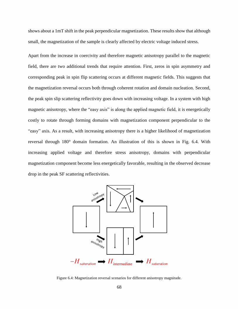
68
shows about a 1mT shift in the peak perpendicular magnetization. These results show that although
small, the magnetization of the sample is clearly affected by electric voltage induced stress.
Apart from the increase in coercivity and therefore magnetic anisotropy parallel to the magnetic
field, there are two additional trends that require attention. First, zeros in spin asymmetry and
corresponding peak in spin flip scattering occurs at different magnetic fields. This suggests that
the magnetization reversal occurs both through coherent rotation and domain nucleation. Second,
the peak spin slip scattering reflectivity goes down with increasing voltage. In a system with high
magnetic anisotropy, where the “easy axis” is along the applied magnetic field, it is energetically
costly to rotate through forming domains with magnetization component perpendicular to the
“easy” axis. As a result, with increasing anisotropy there is a higher likelihood of magnetization
reversal through 180° domain formation. An illustration of this is shown in Fig. 6.4. With
increasing applied voltage and therefore stress anisotropy, domains with perpendicular
magnetization component become less energetically favorable, resulting in the observed decrease
drop in the peak SF scattering reflectivities.
Figure 6.4: Magnetization reversal scenarios for different anisotropy magnitude.
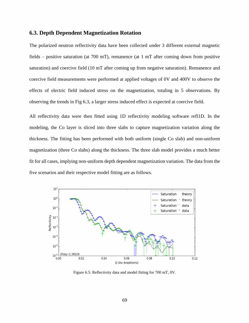
69
6.3. Depth Dependent Magnetization Rotation
The polarized neutron reflectivity data have been collected under 3 different external magnetic
fields – positive saturation (at 700 mT), remanence (at 1 mT after coming down from positive
saturation) and coercive field (10 mT after coming up from negative saturation). Remanence and
coercive field measurements were performed at applied voltages of 0V and 400V to observe the
effects of electric field induced stress on the magnetization, totaling in 5 observations. By
observing the trends in Fig 6.3, a larger stress induced effect is expected at coercive field.
All reflectivity data were then fitted using 1D reflectivity modeling software refl1D. In the
modeling, the Co layer is sliced into three slabs to capture magnetization variation along the
thickness. The fitting has been performed with both uniform (single Co slab) and non-uniform
magnetization (three Co slabs) along the thickness. The three slab model provides a much better
fit for all cases, implying non-uniform depth dependent magnetization variation. The data from the
five scenarios and their respective model fitting are as follows.
Figure 6.5: Reflectivity data and model fitting for 700 mT, 0V.
70
1. Positive saturation (700 mT external magnetic field and 0V)
The 700 mT field is enough to saturate the Co and we can consider the magnetization to completely
point along the applied magnetic field. While fitting this data set, the magnetization is therefore
assumed to be uniform and pointing towards the applied magnetic field direction (270°). Only the
structural parameters were allowed to change during the fitting. The reflectivity data and the
corresponding model fitting using refl1D are shown in Fig. 6.5.
The various parameters extracted after fitting are summarized in table 6.1.
Table: 6.1: Fitted model parameters in saturation.
Layer Thickness (Å) SLD (10-6/Å2)
Ta seed 132.9 3.714
Co 575.4 2.265
Ta capping 114.8 3.764
2. Remanence (1 mT external magnetic field at 0V and 400V)
The magnetic field is reduced from 700 mT to 1mT and the remanence magnetization is observed.
The structural parameters remains the same as the saturation case. The parameters that was allowed
to change during this fitting are the magnetizations of the three Co layer and their corresponding
magnetic scattering length density. In the case of 400V applied voltage, a biaxial strain is generated
in the PMN-PT substrate which is then transferred onto the Co layer. As already discussed, the
nature of the strain is such that it facilitates magnetization orientation along the applied magnetic
field. The reflectivity data and the corresponding fit are shown in Fig. 6.6. Please note that, the
magnetization rotation is not purely coherent. As a result, the modeled magnetization orientations
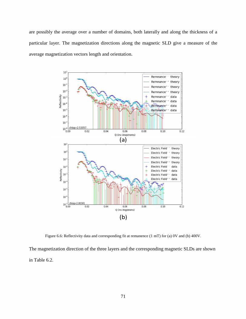
71
are possibly the average over a number of domains, both laterally and along the thickness of a
particular layer. The magnetization directions along the magnetic SLD give a measure of the
average magnetization vectors length and orientation.
Figure 6.6: Reflectivity data and corresponding fit at remanence (1 mT) for (a) 0V and (b) 400V.
The magnetization direction of the three layers and the corresponding magnetic SLDs are shown
in Table 6.2.
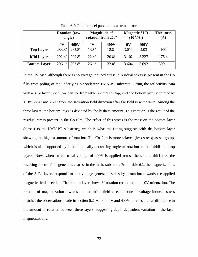
72
Table 6.2: Fitted model parameters at remanence.
Rotation (raw
angle)
Magnitude of
rotation from 270º
Magnetic SLD
(10-6/Å2)
Thickness
(Å)
0V 400V 0V 400V 0V 400V
Top Layer 283.8º 282.8º 13.8º 12.8º 3.013 3.03 100
Mid Layer 292.4º 290.8º 22.4º 20.8º 3.102 3.227 175.4
Bottom Layer 296.1º 292.8º 26.1º 22.8º 3.604 3.692 300
In the 0V case, although there is no voltage induced stress, a residual stress is present in the Co
film from poling of the underlying piezoelectric PMN-PT substrate. Fitting the reflectivity data
with a 3 Co layer model, we can see from table 6.2 that the top, mid and bottom layer is rotated by
13.8°, 22.4° and 26.1° from the saturation field direction after the field is withdrawn. Among the
three layers, the bottom layer is deviated by the highest amount. This rotation is the result of the
residual stress present in the Co film. The effect of this stress is the most on the bottom layer
(closest to the PMN-PT substrate), which is what the fitting suggests with the bottom layer
showing the highest amount of rotation. The Co film is more relaxed (less stress) as we go up,
which is also supported by a monotonically decreasing angle of rotation in the middle and top
layers. Now, when an electrical voltage of 400V is applied across the sample thickness, the
resulting electric field generates a stress in the in the substrate. From table 6.2, the magnetizations
of the 3 Co layers responds to this voltage generated stress by a rotation towards the applied
magnetic field direction. The bottom layer shows 3° rotation compared to its 0V orientation. The
rotation of magnetization towards the saturation field direction due to voltage induced stress
matches the observations made in section 6.2. At both 0V and 400V, there is a clear difference in
the amount of rotation between three layers, suggesting depth dependent variation in the layer
magnetizations.
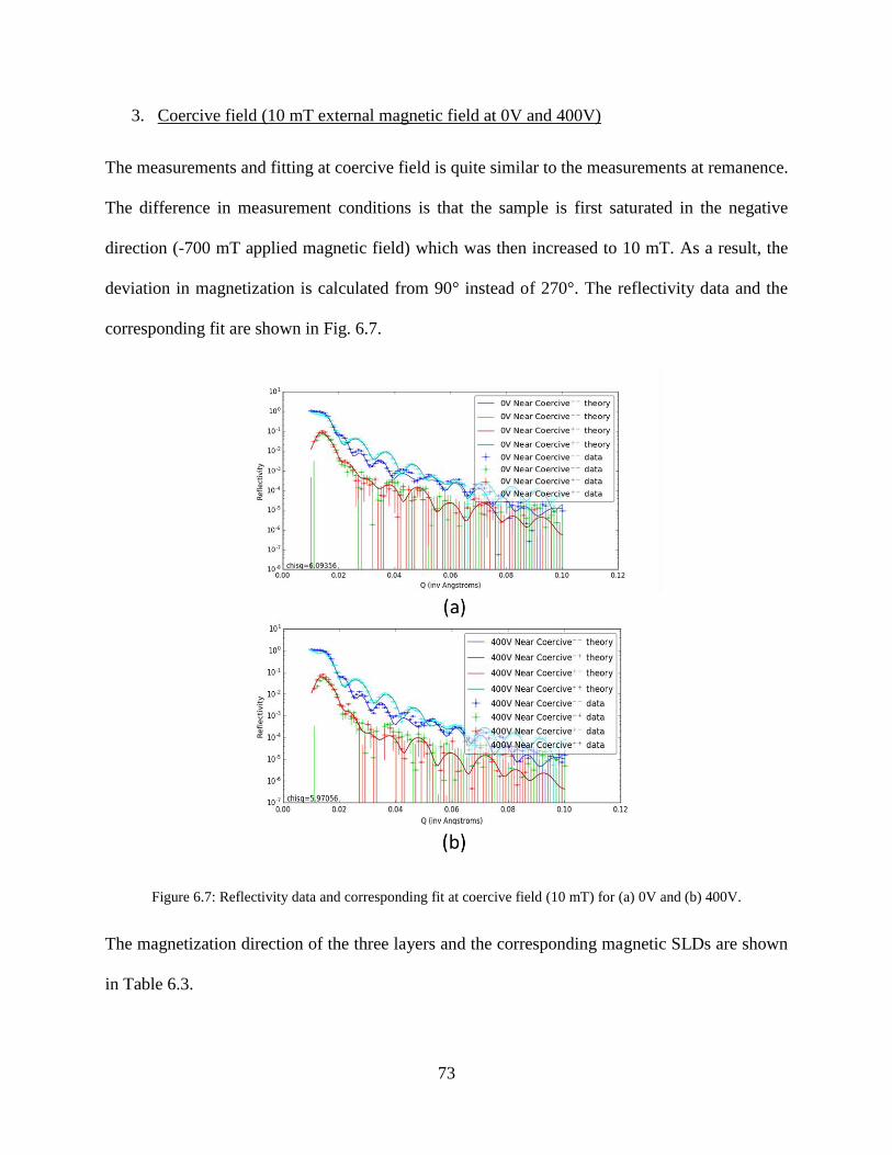
73
3. Coercive field (10 mT external magnetic field at 0V and 400V)
The measurements and fitting at coercive field is quite similar to the measurements at remanence.
The difference in measurement conditions is that the sample is first saturated in the negative
direction (-700 mT applied magnetic field) which was then increased to 10 mT. As a result, the
deviation in magnetization is calculated from 90° instead of 270°. The reflectivity data and the
corresponding fit are shown in Fig. 6.7.
Figure 6.7: Reflectivity data and corresponding fit at coercive field (10 mT) for (a) 0V and (b) 400V.
The magnetization direction of the three layers and the corresponding magnetic SLDs are shown
in Table 6.3.
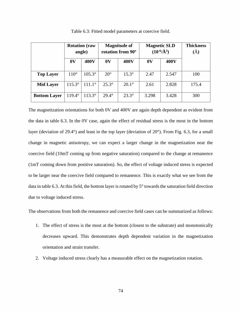
74
Table 6.3: Fitted model parameters at coercive field.
Rotation (raw
angle)
Magnitude of
rotation from 90º
Magnetic SLD
(10-6/Å2)
Thickness
(Å)
0V 400V 0V 400V 0V 400V
Top Layer 110° 105.3° 20° 15.3° 2.47 2.547 100
Mid Layer 115.3° 111.1° 25.3° 20.1° 2.61 2.828 175.4
Bottom Layer 119.4° 113.3° 29.4° 23.3° 3.298 3.428 300
The magnetization orientations for both 0V and 400V are again depth dependent as evident from
the data in table 6.3. In the 0V case, again the effect of residual stress is the most in the bottom
layer (deviation of 29.4°) and least in the top layer (deviation of 20°). From Fig. 6.3, for a small
change in magnetic anisotropy, we can expect a larger change in the magnetization near the
coercive field (10mT coming up from negative saturation) compared to the change at remanence
(1mT coming down from positive saturation). So, the effect of voltage induced stress is expected
to be larger near the coercive field compared to remanence. This is exactly what we see from the
data in table 6.3. At this field, the bottom layer is rotated by 5° towards the saturation field direction
due to voltage induced stress.
The observations from both the remanence and coercive field cases can be summarized as follows:
1. The effect of stress is the most at the bottom (closest to the substrate) and monotonically
decreases upward. This demonstrates depth dependent variation in the magnetization
orientation and strain transfer.
2. Voltage induced stress clearly has a measurable effect on the magnetization rotation.
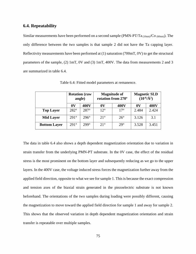
75
6.4. Repeatability
Similar measurements have been performed on a second sample (PMN-PT/Ta (10nm)/Co (60nm)). The
only difference between the two samples is that sample 2 did not have the Ta capping layer.
Reflectivity measurements have been performed at (1) saturation (700mT, 0V) to get the structural
parameters of the sample, (2) 1mT, 0V and (3) 1mT, 400V. The data from measurements 2 and 3
are summarized in table 6.4.
Table 6.4: Fitted model parameters at remanence.
Rotation (raw
angle)
Magnitude of
rotation from 270º
Magnetic SLD
(10-6/Å2)
0V 400V 0V 400V 0V 400V
Top Layer 282° 287° 12° 17° 2.484 2.424
Mid Layer 291° 296° 21° 26° 3.126 3.1
Bottom Layer 291° 299° 21° 29° 3.528 3.451
The data in table 6.4 also shows a depth dependent magnetization orientation due to variation in
strain transfer from the underlying PMN-PT substrate. In the 0V case, the effect of the residual
stress is the most prominent on the bottom layer and subsequently reducing as we go to the upper
layers. In the 400V case, the voltage induced stress forces the magnetization further away from the
applied field direction, opposite to what we see for sample 1. This is because the exact compression
and tension axes of the biaxial strain generated in the piezoelectric substrate is not known
beforehand. The orientations of the two samples during loading were possibly different, causing
the magnetization to move toward the applied field direction for sample 1 and away for sample 2.
This shows that the observed variation in depth dependent magnetization orientation and strain
transfer is repeatable over multiple samples.
76
6.5. Conclusion
In conclusion, the reflectivity data and the subsequently fitted models clearly show that the voltage
induced stress, although very small, has a measurable effect on the magnetization of the Co thin
film. The strain induced anisotropy increases the incoherency in the magnetization rotation process
as is evident from the “hysteresis-like” measurements performed in section 6.2. The most
important observation in this study is the non-uniform magnetization rotation along the depth of
the thin film. This study confirms magnetization variation along the thickness of a magnetostrictive
thin film which appears to be related to relaxation in strain transfer from the piezoelectric substrate
to the magnetostrictive layer as we go upwards from the piezoelectric-magnetostrictive
heterostructure interface towards the surface of the thin film. It should be noted that the model did
not account for the presence of defects and magnetization pinning sites which might be present in
the sample. However, the fact that the strain induced rotation is the highest at the bottom and
decreases towards the top strengthens the conclusion that the differential magnetization rotation
along the thickness is due to a strain gradient across the thickness of the Co film. If the variation
in magnetization was due to defects, the rotation should have been the smallest at the bottom
(nearest to the PMN-PT/Co interface) since the defect density in a heterostructure is normally the
highest at the interface. A detailed treatment of defects and pinning sites is outside the scope of
this thesis.
This depth dependent rotation may not be as evident in actual straintronic devices with thickness
on the order of ~10 nm and lateral dimensions of ~100 nm. The sensitivity of PNR on the
magnetization of the sample under study is highly dependent on the surface area of the sample
with sensitivity increasing with increasing sample area. As a result, studying depth dependent
variation in such nano-patterned devices (as opposed to a continuous thin film studied here) using
77
PNR requires pattering over a large area. For example, if we have devices with ~100 nm lateral
dimension and we want sensitivity similar to the sample studied in this chapter (1mm × 1mm), a
rough estimation of the required number of nanostructures is on the order of ~10 million requiring
advanced lithographic techniques like nanoimprint or block copolymer nanolithography, which is
outside the scope of this thesis. Nevertheless, the demonstration of depth dependent magnetization
rotation in magnetostrictive thin films has not been done before and it is a key contribution of this
thesis.
This work has been performed in collaboration with Dr. Brian Kirby at NIST Center for Neutron
Research, NIST, Maryland using the Polarized Beam Reflectometer located in the same facility.
78
Chapter 7: Summary and Future Directions
7.1. Summary
The simulations performed in chapter 2 and 4 show that straintronic devices are highly energy-
efficient. However, high dynamic error makes them unsuitable for general purpose Boolean logic
applications. This error issue is further worsened by incoherent switching in comparatively large
nanomagnets. Nanomagnets with lateral dimensions of < 50 nm appear to be the best strategy for
achieving low dynamic error rate. These ultra-low energy straintronic devices, when properly
designed to maintain a low error, have exciting potential in specialized computing applications
which are more error tolerant than general purpose computing and where energy is at a premium
e.g. implanted medical devices, structural health monitoring etc. Their inherent non-volatility and
non-monotonic transfer characteristics makes them better suited for memory and non-Boolean
computing applications. For scaling below 50 nm and still maintaining thermal stability requires
additional research for development and nano-pattering of high magnetostrictive materials.
Chapter 3 proposed and studied an interesting approach in solving the scaling problem by
exploiting the fact that not every component in a non-volatile logic scheme needs to be non-
volatile. Replacing intermediate states in binary logic wire with volatile circular magnets and
utilizing strain induced bi-stability showed excellent scaling potentials while still maintaining
overall non-volatility and ultra-low energy dissipation. The ability to switch between an all parallel
to all antiparallel orientation of magnetizations in an array of circular magnetic nanodots by
utilizing dipole coupling and strain induced anisotropy has potential application beyond
computing, for example, controlling magnetic fields for applications in microfluidic devices for
biological cell sorting.
79
The most promising application of straintronic devices is non-Boolean computing. Chapter 4
showed the modeling of a skewed straintronic MTJ device and how its non-monotonic
magnetoresistance can be utilized to implement TCAM which is better than conventional CMOS
based TCAMs in almost all performance matrices including speed, energy dissipation, device area
and simplicity of operation. Straintronic devices can be used to implement many other non-
Boolean computing schemes e.g. Bayesian networks [5], image processing [85].
The experimental work in chapter 6 has been dedicated to answer a fundamental question in strain
induced magnetization rotation. There was no previous study on the variation in magnetization
orientation along the thickness of a magnetostrictive device. By utilizing polarized neutron
reflectometry, this chapter showed that there is indeed a depth dependent magnetization variation
in magnetostrictive thin films. However, study of depth dependent magnetization variation in
patterned nano-structures, possible ramifications of this variation on device performance and
potential applications require further exploration.
7.2. Future Directions
In our studies and analyses in this thesis, two important future research directions have been
identified for deploying practical low energy, scalable and low error straintronic devices. First,
low voltage local strain induced clocking of nanomagnetic devices has not yet been demonstrated
and some work has been performed as part of this thesis to lay the groundwork for such
demonstration. The preliminary fabrication and characterization is discussed next. Second, growth
nanopattering of high magnetostrictive materials like Terfenol-D for improved scaling and error
rate of straintronic devices, which is beyond the scope of this thesis.

80
7.2.1. Foundations for low voltage switching
Stress induced switching has already been demonstrated experimentally in many systems [7], [17],
[62], [81], [82]. All these experiments have been performed on bulk piezoelectric substrates where
strain generated by applying electric potential are global and therefore applied to all nanomagnets
at once, which requires application of very high electric voltages [7], [17]. Nanomagnets can be
clocked individually by locally generated strain using a thin film piezoelectric substrate [18], [62].
However, low voltage ~10-100 mv local strain induced clocking is yet to be experimentally
demonstrated.
Figure 7.1: Local strain induced clocking of magnetostrictive nanomagnets. The nanomagnets can be clocked
individually by applying an electric potential across the corresponding terminals.
The scheme to generate local voltage induced strain [18], [62] is illustrated figure 7.1. The top
electrodes are squares with lateral dimension equal to the thickness (t) of the piezoelectric film.
The piezoelectric film is grown on a conducting substrate. The spacing L between the top
electrodes has to be 1 to 2 times of the thickness to maximize the strain [18].
For experimental demonstration, PZT (PbZr52Ti48O3) thin films of 100-150 nm thicknesses are
being used. These films are being sourced from collaborators Université Paris-Sud, France and
CNRS. The samples are being fabricated using conventional fabrication techniques following a
three step lithography process as shown in Figure 7.2.
81
Figure 7.2: (a) Fabrication of large electrodes for external connection. (b) Fabrication of electrodes with lateral
dimension equal to the PZT film thickness. (c) Fabrication of the magnetostrictive nanomagnets.
In the first step, large electrodes (Au) are fabricated for external connection to apply electric
voltage. Second step serves to fabricate the final electrodes (Au) for strain generation of lateral
dimension equal to the PZT film thickness (100-150 nm) using electron beam lithography. In the
third step, the magnetostrictive nanomagnets (Co/Ni) are deposited. A Ti seed layer of 5nm is also
deposited under the nanomagnets for better adhesion and lift-off.
Figure 7.3: Height and Magnetic phase image obtained via MFM.

82
Magnetic Force Microscopy (MFM) is being used to identify the strain induced rotation. Figure
7.3 shows respectively the height and magnetic phase image of part of the sample shown in Figure
7.2 before (left two) and after stress (right two) application. Attempt on in-situ imaging under
stress is not successful yet. Future attempts are going to include additional structures to be able to
measure the change in Anisotropic Magnetoresistance (AMR) to detect strain induced switching.
7.2.2. Scaling to 50 nm & beyond and improved switching error
As already discussed in the conclusion of chapter 4, another very important area that requires
considerable effort to solve is the scaling, thermal stability and switching error in straintronic
devices as devices are scaled below 50 nm. Research and development of highly magnetostrictive
nano-patternable materials is essential to solve these problems. Terfenol-D has saturation
magnetostriction of ~1500 ppm [61] in bulk and has been sputtered to produce thin films with
saturation magnetostriction of ~900 ppm [58]. However, the part that appears to be the most
challenging is to pattern nanostructures with similar magnetostriction. Even nanopattering the
binary material FeGa (magnetostriction ~350 ppm) has been shown to be challenging due to
varying Ga content across the film and presence of multiple phases [17], [71], which give rise to
unwanted metastable states in the patterned devices, contributing additional error in switching.
Therefore, extensive research is needed in this area which is outside the scope of this thesis.
83
References
[1] R. P. Cowburn and M. E. Welland, “Room Temperature Magnetic Quantum Cellular
Automata,” Science (80-. )., vol. 287, no. 5457, pp. 1466–1468, 2000.
[2] G. Csaba, A. Imre, G. H. Bernstein, W. Porod, and V. Metlushko, “Nanocomputing by
field-coupled nanomagnets,” IEEE Trans. Nanotechnol., vol. 1, no. 4, pp. 209–213, 2002.
[3] S. Salahuddin and S. Datta, “Interacting systems for self-correcting low power switching,”
Appl. Phys. Lett., vol. 90, no. 9, p. 093503, 2007.
[4] S. Khasanvis, M. Li, M. Rahman, A. K. Biswas, M. Salehi-Fashami, J. Atulasimha, S.
Bandyopadhyay, and C. A. Moritz, “Architecting for Causal Intelligence at Nanoscale,”
Computer, vol. 48, no. 12. pp. 54–64, 2015.
[5] S. Khasanvis, M. Li, M. Rahman, M. Salehi-Fashami, A. K. Biswas, J. Atulasimha, S.
Bandyopadhyay, and C. A. Moritz, “Self-Similar Magneto-Electric Nanocircuit
Technology for Probabilistic Inference Engines,” Nanotechnology, IEEE Transactions on,
vol. 14, no. 6. pp. 980–991, 2015.
[6] J. Atulasimha and S. Bandyopadhyay, “Bennett clocking of nanomagnetic logic using
multiferroic single-domain nanomagnets,” Appl. Phys. Lett., vol. 97, no. 17, p. 173105,
2010.
[7] N. D’Souza, M. Salehi Fashami, S. Bandyopadhyay, and J. Atulasimha, “Experimental
Clocking of Nanomagnets with Strain for Ultralow Power Boolean Logic,” Nano Lett.,
vol. 16, no. 2, pp. 1069–1075, Feb. 2016.
[8] M. Salehi Fashami, K. Roy, J. Atulasimha, and S. Bandyopadhyay, “Magnetization
84
dynamics, Bennett clocking and associated energy dissipation in multiferroic logic,”
Nanotechnology, vol. 22, no. 30, p. 155201, 2011.
[9] M. M. Al-Rashid, D. Bhattacharya, S. Bandyopadhyay, and J. Atulasimha, “Effect of
Nanomagnet Geometry on Reliability, Energy Dissipation, and Clock Speed in Strain-
Clocked DC-NML,” Electron Devices, IEEE Trans., vol. 62, no. 9, pp. 2978–2986, 2015.
[10] M. T. Niemier, G. H. Bernstein, G. Csaba, A. Dingler, X. S. Hu, S. Kurtz, S. Liu, J.
Nahas, W. Porod, M. Siddiq, and E. Varga, “Nanomagnet logic: progress toward system-
level integration,” J. Phys. Condens. Matter, vol. 23, no. 49, p. 493202, 2011.
[11] D. C. Ralph and M. D. Stiles, “Spin transfer torques,” J. Magn. Magn. Mater., vol. 320,
no. 7, pp. 1190–1216, 2008.
[12] I. M. Miron, K. Garello, G. Gaudin, P.-J. Zermatten, M. V Costache, S. Auffret, S.
Bandiera, B. Rodmacq, A. Schuhl, and P. Gambardella, “Perpendicular switching of a
single ferromagnetic layer induced by in-plane current injection.,” Nature, vol. 476, no.
7359, pp. 189–193, 2011.
[13] N. Tiercelin, Y. Dusch, V. Preobrazhensky, and P. Pernod, “Magnetoelectric memory
using orthogonal magnetization states and magnetoelastic switching,” J. Appl. Phys., vol.
109, no. 7, pp. 1–4, 2011.
[14] N. a. Pertsev and H. Kohlstedt, “Magnetic tunnel junction on a ferroelectric substrate,”
Appl. Phys. Lett., vol. 95, no. 16, pp. 133–135, 2009.
[15] L. Liu, C.-F. Pai, Y. Li, H. W. Tseng, D. C. Ralph, and R. A. Buhrman, “Spin-Torque
Switching with the Giant Spin Hall Effect of Tantalum,” Science (80-. )., vol. 336, no.
85
6081, pp. 555–558, 2012.
[16] C.-F. F. Pai, L. Liu, Y. Li, H. W. Tseng, D. C. Ralph, and R. A. Buhrman, “Spin transfer
torque devices utilizing the giant spin Hall effect of tungsten,” Appl. Phys. Lett., vol. 101,
no. 12, p. 122404, 2012.
[17] H. Ahmad, J. Atulasimha, and S. Bandyopadhyay, “Electric field control of magnetic
states in isolated and dipole-coupled FeGa nanomagnets delineated on a PMN-PT
substrate,” Nanotechnology, vol. 26, no. 40, p. 401001, 2015.
[18] J. Cui, J. L. Hockel, P. K. Nordeen, D. M. Pisani, C. Y. Liang, G. P. Carman, and C. S.
Lynch, “A method to control magnetism in individual strain-mediated magnetoelectric
islands,” Appl. Phys. Lett., vol. 103, no. 23, pp. 2011–2016, 2013.
[19] S. S. P. Parkin, M. Hayashi, and L. Thomas, “Magnetic domain-wall racetrack memory.,”
Science, vol. 320, no. 5873, pp. 190–194, 2008.
[20] L. Piraux, J. M. George, J. F. Despres, C. Leroy, E. Ferain, R. Legras, K. Ounadjela, and
A. Fert, “Giant magnetoresistance in magnetic multilayered nanowires,” Appl. Phys. Lett.,
vol. 65, no. 19, pp. 2484–2486, 1994.
[21] M. M. Maqableh, L. Tan, X. Huang, R. Cobian, G. Norby, R. H. Victora, and B. J. H.
Stadler, “CPP GMR through nanowires,” IEEE Trans. Magn., vol. 48, no. 5, pp. 1744–
1750, 2012.
[22] K. L. WANG and P. K. AMIRI, “NONVOLATILE SPINTRONICS: PERSPECTIVES
ON INSTANT-ON NONVOLATILE NANOELECTRONIC SYSTEMS,” SPIN, vol. 02,
no. 02, p. 1250009, 2012.
86
[23] K. L. Wang, J. G. Alzate, and P. Khalili Amiri, “Low-power non-volatile spintronic
memory: STT-RAM and beyond,” J. Phys. D. Appl. Phys., vol. 46, no. 7, p. 074003, 2013.
[24] D. Bhowmik, L. You, and S. Salahuddin, “Spin Hall effect clocking of nanomagnetic
logic without a magnetic field,” Nat. Nanotechnol., vol. 9, no. 1, pp. 59–63, 2014.
[25] I. Mihai Miron, G. Gaudin, S. Auffret, B. Rodmacq, A. Schuhl, S. Pizzini, J. Vogel, and P.
Gambardella, “Current-driven spin torque induced by the Rashba effect in a ferromagnetic
metal layer,” Nat. Mater., 2010.
[26] Y. Fan, P. Upadhyaya, X. Kou, M. Lang, S. Takei, Z. Wang, J. Tang, L. He, L.-T. Chang,
M. Montazeri, G. Yu, W. Jiang, T. Nie, R. N. Schwartz, Y. Tserkovnyak, and K. L. Wang,
“Magnetization switching through giant spin–orbit torque in a magnetically doped
topological insulator heterostructure,” Nat. Mater., vol. 13, no. 7, pp. 699–704, 2014.
[27] S. Fukami, T. Suzuki, K. Nagahara, N. Ohshima, Y. Ozaki, S. Saito, R. Nebashi, N.
Sakimura, H. Honjo, K. Mori, C. Igarashi, S. Miura, N. Ishiwata, and T. Sugibayashi,
“Low-Current Perpendicular Domain Wall Motion Cell for Scalable High-Speed
MRAM,” 2009 Symp. VLSI Technol. Dig. Tech. Pap., pp. 230–231, 2009.
[28] C. Grezes, F. Ebrahimi, J. G. Alzate, X. Cai, J. A. Katine, J. Langer, B. Ocker, P. Khalili
Amiri, and K. L. Wang, “Ultra-low switching energy and scaling in electric-field-
controlled nanoscale magnetic tunnel junctions with high resistance-area product,” Appl.
Phys. Lett., vol. 108, no. 1, 2016.
[29] S. Chikazumi, “Physics of Ferromagnetism,” Physics (College. Park. Md)., vol. 1, no. 11,
p. 655, 1997.
87
[30] R. P. Cowburn, D. K. Koltsov, A. O. Adeyeye, M. E. Welland, and D. M. Tricker,
“Single-Domain Circular Nanomagnets,” Phys. Rev. Lett., vol. 83, no. 5, pp. 1042–1045,
1999.
[31] T. L. Gilbert, “A phenomenological theory of damping in ferromagnetic materials,” IEEE
Trans. Magn., vol. 40, no. 6, pp. 3443–3449, 2004.
[32] G. Brown, M. A. Novotny, and P. A. Rikvold, “Langevin simulation of thermally
activated magnetization reversal in nanoscale pillars,” Phys. Rev. B, vol. 64, no. 13, p.
134422, 2001.
[33] D. E. Nikonov, G. I. Bourianoff, G. Rowlands, and I. N. Krivorotov, “Strategies and
tolerances of spin transfer torque switching,” J. Appl. Phys., vol. 107, no. 11, 2010.
[34] K. Roy, S. Bandyopadhyay, and J. Atulasimha, “Energy dissipation and switching delay in
stress-induced switching of multiferroic nanomagnets in the presence of thermal
fluctuations,” J. Appl. Phys., vol. 112, no. 2, p. 23914, 2012.
[35] I. D. Mayergoyz, G. Bertotti, and C. Serpico, Nonlinear magnetization dynamics in
nanosystems. Elsevier, 2009.
[36] M. Beleggia, M. De Graef, Y. T. Millev, D. A. Goode, and G. Rowlands,
“Demagnetization factors for elliptic cylinders,” J. Phys. D. Appl. Phys., vol. 38, no. 18, p.
3333, 2005.
[37] M. T. Alam, M. J. Siddiq, G. H. Bernstein, M. Niemier, W. Porod, and X. S. Hu, “On-chip
clocking for nanomagnet logic devices,” IEEE Trans. Nanotechnol., vol. 9, no. 3, pp. 348–
351, 2010.
88
[38] C. H. Bennett, “The thermodynamics of computation-a review,” International Journal of
Theoretical Physics, vol. 21, no. 12. pp. 905–940, 1982.
[39] J. Atulasimha and S. Bandyopadhyay, “Bennett clocking of nanomagnetic logic using
multiferroic single-domain nanomagnets,” Appl. Phys. Lett., vol. 97, no. 17, 2010.
[40] A. Vansteenkiste, J. Leliaert, M. Dvornik, M. Helsen, F. Garcia-Sanchez, and B. Van
Waeyenberge, “The design and verification of MuMax3,” AIP Adv., vol. 4, no. 10, p.
107133, 2014.
[41] W. F. Brown (Jr.), Micromagnetics. New York: J. Wiley, 1963.
[42] R. Pynn, “Neutron Scattering - A Primer,” Los Alamos Sci., no. 19, 1990.
[43] M. S. Fashami, K. Munira, S. Bandyopadhyay, A. W. Ghosh, and J. Atulasimha,
“Switching of dipole coupled multiferroic nanomagnets in the presence of thermal noise:
Reliability of nanomagnetic logic,” Nanotechnology, IEEE Trans., vol. 12, no. 6, pp.
1206–1212, 2013.
[44] F. M. Spedalieri, A. P. Jacob, D. E. Nikonov, and V. P. Roychowdhury, “Performance of
magnetic quantum cellular automata and limitations due to thermal noise,”
Nanotechnology, IEEE Trans., vol. 10, no. 3, pp. 537–546, 2011.
[45] K. Munira, Y. Xie, S. Nadri, M. B. Forgues, M. S. Fashami, J. Atulasimha, S.
Bandyopadhyay, and A. W. Ghosh, “Reducing error rates in straintronic multiferroic
nanomagnetic logic by pulse shaping,” Nanotechnology, vol. 26, no. 24, p. 245202, 2015.
[46] G. Csaba and W. Porod, “Behavior of nanomagnet logic in the presence of thermal noise,”
in 2010 14th International Workshop on Computational Electronics, 2010.
89
[47] M. Salehi Fashami, J. Atulasimha, and S. Bandyopadhyay, “Energy dissipation and error
probability in fault-tolerant binary switching,” Sci. Rep., vol. 3, p. 3204, 2013.
[48] D. X. Chen, J. A. Brug, and R. B. Goldfarb, “Demagnetizing factors for cylinders,” IEEE
Trans. Magn., vol. 27, no. 4, pp. 3601–3619, 1991.
[49] S. A. Wolf, J. Lu, M. R. Stan, E. Chen, and D. M. Treger, “The Promise of
Nanomagnetics and Spintronics for Future Logic and Universal Memory,” Proc. IEEE,
vol. 98, no. 12, pp. 2155–2168, 2010.
[50] S. Datta, V. Q. Diep, and B. Behin-Aein, “What constitutes a nanoswitch? A Perspective,”
in Emerging Nanoelectronic Devices, New York, NY, USA: Wiley, 2014, pp. 15–34.
[51] R. P. Cowburn, “Superparamagnetism and the future of magnetic random access
memory,” J. Appl. Phys., vol. 93, no. 11, pp. 9310–9315, 2003.
[52] V. Skumryev, S. Stoyanov, Y. Zhang, G. Hadjipanayis, D. Givord, and J. Nogues,
“Beating the superparamagnetic limit with exchange bias,” Nat. (London, United
Kingdom), vol. 423, no. Copyright (C) 2013 American Chemical Society (ACS). All
Rights Reserved., pp. 850–853, 2003.
[53] H. K. D. Kim, L. T. Schelhas, S. Keller, J. L. Hockel, S. H. Tolbert, and G. P. Carman,
“Magnetoelectric control of superparamagnetism,” Nano Lett., vol. 13, no. 3, pp. 884–888,
2013.
[54] T. Wu, P. Zhao, M. Bao, A. Bur, J. L. Hockel, K. Wong, K. P. Mohanchandra, C. S.
Lynch, and G. P. Carman, “Domain engineered switchable strain states in ferroelectric
(011)[Pb (Mg1/3Nb2/3) O3](1− x)-[PbTiO3] x (PMN-PT, x≈ 0.32) single crystals,” J.
90
Appl. Phys., vol. 109, no. 12, p. 124101, 2011.
[55] M. Salehi-Fashami, M. Al-Rashid, W.-Y. Sun, P. Nordeen, S. Bandyopadhyay, A. C.
Chavez, G. P. Carman, and J. Atulasimha, “Binary information propagation in circular
magnetic nanodot arrays using strain induced magnetic anisotropy,” Nanotechnology, vol.
27, no. 43, p. 43LT01, Oct. 2016.
[56] G. Dewar, “Effect of the large magnetostriction of Terfenol-D on microwave
transmission,” J. Appl. Phys., vol. 81, no. 8, pp. 5713–5715, 1997.
[57] J. L. Butler, Application manual for the design of ETREMA Terfenol-D magnetostrictive
transducers. ETREMA Products, Incorporated, 1988.
[58] P. Farber and H. Kronmüller, “Crystallization behaviour and magnetic properties of highly
magnetostrictive Fe–Tb–Dy thin films,” J. Magn. Magn. Mater., vol. 214, no. 3, pp. 159–
166, 2000.
[59] D. B. Gopman, J. W. Lau, K. P. Mohanchandra, K. Wetzlar, and G. P. Carman,
“Determination fo the exchange constant of Terfenol-D by broadband ferromagnetic
resonance spectroscopy,” Phys. Rev. B - Condens. Matter Mater. Phys., vol. 93, no. 6, pp.
1–4, 2016.
[60] J. Li, B. Nagaraj, H. Liang, W. Cao, C. H. Lee, and R. Ramesh, “Ultrafast polarization
switching in thin-film ferroelectrics,” Appl. Phys. Lett., vol. 84, no. 7, p. 1174, 2004.
[61] R. Abbundi and A. E. Clark, “Anomalous thermal expansion and magnetostriction of
single crystal Tb. 27 Dy. 73 Fe 2,” Magn. IEEE Trans., vol. 13, no. 5, pp. 1519–1520,
1977.
91
[62] J. Cui, J. L. Hockel, P. K. Nordeen, D. M. Pisani, G. P. Carman, and C. S. Lynch, “Giant
electric-field-induced magnetic anisotropy reorientation with patterned electrodes on a Ni
thin film/lead zirconate titanate heterostructure,” J. Appl. Phys., vol. 115, no. 17, pp. 98–
101, 2014.
[63] M. M. Al-Rashid, S. Bandyopadhyay, and J. Atulasimha, “Dynamic Error in Strain-
Induced Magnetization Reversal of Nanomagnets Due to Incoherent Switching and
Formation of Metastable States: A Size-Dependent Study,” IEEE Transactions on
Electron Devices, vol. 63, no. 8. pp. 3307–3313, 2016.
[64] S. D. Manasi, M. M. Al-Rashid, J. Atulasimha, S. Bandyopadhyay, and A. R. Trivedi,
“Skewed Straintronic Magnetotunneling-Junction-Based Ternary Content-Addressable
Memory—Part II,” IEEE Trans. Electron Devices, vol. 64, no. 7, pp. 2842 – 2848, 2017.
[65] S. D. Manasi, M. M. Al-Rashid, J. Atulasimha, S. Bandyopadhyay, and A. R. Trivedi,
“Skewed Straintronic Magnetotunneling-Junction-Based Ternary Content-Addressable
Memory—Part I,” IEEE Trans. Electron Devices, vol. 64, no. 7, pp. 2835–2841, Jul.
2017.
[66] G. E. Moore, “Cramming more components onto integrated circuits,” Proc. IEEE, vol. 86,
no. 1, pp. 82–85, 1998.
[67] K. Roy, S. Bandyopadhyay, and J. Atulasimha, “Hybrid spintronics and straintronics: A
magnetic technology for ultra low energy computing and signal processing,” Appl. Phys.
Lett., vol. 99, no. 6, p. 063108, 2011.
[68] A. R. Trivedi, S. Datta, and S. Mukhopadhyay, “Application of silicon-germanium source
tunnel-fet to enable ultralow power cellular neural network-based associative memory,”
92
IEEE Trans. Electron Devices, vol. 61, no. 11, pp. 3707–3715, 2014.
[69] A. R. Trivedi, R. Pandey, H. Liu, S. Datta, and S. Mukhopadhyay, “Gate/Source
overlapped heterojunction tunnel FET for non-Boolean associative processing with
plasticity,” in Electron Devices Meeting (IEDM), 2015 IEEE International, 2015, pp. 17–
18.
[70] S. D. Manasi and A. R. Trivedi, “Gate/source-overlapped heterojunction Tunnel FET-
based LAMSTAR neural network and its Application to EEG Signal Classification,” in
Neural Networks (IJCNN), 2016 International Joint Conference on, 2016, pp. 955–962.
[71] H. Ahmad, J. Atulasimha, and S. Bandyopadhyay, “Reversible strain-induced
magnetization switching in FeGa nanomagnets: Pathway to a rewritable, non-volatile,
non-toggle, extremely low energy straintronic memory,” Sci. Rep., vol. 5, 2015.
[72] P. Li, A. Chen, D. Li, Y. Zhao, S. Zhang, L. Yang, Y. Liu, M. Zhu, H. Zhang, and X. Han,
“Electric field manipulation of magnetization rotation and tunneling magnetoresistance of
magnetic tunnel junctions at room temperature,” Adv. Mater., vol. 26, no. 25, pp. 4320–
4325, 2014.
[73] Z. Zhao, M. Jamali, N. D’Souza, D. Zhang, S. Bandyopadhyay, J. Atulasimha, and J. P.
Wang, “Giant voltage manipulation of MgO-based magnetic tunnel junctions via localized
anisotropic strain: A potential pathway to ultra-energy-efficient memory technology,”
Appl. Phys. Lett., vol. 109, no. 9, 2016.
[74] K. Y. Camsari, S. Ganguly, and S. Datta, “Modular approach to spintronics,” Sci. Rep.,
vol. 5, 2015.

93
[75] A. K. Biswas, J. Atulasimha, and S. Bandyopadhyay, “An error-resilient non-volatile
magneto-elastic universal logic gate with ultralow energy-delay product.,” Sci. Rep., vol.
4, p. 7553, 2014.
[76] S. Isogami, M. Tsunoda, K. Komagaki, K. Sunaga, Y. Uehara, M. Sato, T. Miyajima, and
M. Takahashi, “In situ heat treatment of ultrathin MgO layer for giant magnetoresistance
ratio with low resistance area product in CoFeB/MgO/CoFeB magnetic tunnel junctions,”
Appl. Phys. Lett., vol. 93, no. 19, p. 192109, 2008.
[77] K. Pagiamtzis and A. Sheikholeslami, “Content-addressable memory (CAM) circuits and
architectures: A tutorial and survey,” IEEE Journal of Solid-State Circuits, vol. 41, no. 3.
pp. 712–727, 2006.
[78] H. Noda, K. Inoue, M. Kuroiwa, A. Amo, A. Hachisuka, H. J. Mattausch, T. Koide, S.
Soeda, K. Dosaka, and K. Arinnoto, “A 143MHz 1.1W 4.5Mb dynamic TCAM with
hierarchical searching and shift redundancy architecture,” in 2004 IEEE International
Solid-State Circuits Conference (IEEE Cat. No.04CH37519), pp. 208–523.
[79] V. Sampath, N. D’Souza, D. Bhattacharya, G. M. Atkinson, S. Bandyopadhyay, and J.
Atulasimha, “Acoustic-Wave-Induced Magnetization Switching of Magnetostrictive
Nanomagnets from Single-Domain to Nonvolatile Vortex States,” Nano Lett., vol. 16, no.
9, pp. 5681–5687, Sep. 2016.
[80] A. K. Biswas, H. Ahmad, J. Atulasimha, and S. Bandyopadhyay, “Experimental
demonstration of complete 180° reversal of magnetization in isolated Co-nanomagnets on
a PMN-PT substrate with voltage generated strain,” Nano Lett., vol. 17, no. 6, pp. 3478–
3484, Jun. 2017.
94
[81] M. Buzzi, R. V. Chopdekar, J. L. Hockel, A. Bur, T. Wu, N. Pilet, P. Warnicke, G. P.
Carman, L. J. Heyderman, and F. Nolting, “Single domain spin manipulation by electric
fields in strain coupled artificial multiferroic nanostructures,” Phys. Rev. Lett., vol. 111,
no. 2, p. 027204, 2013.
[82] T. Brintlinger, S.-H. H. Lim, K. H. Baloch, P. Alexander, Y. Qi, J. Barry, J. Melngailis, L.
Salamanca-Riba, I. Takeuchi, and J. Cumings, “In situ observation of reversible
nanomagnetic switching induced by electric fields.,” Nano Lett., vol. 10, no. 4, pp. 1219–
1223, 2010.
[83] “Polarized Beam Reflectometer.” [Online]. Available:
https://ncnr.nist.gov/instruments/pbr/. [Accessed: 01-Jan-2017].
[84] C. F. Majkrzak, “Polarized neutron reflectometry,” Phys. B Condens. Matter, vol. 173, no.
1–2, pp. 75–88, 1991.
[85] M. A. Abeed, A. K. Biswas, M. M. Al-Rashid, J. Atulasimha, and S. Bandyopadhyay,
“Image Processing With Dipole-Coupled Nanomagnets: Noise Suppression and Edge
Enhancement Detection,” IEEE Trans. Electron Devices, vol. 64, no. 5, pp. 2417–2424,
2017.
95
Author Biography and List of Publications
Md Mamun Al-Rashid received the B.Sc. degree in electrical and electronic
engineering from the Bangladesh University of Engineering and Technology,
Dhaka, Bangladesh, in 2012. This thesis is the final requirement of the Ph.D.
degree he is pursuing with the Department of Electrical and Computer Engineering and is also
affiliated with the Department of Mechanical and Nuclear Engineering, Virginia Commonwealth
University, Richmond, VA, USA.
His research interests include modeling, fabrication and characterization of spintronic devices for
logic, memory and non-Boolean computing applications.
Journal Publications
1. M. Al-Rashid, D. Bhattacharya, S. Bandyopadhyay, & J. Atulasimha, “Effect of
Nanomagnet Geometry on Reliability, Energy Dissipation, and Clock Speed in Strain-
Clocked DC-NML,” IEEE Trans. on Elect. Dev., vol. 62, no. 9, pp. 2978– 2986 (2015).
2. M. Al-Rashid, S. Bandyopadhyay, and J. Atulasimha, “Dynamic Error in Strain-Induced
Magnetization Reversal of Nanomagnets Due to Incoherent Switching and Formation of
Metastable States: A Size-Dependent Study,” IEEE Trans. on Electron Devices, vol. 63,
no. 8. pp. 3307–3313 (2016).
3. M. Salehi-Fashami*, M. Al-Rashid*, W.Y. Sun*, P. Nordeen, S. Bandyopadhyay, A. C.
Chavez, G. P. Carman, and J. Atulasimha, “Binary information propagation in circular
magnetic nanodot arrays using strain induced magnetic anisotropy,” Nanotechnology, vol.
27, no. 43, p. 43LT01 (2016). *Equal contribution authors.
4. D. Bhattacharya, M. Al-Rashid, and J. Atulasimha, “Voltage controlled core reversal of

96
fixed magnetic skyrmions without a magnetic field,” Sci. Rep., vol. 6, p. 31272 (2016).
5. D. Bhattacharya, M. Al-Rashid, N. D’Souza, S. Bandyopadhyay, and J. Atulasimha,
“Incoherent magnetization dynamics in strain mediated switching of magnetostrictive
nanomagnets,” Nanotechnology, 28(1), 015202 (2016).
6. M. A. Abeed, A. K. Biswas, M. Al-Rashid, J. Atulasimha and S. Bandyopadhyay, “Image
Processing with Dipole-Coupled Nanomagnets: Noise Suppression and Edge
Enhancement Detection”, IEEE Trans. on Electron Dev., vol. 64, no. 5 (2017).
7. S. D. Manasi, M. Al-Rashid, S. Bandyopadhyay, J. Atulasimha and A. Trivedi, “Skewed
Straintronic Magneto-Tunneling-Junction based Ternary Content Addressable Memory –
Part I”, IEEE Trans. on Electron Devices, vol. 64, no. 7 (2017).
8. S. D. Manasi, M. Al-Rashid, S. Bandyopadhyay, J. Atulasimha and A. Trivedi, “Skewed
Straintronic Magneto-Tunneling-Junction based Ternary Content Addressable Memory –
Part II”, IEEE Trans. on Electron Devices, vol. 64, no. 7 (2017).
9. D. Bhattacharya, M. Al-Rashid, and J. Atulasimha, “Energy efficient and fast reversal of
a fixed skyrmions with spin current assisted by voltage controlled magnetic anisotropy”,
Nanotechnology (2017).
10. M. Al-Rashid, B. Kirby, and J. Atulasimha, “Polarized neutron reflectometry study of
depth dependent strain transfer and magnetization variation in Co thin films”, in
preparation.
Conference Presentations as Presenting Author
1. “Straintronics: Energy Efficient Nanomagnetic Computing.” IEEE NANO 2017,
Pittsburg, PA (2017).
97
2. “Current induced incoherent magnetization dynamics in ferromagnetic/non-magnetic
(Co/Cu) metallic multilayer nanowires”. In APS March Meeting, New Orleans, LA (2017).
3. “Micromagnetic Modeling and Optimization of Co/Cu Multilayered Nanowire STT-
MRAM”, 61st Annual Conference on Magnetism and Magnetic Materials, New Orleans,
LA (2016).
4. “Strain Assisted Logic Propagation in Scalable Circular Magnetic Nanodot Wire”, 61st
Annual Conference on Magnetism and Magnetic Materials, New Orleans, LA (2016).
5. “Strain induced and Spin Torque induced Switching of Nanomagnets: Coherent or
Incoherent?” IEEE NMDC 2015, Anchorage, Alaska, USA (2015).
6. “Stochastic simulations of switching error in magneto elastic and spin-Hall effect based
switching of nanomagnetic devices.” In APS March Meeting, San Antonio, TX (2015).