Coarse-Grain Recon gurable Computingic.ese.upenn.edu/transit/matrix/eamirsky_masters.pdfCoarse-Grain...
162
Transcript of Coarse-Grain Recon gurable Computingic.ese.upenn.edu/transit/matrix/eamirsky_masters.pdfCoarse-Grain...
Coarse-Grain Recon�gurable ComputingbyEthan A. MirskySubmitted to the Department of Electrical Engineering andComputer Sciencein partial ful�llment of the requirements for the degrees ofMaster of Engineering in Computer Science and ElectricalEngineeringandBachelor of Science in Computer Science and Engineeringat theMASSACHUSETTS INSTITUTE OF TECHNOLOGYJune 1996c Massachusetts Institute of Technology 1996. All rights reserved.Author : : : : : : : : : : : : : : : : : : : : : : : : : : : : : : : : : : : : : : : : : : : : : : : : : : : : : : : : : : : :Department of Electrical Engineering and Computer ScienceMay 24, 1996Certi�ed by : : : : : : : : : : : : : : : : : : : : : : : : : : : : : : : : : : : : : : : : : : : : : : : : : : : : : : : :Thomas F. KnightSenior Research ScientistThesis SupervisorAccepted by : : : : : : : : : : : : : : : : : : : : : : : : : : : : : : : : : : : : : : : : : : : : : : : : : : : : : : :F. R. MorgenthalerChairman, Departmental Committee on Graduate Students


Coarse-Grain Recon�gurable ComputingbyEthan A. MirskySubmitted to the Department of Electrical Engineering and Computer Scienceon May 24, 1996, in partial ful�llment of therequirements for the degrees ofMaster of Engineering in Computer Science and Electrical EngineeringandBachelor of Science in Computer Science and EngineeringAbstractAll general-purpose computing devices must allocate resources to handling the in-structions which tell the devices how to behave. The ways in which these devicesallocate their resources determines, to a large part, how e�ciently a device will beable to perform a given application. All traditional general-purpose computing de-vices �x their resource-allocation decisions at fabrication time, making them e�cientonly on a limited set of applications. This thesis will introduce MATRIX, a novel,recon�gurable computing architecture which allows many of these resource allocationdecisions to be made at program-time, allowing it to e�ciently yield performanceover a wide range of applications. This is made possible by a coarse-grain primitiveblock that is capable of serving as an instruction store, memory block, control unit,or a computing element, and a uni�ed network capable of carrying both data andinstruction information. A multi-level con�guration scheme allows a user to deploythese primitive resources in an application-speci�c manner. A prototype device hasbeen designed, and preliminary estimates indicate that its performance is compara-ble to modern high-performance computing devices, while maintaining a degree ofarchitectural exibility unavailable in any other conventional device.Thesis Supervisor: Thomas F. KnightTitle: Senior Research Scientist

AcknowledgmentsI would like to take this all too brief opportunity to give my thanks to those whohave given me the greatest support in getting me where I am, and where I'm going.First, and foremost, to my parents for their endless love and support, and for givingme a foundation from which anything is possible.To my sister, Naomi, without whose warm friendship and understanding the worldwould surely be a dark and lonely place.To all my friends: You opened up new horizons, showing me a world of wonder andbeauty, and were always there for me. I will never forget you. Thanks especiallyto Matt, Burt, Marshal, Alan, Dan, Mike, Mary Beth, Erin and Rachel.I also wish to give a big thank you to all those whose ideas and e�orts have contributedto this work. I am especially grateful to:Dr. Tom Knight, for giving me the opportunity of a lifetime as well as the adviceand support I needed to accomplish it.Andr�e DeHon, without whose brilliant insight and creativity these ideas would neverhave come to light, and without whose support and encouragement this projectwould never have even gotten o� the ground.Dan Hartman, an endlessly patient partner and friend, who was always ready tohelp me over any stumbling-block.And to Ian Eslick, whose creativity and enthusiasm have and will be an inspirationfor this project and beyond.Thank You!This research is supported by the Advanced Research Projects Agency of the Department of Defenseunder Rome Labs contract number F30602-94-C-0252.

Contents1 Overview 112 Resource Allocation in General-Purpose Computing Devices 142.1 General-Purpose Computing Devices : : : : : : : : : : : : : : : : : : 142.1.1 Temporal and Spatial Computing : : : : : : : : : : : : : : : : 152.1.2 Instructions : : : : : : : : : : : : : : : : : : : : : : : : : : : : 162.2 Design Issues for General-Purpose Computing Devices : : : : : : : : 172.2.1 Granularity : : : : : : : : : : : : : : : : : : : : : : : : : : : : 172.2.2 Size of Instruction Memory : : : : : : : : : : : : : : : : : : : 182.2.3 Number of Instruction Streams : : : : : : : : : : : : : : : : : 182.2.4 Coupling of Instruction Streams : : : : : : : : : : : : : : : : : 192.2.5 Composition of Instruction Streams : : : : : : : : : : : : : : : 202.2.6 Architecture Taxonomy : : : : : : : : : : : : : : : : : : : : : : 202.3 Consequences of Resource Allocation : : : : : : : : : : : : : : : : : : 203 Meta-Con�gurable Architectures 233.1 Meta-Con�guration : : : : : : : : : : : : : : : : : : : : : : : : : : : : 233.2 Building Blocks : : : : : : : : : : : : : : : : : : : : : : : : : : : : : : 233.3 Granularity : : : : : : : : : : : : : : : : : : : : : : : : : : : : : : : : 243.4 MATRIX : : : : : : : : : : : : : : : : : : : : : : : : : : : : : : : : : 254 MATRIX Architecture Overview I: The BFU 264.1 Memory : : : : : : : : : : : : : : : : : : : : : : : : : : : : : : : : : : 284.2 ALU : : : : : : : : : : : : : : : : : : : : : : : : : : : : : : : : : : : : 284

4.2.1 Multi-BFU Operations : : : : : : : : : : : : : : : : : : : : : : 294.2.2 Multiply : : : : : : : : : : : : : : : : : : : : : : : : : : : : : : 314.3 Compare/Reduce : : : : : : : : : : : : : : : : : : : : : : : : : : : : : 334.4 Input Ports : : : : : : : : : : : : : : : : : : : : : : : : : : : : : : : : 344.4.1 ALU Function Port : : : : : : : : : : : : : : : : : : : : : : : : 344.4.2 Memory/Multiplexor Function Port : : : : : : : : : : : : : : : 365 MATRIX Architecture Overview II: The Network 375.1 Network Ports : : : : : : : : : : : : : : : : : : : : : : : : : : : : : : : 375.1.1 Floating Ports : : : : : : : : : : : : : : : : : : : : : : : : : : : 395.2 Network Lines : : : : : : : : : : : : : : : : : : : : : : : : : : : : : : : 405.2.1 Level 1 : : : : : : : : : : : : : : : : : : : : : : : : : : : : : : : 405.2.2 Level 2 : : : : : : : : : : : : : : : : : : : : : : : : : : : : : : : 415.2.3 Level 3 : : : : : : : : : : : : : : : : : : : : : : : : : : : : : : : 435.3 Network Drivers : : : : : : : : : : : : : : : : : : : : : : : : : : : : : : 435.4 Distributed PLA : : : : : : : : : : : : : : : : : : : : : : : : : : : : : 445.5 Complete Control Logic : : : : : : : : : : : : : : : : : : : : : : : : : 466 MATRIX Architecture Overview III: The Switches 476.1 Switch Architecture : : : : : : : : : : : : : : : : : : : : : : : : : : : : 476.1.1 Static Value : : : : : : : : : : : : : : : : : : : : : : : : : : : : 476.1.2 Static Source : : : : : : : : : : : : : : : : : : : : : : : : : : : 496.1.3 Dynamic Source : : : : : : : : : : : : : : : : : : : : : : : : : : 496.2 BFU Switches : : : : : : : : : : : : : : : : : : : : : : : : : : : : : : : 506.2.1 The Control Bit : : : : : : : : : : : : : : : : : : : : : : : : : : 506.3 Con�guration Memories and Programming : : : : : : : : : : : : : : : 517 Prototype Implementation 537.1 Floorplan : : : : : : : : : : : : : : : : : : : : : : : : : : : : : : : : : 537.2 Area Results : : : : : : : : : : : : : : : : : : : : : : : : : : : : : : : : 558 MATRIX Application Example: FIR 575

8.1 Comparison Benchmark : : : : : : : : : : : : : : : : : : : : : : : : : 578.2 Systolic - Spatial FIR : : : : : : : : : : : : : : : : : : : : : : : : : : : 588.2.1 Implementation : : : : : : : : : : : : : : : : : : : : : : : : : : 588.2.2 Performance Density : : : : : : : : : : : : : : : : : : : : : : : 608.2.3 Conclusions : : : : : : : : : : : : : : : : : : : : : : : : : : : : 608.3 Microcoded - Temporal FIR : : : : : : : : : : : : : : : : : : : : : : : 618.3.1 Implementation : : : : : : : : : : : : : : : : : : : : : : : : : : 618.3.2 Performance Density : : : : : : : : : : : : : : : : : : : : : : : 638.3.3 Conclusions : : : : : : : : : : : : : : : : : : : : : : : : : : : : 638.4 Custom VLIW FIR : : : : : : : : : : : : : : : : : : : : : : : : : : : : 648.4.1 Implementation : : : : : : : : : : : : : : : : : : : : : : : : : : 648.4.2 Performance Density : : : : : : : : : : : : : : : : : : : : : : : 658.4.3 Conclusions : : : : : : : : : : : : : : : : : : : : : : : : : : : : 668.5 Hybrid FIR Architectures : : : : : : : : : : : : : : : : : : : : : : : : 668.6 Summary : : : : : : : : : : : : : : : : : : : : : : : : : : : : : : : : : 679 Relationship to Conventional Computing Devices 699.1 Systolic Architectures : : : : : : : : : : : : : : : : : : : : : : : : : : : 699.2 Traditional and SIMD Processors : : : : : : : : : : : : : : : : : : : : 709.3 Multi-Context Gate Arrays and VLIW Machines : : : : : : : : : : : : 729.4 MIMD Machines : : : : : : : : : : : : : : : : : : : : : : : : : : : : : 749.5 Hybrid Architectures : : : : : : : : : : : : : : : : : : : : : : : : : : : 749.6 Summary : : : : : : : : : : : : : : : : : : : : : : : : : : : : : : : : : 7510 Conclusions 7610.1 Results : : : : : : : : : : : : : : : : : : : : : : : : : : : : : : : : : : : 7610.2 Future Work : : : : : : : : : : : : : : : : : : : : : : : : : : : : : : : : 7710.3 Summary : : : : : : : : : : : : : : : : : : : : : : : : : : : : : : : : : 78A BFU Model 80A.1 Top Level BFU Module : : : : : : : : : : : : : : : : : : : : : : : : : : 806

A.2 Main BFU Modules : : : : : : : : : : : : : : : : : : : : : : : : : : : : 87A.3 BFUcore Modules : : : : : : : : : : : : : : : : : : : : : : : : : : : : : 126A.4 Helper Modules : : : : : : : : : : : : : : : : : : : : : : : : : : : : : : 144
7

List of Figures2-1 Temporal Computing Model : : : : : : : : : : : : : : : : : : : : : : : 152-2 Spatial Computing Model : : : : : : : : : : : : : : : : : : : : : : : : 164-1 MATRIX Basic Functional Unit : : : : : : : : : : : : : : : : : : : : : 274-2 16 Bit Pipelined Multiplier : : : : : : : : : : : : : : : : : : : : : : : : 324-3 Comparison/Reduction Logic : : : : : : : : : : : : : : : : : : : : : : 334-4 Multi-Cell Compare/Reduce Logic : : : : : : : : : : : : : : : : : : : : 345-1 MATRIX Network Switch Architecture - BFU Cell : : : : : : : : : : 395-2 Level 1 Network Connections : : : : : : : : : : : : : : : : : : : : : : 415-3 Level 2 Network Connections : : : : : : : : : : : : : : : : : : : : : : 425-4 Level-2 and Level-3 Network Drivers : : : : : : : : : : : : : : : : : : 445-5 Distributed PLA : : : : : : : : : : : : : : : : : : : : : : : : : : : : : 455-6 BFU Control Logic : : : : : : : : : : : : : : : : : : : : : : : : : : : : 466-1 MATRIX Dynamic Switch Architecture : : : : : : : : : : : : : : : : : 486-2 MATRIX Switch in Static Value Mode : : : : : : : : : : : : : : : : : 486-3 MATRIX Switch in Static Source Mode : : : : : : : : : : : : : : : : : 496-4 MATRIX Switch in Dynamic Source Mode : : : : : : : : : : : : : : : 506-5 Switch Architecture with Control Bit : : : : : : : : : : : : : : : : : : 516-6 Con�guration Memory Structure : : : : : : : : : : : : : : : : : : : : 527-1 BFU Floorplan : : : : : : : : : : : : : : : : : : : : : : : : : : : : : : 547-2 Network Wires Over A BFU : : : : : : : : : : : : : : : : : : : : : : : 548
8-1 Systolic FIR Implementation : : : : : : : : : : : : : : : : : : : : : : : 598-2 Microcoded FIR Implementation : : : : : : : : : : : : : : : : : : : : 618-3 Custom VLIW FIR Implementation : : : : : : : : : : : : : : : : : : : 648-4 VLIW/MSIMD Hybrid FIR Implementation : : : : : : : : : : : : : : 679-1 Best Match Detector - Systolic Array : : : : : : : : : : : : : : : : : : 709-2 32 Bit Microprocessor : : : : : : : : : : : : : : : : : : : : : : : : : : 719-3 SIMD System : : : : : : : : : : : : : : : : : : : : : : : : : : : : : : : 729-4 VLIW System : : : : : : : : : : : : : : : : : : : : : : : : : : : : : : : 739-5 32 Bit MIMD System : : : : : : : : : : : : : : : : : : : : : : : : : : : 749-6 MSIMD System : : : : : : : : : : : : : : : : : : : : : : : : : : : : : : 75
9

List of Tables2.1 Instruction/Control Architecture Taxonomy : : : : : : : : : : : : : : 214.1 ALU Opcodes : : : : : : : : : : : : : : : : : : : : : : : : : : : : : : : 355.1 BFU Switch Port Inputs : : : : : : : : : : : : : : : : : : : : : : : : : 387.1 BFU Area Results : : : : : : : : : : : : : : : : : : : : : : : : : : : : 558.1 Systolic FIR Performance Density Comparison : : : : : : : : : : : : : 608.2 Microcode for FIR Computation : : : : : : : : : : : : : : : : : : : : : 628.3 Microcoded FIR Performance Density Comparison : : : : : : : : : : : 638.4 VLIW Microcode for FIR Computation : : : : : : : : : : : : : : : : : 658.5 VLIW FIR Performance Density Comparison : : : : : : : : : : : : : 668.6 FIR Survey - 8�8 multiply, 16-bit Accumulate : : : : : : : : : : : : : 6810

Chapter 1OverviewGeneral-purpose computing devices (GPCDs) have been widely used over the past fewdecades because of their re-usability, commodity applications, and post-fabricationadaptability. This adaptability is controlled by instructions, which are the commandsused to tell the device how to behave. These instructions can take a variety of forms.On a microprocessor the instructions are the opcodes issued to the ALU on a cycle-by-cycle basis. On an FPGA, or other traditional recon�gurable computing device,the instruction is the con�guration loaded at startup-time which sets the device'sbehavior for the entire run.All general-purpose computing devices must address a number of important issuesregarding their instructions. These include:� Granularity� Size of Instruction Memory� Number of Instruction Streams� Coupling of Instruction Streams� Composition of Instruction StreamsThe way in which a particular GPCD addresses these issues distinguishes its architec-ture from others, and can help classify it as one of the large classes of general-purposearchitectures (microprocessors, SIMD, MIMD, VLIW, FPGA, etc). In addition toclassi�cation, these decisions play a large part in determining how e�cient the devicewill be on a particular application. Chapter 2 will examine this issues and how they11

e�ect a device's classi�cation.Modern general-purpose computing devices address these issues and �x their de-cisions at fabrication time. The consequence of this is that the device will performwell on applications whose needs it addresses, but poorly on those it does not. Thisthesis will introduce a device, MATRIX, that is capable of changing its choices on theissues listed above after fabrication, at program-time. This allows it to be e�cientover a much wider range of applications than other GPCDs.This post-fabrication architectural recon�gurability is made possible in MATRIXthrough the use of a higher-level con�guration. This meta-con�guration is used tospecify the computing architecture on top of the MATRIX substrate, which can thenbe programmed as need to support a given application. Chapter 3 describes how thismeta-con�guration works.MATRIX itself is composed of an array of 8-bit wide functional units, each of whichcontains memory, an ALU, and control logic. These blocks are connected through arecon�gurable network which can carry instruction information and data interchange-ably. The switches on this network serve as the primary means of meta-con�guringnetwork. This basic architecture will be described in detail in Chapters 4, 5, and 6.The details here have been summarized from the more complete MATRIX Micro-Architecture Speci�cation ([12]).A prototype MATRIX device has be designed for a 0.5�m CMOS process. In thistechnology the basic array unit has footprint of 1.2mm�1.5mm, and is estimated torun at 100MHz. At this size a MATRIX chip consisting of 10�10 BFUs is easilyfeasible. Such a device would have peak performance of 10 billion (8-bit) operationsper second. Chapter 7 gives more details of the current prototype implementation.Unlike conventional architectures, MATRIX gives applications the opportunity tooptimize the device architecture to best suit their needs. Chapter 8 will go througha detailed example of an application for a MATRIX device, in this case an FIR con-volution. Di�erent implementations will be created and compared with conventionaldevices and architectures.Because MATRIX doesn't �x its instruction/control decisions at fabrication time,12

it doesn't �t in a standard architecture taxonomy. In addition, it is capable of im-plementing almost any other architectural class. Chapter 9 will go through an ar-chitectural taxonomy and compare these conventional architectures with MATRIXimplementations of those architectures.Finally, Chapter 10 will conclude with an evaluation of the MATRIX e�ort andlessons learned so far and will look ahead to future work.Appendix A contains working Verilog code for one of the core MATRIX units. Itis the main part of a MATRIX simulation model.
13

Chapter 2Resource Allocation inGeneral-Purpose ComputingDevices2.1 General-Purpose Computing DevicesGeneral-purpose computing devices (GPCDs) are components that can be programmedto perform any computational task. Although GPCDs typically have a lower perfor-mance when compared to application-speci�c IC (ASICs), they have a large numberof advantages. These include:� GPCDs are reusable for di�erent applications. This means that a single pieceof hardware can serve many di�erent purposes in its lifetime.� Because a GPCD can be used by many applications and application domains,the devices become commodity items, lowering costs and increasing availabil-ity.The background material presented in this chapter has been summarized from Andr�e DeHon's soonto be released PhD thesis [5]. 14

y xA B C+=2
x +
Register
File
Cycle 1: y = x * A
Cycle 2: y = y + B
Cycle 3: y = x * y
Cycle 4: y = y + CFigure 2-1: Temporal Computing Model� Systems built with GPCDs are post-fabrication adaptable. This means thatthe algorithms and speci�cations used by the application can be changed andoptimized late in the design process.2.1.1 Temporal and Spatial ComputingBecause it is impossible to provide a hard-wired unit for every possible operation,general-purpose computing devices compose complex computations from basic build-ing blocks. Traditional GPCDs compose complex operation either temporally orspatially, although we will see that it is possible create hybrid devices.Temporal Computing Devices (TCDs) rapidly reuse a single piece of circuitryfor many di�erent functions. In these devices, computations are assembledtemporally from a usually predetermined set of basic operations. Intermediatedata is stored in memory units until needed (Figure 2-1).Typical temporal computing devices today are microprocessors which re-usetheir ALUs (Arithmetic-Logic Units) for di�erent operations on every cycle.Modern microprocessors, including SIMD (Single-Instruction Multiple-Data),MIMD (Multiple-Instruction Multiple-Data), and VLIW (Very Long Instruc-tion Word) devices utilize the larger silicon area provided by modern processingtechnologies to build larger ALUs and put several ALUs on a single chip. How-15

+
+X
XX
A
B
Cx
y
y xA B C+=2
x +
Figure 2-2: Spatial Computing Modelever, they all still re-use these ALUs in time to compose operations.Spatial Computing Devices (often referred to as con�gurable or recon�gurablecomputing devices (CCDs)) compose operations in space rather than time.These devices generally consist of an array (or other structure) of basic buildingblocks. In order to create a computation, each block is con�gured to performone basic operation. The blocks are then wired together so that intermediatedata is stored on wires between blocks rather than in memory units (Figure 2-2).Typical con�gurable computing devices today are FPGAs (Field ProgrammableGate Arrays) which generally consist of an array of one bit wide basic buildingblocks that can be con�gured to perform any logical operation on a small set ofinputs. These one-bit blocks are connected through a con�gurable interconnect.2.1.2 InstructionsEvery GPCD requires a speci�cation input which will tell it how to perform. We willrefer to this speci�cation as an instruction. The instruction can take a variety offorms. In a microprocessor, the instruction is the sequence of operations issued tothe processing units on every cycle. In an FPGA, the instruction is the con�guration16

loaded into the basic blocks prior to the start of computing. Traditional GPCDschoose one or the other of these methods. As we will see it is possible to mix thesestyles, creating a hybrid device.2.2 Design Issues for General-Purpose Comput-ing DevicesWhen a designer sets out to design a general-purpose computing device, s/he mustmake a number of decisions, consciously or unconsciously, on how to allocate siliconarea to handling instructions. All these issues are interdependent because silicon arearesources must be allocated to implement the desired features and there is always a�nite amount of area on a die. Improved manufacturing technologies have greatlyincreased this area, increasing the exibility a�orded to designers in making thesechoices.2.2.1 GranularityGranularity refers the data-width of the operations that can be independently speci-�ed by an instruction. In microprocessors this is the size of the datapath - typically 32or 64 bits in modern microprocessors. In SIMD machines, this is the entire size of themachine because all processors perform the same instruction. In MIMD and VLIWmachines, it is the width of each separate datapath. In FPGAs and other CCDs, thegranularity is the size of the basic building blocks, typically 1 bit in modern FPGAs.Coarser-grain datapaths generally simplify the instruction distribution becausethere are fewer units that need to see a given instruction. This is the reason thatmicroprocessors and other TCDs use large datapaths - a simple instruction distribu-tion is the only possible way to broadcast a new instruction on a cycle-by-cycle basiswhen the cycle time is very small.On the other hand, coarse-grain devices are ine�cient when working with smalldata values. A 64-bit datapath will likely be slower than an 8-bit datapath when17

working with 8-bit data, and will certainly be much larger. Because many compu-tations do not require large data-words, FPGAs and other CCDs use very �ne-grainblocks. The price they pay is that they cannot rapidly change operations because theinstruction distribution required would take a great deal of area and time.2.2.2 Size of Instruction MemoryThe size of the on-chip instruction memory determines the number of instructions thatcan be stored on-chip for rapid use. In microprocessors this is the size on the on-chipinstruction cache. In FPGAs and other CCDs, this is the number of con�gurationsthat can be stored on-chip.Large instruction memories are essential for temporal computing devices, becausegoing o�-chip for new instructions would greatly slow the rate at which instructionscan be issued, and thereby reduce the device's overall performance. For this reason,the instructions on microprocessors and other TCDs tend to be small, selecting froma pre-determined set of operations. Small instructions also require less memory area,and therefore more can be stored on chip.Because con�gurable computing devices require an instruction memory for everybasic building block, CCDs cannot put many instructions on-chip without using anexcessive amount of die area to do so. For this reason modern FPGAs store only onecon�guration on-chip. As a result, FPGA are not e�cient for performing dynamicallychanging computations - new operations require a long time to con�gure.Its important to note that this limit of one in FPGAs is not inherent to CCDs.Experimental devices, such as [20], have put more than one con�guration on a CCD,allowing a limited amount of cycle-by-cycle exibility.2.2.3 Number of Instruction StreamsThe number of instruction streams on a general-purpose computing device refers tothe number of operations that can be performed in parallel. Traditional microproces-sors have only one instruction stream. SIMD machines also use a single instruction18

stream controlling multiple ALUs. MIMD and VLIW machines can have several in-struction streams running in parallel. On FPGAs and other CCDs, the number ofinstruction streams is the same as the number of basic building blocks because eachcan be programmed di�erently.The greater the number of instruction streams, the more parallism the device canexploit, which often means higher performance. On the other hand, each instructionstream requires its own separate memory to store instructions. MIMD and VLIW ma-chines require a separate memory for each ALU, while SIMD machines and traditionalmicroprocessors require only one per chip, and can therefore use larger memories, orput more ALUs on the die. On FPGAs every basic block requires its own memory.The fact that FPGAs do not share instruction memories between blocks the waySIMD machines do is not fundamental to all CCDs. The MATRIX device described inthis thesis is a CCD which can share instruction memories between blocks. However,this is feasible only a coarser granularity than the one-bit blocks used in FPGAs.2.2.4 Coupling of Instruction StreamsWhile the number of instruction streams refers to the ratio between the number ofinstruction memories and ALUs, the coupling of instructions streams refers to theratio between the number of control units and instruction streams. The best exampleof this is di�erence between VLIW and MIMD machines. Both use several di�erentALUs, each running a separate instruction stream. However, on MIMD machines,each stream is controlled independently so that branches performed on one streamdo not necessarily happen on others. On VLIW machines, however, there is only onecontrol unit so that a branch taken on one stream happens on all streams.Traditional microprocessors and SIMD machines have only one instruction streamand therefore only one control unit. FPGAs typically have no control units, becausethey store only one instruction (con�guration) on chip.19

2.2.5 Composition of Instruction StreamsFinally, the composition of instruction streams refers to the nature of the instruc-tions in a stream. The more powerful the instruction (the more operations a singleinstruction can specify), fewer instructions will be needed to complete a computationon a TCD. However, the more powerful the instruction, the larger it is and the morearea resources need to be dedicated to distribute and control them.On microprocessors and other TCDs, the instructions typically select from a setof operations which were �xed at fabrication time. This is generally done to keep theinstructions small and easily distributed, as discussed in Section 2.2.2.FPGAs and other traditional CCDs can be seen as the extreme case of powerfulinstructions. The CCD con�guration is capable of expressing any computation (tothe limits of the die area), but is so large, it is extremely di�cult to distribute andcontrol.2.2.6 Architecture TaxonomyTable 2.1 1 summarizes the architecture descions made by conventional computingdevices. Because conventional devices �x their choices of n;w;m; c at fabrication time,they all can be classi�ed on this table.2.3 Consequences of Resource AllocationAll general-purpose computing devices must deal with all these issues. However, theperformance of applications on a particular GPCD depend greatly on the particularresource allocation choices the GPCD designer made. The reason for this is that ev-ery application requires a certain amount of control, has a certain amount of inherentparallism, and has a certain data-size, which will be very di�erent from other ap-plications. Thus di�erent applications require di�erent amounts of the architecturalresources discussed above. The closer the match between the application's require-1This table was taken from [5]. 20

Control Threads (PCs)Instruction Streams per Control ThreadInstruction Memory per StreamDatapath GranularityArchitecture/Examples0 0 n/a Hardwired Functional Unit0 1 FPGA, Programmable Cellular Automatan 1 w recon�gurable ALUsProgrammable Systolic Datapath Arraysn � 1 bitwise SIMD1 c w Traditional Processorsn � w Vector Processors1 c 1 DPGA [20]n 8 16 PADDI [3]c w VLIWm 1 c nm � w MSIMDc 1 VEGA [11]n 1 8 16 PADDI-2 [22]c w MIMD (traditional)Where:n is the number of processorsw is the width of a single processorm is the number of program counters (PCs)c is the size of the instruction memoriesTable 2.1: Instruction/Control Architecture Taxonomy21

ment and the device's resource allocation, the more e�cient that device will be atrunning that application. [5] discusses this in more detail.All modern general-purpose computing devices �x their resource allocation deci-sions when they are fabricated. As a result, there will be a set of application's whoseneeds match the choices made by that particular device - and there will be a largenumber of applications whose needs do not match the device's resources. In order tocreate a device that will be e�cient over a wide range of applications and applicationrequirements we need to be able change the resource allocation of the device afterfabrication. Chapter 3 suggests a way this can be done.
22

Chapter 3Meta-Con�gurable Architectures3.1 Meta-Con�gurationAs discussed in Chapter 2, we would like to create a device who resource allocationchoices can be made on a per-application basis, rather than at fabrication time. Inorder to accomplish this, such a device would need to be given at least two levels ofcon�guration. The most basic level(s) would describe the exact resource allocationand architectural layout an application requires. We will refer to this kind of con�g-uration as a meta-con�guration. Once the application's desired architecture hasbeen speci�ed, the application itself can be programmed or con�gured on top of thatarchitecture.A meta-con�guration could be a generic architecture speci�cation, such as a \3thread, 8-bit, VLIW microprocessor", or could include speci�c constants, such as \a(3x + 4y) calculator", depending on the exibility required at run-time.3.2 Building BlocksIn order to create a meta-con�gurable architecture, we need to �rst create a setof basic building blocks. Because we cannot know in advance what requirementsapplications may have, all the building blocks on the chip should be identical, or atleast be spread uniformly across the chip.23

There need to be at least several, preferably many, such blocks on a chip becauseof the possible need to create a spatial computing engine. On the other hand, eachblock, or a set of blocks, must be able to change its operations rapidly in response toa broadcast operation code, so that temporal computing devices can be created.Each block, or a uniformly distributed set of blocks, needs to be able to provide anyof the four basic resources (datapath compute, instruction distribution, control andmemory) on demand. The provided resources should be reasonably high performance,in both speed and area, so that applications running on the device will not su�er whencompared with more hardwired structures.3.3 GranularityThe easiest approach to creating such a block is to create a block that contains acompute unit, a control unit, and a memory unit, and is connected to a switchablenetwork which can carry data, instructions, and control information. An importantquestion that needs to be asked is: how big should the block be?A small block would allow many such blocks to be built onto a single die, greatlyincreasing exibility. A small block, or group of small blocks, could also more closelymatch the actual data width of any given application than a large block, or set ofblocks.On the other hand, a larger system composed of small uniform elements, whereeach element is large enough to contain a compute engine, memory and control struc-tures, will be much larger and slower than a device composed of larger basic elements.This is a result of the fact that the wires and switches needed to connect many smallelements in a con�gurable way will require a great deal of area and time, while thelarger blocks hardwire more connections so that they require less switching.In addition, each block must be able to change its function rapidly in response toa broadcast operation. Our exible substrate is subject to the same problems as are�xed architectures: A �ne-grained device requires a great deal of wires, switches, andtime to be able to broadcast an operation to all of its elements. All of these factors24

argue in favor of a large building block.The easiest answer is to compromise: create a block large enough that the arearequired for the switching and wires needed to broadcast instructions and composethe units doesn't completely dominate the block's area, yet small enough that itspossible to put a signi�cant number on a single die. We are fortunate that modernmanufacturing technologies have reached a point where is this is easily feasible.3.4 MATRIXMATRIX (Multiple Alu archiTecure with Recon�gurable Interconnect eXperiment)is a prototype of a meta-con�gurable architecture. It utilizes a coarse-grain, 8-bitwide basic building block containing a memory, ALU and control unit. It connectsthese with a uni�ed network which can carry data and instruction information inter-changeably. The following chapters discuss the prototype architecture in depth, aswell as discuss some of the tradeo�s involved in creating this kind of design.
25

Chapter 4MATRIX Architecture OverviewI: The BFUMATRIX consists of an array of 8 bit wide functional blocks called Basic FunctionalUnits (BFUs) connected in a recon�gurable multi-level network. Each block containsa memory, ALU, and a control unit, connected in a con�gurable manner. The 8-bitgranularity of a MATRIX BFU was chosen so that an network line (8 bits wide)could carry a function speci�cation, a memory address into a 256-byte memory, ora data byte. It was believed that a 256-byte memory would be large enough to beinteresting, but would not take up the majority of the basic cell. This assumptionproved reasonably correct, as we will see in Chapter 7. However, it turned out that8 bits were not su�cient to fully specify a BFU's cycle-by-cycle operation. The needfor more speci�cation lead to the creation of a two-byte function input.When originally conceived, the block would take in 3 inputs: memory address,data (or a second memory address), and a ALU function select. It would then computeon either incoming data, its own internal memory data, or both, and output a singleresult. Because of the need for more function speci�cation, the core BFU now requires4 byte-sized inputs. Figure 4-1 shows the current BFU architecture. The majorelements of the BFU will be described below.26

Net
wo
rk P
ort
AN
etwo
rk P
ort B
Logic
Carry In Carry Out
AL
U F
un
ctio
n P
ort
Logic
A_in B_in
C_in C_out
F_sel ALU
Out
Memory
BlockA_ADR B_ADR
A PORT B PORT
MODE
DATA
WE
Mem
ory
Fu
nctio
n P
ort
Level−1 Network
DecodeDecode
Compare/Reduce I
C/R Network
C/R Network
Compare/Reduce II
Figure 4-1: MATRIX Basic Functional Unit27
4.1 MemoryThe main MATRIX memory is a 256 word by 8 bit wide memory, which is arrangedto be used in either single or dual port modes. The memory mode is controlled bythe Memory/Multiplexor function port (see Section 4.4).In single port mode, the memory uses the A ADR port for an address and outputsthe selected value to both ports. In dual port mode, the B ADR port selects a value forthe B PORT separately from the A PORT. However, in dual-port mode, the memorysize is reduced to 128 words in order to be able to perform both read operationswithout increasing the read latency of the memory.In both modes this read operation takes place during the �rst half of the clockcycle and the values are latched for the rest of the cycle. Write operations take placeon the second half of the cycle. Writes are always done to the current A ADR address.If the feedback path (shown in Figure 4-1 as a dashed line) is used, then the BFUis performing \A op B ! A" in one cycle. Two cycles are needed to perform \Aop B ! C" operations, because there are currently only two memory address portsin BFU. In this case, the feedback is performed by the normal Level-1 network (seeChapter 5).4.2 ALUThe MATRIX ALU is a basic 8 bit arithmetic logic processing unit. It is capable ofperforming the following operations:Input Invert - Prior to performing any of the following operations either, or bothof the ALU inputs can be inverted.Pass - Passes either A or B input to Out. With the input inversion, this operationcan be a NOT.NAND - Performs bitwise operation: (A NAND B). With input inversions this canbe an OR. 28

NOR - Performs bitwise operation: (A NOR B). With input inversions this can bea AND.XOR - Perform bitwise operation: (A XOR B). With input inversions this can be aXNOR.Shift - Shifts A or B either left or right one bit.Add - Performs (A+B+Cin). Cin can be selected from 0, 1, or Cout of an adjacentcell. Combined with the input inversion a subtract can be made: (A-B)=(A +�B + 1).Multiply - Performs (A*B). Can also perform (A*B+X) and (A*B+X+Y), whereX and Y are special inputs. These operations are needed to create pipelinedmultiply structures. Multiply operations require two cycles to fully complete.The low byte is available on the �rst cycle and the high byte is available on thesecond. The multiply operation will be described in more detail in Section 4.2.2,below.4.2.1 Multi-BFU OperationsBFUs are designed so that they can be smoothly chained together to form wider-wordALU structures. In order to accomplish this, the user must specify the carry-chain ofeach of datapath element as it travels through multiple BFUs. In order to accomplishthis, part of the meta-con�guration needs to specify how the carry-chains are formed.In a BFU this is accomplished by setting the following bits:LSB - Set to \1" marks the least-signi�cant-byte position.MSB - Set to \1" marks the most-signi�cant-byte position.Rightsource - Speci�es the direction to the next least-signi�cant-byte. Can also beset to receive a carry from another source (see below).Leftsource - Speci�es the direction to the next most-signi�cant-byte. Can also beset to receive a carry from another source (see below).29

The source selection can be one of the following:North - North BFU.East - East BFU.South - South BFU.West - West BFU.Local - The local BFU's carry from the previous cycle.Control Bit - The local Control Bit. See Section 4.3.Zero - Constant Zero.One - Constant One.In addition, pipeline stages can be inserted into the carry chain by specifyinganother meta-con�guration bit, CarryPipeline, to be \1". This will register theincoming carry prior to its being used. This is important for addition operations,because the carry-chain is limited by the clock period and the speed of the adder.Based on this local information, the actual Shift and Add operations have di�erente�ects:ShiftThere are two main shift functions: Left and Right. Left shift moves the bitstowards the MSB, and right shifts move the bits towards the LSB. Normally, thecarry-in value is used to �ll the newly-created opening, but if the cell is an LSB orand MSB the new bit is determined by additional information contained the chosenshift instruction. For Left Shifts the LSB position will be di�erent, while for theRight Shifts it will be the MSB position. The options are:Force Carry - This option will override the LSB/MSB setting and force the shiftto use the carry-in from its designated source (Left/Rightsource). This allowsBFU(s) to perform barrel-shift operations on a de�ned datapath.30

Skip Bit - This option will keep the same LSBit/MSBit, essentially duplicating thelow/high bit of the shifted number. This allows sign-extension operations.Insert 0 - This will insert a zero into the LSBit/MSBit.Insert 1 - This will insert a one into the LSBit/MSBit.AdditionThere are three addition functions: Add, Add-0, and Add-1. Add will perform anormal add-with-carry (A+B+Cin), in all cases. Add-0 will perform a normal add-with-carry, except that the Carry-In of the LSB block will be forced to zero. Add-1is similar, except that the LSB Carry-In is forced to one.Note that a \normal" addition operation is usually performed with the Add-0 function. The basic Add operation is primarily intended for performing \blockserial" addition - in which addition is performed over multiple cycles on the sameset of BFUs. The sequence would be an Add-0, followed by however many Adds areneeded to complete the Addition.Subtracts are performing using the Add-1 operation and inverting the B inputvalue (2's complement subtract).4.2.2 MultiplyBecause many common applications require multiply operations, it was decided toinclude a multiply operation. As we will see in Section 7, the multiplier took up verylittle area, and can therefore be considered a good addition to the BFU.However, the main problem with a hard-wired multiplier is that it produces 16bits of output, while the datapath it setup for only 8 (or 9, if the carry is considered).When original conceived, the BFU had no mechanism for dealing with all 16 outputbits so it was decided to have the multiplier output its result over two cycles: the �rstcycle outputs the low 8 bits of result and the second cycle outputs the high 8 bits.In addition to performing a basic multiply, the array multiplier used in in buildingMATRIX is capable of performing additions into the multiply. It was decided to31

Mult
Add
M/A
Pass
Mult
M/A
Add
A0 A1
B0
B1
P0
P1
P2
P3Figure 4-2: 16 Bit Pipelined Multiplierinclude this function so that cascading BFU's into larger pipelined multiply structureswould be possible (Figure 4-2).The result is that there are four multiplication functions: Mult, Mult-Add,Mult-Add-Add and Mult-Cont. The �rst three initiate a multiply operation,performing A*B, A*B+X, or A*B+X+Y, respectively. The low byte of the productis available at the end of the current cycle. Mult-Cont is then issued in order to outputthe high byte. Mult-Cont does not have to be issued, but if it is it must immediatelyfollow a Mult, Mult-Add, or a Mult-Add-Add. The inputs to the multiply are latchedon the cycle the Mult, Mult-Add, or Mult-Add-Add is issued, so that the inputs tothe BFU may be changed during the Mult-Cont function, without e�ecting the �nalvalue.The source for X and Y, if used, are special. There are two meta-con�guration bitsassociated with these inputs: MAdd1source and MAdd2source. If these are setto \0" they hardwire the X and Y inputs for use in pipelined multipliers (Figure 4-2).In this case the X input is connected to the nearest North neighbor (L1 N1), andthe Y input is hardwired to the output of the Northwest neighbor (L1 NW) of theprevious clock cycle (see Chapter 5 for information on the Level-1 network). If the32

Match?
BFU Output
Word 1Word 2
Control
Context Select
9Figure 4-3: Comparison/Reduction LogicMAddsource bits are set to \1" they allow special network switches called \ oatingports" (see Chapter 5) to select the source of the multiply-adds.Its important to note that this two-cycle output is not inherent in the multiplierdesign. As we will see in Chapter 5, the BFU can actually output up to 5 bytes ofdata on every cycle, so it is quite feasible to output all 16 bits simultaneously. It willbe worth investigating this possibility for future designs because it is often di�cult tocreate designs that �t within the two-cycle latency of the multiplier (see Chapter 8,for some example designs).4.3 Compare/ReduceCompare/Reduce is the �rst of two forms of control logic built into the MATRIXBFU. The second, a distributed PLA, will be described in Chapter 5. This Com-pare/Reduce serves as general-purpose \condition codes" of the outputs of a BFU.Figure 4-3 illustrates what happens in Compare/Reduce I. The 9-bit output ofthe BFU (data plus carry-out) is compared to one of two programmed words. TheControl Context Select (which is part of the ALU function - see Section 4.4, below)determines which word is used. These words can contain \don't care" bits, so it ispossible to test any part of the BFU output. For example, a zero-detect functionwould test all of the data bits for zeros, but ignore the carry, while a sign-check wouldlook only at the 8th (high) bit of the data and ignore the rest.The result of this comparison is passed to all the BFU's neighbors in the samestyle as the Level-1 network (see Chapter 5). Figure 4-4 shows an example of a multi-33

Control Bit
Local Context Select
BFU II
BFU Output
9
1
BFU I
1
BFU Output
9
BFU III
R R
Comp/Reduce I Comp/Reduce IComp/Reduce IIFigure 4-4: Multi-Cell Compare/Reduce LogicBFU reduction. The Compare/Reduce II block performs a similar reduction on theC/R values from the BFU's neighbors, except that it uses only one comparison word.The �nal result of these comparisons is a local Control Bit in each BFU. Thiscontrol bit is used to change the functionality of the BFU network switches (seeChapter 6). By changing the functionality of the network switches, the Control Bitcan be use to select between di�erent BFU operations, such as di�erent data inputs,di�erent ALU functions, or di�erent data ow structures.4.4 Input PortsThere are four port into the core BFU (Figure 4-1), each of which is 8 bits wide.The values on ports A and B are used as data for the or addresses into the memory.The selection between how they are used is controlled by the data on the Mem-ory/Multiplexor Function Port, described below.4.4.1 ALU Function PortThe ALU Function Port (Fa Port) controls the operation of the BFU's ALU, thewrite enable (WE) for the main memory, and the Compare/Reduce word selection(see Section 4.3). The ALU controller decoding is described below.The inclusion of the memory write enable in the Fa Port was done because theALU function port is intended for things that are frequently changed on a cycle-by-34

ALU Opcode Operation0 Multiply1 Multiply-Add2 Multiply-Add-Add3 Multiply-Cont4 Shift with Force Carry5 Shift with Copy Bit6 Shift with Insert 07 Shift with Insert 18 Add9 Add-010 Add-111 (Add-1) 112 Pass13 NAND14 NOR15 XORTable 4.1: ALU Opcodescycle basis. The Memory/Multiplexor Function Port (Fm Port - described below)was added to control thing that are not frequently changed, but are not static enoughto be included in the meta-con�guration. As we will see in Chapter 6, it is possible tostatically set the value of a port without consuming network lines. This means thatif an application doesn't need to change the Fm port's value (a likely occurrence), itdoes not need to allocate network lines to supply the value.Table 4.1 lists the ALU opcodes. In addition to these, two additional control bitsare used: Invert A and Invert B. During normal operation, these bits will performa bit-wise invert on the A and B ALU input respectively. This is used with the logicaloperations, as well as with the Adds in order to generate a subtract.During Shift and Pass operations, however, these bits serve special functions:Shift Invert-A is used to select the Shift Direction (Left or Right) and Invert-B isused to select the Shift Source (A input or B input). In the current model, thereis no way to perform an inversion during a shift operation.1This is an unused opcode but will generate an Add-1 if issued.35
Pass Invert-A is used to invert the Pass value and Invert-B is used to select the PassSource (A or B input).4.4.2 Memory/Multiplexor Function PortThe Memory/Multiplexor Function Port (FmPort) controls the less frequently neededparts of the BFU function:Main Memory Mode Selects between one-ported (256 byte) and two-ported (128byte) memory mode.ALU Input Selectors Selects between memory and input data port inputs for theALU.Memory Data Select Selects between input data port and write-back data for themain memory write.Con�guration Memory Read/Write Controls writes to the con�guration mem-ories.The last item deserves a little more explanation. The BFU contains a set ofcon�guration memories which store the meta-con�guration used by the BFU andnetwork switches. These memories can be written to from the normal network ports,making it possible for the BFU's to reprogram themselves during operation.When the con�guration memory write enable (CWE) is asserted, the BFU takesthe A input as address, and the B input as data and writes to the con�gurationmemories rather than the main memory. Similarly, when the con�guration memoryread enable (CRE) is asserted, the BFU outputs the value in the con�guration at theaddress speci�ed by the value on input port A.1The normal programming methodology will be discussed in Chapter 6.1In the current implementation, the con�guration memory value is actually output onto one ofthe Level-3 network lines. 36

Chapter 5MATRIX Architecture OverviewII: The Network5.1 Network PortsAs was described in Chapter 4, the core BFU is connected to the network through4 ports. The network itself uses 4 additional ports for its own switching. Figure 5-1shows how all 8 ports are connected. Four switch-ports (Address/Data A and B, Faand Fm) feed data into the BFU core. Four other switches: Network Switches 1 and2, and Floating Ports 1 and 2 (FP1, FP2, N1 and N2) feed data into the Level-2 and3 network drivers.The mechanism used to implement each of these switches will be described inChapter 6. The network drivers will be described in Section 5.3.Each switch/port selects from its inputs to produce a single byte of output. Theinputs to each switch are listed in Table 5.1. The Control Byte comes from thedistributed PLA, described in Section 5.4. The switches are used uniformly for data,control, and instruction information. 37

Source DescriptionLocal The local BFUL1 N1 Level-1 Network, From North-1 cellL1 N2 Level-1 Network, From North-2 cellL1 NE Level-1 Network, From NorthEast cellL1 E1 Level-1 Network, From East-1 cellL1 E2 Level-1 Network, From East-2 cellL1 SE Level-1 Network, From SouthEast cellL1 S1 Level-1 Network, From South-1 cellL1 S2 Level-1 Network, From South-2 cellL1 SW Level-1 Network, From SouthWest cellL1 W1 Level-1 Network, From West-1 cellL1 W2 Level-1 Network, From West-2 cellL1 NW Level-1 Network, From NorthWest cellL2 N1 Level-2 Network, North-1 LineL2 N2 Level-2 Network, North-2 LineL2 E1 Level-2 Network, East-1 LineL2 E2 Level-2 Network, East-2 LineL2 S1 Level-2 Network, South-1 LineL2 S2 Level-2 Network, South-2 LineL2 W1 Level-2 Network, West-1 LineL2 W2 Level-2 Network, West-2 LineL3 V1 Level-3 Network, Vertical-1 LineL3 V2 Level-3 Network, Vertical-2 LineL3 V3 Level-3 Network, Vertical-3 LineL3 V4 Level-3 Network, Vertical-4 LineL3 H1 Level-3 Network, Horizontal-1 LineL3 H2 Level-3 Network, Horizontal-2 LineL3 H3 Level-3 Network, Horizontal-3 LineL3 H4 Level-3 Network, Horizontal-4 LineCByte Control ByteC0 Constant Value 0 (Binary: 00000000)C1 Constant Value 1 (Binary: 00000001)Table 5.1: BFU Switch Port Inputs38

ALU
Function
(Fa)
Memory
Function
(Fm)
Address/
Data A
Address/
Data B
BFU
Core
A B
Fa Fm
Out
Level−1 Network
Floating
Port 1 (FP1)
Floating
Port 2 (FP2)L3 Control
Lines
Incoming
Network Lines
(L1, L2, L3)
Incoming
Network Lines
(L1, L2, L3)
Switch 1 (N1)
Network Network
Switch 2 (N2)
Level 2, 3
Network Drivers
Network
Level−2, Level−3
Level 1
Network DriversFigure 5-1: MATRIX Network Switch Architecture - BFU Cell5.1.1 Floating PortsThe BFU's oating ports are special switches because they are used for several di�er-ent functions. When not being used as network selectors, FP1 and FP2 can serve tocontrol the dynamic switching capability of the A,B,N1 and N2 ports (described inChapter 6). In addition, FP1 and FP2 can feed data to the control PLA (describedin Section 5.4), or can select the source for the Multiply-Adds (Chapter 4).The reason the oating ports serve so many functions is that every switch includedin the BFU signi�cantly increases the size of the BFU (see Chapter 7). Because ofthis, it is infeasible to dedicate a switch for every possible function. Rather, the oating ports serve many functions which are unlikely to be used in combination. Itremains to be seen how seriously this will hurt application designs, if it will e�ectthem at all. 39

5.2 Network LinesThe MATRIX network is intended to provided high-bandwidth connections betweenBFUs in a exible, con�gurable manner. A three-level interconnect structure, con-sisting of a regular neighborhood mesh, longer switchable lines, and long broadcastlines was chosen. It was believed that this provided su�cient balance between localbroadcasts and long distance connections. However, it turned out that the currentlyimplemented network lines are useful in ways not planned for in the original design.This will be discussed in more detail below.The current network architecture was designed to be used on chips containing upto 256 (16�16) BFUs. Larger chips would probably bene�t from a 4th level betweenthe current L2 and L3 levels, or making the L2 network longer than 4 BFUs.5.2.1 Level 1The Level-1 (L1) network was intended to carry data from a BFU to its nearest neigh-bors. From the beginning it was intended that this communication should happen inthe same cycle as the compute, so that the full cycle time looks like:MemoryRead! ALUCompute! L1NetworkTransition=MemoryWrite! IncomingAddress=DataLatchedatPortsBeing on the critical path, the L1 must be fast. This limits the distance it cantraverse. Timing simulations determined that a manhattan distance of 2 would bethe maximum distance into order to maintain a reasonable cycle time (100 MHz).Diagonal connections were including, despite the fact that they increased the sizeof each input switch (Chapter 6) by 4 inputs, because it made it possible to buildcompact array multipliers and other, inherently diagonal, designs.Figure 5-2 shows the current Level-1 network structure. The 8-bit output of everyBFU is passed a manhattan distance 2 in every direction. As a result every cellreceives 12 L1 inputs.The major drawback to the Level-1 network is the fact that it broadcasts the datato all its neighbors on every cycle. Because these are high-speed lines, the power40

Figure 5-2: Level 1 Network Connectionsrequired to accomplish this becomes quite signi�cant. It was estimated that an arrayof 64 BFUs would use over 8 watts of power just driving the L1 wires. As a result, itwas decided to include a mechanism to turn o� network lines that are not being usedin a design. This is now part of the meta-con�guration of a MATRIX design.5.2.2 Level 2The Level-2 (L2) network was intended to carry data intermediate distances (in stepsof four) across the chip. It turns out that actual designs have tended to use the L2network for the fact that it can pipeline data (see below), rather than for its distancecommunication. Many of the experimental applications that have be mapped toMATRIX require registers for pipelining and retiming that are not easily availableanywhere else without sacri�cing a complete BFU as a register. Future designs of theL2 network should re ect this change of purpose.The current Level-2 network uses two drivers in every BFU (see Section 5.3).41

Figure 5-3: Level 2 Network ConnectionsThese broadcast along length-4 (4 BFUs) lines either horizontally or vertically. Thisresults in a checkerboard tiling of BFUs. Figure 5-3 shows this structure. Everycolored block in Figure 5-3 represents two Level-2 network switches. Each line shownis a 2-directional broadcast line where the starting switches are the source of thebroadcast. Every BFU that a line crosses has access to the data being broadcast onthe line.The checkerboard design was chosen even though it made mapping designs whichuse the L2 network di�cult, because it cut down the size of the BFU. Adding the twoadditional drivers for each BFU, to complete the symmetry, would add 8 new switchinputs to every BFU, as well as require the additional switches and drivers in eachBFU. Given the sizes of the switches (see Chapter 7), this was deemed excessive.Pipelining on Level-2Level-2 drivers operate in two modes: Source and Pass. These modes are part of thechip's meta-con�guration. In Source mode, the data selected by one of the network42

switches is registered and broadcast on the line on the next cycle. The register is usedto add pipeline stage in network, because the transit time on the L2 network wouldexceed the basic cycle time.In Pass mode, the data is broadcast without the pipeline stage. This allows longerchains of network lines. At some point, a pipeline stage must be inserted (by usinga Source-mode switch) to keep the clock period small. The possible number of linksin these chains depends on particular implementations of this design as well as theinternal clock speed.The L2 drivers are also capable of being deactivated when not in use to save power,in the same manner as the the Level-1 drivers.It turned out that the Level-2 network's ability to add a register every 2 BFUswas more useful to many applications than its ability to carry data. Many systoliccomputing structures require that data be retimed or pipelined across a structure,and the L2 registers are the only current mechanism for accomplishing this.5.2.3 Level 3The MATRIX Level-3 (L3) network is intended to carry data long distances as rapidlyas possible. It consists of 4 shared network lines spanning every MATRIX row andcolumn. Each BFU cell gets to drive up to 4 inputs onto the L3 network. Section 5.3describes how this is done. In addition, every BFU has access to every Level-3 linecrossing it.The delay across Level-3 is also one clock cycle per step, except that steps at thislevel are up to a full-chip long. Thus it is possible to get from any BFU to any otherBFU in a MATRIX array in 2 clock cycles.The control logic, to arbitrate the bus lines, for the L3 network is located at theperimeter of the MATRIX core.5.3 Network DriversThere are 2 Level-2 and 8 Level-3 tristate drivers in every BFU. Each uses the43

N1out
N2out
FP1out
FP2out
RRegEnable
Enable
Select
(Level−2 Only)Figure 5-4: Level-2 and Level-3 Network DriversNetwork and Floating Ports (N1,N2,FP1,FP2) to select their inputs on a cycle-by-cycle basic. The assignment of switches to drivers, however, is set by the meta-con�guration. Figure 5-4 shows a generic L2 or L3 driver for this network. One ofthe four switches is con�gured to drive each line. In the event that the line is notused, it can be completely disabled in the same way as the L1 lines. On the L3network, these drivers as actually tristate, and are controlled globally. Finally, theLevel-2 network contains the optional registers - these set the Source/Pass mode ofthis L2 driver. On the L3 drivers, the register is mandatory.This setup allows up to 4 data values to be driven onto the L2 and/or L3 networkon every cycle. Including the L1 driver, this gives a BFU up to 5 bytes of output percycle.5.4 Distributed PLAThe Compare/Reduce logic, described in Chapter 4, performs fast reduction andcontrol operations if the control is simple. However, this many not be adequate formore complex control operations. In order to handle these cases, a distributed PLAwas included in the MATRIX design.A distributed PLA is a normal PLA where each of the two planes (AND and OR,usually implemented as two NOR planes), are physically scattered across the chipand connected in a con�gurable manner. Figure 5-5 shows an example of how this44

Floating Port
L2 Network
Switch
8
8
BFU Output
9
Floating Port8
1
8
R
R
RControl Byte
Lev
el−
2 N
etw
ork
Control Bit
Local Context Select
BFU I BFU II
Control Byte8
(1/2) PLA
OR Plane
(1/2) PLA
OR PlaneFigure 5-5: Distributed PLAworks.The BFU output from BFU I gets passed to an OR plane which is used in place ofa NOR plane because the inversions can be performed at the inputs to the OR, andat the ALU of the �nal BFU. The the fact that a Floating Port is used to switch thisallows any network input to serve as initial data. The register after the oating portprovides the necessary pipeline stage if the data used is coming o� a long networkline.The OR plane serves as one stage of a multi-level logic function. Therefore itseight outputs can be thought of as product-terms of a standard PLA. These productterms are then passed to a Level-2 or Level-3 network switch.After the one cycle delay from crossing the network, one of BFU II's oating portsswitches the product terms to its OR plane. This plane performs the second stageof the multi-level logic function. If more stages were required, 8 new product termscould be sent to another BFU to continue the operation. In the example shown, onlytwo levels are required.In the distributed PLA control logic, there are two �nal outputs. The �rst isthe same as the C/R logic: the local Control Bit used to change the function of thenetwork switches. However, the PLA can also output a Control Byte, which can beinserted into a BFU port or network switch. This allows the control logic to generatespeci�c constants.Note that the distributed PLA control requires 3 cycles to complete a two-level45

NeighborhoodNeighborhood
R
Control Bit Control Byte
8
Floating Port I Floating Port II
BFU Output
1
9
Comp/Reduce I Comp/Reduce II
Comp/Reduce
R
Select 4
R
13 8 4 8 8
(1/2 PLA)
OR PlaneFigure 5-6: BFU Control Logiclogic operation, but is capable of performing complex logic operations as well asdistributing this control across large portions of a MATRIX chip (the Level-2 andLevel-3 network spans). On the other hand, the C/R logic operates in a single cycle,but is limited in functional complexity and distance.5.5 Complete Control LogicFigure 5-6 shows the complete control logic for a single BFU. The Comp/Reduce Iis performed just as described in Chapter 4, while the Comp/Reduce II is linked withthe OR plane. This connection allows these two styles of control logic to be mixed.For example, the Neighborhood Comp/Reduce can be used as an input to the ORplane, or the oating port outputs can used in the Comp/Reduce II operation.In order to reduce the size of these reduction operations, a number of pre-selectionsare made on the incoming data. Comp/Reduce II operates on all 13 C/R inputs, butcan only include one of the Floating Port values. The OR Plane takes both FloatingPorts (so that it can combine the outputs), but only takes 4 bits of the C/R inputs.Any 4 can be selected as part of the design's meta-con�guration.One �nal bit of meta-con�guration selects the source of the Control Bit: C/R IIor OR plane. 46
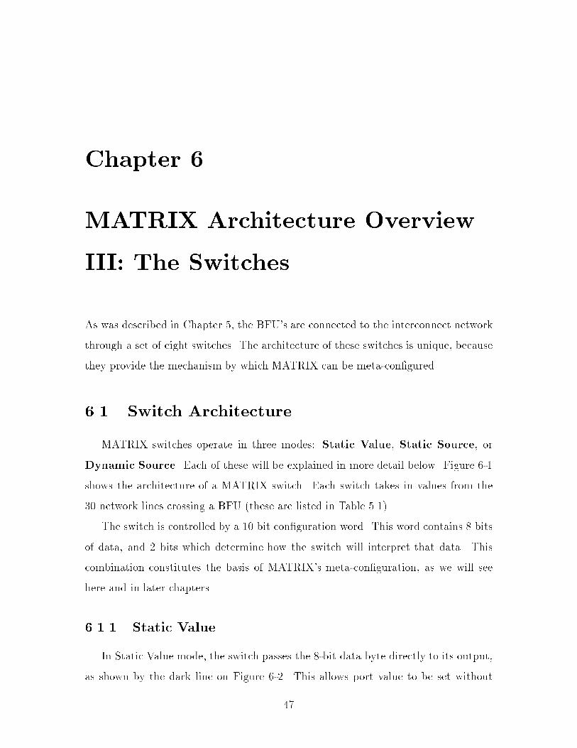
Chapter 6MATRIX Architecture OverviewIII: The SwitchesAs was described in Chapter 5, the BFU's are connected to the interconnect networkthrough a set of eight switches. The architecture of these switches is unique, becausethey provide the mechanism by which MATRIX can be meta-con�gured.6.1 Switch ArchitectureMATRIX switches operate in three modes: Static Value, Static Source, orDynamic Source. Each of these will be explained in more detail below. Figure 6-1shows the architecture of a MATRIX switch. Each switch takes in values from the30 network lines crossing a BFU (these are listed in Table 5.1).The switch is controlled by a 10 bit con�guration word. This word contains 8 bitsof data, and 2 bits which determine how the switch will interpret that data. Thiscombination constitutes the basis of MATRIX's meta-con�guration, as we will seehere and in later chapters.6.1.1 Static ValueIn Static Value mode, the switch passes the 8-bit data byte directly to its output,as shown by the dark line on Figure 6-2. This allows port value to be set without47

5
1
10
8 1
Level−1
Level−2
Level−3
Local Output1x8
8x8
8x8
88
12x8
1x8
Net
wo
rk I
np
uts
30
x8
Control Byte
Floating Port
Configuration
WordStatic/Dyanmic
Constant/Source
Data/Source Address
1 bit 1bit 8 bits
Dynamic Control Input
BFU Port
Figure 6-1: MATRIX Dynamic Switch Architecture5
1
10
8 1
Level−1
Level−2
Level−3
Local Output1x8
8x8
8x8
88
12x8
1x8
Net
wo
rk I
np
uts
30
x8
Control Byte
Floating Port
Configuration
Word
1 bit 1bit 8 bits
Dynamic Control Input
Static Value Data
BFU Port
Figure 6-2: MATRIX Switch in Static Value Mode48

5
1
10
8 1
Level−1
Level−2
Level−3
Local Output1x8
8x8
8x8
88
12x8
1x8
Net
wo
rk I
np
uts
30
x8
Control Byte
Floating Port
Configuration
Word
1 bit 1bit 8 bits
Dynamic Control Input
Static Source Source Address
BFU Port
Figure 6-3: MATRIX Switch in Static Source Modeconsuming network wires. For example, if a BFU is always performing add opera-tions, the add instruction would be programmed into the con�guration word for theFa Port's switch, and the switch set to static value mode. This will �x the ALU oper-ation to add without consuming network lines to broadcast that instruction. This isespecially useful for the FmPort because, as was discussed in Chapter 4, the functionscontrolled by this port are often constant during normal operation.In addition to �xed instructions, this mode can be used to assert constant memoryaddresses or insert speci�c constants into the BFU data ports, or onto the the network.6.1.2 Static SourceIn Static Source mode, the switch uses 5 bits of the data byte to select one of theincoming network lines to pass its data onto the BFU port. Figure 6-3 shows thepaths used in this mode. This mode allows the data, instruction, and control pathsthrough the network to be statically set as part of the meta-con�guration.6.1.3 Dynamic SourceIn Dynamic Source mode, the switch allows an outside source to control the cycle-49
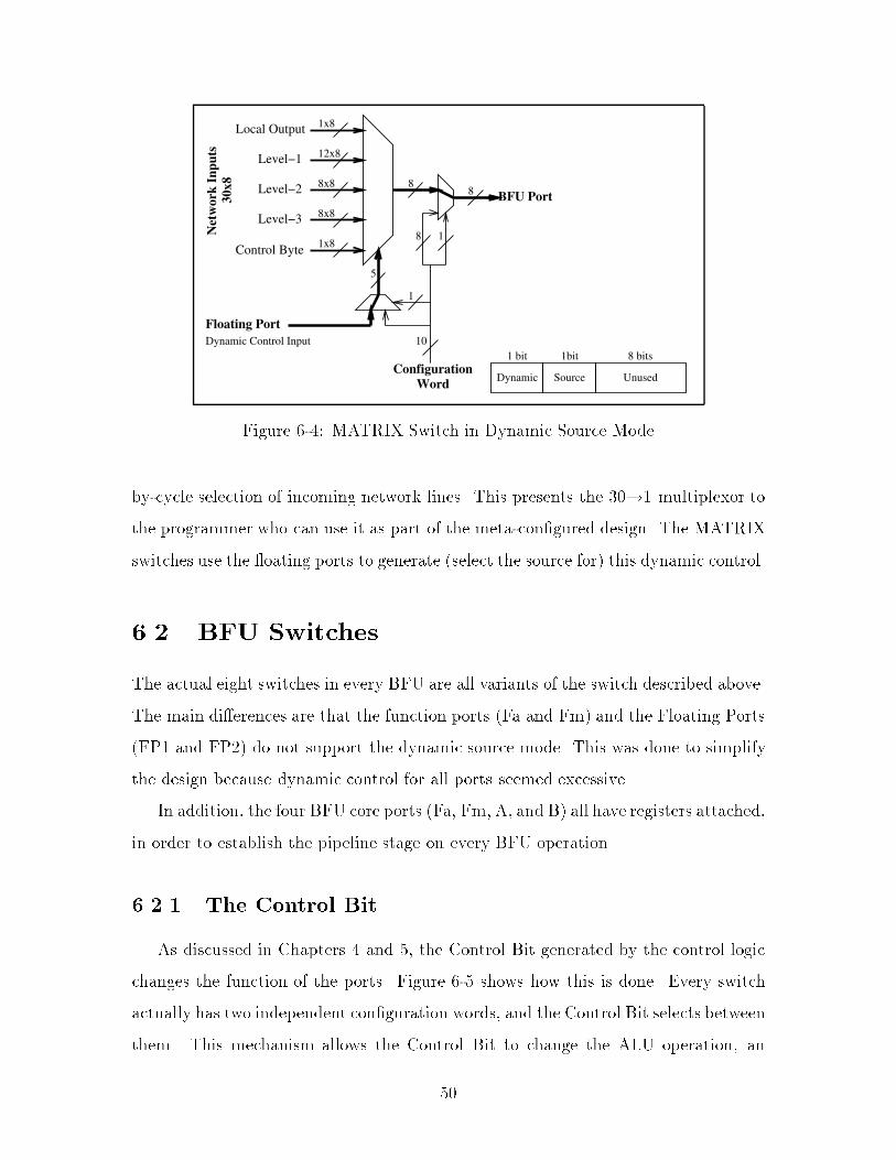
5
1
10
8 1
Level−1
Level−2
Level−3
Local Output1x8
8x8
8x8
88
12x8
1x8
Net
wo
rk I
np
uts
30
x8
Control Byte
Floating Port
Configuration
Word
1 bit 1bit 8 bits
Dynamic Control Input
Dynamic Source Unused
BFU Port
Figure 6-4: MATRIX Switch in Dynamic Source Modeby-cycle selection of incoming network lines. This presents the 30!1 multiplexor tothe programmer who can use it as part of the meta-con�gured design. The MATRIXswitches use the oating ports to generate (select the source for) this dynamic control.6.2 BFU SwitchesThe actual eight switches in every BFU are all variants of the switch described above.The main di�erences are that the function ports (Fa and Fm) and the Floating Ports(FP1 and FP2) do not support the dynamic source mode. This was done to simplifythe design because dynamic control for all ports seemed excessive.In addition, the four BFU core ports (Fa, Fm, A, and B) all have registers attached,in order to establish the pipeline stage on every BFU operation.6.2.1 The Control BitAs discussed in Chapters 4 and 5, the Control Bit generated by the control logicchanges the function of the ports. Figure 6-5 shows how this is done. Every switchactually has two independent con�guration words, and the Control Bit selects betweenthem. This mechanism allows the Control Bit to change the ALU operation, an50

5
FPout
1
10
8 1
Level−1
Level−2
Level−3
Local Output1x8
8x8
8x8
88
12x8
1x8
R
Net
wo
rk I
np
uts
30
x8
Control Byte
Control Bit
Configuration
Word A
Configuration
Word B
Register onA,B Ports Only
BFU (A,B)Network Drivers (N1,N2)
Figure 6-5: Switch Architecture with Control Bitinput constant, a memory address, or even the datapath/control ow. If no changeis desired, the same data can be programmed in both con�gurations. Its importantto remember that a BFU's Control Bit changes the operation of all eight switchessimultaneously.6.3 Con�guration Memories and ProgrammingChapter 4 described how the BFU's con�guration memorieswere programmed throughthe Con�guration Memory Read/Write Enable bits in the Fm Port. The di�cultywith this system is that it requires the port con�guration to exist in a known stateat startup, so it is possible to route the address/data pairs, as well as the enablesthemselves, to the BFUs. In MATRIX this is accomplished by giving all of the con-�guration memories on the chip several Global Contexts.In the current prototype there are four such contexts, as shown in Figure 6-6.Two of these (Contexts 2 and 3) are programmable, while the other two (Contexts 0and 1) are hardwired. 51

Global Context Select
Ctx 0 Ctx 1
Global Mode Select
Configuration Word
Ctx 2 Ctx 3
Hardwired ProgrammableFigure 6-6: Con�guration Memory StructureThe hardwired contexts used to bootstrap the chip. When set to Context 0, aMATRIX chip looks like a memory chip in write mode, so an external device cangenerate address/data pairs to program both the con�guration memories as well asthe main memories. Context 1 sets to the chip to act a memory in read mode, sothat a con�guration state can be o�oaded. More sophisticated uses of the hardwiredcontexts are possible, such as a machine that will automatically load con�gurationsfrom a passive memory o�-chip, or even complete designs to manage system-levelstartup issues. For the sake of simplicity, these were not implemented in the initialprototype.The programmable contexts are the ones used to hold meta-con�gurations foruser applications. When originally conceived, MATRIX was intended to have a\background-load" feature. This would allow a second meta-con�guration to beloaded while another was in use. The new design could then be swapped into opera-tion in a single cycle, allowing MATRIX to change algorithms or even entire designsrapidly. This turned out to be too complicated for the initial prototype. The cur-rent design still allows designs to be rapidly swapped out, only now they cannot bere-loaded without interrupting a running design.52

Chapter 7Prototype ImplementationThe MATRIX prototype is being implemented in a 0.5�m, 3 metal layer CMOSprocess. A complete BFU has been designed and oorplanned, and results of thiswill be described below. However, timing analysis of the circuitry has not yet beencompleted, so timing results are not available at this writing. Initial estimates suggestthat this prototype will be able to achieve a 10ns (100Mhz) cycle time.One of the main goals of the layout was to keep the BFU as small as possible. Aswe will see in Chapter 8, the performance of a MATRIX chip of a given size is directlyrelated to the number of BFUs that can be �t on it. The original targeted BFU sizewas 1mm�1mm. As we will see, this turned out to be too di�cult to accomplish onthis �rst pass design.7.1 FloorplanFigure 7-1 shows the oorplan design for a MATRIX BFU. The design evolvedfrom the BFU block diagram (Figure 4-1), with the main memory in the top centerand the switches feeding addresses and data in from the sides.Figure 7-2 shows how the network wires travel across the BFU. The blue lines(dark grey) are horizontal, red lines (light grey) represent the vertical wires. Data onthe wires is switches in the eight switches, and travels down to the registers. Fromthe registers the data is passed to the rest of the BFU, including the memory and53

ConfigurationMemory
Multip
lier
ControlLogic
AL
URegisters Registers
Main Memory
ConfigurationMemory
Network Drivers
OR Plane
Netw
ork
Sw
itch
es
Netw
ork
Sw
itch
es
Figure 7-1: BFU FloorplanConfiguration
Memory
Multip
lier
ControlLogic
AL
URegisters Registers
Main Memory
ConfigurationMemory
Network Drivers
OR Plane
Netw
ork
Sw
itch
es
Netw
ork
Sw
itch
es
Figure 7-2: Network Wires Over A BFU54

Component Dimensions (�m) Area (�m2) PercentageBFU 1500�1200 1.8M 100%MainMem 755�620 468,100 26%ALU 230�265 60,950 3.4%Multiplier 215�265 56,975 3.2%Switches (700�67)�8 375,200 20.8%Switch Con�g (284�67)�8 152,224 8.5%Registers (186�67)�8 99,696 5.5%ORplane 1050�100 105,000 5.8%C/R I (60�50)�9 27,000 1.5%C/R II (60�50)�21 63,000 3.5%Drivers,Misc Logic, 21.8%Unused Area Table 7.1: BFU Area ResultsALU.The oorplan shown in Figure 7-1 is certainly not an optimal layout. For example,if the switches, registers and switch con�guration memories were built together, theoverall structure would be smaller, and probably faster, due to the large amount ofwiring currently used to connect these units.However, even the current BFU design does not result in poor performance. ABFU of 1.2mm�1.5mm allows a MATRIX chip consisting of a 10�10 array of BFUsto be fabricated in a reasonable die size. A MATRIX chip of this size would have araw performance of 10 billion (8-bit) operations per second.7.2 Area ResultsTable 7.1 shows the breakdown in area usage of the BFU components. The wholeBFU is approximately 1.2mm�1.5mm. Some of the signi�cant results of this are:� The main memories account for 26% of the whole BFU area. This means thatthe 256x8 bit size is not too large for this BFU. However, if the BFU were tobecome smaller, this size will become quite signi�cant. in a 1mm�1mm BFU,this memorywould consume nearly 47% of the area. Under those circumstances,55

either a tighter memory design, or a smaller memory size would be required.� The switches, and their associated con�guration memories and registers accountfor 34.8% of the current BFU. This amounts to over 4% per switch. If the BFUhad been its targeted size, this would be nearly 63%, or nearly 8% per switch.Clearly, a tighter layout would be required in order to make the BFU smaller.Another possibility would be to reduce the size of the switches themselves. Ifeach switch took 15 inputs, instead of 30, the switches would fall to under 25%of the current BFU size, or 44% of the 1mm�1mmBFU. If this option is chosen,the network would have to be redesigned (which may be a good thing), becausethere would be a large degree of asymmetry in which network lines were visibleto the BFU.� The actual computing logic is only 6.6% of the current BFU, or almost 12% ofa 1mm�1mm BFU. Compared to the other component this is almost insignif-icant. However, even though more functionality may balance the situation, itsprobably more advantageous for the whole chip to reduce the size of the othercomponents instead of increasing the ALU.� The multiplier essentially doubles the size of the current ALU, but since theALU is so small (in comparison with everything else), the addition of the mul-tiplier was a net win.56

Chapter 8MATRIX Application Example:FIRIn order to illustrate how MATRIX works, this chapter will examine a simple applica-tion in depth. The application used is a Finite Impulse Response (FIR) convolution,a common primitive in signal processing. The problem is to take a set of k weightsfw1, w2, : : : wkg and a sequence of samples fx1, x2,: : :g, and compute a sequence ofresults fy1, y2,: : :g according to:yi = w1 � xi + w2 � xi+1 + � � � + wk � xi+k�1where each wk �xi is called a Filter TAP. These examples are based on 8-bit sampledata (xi) and a 16-bit accumulate (yi).8.1 Comparison BenchmarkIn order to compare the e�ciency and performance of MATRIX designs with moreconventional architectures, we will employ the metric of functional density, similarto the one used in [5]. Functional density measures the capacity per unit area ofI am indebted to Andr�e DeHon for working through the details of these examples. This material�rst appeared in [13]. 57

a device. The capacity of a device is roughly the number of unit operations it canperform in a unit of time.In this case, we will measure the number of �lter TAPs per unit area. We willuse the second (s) as the unit of time. The unit area will be in terms of �2, where� is one-half the minimum feature size of the process used (a 1�m process wouldhave a � of 0.5�m). This will help to eliminate advantages due to superior processtechnologies so we can evaluate devices in terms of their architectures only. Theresulting benchmark looks like: Filter TAPs�2 � sThe advantage of using a capacity-based measurement, especially when processtechnology variations have been normalized out, is that we can compare the e�ciencywith which an architecture utilizes its silicon area for a the given task. Because theamount of normalized silicon area used is directly related to the raw cost of fabricatinga chip, this measurement can be viewed as a kind of price/performance benchmarkrather than one of the maximum performance benchmarks traditionally used.For all these examples we will be assuming a MATRIX BFU is 1.2mm�1.5mm,in a 0.5�m process (as shown in Chapter 7), giving it a size of � 29M�2. We willassume a clock rate of 100MHz, giving a 10ns cycle.8.2 Systolic - Spatial FIR8.2.1 ImplementationFigure 8-1 shows a purely systolic or spatial implementation of the FIR �lter, witheight TAPs (k = 8). Every block in the array is a BFU con�gured to act as labeled.The top row simply acts a staged pipeline, carrying the input down the row at onecycle per step. The multiply cells perform the 8�8 multiplication against hardcodedweights. The lower two rows accumulate the 16-bit results of the multiply operations.This example uses the BFU ports in Static Value mode to set the function of58

Add
Pass
Add
Mult
Add
Pass
Add
Mult
Add
Pass
Add
Mult
Add
Pass
Add
Mult
Add
Pass
Add
Mult
Add
Pass
Add
Mult
Add
Pass
Add
Mult
Add
Pass
Add
Mult
x i
y i
(8 bit)
(16 bit) Figure 8-1: Systolic FIR Implementationeach of the BFUs as well as the weights on the multiply operations. In addition,Static Source mode is used on the data inputs to de�ne the datapaths (the arrows inFigure 8-1).The performance limiting step in this case is the multiply operation because ittakes two cycle to complete the 16 bits of result. As a result, new inputs can only befed in every other cycle, giving a throughput of 50MHz.The implementation in Figure 8-1 uses 4 BFUs per �lter TAP, but a more involvedimplementation could:� Use the horizontal Level-2 lines for pipelining the inputs, removing the need forthe top row of BFUs simply to carry sample values through the pipeline.� Use both the horizontal and vertical Level-2 lines to retime the data owingthrough the add pipeline so that only a single BFU adder is needed per �ltertap stage. This is an example of an unplanned use of the Level-2 lines� Use three I-stores and a program counter (PC) to control the operation of themultiply and add BFUs, as well as the advance of samples along the samplepipeline. This design would be a hybrid between the systolic implementationand the microcoded example in Section 8.3.59

Device MATRIX FPGA (XC4K)Reference ICSPAT93 [4] App. Note [8]Size 2 BFUs/TAP 100 CLBs/TAP 67 CLBs/16-TAPs29M�2/BFU 1.25M�2/CLBSpeed 20 ns cycle 100 ns cycle 184 ns cycleDensity 0.87/�2 � s 0.08/�2 � s 1.0/�2 � sTAPs=�2 � s (symmetric)Table 8.1: Systolic FIR Performance Density ComparisonThus, the k-weight �lter can be implemented with only 2k + 4 cells in practice.8.2.2 Performance DensityTable 8.1 shows a density comparison between the MATRIX systolic FIR imple-mentation and two other systolic FIR implementations, both done on Xilinx 4000-series FPGAs. The second FPGA design is restricted to symmetric weights, whileboth MATRIX and the �rst FPGA design can use fully exible weights.Using an average of 2 BFUs per TAP, at 50MHz, MATRIX compares favorablyeven to the symmetric-weight FPGA design, and is a factor of 10 more dense than amore typical FPGA design. In addition it has a much higher overall throughput.8.2.3 ConclusionsAs we will see, systolic designs can achieve the highest raw performance density of anydesign styles on a general-purpose computing architecture. However, there are twomain drawbacks to systolic designs. First of all, they require resource to be allocatedfor every operation to be performed. In this case, 2 BFUs are required for everyTAP desired, regardless of the clock rate. This sets a minimum area for these designswhich can grow to be quite large for many TAPs.The second drawback is also related to the minimum area. If the application'srequired throughput is lower than that provided by the design, the design's yieldedperformance density decreases from the peak performance. For example, if an appli-60

ALU
PC
bI
aluI
mfI
srcI
srcI
y i
x i(8 bit)
(16 bits output over 2 cycles)
aI
Figure 8-2: Microcoded FIR Implementationcation required an FIR at 25MHz, the MATRIX design would yield at � 0:4 � �2 � s.1Systolic designs have no means of taking advantage of the extra time alloted.8.3 Microcoded - Temporal FIR8.3.1 ImplementationFigure 8-2 shows a microcoded design of an FIR �lter. Rather than dedicatingBFU to performing dedicated functions, one BFU is being used to perform all therequired operations (the blue (dark grey) BFU marked \ALU"). The BFU's mainmemory is being used as a register �le to store the coe�cient weights (wk) as well assix intermediate variables.Six additional BFUs are used as instruction stores to hold the microcoded pro-gram. These BFUs use their main memories as 256 byte blocks, and do not use theirALUs for any computation. The purpose of each are as follows:Ia and Ib are used to store the A and B register addresses.Ialu and Imf are used to store the ALU operation, and FmPort function, respectively.The Isrc memories control the dynamic behavior of the A and B ports (through theFP1 and FP2 ports). This is an example of ports being used in Dynamic Source1It may be worth noting that neither FPGA implementations could achieve this rate all.61

Label ALU Op PCnewsample Rxp Rxp + 1 ; Match (k + 1) (6 bits) BNE xpcont1< Rxp > new xi (pipelined branch slot)Rxp 65xpcont1 < Rxp > new xiRs < Rxp >Rwp 1Rw < Rwp >Rs Rs � RwRw �-continueRl Rs; Match false BNE enterloopRh Rw (pipelined branch slot)innerloop Rs Rs � RwRw �-continueRl Rs + RlRh Rw +-continue Rhenterloop Rxp Rxp + 1 ; Match (k + 1) (6 bits) BNE xpcont2Rs < Rxp > (pipelined branch slot)Rxp 65Rs < Rxp >xpcont2 Rwp Rwp + 1 ; Match (k + 1) (6 bits) BNE innerloopRw < Rwp > (pipelined branch slot)last read Rl ; Match false BNE newsampleread Rh (pipelined branch slot)Table 8.2: Microcode for FIR Computationmode. During normal operation, the A and B ports are being used to supplythe register addresses for the internal calculation. However, in order to loada new sample value, these ports must switch to loading data from an externalsource. This is accomplished using the dynamic port mode on the A and Bports.Finally, a single BFU has been con�gured to supply the lookup address for theI-stores. This Program Counter (PC) is setup to either increment its counter, or loada new counter value from its internal memory, based on the current operational step.Table 8.2 shows the microcode for the FIR computation. The 8 BFUs shown inFigure 8-2 produce a new 16-bit result every 8k + 9 cycles (k is the number of �lterTAPs). The result is output over two cycles. In this example, k � 61 because ofthe limited space in the ALU's register �le memory. Larger FIRs could be supportedusing additional BFUs to store the extra sample and coe�cient values.62

Device MATRIX MIPS-X NEC VSP8 1996 Alphamstep 32b mpy 64b mpyReference ISSCC87 [10] [14] ISSCC96 [9]Size 8 BFUs 1 die 1 die 1 dieArea 29M�2/BFU 68M�2 1.2G�2 6.8G�2Clock Rate 10 ns cycle 50 ns cycle 10 ns cycle 2.3 ns cycleThroughput 8 cycles/TAP 10+ cycles/TAP 4 cycles/TAP 1 cycle/TAPDensity 0.054/�2 � s 0.029/�2 � s 0.022/�2 � s 0.064/�2 � sTAPs=�2 � sTable 8.3: Microcoded FIR Performance Density Comparison8.3.2 Performance DensityTable 8.3 compare the performance density of the microcoded MATRIX designwith three modern microprocessor architectures. Of these, the NEC VSP8 and theDEC Alpha have hardwired multipliers, while the MIPS-X has only a multiply-stepoperation. As we can see, MATRIX compares very well to these designs, beating outall but the Alpha.The main reason the microprocessors performed poorly against the MATRIX de-sign, is the fact that they tied up their entire chip performing the simple 8-bit FIR,while MATRIX was able to free whatever space remained on the die to performingother operations. This demonstrates the one of the main ine�ciencies of traditionalmicroprocessor architectures: unneeded on-chip resources are wasted when not inuse. In modern microprocessors, a large amount of chip area is dedicated to cachesdesigned to handle rapidly changing, random instruction streams. On regular appli-cations such as FIR this area goes mostly unused. In addition the large datapathwidths (64 bits on the Alpha) are unneeded in this 8-bit FIR example.18.3.3 ConclusionsMicrocoded designs provide a mechanism for reusing functional blocks to performmultiple operations in time. As a result they are very useful when there is a lim-1This is not an unreasonably small size - most signal processing applications require FIRs nolarger than 16 bits. 63

Xptr
wI
xI
srcI aluIPC
WptrX +
aluI Ia
y i
x i (8 bit)
(16 bits output over 2 cycles)Figure 8-3: Custom VLIW FIR Implementationited amount of space available. In fact, microprocessor architectures were originallyconceived as a method of e�ciently using the very limited (at the time) silicon areaavailable. However, modern microprocessors do not su�er this restriction, yet con-tinue to follow the same design methodology. As a result, their performance densityhas su�ered in comparison to other architectures.The major drawback for microcoded designs is that due to the need to performall operations on a single unit, every application will require a minimum amount oftime to run. One possible solution to this was mentioned in Section 8.2 - create ahybrid systolic/microcoded design. In such a design, the systolic logic would handlethe high required throughput portions of the application, while the microcoded logicwould handle the control and infrequently needed functions. The combination of thetwo would be smaller than a pure systolic array, but faster than a pure microcodeddesign.Another possible solution is presented in Section 8.4, below.8.4 Custom VLIW FIR8.4.1 ImplementationFigure 8-3 shows a custom VLIW implementation of an FIR �lter. This exam-ple takes advantage of the parallism inherent in the FIR computation to constructapplication-speci�c datapaths, while maintaining a temporal computing style.As shown in Figure 8-3, there are four BFU allocated to performing computation:64

Label Xptr unit Wptr unit MPY unit +-unit�rstsample Xptr 64 Wptr 0output Xptr output Wptr < Xptr > new xinextsample Xptr++ mod k j 64 Wptr++ < Xptr > � < Wptr >output Xptr output Wptr �-continue Rlow MPY-resultXptr++ mod k j 64 Wptr++ < Xptr > � < Wptr > Rhigh MPY-resultoutput Xptr output Wptr �-continue Rlow Rlow + MPY-resultinnerloop Xptr++ mod k j 64 Wptr++; Match k < Xptr > � < Wptr > Rhigh Rhigh + MPY-resultoutput Xptr output Wptr �-continue Rlow Rlow + MPY-resultlast output Xptr output Wptr < Xptr > � < Wptr > Rhigh Rhigh + MPY-resultXptr++ mod k j 64 Wptr 0; Match false �-continue Rlow Rlow + MPY-resultoutput Xptr output Wptr < Xptr > new xi Rhigh Rhigh + MPY-resultTable 8.4: VLIW Microcode for FIR Computationone each for the multiply and add operation, one to manipulate the sample pointer(Xptr), and one to manipulate the coe�ent pointer (Wptr). There are also six BFUsallocated as instruction stores, and one BFU for serve as a program counter. Thisarrangement makes it possible to reduce the inner loop of the FIR computation totwo steps, as shown in Table 8.4. The boxed values in last column are the pair of yioutput bytes at the end of each convolution.As shown in Figure 8-3, this implementation requires 11 BFUs and produces anew 16-bit result every 2k + 1 cycles. As in the microcoded example the result isoutput over two cycles on the ALU output bus. The number of weights supported islimited to k � 64 by the space in the ALU's memory.Most of the I-stores used in this design contain only a few instructions. With cleveruse of the control PLA and con�guration words, the number of I-stores can be cutin half making this implementation no larger than the microcoded implementation,while still being four times faster.8.4.2 Performance DensityTable 8.5 compares the performance density of the MATRIX VLIW FIR imple-mentation with a modern DSP chip. The DSP uses a similar VLIW approach toperforming FIR computations. In this case, the DSP's slower clock rate and largerarea gave it a signi�cantly lower performance density. While DSPs have tailoredtheir datapath to performing signal processing operations, they include many morehardwired functional units, most of which are not needed for a given application.65

Design MATRIX Toshiba 16b DSPReference CICC92 [17]Size 11 BFUs 1 dieArea 29M�2/BFU 275M�2Clock Rate 10 ns cycle 50 ns cycleThroughput 2 cycles/TAP 1 cycle/TAPDensity 0.16/�2 � s 0.072/�2 � sTAPs=�2 � sTable 8.5: VLIW FIR Performance Density Comparison8.4.3 ConclusionsThis example demonstrates the advantages of customizing a datapath to an individualapplication. The VLIW approach to a problem improves the performance of temporaldesigns with a usually minimal area cost.8.5 Hybrid FIR ArchitecturesMicrocoded and VLIW designs allow MATRIX to take advantage of a lower desiredthroughput to reduce the chip area required for the computation. This saved areacould be used to perform other computations, or could be used to perform the samecomputation in parallel. For example, a MATRIX chip with 64 BFUs could, theo-retically, perform 8 microcoded, or 5 VLIW, FIR computations in parallel simply bydedicating a separate microcoded design to each FIR.If each FIR computation is running at a di�erent rate, or in di�erent time-steps,this is the best that can be done. However, if the FIRs can be run in lock-step, adrastic improvement can be made. Figure 8-4 shows a Multiple-SIMD/VLIW hybridFIR Implementation. A single VLIW control structure, running the code shown inTable 8.4, controls 6 parallel FIR computations. The whole structure requires 21BFUs which is one-third the size of 6 independent VLIW designs.Many other hybrids are possible, depending on the exibility and requirementsof speci�c applications. Hardware optimizations like these are only possible onMATRIX-like architectures which allow users to completely de�ne the computing66

Xptr
wI
xI
srcI aluIPC
Wptr
aluI Ia
X
+
X X X X X
+++++
ix1
y1 i
ix2
y2 i y3 y4 iy6
x6 ix4 ix3 i
i i y5 i
x5 i
Figure 8-4: VLIW/MSIMD Hybrid FIR Implementationstructure that ideally suits the problem.8.6 SummaryTable 8.6 shows the performance density results for the FIR example running onseveral di�erent architectures. The \XC4K" is a Xilinx 4000-series FPGA. A CLBis a 4!1 combinational logic block, the basic unit of Xilinx FPGAs. PADDI2 is anexperimental MIMD device with 16-bit execution units (EXUs). Two fully customFIR chips have been included for comparison.As we can see, MATRIX designs are comparatively dense, or even better, thansimilar architectures. In addition, as we have seen, MATRIX has the ability tochange its design to match application requirements and exibility, giving it a robustperformance density across a wide range of applications.67

Architecture Reference Area and Time Filter TAPs�2�s16b DSP ISSCC86 [21] 125 ns/TAP 0.090CICC92 [17] 50 ns/TAP 0.07232b RISC mstep MIPS-X [10] 50+ ns/TAP 0.02932b RISC/DSP VSP8 [14] 40 ns/TAP 0.02264b RISC 1996 Alpha [9] 2.3 ns/TAP 0.064systolic 2 BFUs, 20ns/TAP 0.87MATRIX microcode 8 BFUs, 80ns/TAP 0.054VLIW 11 BFUs, 20ns/TAP 0.16XC4K App. Note [8] 64 CLBs, 184 ns/16-TAPsy 1.0ICSPAT93 [4] 400 CLBs, 100ns/4-TAPs 0.080PADDI2 ISSCC95 [22] 5 EXUs, 20ns/TAP 0.93Full Custom JSSC89 [16] 45ns/64-TAPsz 6.1JSSC90 [7] 33ns/16-TAPs 3.5y { symmetric �lter; z { 24-bit accum.Table 8.6: FIR Survey - 8�8 multiply, 16-bit Accumulate68
Chapter 9Relationship to ConventionalComputing DevicesAs we have seen, MATRIX is capable of changing its architectural structure in orderto match application needs. This makes the task of comparing it to other conven-tional architectures which cannot change their structure di�cult. Table 2.1 classi�edconventional architectures by the instruction/control allocation choices they made(Chapter 2). This chapter will examine these architectures and compare the choicesthey made with MATRIX implementations of those architectures.9.1 Systolic ArchitecturesAs discussed in Chapter 2, systolic architecture compute spatially, and therefore donot have any control threads. Table 2.1 list three di�erent kinds of systolic architec-tures:Hardwired Functional Units are included here as a special case since they arenot general-purpose architectures. Hardwired units �x all of their functionalitychoices at fabrication time, and are not programmable.FPGAs are �ne-grain programmable systolic arrays. Due to their granularity, theytypically have a large number of basic units on a die (large n). Due to its69

Diff
Sub
Min Min
Min Position
Position Count
Diff Diff Diff
Sub
Sum SumSum Sum
Figure 9-1: Best Match Detector - Systolic Arraybasic 8-bit granularity MATRIX cannot implement these architectures, but willgenerally perform much better against FPGAs implementations of coarser-graincomputations.Recon�gurable ALUs are coarse-grain programmable systolic arrays. At �rst glance,a MATRIX array looks a great deal like these devices, especially when pro-grammed to perform systolic operations. Figure 9-1 shows an example of aMATRIX array acting as an array of recon�gurable ALUs. The computationshown is a best-match detector used in video compression applications.While MATRIX can act like an array of recon�gurable ALUs (at a multiple-of-8granularity), it is not a systolic array because of its ability to temporally reuseits resources. As we saw in Chapter 8, this ability allows MATRIX to takeadvantage of application exibility in ways traditional systolic arrays cannot.9.2 Traditional and SIMD ProcessorsMoving down on Table 2.1, we begin to see devices that temporally reuse their re-sources. The �rst three types of these are traditional microprocessors and SIMD70

F A BPC
ALU ALU ALU ALUFigure 9-2: 32 Bit Microprocessor(Single Instruction, Multiple Data) or Vector (essentially wide-datapath SIMD) pro-cessors. These three are similar in that they each have only one instruction streamon the device.Traditional processors use a single, usually very coarse grain (w = 32 or 64 bit)ALU. Figure 9-2 shows an example of a (simple) traditional microprocessor architec-ture implemented on MATRIX. The MATRIX implementation composes the 32-bitdatapath from 4 BFUs by creating a carry-chain. Three other BFUs store the 24-bitinstruction ([A op B ! A] style operations), and one BFU serves as the programcounter.In a similar manner, MATRIX can implement a SIMD or Vector machine. A singleprogram counter and set of instruction stores can control any number of processors,as shown in Figure 9-3. MATRIX cannot emulate a bitwise SIMD array due tothe 8-bit granularity of the BFU, but it can implement a SIMD or Vector machinebuilt from multiple-of-8 datapaths. Datapaths are assembled by composing BFUsthrough carry-chains. We saw an application-speci�c example of this processing stylein Chapter 8.A number of other architectures have been proposed or built which can also adjust71

APCF B
ALU ALU ALU ALU
ALU ALU ALU ALU
ALU ALU ALU ALUFigure 9-3: SIMD Systemto di�erent datapath granularity. Typically, this is accomplished through segmentabledatapaths (e.g. [19] [1]). These generally exhibit SIMD instruction control for thedatapath, but can be recon�gured to treat the n bit datapath as k, nk -bit words, forcertain, restricted, values of k. Modern multimedia processors (e.g. [18] [6]) allowthe datapath to be treated as a collection of 8, 16, 32, or 64 bit words.All of these architectures give users the ability to choose an appropriate granularityfor their computation. However, they all control these datapaths in a SIMD manner.MATRIX allows not only exible data-widths, but exible control, as we will see inthe following sections.9.3 Multi-Context Gate Arrays and VLIW Ma-chinesAnother group of device that have a single on-chip instruction thread are multi-context gate arrays and VLIW (Very Long InstructionWord) machines. These devicesare categorized by having multiple instruction stream operating under a single threadof control. 72

PC
F
ALU
A
B
F
ALU
A
B
F
ALU
A
B
Figure 9-4: VLIW SystemMulti-context gate arrays are FPGA-like devices which store multiple instruction(con�gurations) on-chip. Several designs have been proposed including: the DPGA[20] which provides a small number of instructions per basic look-up table (4 inthe current prototype), and VEGA [11] which provides 2048 instructions.1 Thesedevices all �x the number instructions on-chip at fabrication time, making it hardselect the \correct" size of the instruction memories. While MATRIX cannot matchthe �ne-grain datapaths of the DPGA and VEGA, it can exibly deploy instructionmemories (in 256 instruction chunks, on the current prototype) to more closely matchan application's requirements.VLIW machines are essentially coarse-grain versions of multi-context gate arrays(or that the multi-context gate arrays are �ne-grain VLIW machines). Figure 9-4shows a generic VLIW machine implemented on MATRIX. A single program counter(PC) controls three separate instruction streams. As discussed in Chapter 2, thesedesigns generally provide more processing power per unit area than MIMD machines,but do not have the same control exibility.Various architectures, such as PADDI [3] choose a granularity (16 for PADDI),1VEGA actually has multiple program counters and therefore functions as a MIMD machine.73

F A BPC
ALU ALU ALU ALU
F A BPC
ALU ALU ALU ALU
Figure 9-5: 32 Bit MIMD Systemand a instruction memory size (8 for PADDI). MATRIX allows a designer to choosethe VLIW architecture which best suits the application to the extent that the 8-bitBFU allows. We saw an example of this in Chapter 8.9.4 MIMD MachinesDevices utilizing more than one program counter (control unit) per die are con-sidered MIMD (Multiple-Instruction, Multiple-Data) machines. Figure 9-5 shows angeneric 2-PC, 32-bit MIMD machine implemented on MATRIX. Just as in the VLIWcase, a variety of devices, such as PADDI-2 [22], have chosen a speci�c data point,while MATRIX gives a designer the option of changing those choices.9.5 Hybrid ArchitecturesCertainly not all applications fall into one of the traditional computing realmsdiscussed above. In order to e�ciently deal with these cases a number of architectures,including MSIMD (e.g. [2], [15]) have been developed. These devices allocate controlunits among a set of processing units. Like MATRIX, these devices can deploy control74

A PC
FB
ALU ALU
ALU ALU
A PC
FB
ALU ALU
ALU ALUFigure 9-6: MSIMD Systemunits as applications require. Unlike MATRIX, the control and processing units arenot the same, nor do data and control travel over the same network. This limits thestructure and exibility of any resource allocation. Figure 9-6 shows an example ofone possible MSIMD design on a small MATRIX array.Many hybrid architectures are possible on MATRIX. We saw an application-speci�c example of one in Chapter 8.9.6 SummaryAs we have seen in these examples, MATRIX covers nearly all the architectural pos-sibilities listed in Table 2.1, as well as many that are not listed there. All the deviceslisted on the table �x their place in the taxonomy at fabrication time. MATRIX,on the other hand, can use its meta-con�gurability to implement nearly any of thosestructures, and therefore cannot be �t into that classi�cation.75

Chapter 10Conclusions10.1 ResultsThe MATRIX prototype demonstrates the possibilities for meta-con�gurable archi-tectures. These include:� High Performance { The prototype architecture can support designs thatachieve a similar performance density to conventional commercial and academicdevices with similar computing styles.� Flexibility { The MATRIX architecture can implement nearly any kind oftraditional architecture, while not �tting into any traditional classi�cation.� Architectural Advantages { MATRIX achieves its performance and exibil-ity without relying on exotic manufacturing technologies, and can therefore ridethe process technology curve along with all other architectures.On the downside, MATRIX is so di�erent from traditional architectures that stan-dard methods of programming do not easily apply. MATRIX allows the programmerto optimize the architecture while optimizing a program and the algorithm. Thismulti-dimensional space is very di�cult to search.It is always possible to implement a conventional architecture on MATRIX, thenprogram it normally. However, this does not allow the application to take advantage of76

MATRIX's meta-con�gurability and its performance will su�er accordingly. In orderfor meta-con�gurable architectures to come into widespread use, a new programmingmethodology is needed.10.2 Future WorkMeta-con�gurable architectures open up a very large space of architectures and sys-tems that has not yet been explored. The MATRIX prototype is simply a singledatapoint in this space. Some avenues for future exploration include:� Di�erent Granularities { While meta-con�guration does not make sense ata very small or very large granularity, there is still a wide range of basic gran-ularities that might work better than the 8 bits chosen for MATRIX.� Di�erent Internal Arrangement of the BFU { Perhaps a more exibleBFU structure would be able to better deploy some of its resources withoutconsuming others. For example, a di�erent BFU structure might make theALU available for computation even when the memory has been deployed as anI-store.� Di�erent Network Structures { Network structures that more accuratelyre ect the needs of applications, such as the inclusion of pipeline/retiming reg-isters, will certainly improve the usability of these devices� Hybrid Architectures { Coarse-grain blocks, such as the MATRIX BFU,are not well suited for �ne-grain control logic, and the distributed PLA is apoor substitute for real �ne-grain logic. Perhaps combining a MATRIX-likearchitecture with FPGA-like �ne-grain blocks would make creating control logicmuch easier.On the other hand, traditional microprocessor-like structures are very well-suited for handing random control manipulations. Instead of FPGA-like logic,perhaps the inclusion of a small microprocessor on a MATRIX array wouldprove worthwhile. 77

� Programming Tools { As mentioned above, the programming methodolo-gies required to create very high-performance designs on a meta-con�gurablearchitecture are very di�erent from traditional methods. A whole set of toolsneeds to be developed so that designs can be quickly and easily mapped tometa-con�gurable architectures like MATRIX.10.3 SummaryAll general-purpose computing devices can perform any operation, based on theirinstruction stream. However, traditional general-purpose computing devices cannotadapt the way in which they handle these instruction to match the application'srequirements. Because of this, these devices are e�cient only on a speci�c set ofapplications. MATRIX, on the other hand, supports a meta-con�guration layer whichallows applications to create a computing architecture which more closely matchestheir requirements. This is accomplished through:� Parallel, Con�gurable Data ow { Datapaths can be wired up in an application-speci�c manner allowing data to be delivered directly to their destinations,rather than requiring special, load/store-like operations to move the data.� As much Dynamic Control as Needed { Whenever an application needs tochange instructions or data on a cycle-by-cycle basis, resources can be allocatedto do so. On the other hand, when these things do not need to change, theycan be con�gured so they do not consume control or network resources, freeingthese resources for other needs.� As much Regularity as Exploitable { Every instruction can be broadcastto any number of functional units, so that regular operations do not consumeextra instruction memories and control units.� Deployable Resources { Each BFU and network switch has uni�ed instruc-tion control, datapath, and memory resources, which can be deployed as needed78

in an application. High-bandwidth applications, or parts of applications, can becomposed spatially, while low-bandwidth applications can save space by com-posing application temporally.These features allow MATRIX to yield high performance across a wide range ofapplications.
79
Appendix ABFU ModelThis appendix contains the Verilog code for a MATRIX BFU model. The codehas been debugged and tested on a wide range of input vectors. It will be part ofa complete MATRIX chip model, which will be used to run applications until theprototype chips are in.A.1 Top Level BFU Module/****************************//* Specifications for BFU.v *//****************************//* BFU is the model of a MATRIX BFU. See TN130 for details on its operationand I/O ports. (Hopefully all the names here will be the same as listedin TN130)The modules contained in this module are:BFUcore, CompReduceI, Config, Control, Fport, L1drivers, L2driver,L3decode, L3driver, MAdd, NAport, TSregister.A BFU has the following parameters:X, Y : The BFU's X and Y address in the array.*//*****************//* Include Files */ 80

/*****************/`include "BFUcore.v"`include "CarryDecode.v"`include "Config.v"`include "Control.v"`include "Fport.v"`include "L1drivers.v"`include "L2driver.v"`include "L3decode.v"`include "L3driver.v"`include "MAdd.v"`include "NAport.v"`ifdef CompReduce_defined`else`include "CompReduce.v"`endif`ifdef TSregister_defined`else`include "TSregister.v"`endif/**************//* Module BFU *//**************/module BFU(CLK, Gctx, start,L1_N1, L1_N2, L1_NE, L1_E1, L1_E2, L1_SE,L1_S1, L1_S2, L1_SW, L1_W1, L1_W2, L1_NW,CR_N1, CR_N2, CR_NE, CR_E1, CR_E2, CR_SE,CR_S1, CR_S2, CR_SW, CR_W1, CR_W2, CR_NW,Cin_N, Cin_E, Cin_S, Cin_W,L2_N1, L2_N2, L2_E1, L2_E2, L2_S1, L2_S2, L2_W1, L2_W2,L3_V1, L3_V2, L3_V3, L3_V4, L3_H1, L3_H2, L3_H3, L3_H4,L3_V1en, L3_V2en, L3_V3en, L3_V4en,L3_H1en, L3_H2en, L3_H3en, L3_H4en,L1_Nout, L1_Eout, L1_Sout, L1_Wout, CRout, Cout,L2_1out, L2_2out);/**************//* Parameters *//**************/parameter X = 0, Y = 0;/********************//* I/O Declarations *//********************/input [1:0] Gctx;input CLK, start; 81

input [7:0] L1_N1, L1_N2, L1_NE, L1_E1, L1_E2, L1_SE;input [7:0] L1_S1, L1_S2, L1_SW, L1_W1, L1_W2, L1_NW;input CR_N1, CR_N2, CR_NE, CR_E1, CR_E2, CR_SE;input CR_S1, CR_S2, CR_SW, CR_W1, CR_W2, CR_NW;input Cin_N, Cin_E, Cin_S, Cin_W;input [7:0] L2_N1, L2_N2, L2_E1, L2_E2, L2_S1, L2_S2, L2_W1, L2_W2;inout [7:0] L3_V1, L3_V2, L3_V3, L3_V4, L3_H1, L3_H2, L3_H3, L3_H4;input [3:0] L3_V1en, L3_V2en, L3_V3en, L3_V4en;input [3:0] L3_H1en, L3_H2en, L3_H3en, L3_H4en;output [7:0] L1_Nout, L1_Eout, L1_Sout, L1_Wout, L2_1out, L2_2out;output Cout, CRout;/******************//* Internal Wires *//******************//* Port Outputs */wire [7:0] Aout, Bout, FAout, FMout, N1out, N2out, FP1out, FP2out;wire [7:0] Aout_reg, Bout_reg, FAout_reg, FMout_reg;/* Decoded Carries */wire LeftCarry, RightCarry;/* Special Input to Carry Decode */wire AddSig;/* BFUcore Output */wire [7:0] BFUcore_out;/* BFU Output */wire [7:0] BFU_out;/* Control Context */wire CtrlCtx;/* Control Outputs */wire CtrlBit;wire [7:0] CtrlByte;/* L3 Enables */wire V1en, V2en, V3en, V4en, H1en, H2en, H3en, H4en;/* MAdd Values */wire [7:0] MAdd1, MAdd2;/* Config Read/Write Enable */ 82

wire Conf_RE, Conf_WE;/* Config Data Outputs */wire [7:0] Main_Config, OR_Config;wire [7:0] Config_Out, N1special;/* Configuration Words */wire LSB, MSB, CarryPipeline, TSenable, MAdd1source, MAdd2source;wire [2:0] LeftSource, RightSource;wire [8:0] Fa_a, Fa_b, Fm_a, Fm_b;wire [9:0] A_a, A_b, B_a, B_b;wire [9:0] N1_a, N1_b, N2_a, N2_b;wire [8:0] FP1_a, FP1_b, FP2_a, FP2_b;wire [3:0] L1_Enable;wire [1:0] L2_1_Enable, L2_2_Enable;wire [1:0] L2_1c, L2_2c;wire [1:0] L3_V4c, L3_V3c, L3_V2c, L3_V1c;wire [1:0] L3_H4c, L3_H3c, L3_H2c, L3_H1c;wire [3:0] TS_A, TS_B, TS_Fa, TS_Fm, TS_FP1;wire [3:0] TS_FP2, TS_WE, TS_CR, TS_MAdd1, TS_MAdd2;wire [17:0] CRI_a, CRI_b;wire [41:0] CRII;wire [3:0] CRsel_1, CRsel_2, CRsel_3, CRsel_4;wire CRIIsel, CtrlBitsel;/***************************************//* Module Declarations and Connections *//***************************************//* Configuration Block */Config #(X, Y)Configuration(start, Gctx, Aout_reg, Bout_reg, Conf_WE, Conf_RE, CLK,Main_Config,LSB, MSB, RightSource, LeftSource, TSenable,MAdd1source, MAdd2source, CarryPipeline,Fa_a, Fa_b, Fm_a, Fm_b, A_a, A_b, B_a, B_b,N1_a, N1_b, N2_a, N2_b, FP1_a, FP1_b, FP2_a, FP2_b,L1_Enable, L2_1_Enable, L2_2_Enable,L2_1c, L2_2c,L3_V4c, L3_V3c, L3_V2c, L3_V1c,L3_H4c, L3_H3c, L3_H2c, L3_H1c,TS_A, TS_B, TS_Fa, TS_Fm, TS_FP1, TS_FP2, TS_WE, TS_CR,TS_MAdd1, TS_MAdd2, CRI_a, CRI_b, CRII,CRsel_1, CRsel_2, CRsel_3, CRsel_4, CRIIsel, CtrlBitsel);/* Config Output */Sel2 #(8) Config_sel(Main_Config,OR_Config,Config_Out,Aout_reg[6],start);Sel2 #(8) N1_sel(N1out,Config_Out,N1special,Conf_RE,start);/* Ports */ 83

Fport Fa(BFUcore_out, L1_N1, L1_N2, L1_NE, L1_E1, L1_E2, L1_SE,L1_S1, L1_S2, L1_SW, L1_W1, L1_W2, L1_NW,L2_N1, L2_N2, L2_E1, L2_E2, L2_S1, L2_S2, L2_W1, L2_W2,L3_V1, L3_V2, L3_V3, L3_V4, L3_H1, L3_H2, L3_H3, L3_H4, CtrlByte,Fa_a, Fa_b, CtrlBit, FAout, start);Fport Fm(BFUcore_out, L1_N1, L1_N2, L1_NE, L1_E1, L1_E2, L1_SE,L1_S1, L1_S2, L1_SW, L1_W1, L1_W2, L1_NW,L2_N1, L2_N2, L2_E1, L2_E2, L2_S1, L2_S2, L2_W1, L2_W2,L3_V1, L3_V2, L3_V3, L3_V4, L3_H1, L3_H2, L3_H3, L3_H4, CtrlByte,Fm_a, Fm_b, CtrlBit, FMout, start);Fport FP1(BFUcore_out, L1_N1, L1_N2, L1_NE, L1_E1, L1_E2, L1_SE,L1_S1, L1_S2, L1_SW, L1_W1, L1_W2, L1_NW,L2_N1, L2_N2, L2_E1, L2_E2, L2_S1, L2_S2, L2_W1, L2_W2,L3_V1, L3_V2, L3_V3, L3_V4, L3_H1, L3_H2, L3_H3, L3_H4, CtrlByte,FP1_a, FP1_b, CtrlBit, FP1out, start);Fport FP2(BFUcore_out, L1_N1, L1_N2, L1_NE, L1_E1, L1_E2, L1_SE,L1_S1, L1_S2, L1_SW, L1_W1, L1_W2, L1_NW,L2_N1, L2_N2, L2_E1, L2_E2, L2_S1, L2_S2, L2_W1, L2_W2,L3_V1, L3_V2, L3_V3, L3_V4, L3_H1, L3_H2, L3_H3, L3_H4, CtrlByte,FP2_a, FP2_b, CtrlBit, FP2out, start);NAport A(BFUcore_out, L1_N1, L1_N2, L1_NE, L1_E1, L1_E2, L1_SE,L1_S1, L1_S2, L1_SW, L1_W1, L1_W2, L1_NW,L2_N1, L2_N2, L2_E1, L2_E2, L2_S1, L2_S2, L2_W1, L2_W2,L3_V1, L3_V2, L3_V3, L3_V4, L3_H1, L3_H2, L3_H3, L3_H4, CtrlByte,A_a, A_b, FP1out, CtrlBit, Aout, start);NAport B(BFUcore_out, L1_N1, L1_N2, L1_NE, L1_E1, L1_E2, L1_SE,L1_S1, L1_S2, L1_SW, L1_W1, L1_W2, L1_NW,L2_N1, L2_N2, L2_E1, L2_E2, L2_S1, L2_S2, L2_W1, L2_W2,L3_V1, L3_V2, L3_V3, L3_V4, L3_H1, L3_H2, L3_H3, L3_H4, CtrlByte,B_a, B_b, FP2out, CtrlBit, Bout, start);NAport N1(BFUcore_out, L1_N1, L1_N2, L1_NE, L1_E1, L1_E2, L1_SE,L1_S1, L1_S2, L1_SW, L1_W1, L1_W2, L1_NW,L2_N1, L2_N2, L2_E1, L2_E2, L2_S1, L2_S2, L2_W1, L2_W2,L3_V1, L3_V2, L3_V3, L3_V4, L3_H1, L3_H2, L3_H3, L3_H4, CtrlByte,N1_a, N1_b, FP1out, CtrlBit, N1out, start);NAport N2(BFUcore_out, L1_N1, L1_N2, L1_NE, L1_E1, L1_E2, L1_SE,L1_S1, L1_S2, L1_SW, L1_W1, L1_W2, L1_NW,L2_N1, L2_N2, L2_E1, L2_E2, L2_S1, L2_S2, L2_W1, L2_W2,L3_V1, L3_V2, L3_V3, L3_V4, L3_H1, L3_H2, L3_H3, L3_H4, CtrlByte,N2_a, N2_b, FP2out, CtrlBit, N2out, start);/* Port Registers */TSregister #(8) FAreg(FAout, L3_H4[3:0], FAout_reg, TSenable, TS_Fa,CLK, start);TSregister #(8) FMreg(FMout, L3_H4[3:0], FMout_reg, TSenable, TS_Fm,CLK, start);TSregister #(8) Areg(Aout, L3_H4[3:0], Aout_reg, TSenable, TS_A,84

CLK, start);TSregister #(8) Breg(Bout, L3_H4[3:0], Bout_reg, TSenable, TS_B,CLK, start);/* Control Stuff */CompReduceI #(9) CRI({Cout,BFUcore_out}, CRI_a, CRI_b, CtrlCtx,CRout, start);Control Ctrl({CRout,CR_N1,CR_N2,CR_NE,CR_E1,CR_E2,CR_SE,CR_S1, CR_S2, CR_SW, CR_W1, CR_W2, CR_NW},FP1out, FP2out, CtrlBit, CtrlByte, CLK, Gctx,Aout_reg, Bout_reg, Conf_WE, Conf_RE, start,OR_Config,CRII, CRIIsel, CRsel_1, CRsel_2, CRsel_3, CRsel_4, CtrlBitsel,TSenable, L3_H4[3:0], TS_CR, TS_FP1, TS_FP2);/* Network Drivers (and Decoder) */L3decode #(X,Y) L3decoder(L3_V1en, L3_V2en, L3_V3en, L3_V4en,L3_H1en, L3_H2en, L3_H3en, L3_H4en,V1en, V2en, V3en, V4en, H1en, H2en, H3en, H4en,start);L1drivers L1out(BFUcore_out, L1_Enable, start,L1_Nout, L1_Eout, L1_Sout, L1_Wout);L2driver L2_1(N1out, N2out, FP1out, FP2out, L2_1out, L2_1c,L2_1_Enable, CLK, start);L2driver L2_2(N1out, N2out, FP1out, FP2out, L2_2out, L2_2c,L2_2_Enable, CLK, start);L3driver V1(N1out, N2out, FP1out, FP2out, L3_V1, L3_V1c,V1en, CLK, start);L3driver V2(N1out, N2out, FP1out, FP2out, L3_V2, L3_V2c,V2en, CLK, start);L3driver V3(N1special, N2out, FP1out, FP2out, L3_V3, L3_V3c,V3en, CLK, start);L3driver V4(N1out, N2out, FP1out, FP2out, L3_V4, L3_V4c,V4en, CLK, start);L3driver H1(N1out, N2out, FP1out, FP2out, L3_H1, L3_H1c,H1en, CLK, start);L3driver H2(N1out, N2out, FP1out, FP2out, L3_H2, L3_H2c,H2en, CLK, start);L3driver H3(N1out, N2out, FP1out, FP2out, L3_H3, L3_H3c,H3en, CLK, start);L3driver H4(N1out, N2out, FP1out, FP2out, L3_H4, L3_H4c,H4en, CLK, start);/* MAdd Cell */ 85

MAdd MAdd_decode(L1_N1, L1_NW, FP1out, FP2out, MAdd1source, MAdd2source,TSenable, L3_H4[3:0], TS_MAdd1, TS_MAdd2, CLK,start, MAdd1, MAdd2);/* Carry Decoder */CarryDecode Cdecode(CLK, CarryPipeline, LeftSource, RightSource, Cin_N,Cin_E, Cin_S, Cin_W, Cout, CtrlBit, LeftCarry,RightCarry, AddSig, start);/* BFU Core */BFUcore Core(Aout_reg, Bout_reg, FAout_reg, FMout_reg, LeftCarry,RightCarry, CLK, MAdd1, MAdd2, BFUcore_out, Cout, LSB, MSB,TSenable, TS_WE, L3_H4[3:0], CtrlCtx, Conf_WE, Conf_RE,AddSig, start);endmodule
86

A.2 Main BFU Modules/************************************//* Specifications for CarryDecode.v *//************************************//* This module handes the selection of the carry-in for the ALU. It takes inthe local configuration information (CarryPipeline, LeftSource,RightSource) and the six possible sources (N,E,S,W,Local, and Control) andselects the appropriate one (or a constant) for Cin_left and Cin_right.In addition, this module impliments logic that, on an add operation usinga local carry (right), the pipeline is always used.*//*****************//* Include Files *//*****************/`ifdef selector_defined`else`include "Selector.v"`endif/**********************//* CarryDecode Module *//**********************/module CarryDecode (CLK, CarryPipeline, LeftSource, RightSource, Cin_N,Cin_E, Cin_S, Cin_W, Cin_Local, CtrlBit, Cin_left,Cin_right, AddSig, start);input [2:0] LeftSource, RightSource;input Cin_N, Cin_E, Cin_S, Cin_W, Cin_Local, CtrlBit;input CLK, CarryPipeline, AddSig, start;output Cin_left, Cin_right;/**********************//* Internal Registers *//**********************/reg Left, Right; /* Selected Carries */reg Left_reg, Right_reg; /* Registered Carries *//******************//* Begin Decoding *//******************/always @(LeftSource or start) 87
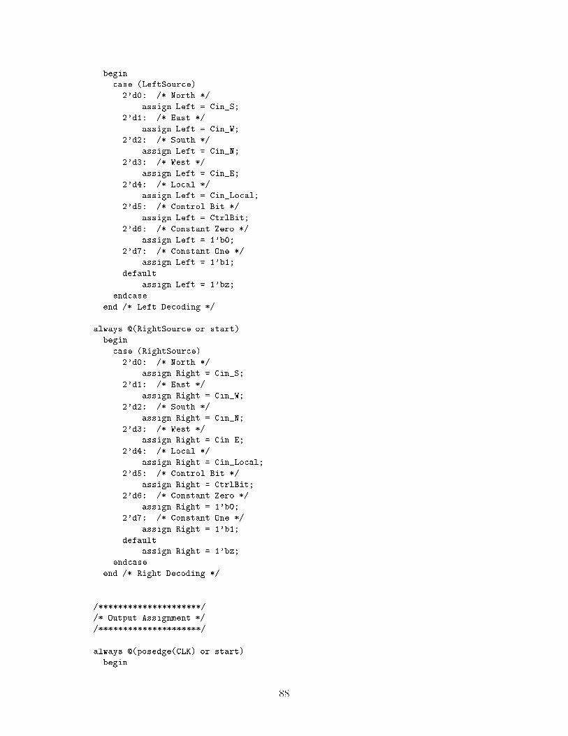
begincase (LeftSource)2'd0: /* North */assign Left = Cin_S;2'd1: /* East */assign Left = Cin_W;2'd2: /* South */assign Left = Cin_N;2'd3: /* West */assign Left = Cin_E;2'd4: /* Local */assign Left = Cin_Local;2'd5: /* Control Bit */assign Left = CtrlBit;2'd6: /* Constant Zero */assign Left = 1'b0;2'd7: /* Constant One */assign Left = 1'b1;defaultassign Left = 1'bz;endcaseend /* Left Decoding */always @(RightSource or start)begincase (RightSource)2'd0: /* North */assign Right = Cin_S;2'd1: /* East */assign Right = Cin_W;2'd2: /* South */assign Right = Cin_N;2'd3: /* West */assign Right = Cin_E;2'd4: /* Local */assign Right = Cin_Local;2'd5: /* Control Bit */assign Right = CtrlBit;2'd6: /* Constant Zero */assign Right = 1'b0;2'd7: /* Constant One */assign Right = 1'b1;defaultassign Right = 1'bz;endcaseend /* Right Decoding *//*********************//* Output Assignment *//*********************/always @(posedge(CLK) or start)begin 88

Left_reg = Left;Right_reg = Right;endSel2 #(1) LeftSel(Left, Left_reg, Cin_left, CarryPipeline, start);Sel2 #(1) RightSel(Right, Right_reg, Cin_right,(CarryPipeline || ((RightSource === 4'd4) &&(AddSig === 1'b1))),start);endmodule
89
/*******************************//* Specifications for Config.v *//*******************************//* The Config module contains two configuration memories, and the logic todeocde those memories into the actual configuration words (listed below).Also in this module are the constant configurations.This module does not handle the OR plane.Note that the high bit of ProgAdd selects between the two programmablecontexts for programming.The Hardwired Contexts:Ctx0: Write ContextL3_V1 : <WEmain (1 bit), 5'b0, WEconfig (1 bit), 1'b0>Fed into BOTH function ports.L3_V2 : <2'b0, RowAddress (3 bits), ColAddress (3 bits)>Decoded intro a control bit by C/R II, through FP1.L3_V3 : Memory Address (A port)L3_V4 : Data (B port)In this context, the L3_H lines would be driven with theirmatching L3_V line (ie: L3_H1 = L3_V1), on a one-cycle delay.On a real chip, these lines would be driven in at least one row,so that the north-side inputs (programming) are available to theother sides.Ctx1: Read ContextUses L3_V1 as the memory address, andL3_V2 as the main memory/config memory selection (Fm Port).L3_V3 is the output line.Row selection is performed by the perimeter L3 controllers.Inputs:Gctx : Global Context Select (2 bits)ProgAdd: Programming Address (8 bits)ProgDara: Programming Data (8 bits)PWE: Programming Write Enable (1 bit)PRE: Programming Read Enable (1 bit)CLK: Global Write Clock (1 bit)start : The model-specific initalization forces this module to re-read itsfiles.Outputs:MSB, LSB, CarryPipeline (1 bit each) : BFUcore configurationTS_Enable, MAdd1source, MAdd2source : BFUcore configurationRightSource, LeftSource (3 bits each) : BFUcore configuationFa_a, Fa_b (9 bits each) : ALU Function Port90

Fm_a, Fm_b (9 bits each) : MEM Function PortA_a, A_b (10 bits each) : A Address PortB_0, B_0 (10 bits each) : B Address PortN1_a, N1_b (10 bits each) : Network Port 1N2_a, N2_b (10 bits each) : Network Port 2FP1_a, FP1_b (9 bits each) : Floating Port 1FP2_a, FP2_b (9 bits each) : Floating Port 2L1_Enable (4 bits): Level-1 Driver EnablesL2_1_Enable (2 bits): Level-2 Driver 1 EnablesL2_2_Enable (2 bits): Level-2 Driver 2 EnablesL2_1 (2 bits): Level-2 Driver 1 SelectorL2_2 (2 bits): Level-2 Driver 2 SelectorL3_V4, L3_V3, L3_V2, L3_V1 (2 bits each): Level-3 Driver SelectorsL3_H4, L3_H3, L3_H2, L3_H1 (2 bits each): Level-3 Driver SelectorsTS_A, TS_B, TS_Fa, TS_Fm (4 bits each): Time-Switch Register ValuesTS_FP1, TS_FP2, TS_WE, TS_CR (4 bits each): Time-Switch Register ValuesTS_MAdd1, TS_MAdd2 : Time-Switch Register ValuesCRI_a, CRI_b (18 bits each) : Compare/Reduce I ConfigurationCRII (42 bits) : Compare/Reduce II ConfigurationCRsel_1, CRsel_2, CRsel_3, CRsel_4 (4 bits each): NOR Plane Input SelectorsCRIIsel (1 bit) : Compare/Reduce II Input SelectorCtrlBitsel (1 bit) : Control Bit Selector*//*****************//* Module Config *//*****************/module Config(start, Gctx, ProgAdd, ProgData, PWE, PRE, CLK,DataOut,LSB, MSB, RightSource, LeftSource, TS_Enable,MAdd1source, MAdd2source, CarryPipeline,Fa_a, Fa_b, Fm_a, Fm_b, A_a, A_b, B_a, B_b,N1_a, N1_b, N2_a, N2_b, FP1_a, FP1_b, FP2_a, FP2_b,L1_Enable, L2_1_Enable, L2_2_Enable,L2_1, L2_2,L3_V4, L3_V3, L3_V2, L3_V1,L3_H4, L3_H3, L3_H2, L3_H1,TS_A, TS_B, TS_Fa, TS_Fm, TS_FP1, TS_FP2, TS_WE, TS_CR,TS_MAdd1, TS_MAdd2, CRI_a, CRI_b, CRII,CRsel_1, CRsel_2, CRsel_3, CRsel_4, CRIIsel, CtrlBitsel);/**************/ 91

/* Parameters *//**************//* X and Y position of the BFU.These are used for the constant configuations */parameter X = 0;parameter Y = 0;/********************//* I/O Declarations *//********************/input [1:0] Gctx;input [7:0] ProgAdd, ProgData;input PWE, PRE, CLK, start;output [7:0] DataOut;reg [7:0] DataOut;output LSB, MSB, TS_Enable, MAdd1source, MAdd2source, CarryPipeline;output [2:0] RightSource, LeftSource;reg LSB, MSB, TS_Enable, MAdd1source, MAdd2source, CarryPipeline;reg [2:0] RightSource, LeftSource;output [8:0] Fa_a, Fa_b, Fm_a, Fm_b;reg [8:0] Fa_a, Fa_b, Fm_a, Fm_b;output [9:0] A_a, A_b, B_a, B_b;reg [9:0] A_a, A_b, B_a, B_b;output [9:0] N1_a, N1_b, N2_a, N2_b;reg [9:0] N1_a, N1_b, N2_a, N2_b;output [8:0] FP1_a, FP1_b, FP2_a, FP2_b;reg [8:0] FP1_a, FP1_b, FP2_a, FP2_b;output [3:0] L1_Enable;output [1:0] L2_1_Enable, L2_2_Enable;reg [3:0] L1_Enable;reg [1:0] L2_1_Enable, L2_2_Enable;output [1:0] L2_1, L2_2;output [1:0] L3_V4, L3_V3, L3_V2, L3_V1;output [1:0] L3_H4, L3_H3, L3_H2, L3_H1;reg [1:0] L2_1, L2_2;reg [1:0] L3_V4, L3_V3, L3_V2, L3_V1;reg [1:0] L3_H4, L3_H3, L3_H2, L3_H1;output [3:0] TS_A, TS_B, TS_Fa, TS_Fm, TS_FP1;output [3:0] TS_FP2, TS_WE, TS_CR, TS_MAdd1, TS_MAdd2;reg [3:0] TS_A, TS_B, TS_Fa, TS_Fm, TS_FP1;reg [3:0] TS_FP2, TS_WE, TS_CR, TS_MAdd1, TS_MAdd2;92

output [17:0] CRI_a, CRI_b;output [41:0] CRII;reg [17:0] CRI_a, CRI_b;reg [41:0] CRII;output [3:0] CRsel_1, CRsel_2, CRsel_3, CRsel_4;output CRIIsel, CtrlBitsel;reg [3:0] CRsel_1, CRsel_2, CRsel_3, CRsel_4;reg CRIIsel, CtrlBitsel;/*************************************//* Define the Configuration Memories *//*************************************/reg[7:0] Ctx2[45:0];reg[7:0] Ctx3[45:0];/**********************//* Handle Programming *//**********************/always @(posedge(CLK) && (PWE === 1'b1))beginif (ProgAdd[6] === 1'b0)beginif (ProgAdd[7] === 1'b0)Ctx2[ProgAdd[5:0]] = ProgData;elseCtx3[ProgAdd[5:0]] = ProgData;endend/******************//* Handle Reading *//******************/always @(posedge(CLK) && (PRE === 1'b1))beginif (ProgAdd[7] === 1'b0)DataOut = Ctx2[ProgAdd[5:0]];elseDataOut = Ctx3[ProgAdd[5:0]];end/**********************//* Temporary Register *//**********************//* Note that this are required because verilog does not supportbit-selects of memory elements */ 93

reg [7:0] TempReg;/**************************//* Handle Context Changes *//**************************/always @(start or Gctx or negedge(PWE))beginif (Gctx === 2'd0)beginMSB = 1'b0;LSB = 1'b0;RightSource = 3'd0;LeftSource = 3'd0;MAdd2source = 1'b0;MAdd1source = 1'b0;TS_Enable = 1'b0;CarryPipeline = 1'b0;Fa_a = {1'b0, 8'd0};Fa_b = {1'b1, 8'd21};Fm_a = {1'b0, 8'd0};Fm_b = {1'b1, 8'd21};A_a = {2'b11, 8'd23};A_b = {2'b11, 8'd23};B_a = {2'b11, 8'd24};B_b = {2'b11, 8'd24};N1_a = {2'b11, 8'd24};N1_b = {2'b11, 8'd24};N2_a = {2'b11, 8'd23};N2_b = {2'b11, 8'd23};FP1_a = {1'b1, 8'd22};FP1_b = {1'b1, 8'd22};FP2_a = {1'b0, 8'd21};FP2_b = {1'b0, 8'd21};L1_Enable = 4'b0000;L2_1 = 2'd0;L2_2 = 2'd0;L2_1_Enable = 2'b00;L2_2_Enable = 2'b00;L3_V1 = 2'd0;L3_V2 = 2'd0;L3_V3 = 2'd0;L3_V4 = 2'd0;L3_H1 = 2'd3; 94

L3_H2 = 2'd2;L3_H3 = 2'd1;L3_H4 = 2'd0;TS_A = 4'd0;TS_B = 4'd0;TS_Fa = 4'd0;TS_Fm = 4'd0;TS_FP1 = 4'd0;TS_FP2 = 4'd0;TS_CR = 4'd0;TS_WE = 4'd0;TS_MAdd1 = 4'd0;TS_MAdd2 = 4'd0;CRI_a = {2'd0,2'd0,2'd0,2'd0,2'd0,2'd0,2'd0,2'd0,2'd0};CRI_b = {2'd0,2'd0,2'd0,2'd0,2'd0,2'd0,2'd0,2'd0,2'd0};CRII = {2'd3, 2'd3,Num2CR(Y),Num2CR(X),2'd3,2'd3,2'd3,2'd3,2'd3,2'd3,2'd3,2'd3,2'd3,2'd3,2'd3,2'd3,2'd3};CRsel_1 = 4'd0;CRsel_2 = 4'd0;CRsel_3 = 4'd0;CRsel_4 = 4'd0;CtrlBitsel = 1'b0;CRIIsel = 1'b0;endif (Gctx === 2'd1)beginMSB = 1'b0;LSB = 1'b0;RightSource = 3'd0;LeftSource = 3'd0;MAdd2source = 1'b0;MAdd1source = 1'b0;TS_Enable = 1'b0;CarryPipeline = 1'b0;Fa_a = {1'b0, 4'b0000, 4'd12};Fa_b = {1'b0, 4'b0000, 4'd12};Fm_a = {1'b0, 8'd22};Fm_b = {1'b0, 8'd22};A_a = {2'b11, 8'd21};A_b = {2'b11, 8'd21};B_a = {2'b00, 8'd30};B_b = {2'b00, 8'd30};N1_a = {2'b11, 8'd0}; 95

N1_b = {2'b11, 8'd0};N2_a = {2'b00, 8'd30};N2_b = {2'b00, 8'd30};FP1_a = {1'b0, 8'd30};FP1_b = {1'b0, 8'd30};FP2_a = {1'b0, 8'd30};FP2_b = {1'b0, 8'd30};L1_Enable = 4'b0000;L2_1 = 2'd0;L2_2 = 2'd0;L2_1_Enable = 2'b00;L2_2_Enable = 2'b00;L3_V1 = 2'd0;L3_V2 = 2'd0;L3_V3 = 2'd0;L3_V4 = 2'd0;L3_H1 = 2'd0;L3_H2 = 2'd0;L3_H3 = 2'd0;L3_H4 = 2'd0;TS_A = 4'd0;TS_B = 4'd0;TS_Fa = 4'd0;TS_Fm = 4'd0;TS_FP1 = 4'd0;TS_FP2 = 4'd0;TS_CR = 4'd0;TS_WE = 4'd0;TS_MAdd1 = 4'd0;TS_MAdd2 = 4'd0;CRI_a = {2'd0,2'd0,2'd0,2'd0,2'd0,2'd0,2'd0,2'd0,2'd0};CRI_b = {2'd0,2'd0,2'd0,2'd0,2'd0,2'd0,2'd0,2'd0,2'd0};CRII = {2'd3,2'd3,2'd3,2'd3,2'd3,2'd3,2'd3,2'd3,2'd3,2'd3,2'd3,2'd3,2'd3,2'd3,2'd3,2'd3,2'd3,2'd3,2'd3,2'd3,2'd3};CRsel_1 = 4'd0;CRsel_2 = 4'd0;CRsel_3 = 4'd0;CRsel_4 = 4'd0;CtrlBitsel = 1'b0;CRIIsel = 1'b0;endif (Gctx === 2'd2) 96
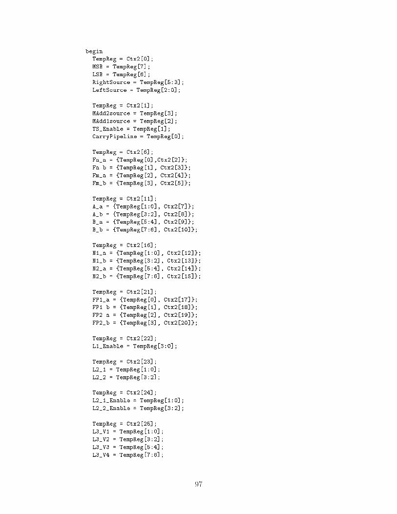
beginTempReg = Ctx2[0];MSB = TempReg[7];LSB = TempReg[6];RightSource = TempReg[5:3];LeftSource = TempReg[2:0];TempReg = Ctx2[1];MAdd2source = TempReg[3];MAdd1source = TempReg[2];TS_Enable = TempReg[1];CarryPipeline = TempReg[0];TempReg = Ctx2[6];Fa_a = {TempReg[0],Ctx2[2]};Fa_b = {TempReg[1], Ctx2[3]};Fm_a = {TempReg[2], Ctx2[4]};Fm_b = {TempReg[3], Ctx2[5]};TempReg = Ctx2[11];A_a = {TempReg[1:0], Ctx2[7]};A_b = {TempReg[3:2], Ctx2[8]};B_a = {TempReg[5:4], Ctx2[9]};B_b = {TempReg[7:6], Ctx2[10]};TempReg = Ctx2[16];N1_a = {TempReg[1:0], Ctx2[12]};N1_b = {TempReg[3:2], Ctx2[13]};N2_a = {TempReg[5:4], Ctx2[14]};N2_b = {TempReg[7:6], Ctx2[15]};TempReg = Ctx2[21];FP1_a = {TempReg[0], Ctx2[17]};FP1_b = {TempReg[1], Ctx2[18]};FP2_a = {TempReg[2], Ctx2[19]};FP2_b = {TempReg[3], Ctx2[20]};TempReg = Ctx2[22];L1_Enable = TempReg[3:0];TempReg = Ctx2[23];L2_1 = TempReg[1:0];L2_2 = TempReg[3:2];TempReg = Ctx2[24];L2_1_Enable = TempReg[1:0];L2_2_Enable = TempReg[3:2];TempReg = Ctx2[25];L3_V1 = TempReg[1:0];L3_V2 = TempReg[3:2];L3_V3 = TempReg[5:4];L3_V4 = TempReg[7:6]; 97
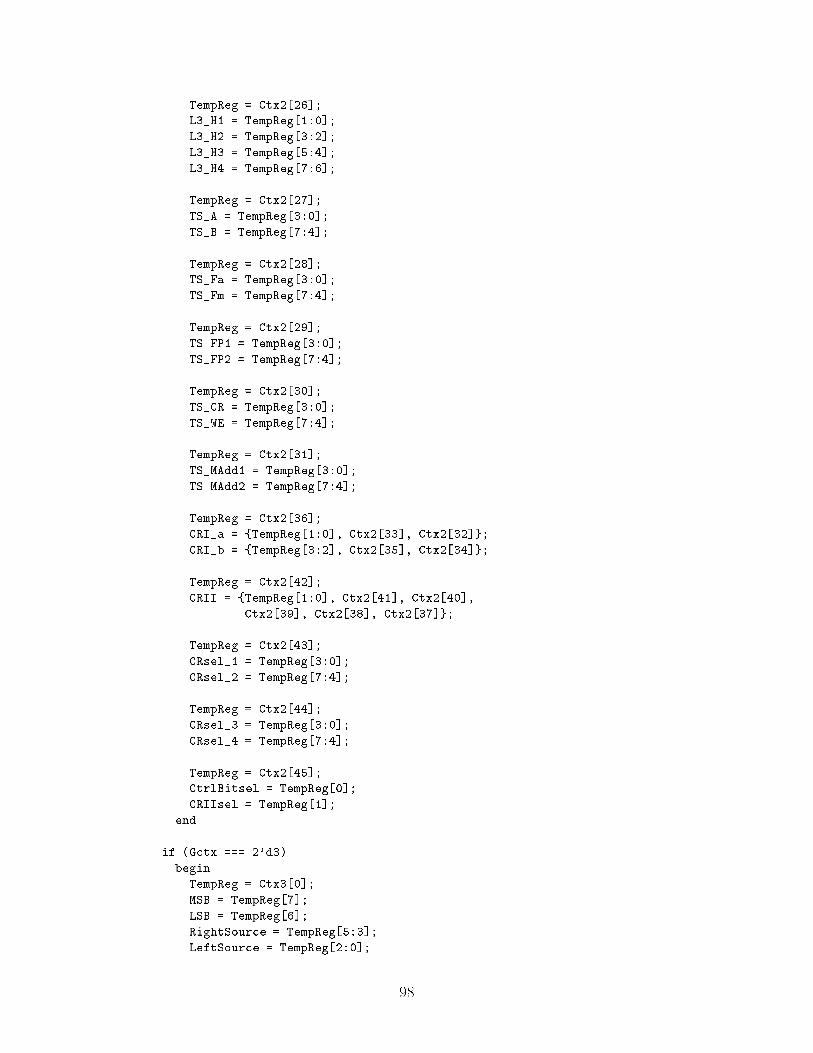
TempReg = Ctx2[26];L3_H1 = TempReg[1:0];L3_H2 = TempReg[3:2];L3_H3 = TempReg[5:4];L3_H4 = TempReg[7:6];TempReg = Ctx2[27];TS_A = TempReg[3:0];TS_B = TempReg[7:4];TempReg = Ctx2[28];TS_Fa = TempReg[3:0];TS_Fm = TempReg[7:4];TempReg = Ctx2[29];TS_FP1 = TempReg[3:0];TS_FP2 = TempReg[7:4];TempReg = Ctx2[30];TS_CR = TempReg[3:0];TS_WE = TempReg[7:4];TempReg = Ctx2[31];TS_MAdd1 = TempReg[3:0];TS_MAdd2 = TempReg[7:4];TempReg = Ctx2[36];CRI_a = {TempReg[1:0], Ctx2[33], Ctx2[32]};CRI_b = {TempReg[3:2], Ctx2[35], Ctx2[34]};TempReg = Ctx2[42];CRII = {TempReg[1:0], Ctx2[41], Ctx2[40],Ctx2[39], Ctx2[38], Ctx2[37]};TempReg = Ctx2[43];CRsel_1 = TempReg[3:0];CRsel_2 = TempReg[7:4];TempReg = Ctx2[44];CRsel_3 = TempReg[3:0];CRsel_4 = TempReg[7:4];TempReg = Ctx2[45];CtrlBitsel = TempReg[0];CRIIsel = TempReg[1];endif (Gctx === 2'd3)beginTempReg = Ctx3[0];MSB = TempReg[7];LSB = TempReg[6];RightSource = TempReg[5:3];LeftSource = TempReg[2:0]; 98
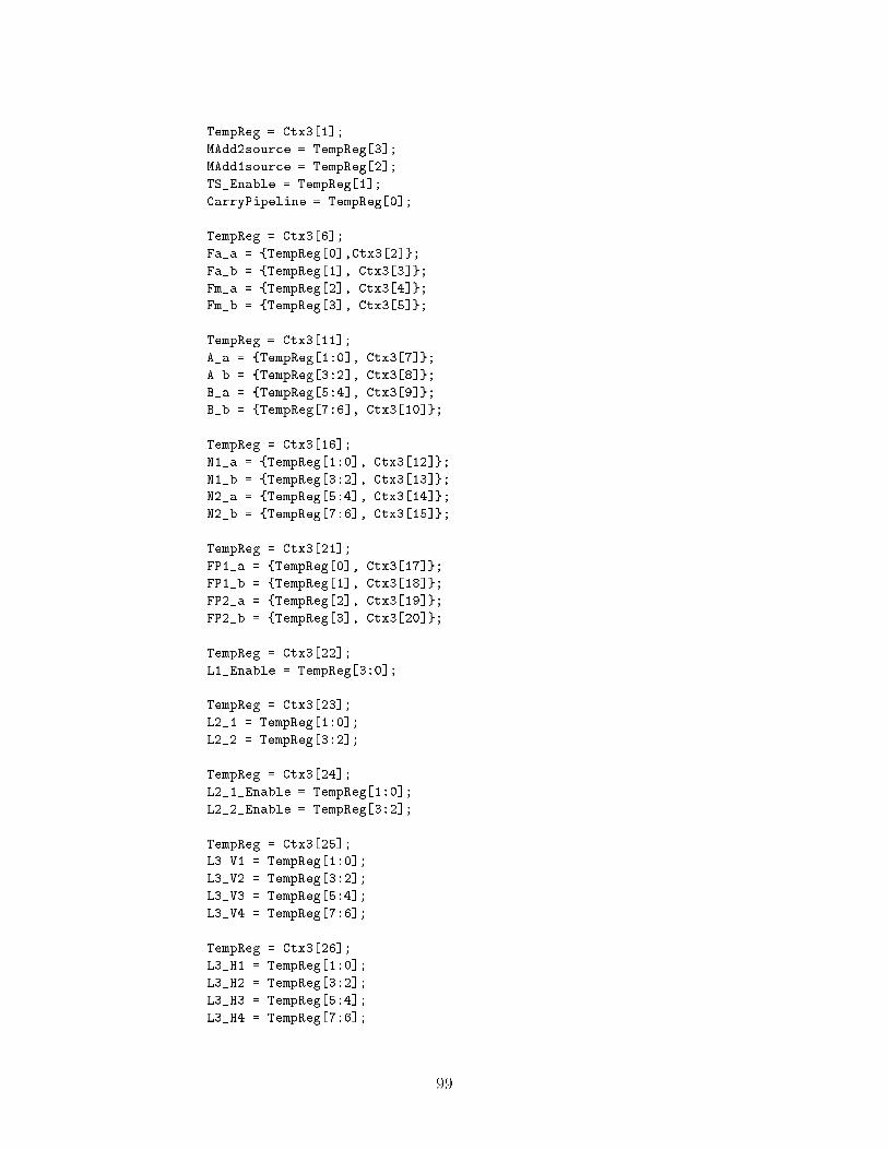
TempReg = Ctx3[1];MAdd2source = TempReg[3];MAdd1source = TempReg[2];TS_Enable = TempReg[1];CarryPipeline = TempReg[0];TempReg = Ctx3[6];Fa_a = {TempReg[0],Ctx3[2]};Fa_b = {TempReg[1], Ctx3[3]};Fm_a = {TempReg[2], Ctx3[4]};Fm_b = {TempReg[3], Ctx3[5]};TempReg = Ctx3[11];A_a = {TempReg[1:0], Ctx3[7]};A_b = {TempReg[3:2], Ctx3[8]};B_a = {TempReg[5:4], Ctx3[9]};B_b = {TempReg[7:6], Ctx3[10]};TempReg = Ctx3[16];N1_a = {TempReg[1:0], Ctx3[12]};N1_b = {TempReg[3:2], Ctx3[13]};N2_a = {TempReg[5:4], Ctx3[14]};N2_b = {TempReg[7:6], Ctx3[15]};TempReg = Ctx3[21];FP1_a = {TempReg[0], Ctx3[17]};FP1_b = {TempReg[1], Ctx3[18]};FP2_a = {TempReg[2], Ctx3[19]};FP2_b = {TempReg[3], Ctx3[20]};TempReg = Ctx3[22];L1_Enable = TempReg[3:0];TempReg = Ctx3[23];L2_1 = TempReg[1:0];L2_2 = TempReg[3:2];TempReg = Ctx3[24];L2_1_Enable = TempReg[1:0];L2_2_Enable = TempReg[3:2];TempReg = Ctx3[25];L3_V1 = TempReg[1:0];L3_V2 = TempReg[3:2];L3_V3 = TempReg[5:4];L3_V4 = TempReg[7:6];TempReg = Ctx3[26];L3_H1 = TempReg[1:0];L3_H2 = TempReg[3:2];L3_H3 = TempReg[5:4];L3_H4 = TempReg[7:6]; 99

TempReg = Ctx3[27];TS_A = TempReg[3:0];TS_B = TempReg[7:4];TempReg = Ctx3[28];TS_Fa = TempReg[3:0];TS_Fm = TempReg[7:4];TempReg = Ctx3[29];TS_FP1 = TempReg[3:0];TS_FP2 = TempReg[7:4];TempReg = Ctx3[30];TS_CR = TempReg[3:0];TS_WE = TempReg[7:4];TempReg = Ctx3[31];TS_MAdd1 = TempReg[3:0];TS_MAdd2 = TempReg[7:4];TempReg = Ctx3[36];CRI_a = {TempReg[1:0], Ctx3[33], Ctx3[32]};CRI_b = {TempReg[3:2], Ctx3[35], Ctx3[34]};TempReg = Ctx3[42];CRII = {TempReg[1:0], Ctx3[41], Ctx3[40],Ctx3[39], Ctx3[38], Ctx3[37]};TempReg = Ctx3[43];CRsel_1 = TempReg[3:0];CRsel_2 = TempReg[7:4];TempReg = Ctx3[44];CRsel_3 = TempReg[3:0];CRsel_4 = TempReg[7:4];TempReg = Ctx3[45];CtrlBitsel = TempReg[0];CRIIsel = TempReg[1];endend /* Context Changes *//********************************//* Number to CRconfig Converter *//********************************/function [5:0] Num2CR;input [2:0] Value;reg [1:0] Out[2:0];integer i;beginfor (i=0;i<3;i=i+1)beginif (Value[i] == 1'b0) 100

Out[i]=2'b01;elseOut[i]=2'b10;endNum2CR = {Out[2],Out[1],Out[0]};endendfunctionendmodule
101

/********************************//* Specifications for Control.v *//********************************//* Control.v is an assembly of most of the control logic in a BFU cell. Itincludes everything except Comp/Reduce I.This module takes in all the parameters of the NORplane as well.The inputs to Control are:CRin : The 13 neighborhood Compare/Reduce values.FP1 : The output of Floating Port 1.FP2 : The output of Floating Port 2.CLK : A clock.start : The standard simulator reset.Gctx : The global context selection.ProgAdd : Programming Address (OR plane)ProgData : Programming Data (OR plane)PWE : Programming WE (OR plane)PRE : Programming RE (OR plane)CRIIconfig : The configuration for Comp/Reduce II.CRIIsel : The input selector for Comp/Reduce II.CRsel1, CRsel2, CRsel3, CRsel4 : Selector configurations for the NOR array.CrtlBitsel : The selector for the control bit.TSenable : Enable for Time-Switch Registers.TScycle : Incoming Time-Switch Cycle.TS_CRconf, TS_FP1conf, TS_FP2conf : Configuation for Time-Switch Registers.The outputs of Control are:CtrlBit : The Control BitCtrlByte : The Control ByteOR_Config : The read-out data from the OR plane configuration*//*****************//* Include Files *//*****************/`include "ORplane.v"`ifdef selector_defined`else`include "Selector.v"`endif`ifdef TSregister_defined`else`include "TSregister.v" 102

`endif`ifdef CompReduce_defined`else`include "CompReduce.v"`endif/******************//* Module Control *//******************/module Control (CRin, FP1, FP2, CtrlBit, CtrlByte, CLK, Gctx,ProgAdd, ProgData, PWE, PRE, start,OR_Config,CRIIconfig, CRIIsel, CRsel1, CRsel2, CRsel3, CRsel4,CtrlBitsel, TSenable, TScycle, TS_CRconf, TS_FP1conf,TS_FP2conf);/********************//* I/O Declarations *//********************/input [12:0] CRin;input [7:0] FP1, FP2;input CLK, start;input [1:0] Gctx;input [7:0] ProgAdd, ProgData;input PWE, PRE;input [41:0] CRIIconfig;input CRIIsel, CtrlBitsel;input [3:0] CRsel1, CRsel2, CRsel3, CRsel4;input TSenable;input [3:0] TScycle, TS_CRconf, TS_FP1conf, TS_FP2conf;output [7:0] OR_Config;output [7:0] CtrlByte;output CtrlBit;/******************//* Internal Wires *//******************//* The registered inputs */wire [12:0] CRin_reg;wire [7:0] FP1_reg, FP2_reg;/* The input to C/R II */ 103

wire [7:0] CRIIin;/* The 4 selected CR for the OR array */wire CR_OR1, CR_OR2, CR_OR3, CR_OR4;/* The Bit outputs of the OR and CRII */wire CRIIout, ORout;/*************************//* Time-Switch Registers *//*************************/TSregister #(13) TS_CR(CRin, TScycle, CRin_reg, TSenable, TS_CRconf,CLK, start);TSregister #(8) TS_FP1(FP1, TScycle, FP1_reg, TSenable, TS_FP1conf,CLK, start);TSregister #(8) TS_FP2(FP2, TScycle, FP2_reg, TSenable, TS_FP2conf,CLK, start);/*******************//* Input Selectors *//*******************/Sel2 #(8) CRIIin_sel(FP1_reg, FP2_reg, CRIIin, CRIIsel, start);Sel16 CR_OR1_sel({4'd0,CRin_reg}, CR_OR1, CRsel1, start);Sel16 CR_OR2_sel({4'd0,CRin_reg}, CR_OR2, CRsel2, start);Sel16 CR_OR3_sel({4'd0,CRin_reg}, CR_OR3, CRsel3, start);Sel16 CR_OR4_sel({4'd0,CRin_reg}, CR_OR4, CRsel4, start);/****************//* Main Modules *//****************/CompReduce #(21) CRII({CRIIin, CRin_reg}, CRIIconfig, CRIIout, start);ORplane ORarray({CR_OR1, CR_OR2, CR_OR3, CR_OR4, FP2_reg, FP1_reg},Gctx, CLK, {ORout, CtrlByte}, ProgAdd, ProgData,PWE, PRE, OR_Config, start);/*******************//* Output Selector *//*******************/Sel2 #(1) CtrlBit_sel(CRIIout, ORout, CtrlBit, CtrlBitsel, start);endmodule 104
/*********************************//* Specifications for NORplane.v *//*********************************//* ORplane is the model of the MATRIX control logic OR plane. The inputsto this module are the the 20 main inputs to the OR plane. Internally,they will each be inverted, and then both polarities are fed into theOR plane itself. The configuration of the OR plane is read of a file,and is senstive to the global context changes.The inputs of ORplane:Data : The 20-bit wide input vector.Gctx : The two bit global context.CLK : The global CLK.start : The standard simulation reset.ProgAdd : Programming AddressProgData : Programming DataPWE : Programming WEPRE : Programming REThe outputs of ORplane is the 9-bit output vector andOR_Config, the output of the configuration memories during a read.*//*****************//* Include Files *//*****************/`ifdef selector_defined`else`include "Selector.v"`endif/*******************//* Module ORplane *//*******************/module ORplane(Data, Gctx, CLK, Out, ProgAdd, ProgData, PWE, PRE,OR_Config, start);/********************//* I/O Declarations *//********************/input [19:0] Data;input [1:0] Gctx;input [7:0] ProgAdd, ProgData;input CLK, PWE, PRE, start;output [7:0] OR_Config;reg [7:0] OR_Config; 105

output [8:0] Out;/********************//* Output Registers *//********************/reg [8:0] OR_out; /* Output of the OR plane *//***********************************//* Define the Configuration Memory *//***********************************/reg[7:0] ReadMem[44:0]; /* This accepts data */reg[39:0] ORMem[8:0]; /* This is basis for the OR array *//****************//* Handle Reads *//****************/always @(posedge(CLK) && (PRE === 1'b1))beginOR_Config = ReadMem[ProgAdd[5:0]];end/*******************//* Program ReadMem *//*******************/always @(posedge(CLK) && (PWE === 1'b1))beginif (ProgAdd[6] === 1'b1)beginReadMem[ProgAdd[5:0]] = ProgData;/********************//* Setup the ORMem *//********************/ORMem[0] = {ReadMem[4],ReadMem[3],ReadMem[2],ReadMem[1],ReadMem[0]};ORMem[1] = {ReadMem[9],ReadMem[8],ReadMem[7],ReadMem[6],ReadMem[5]};ORMem[2] = {ReadMem[14],ReadMem[13],ReadMem[12],ReadMem[11],ReadMem[10]};ORMem[3] = {ReadMem[19],ReadMem[18],ReadMem[17],ReadMem[16],ReadMem[15]};ORMem[4] = {ReadMem[24],ReadMem[23],ReadMem[22],ReadMem[21],ReadMem[20]};ORMem[5] = {ReadMem[29],ReadMem[28],ReadMem[27],106

ReadMem[26],ReadMem[25]};ORMem[6] = {ReadMem[34],ReadMem[33],ReadMem[32],ReadMem[31],ReadMem[30]};ORMem[7] = {ReadMem[39],ReadMem[38],ReadMem[37],ReadMem[36],ReadMem[35]};ORMem[8] = {ReadMem[44],ReadMem[43],ReadMem[42],ReadMem[41],ReadMem[40]};endend/***********************//* Define the OR Plane *//***********************/initialbegin$async$or$array(ORMem,{~Data[19],Data[19],~Data[18],Data[18],~Data[17],Data[17],~Data[16],Data[16],~Data[15],Data[15],~Data[14],Data[14],~Data[13],Data[13],~Data[12],Data[12],~Data[11],Data[11],~Data[10],Data[10],~Data[9],Data[9],~Data[8],Data[8],~Data[7],Data[7],~Data[6],Data[6],~Data[5],Data[5],~Data[4],Data[4],~Data[3],Data[3],~Data[2],Data[2],~Data[1],Data[1],~Data[0],Data[0]},{OR_out[8],OR_out[7],OR_out[6],OR_out[5],OR_out[4],OR_out[3],OR_out[2],OR_out[1],OR_out[0]});end/*******************//* Output Selector *//*******************/Sel2 #(9) OutSel(9'b0,OR_out,Out,Gctx[1],start);endmodule107

/* The following is necessary because this file may be read from many inlcudestatements and should be ignored on all but the first */`define CompReduce_defined/***********************************//* Specifications for CompReduce.v *//***********************************//* CompReduce module models the Comparison/Reduction operation of the MATRIXcontrol logic. It takes in a (parameterized-length) input word, andcompares it to a configuration word, which can include "don't care" and"fail" bits. If all bits pass their test, the output of the module ishigh, otherwise the output is low. See TN130 for more details includingthe actual bit-encoding.The inputs to CompReduce are:Data : The Data input.Config : The configuration word. Twice as large as the Data input.start : The standard simulator reset.The output is Match.There are actually two modules in this file. The basic CompReduce isdescribed above. The second is CompReduceI, which adds a double-contextconfiguration word to the basic CompReduce.*//*****************//* Include Files *//*****************/`ifdef selector_defined`else`include "Selector.v"`endif/*********************//* Module CompReduce *//*********************/module CompReduce (Data, Config, Match, start);/* Define the size of the Data and Config words */parameter size = 1;input [size-1:0] Data;input [(2*size)-1:0] Config;input start;output Match; 108

reg Match;/**********************//* Internal Variables *//**********************/integer i;/***************//* Begin Model *//***************/always @(Data or Config or start)begin/* Initialize Match to true, then update with comparisons to each bit */Match = 1'b1;for (i=0; i<size; i=i+1)beginif (Data[i]===1'b0)Match = Match && Config[i*2];elseMatch = Match && Config[(i*2)+1];endendendmodule/**********************//* Module CompReduceI *//**********************/module CompReduceI (Data, ConfigA, ConfigB, Ctrl, Match, start);/* Define the size of the Data and Config words */parameter size=1;input [size-1:0] Data;input [(2*size)-1:0] ConfigA, ConfigB;input Ctrl, start;output Match;/*****************//* Internal Wire *//*****************/wire [(2*size)-1:0] Config; 109

/**************************//* Configuration Selector *//**************************/Sel2 #(size*2) CtxSel(ConfigA, ConfigB, Config, Ctrl, start);/*************************//* The CompReduce Module *//*************************/CompReduce #(size) CR(Data, Config, Match, start);endmodule
110
/******************************//* Specifications for Fport.v *//******************************//* An Fport is the switch used to feed data to the BFU function and floatingports. It consists of a NetSwitch, and a few selectors which are used toconfigure the port, based on incoming configuration data. No registerappears at this level of the simuluation. See TN130 for a block diagramof the port's operation.The inputs to an Fport (in addition to the main network inputs)Config_a, Config_b : The configuration Contexts.Each of these is a 9-bit value.Ctrl : Local Control BitAnd, of cource:Input start is a model-specific initialization input, used to force themodule to evaluate its inputs.*//*****************//* Include Files *//*****************/`ifdef selector_defined`else`include "Selector.v"`endif`ifdef netswitch_defined`else`include "NetSwitch.v"`endif/****************//* Module Fport *//****************/module Fport(Local, L1_N1, L1_N2, L1_NE, L1_E1, L1_E2, L1_SE, L1_S1, L1_S2,L1_SW, L1_W1, L1_W2, L1_NW,L2_N1, L2_N2, L2_E1, L2_E2, L2_S1, L2_S2, L2_W1, L2_W2,L3_V1, L3_V2, L3_V3, L3_V4, L3_H1, L3_H2, L3_H3, L3_H4, CByte,Config_a, Config_b, Ctrl, Out, start);input [7:0] Local, L1_N1, L1_N2, L1_NE, L1_E1, L1_E2, L1_SE, L1_S1, L1_S2;input [7:0] L1_SW, L1_W1, L1_W2, L1_NW;input [7:0] L2_N1, L2_N2, L2_E1, L2_E2, L2_S1, L2_S2, L2_W1, L2_W2;input [7:0] L3_V1, L3_V2, L3_V3, L3_V4, L3_H1, L3_H2, L3_H3, L3_H4, CByte;111

input [8:0] Config_a, Config_b;input Ctrl;output [7:0] Out;input start;/******************//* Internal Wires *//******************/wire [8:0] Config; /* Final configuration word *//******************************//* Delacare the major modules *//******************************/NetSwitch switch(Local, L1_N1, L1_N2, L1_NE, L1_E1, L1_E2, L1_SE, L1_S1,L1_S2, L1_SW, L1_W1, L1_W2, L1_NW,L2_N1, L2_N2, L2_E1, L2_E2, L2_S1, L2_S2, L2_W1, L2_W2,L3_V1, L3_V2, L3_V3, L3_V4, L3_H1, L3_H2, L3_H3, L3_H4,CByte,Config[4:0], Config[7:0], Config[8], Out, start);Sel2 #(9) Ctx_Sel(Config_a, Config_b, Config, Ctrl, start);endmodule
112

/*******************************//* Specifications for NAport.v *//*******************************//* An NAport is the switch used to feed data to the BFU L2 and L3 networkdrivers and address ports. It consists of a NetSwitch, and a fewselectors which are used to to configure the port, based on incomingconfiguration data. No registers are included at this level ofsimulation. See TN130 for a block diagram of the port's operation.The inputs to an NAport (in addition to the main network inputs)Config_a, Config_b : The configuration Contexts.Each of these is a 10-bit value.FPout : Alternate SourceSel (5 bits)Ctrl : Local Control BitAnd, of cource:Input start is a model-specific initialization input, used to force themodule to evaluate its inputs.*//*****************//* Include Files *//*****************/`ifdef selector_defined`else`include "Selector.v"`endif`ifdef netswitch_defined`else`include "NetSwitch.v"`endif/*****************//* Module NAport *//*****************/module NAport(Local, L1_N1, L1_N2, L1_NE, L1_E1, L1_E2, L1_SE, L1_S1, L1_S2,L1_SW, L1_W1, L1_W2, L1_NW,L2_N1, L2_N2, L2_E1, L2_E2, L2_S1, L2_S2, L2_W1, L2_W2,L3_V1, L3_V2, L3_V3, L3_V4, L3_H1, L3_H2, L3_H3, L3_H4, CByte,Config_a, Config_b, FPout, Ctrl, Out, start);input [7:0] Local, L1_N1, L1_N2, L1_NE, L1_E1, L1_E2, L1_SE, L1_S1, L1_S2;input [7:0] L1_SW, L1_W1, L1_W2, L1_NW;input [7:0] L2_N1, L2_N2, L2_E1, L2_E2, L2_S1, L2_S2, L2_W1, L2_W2;input [7:0] L3_V1, L3_V2, L3_V3, L3_V4, L3_H1, L3_H2, L3_H3, L3_H4, CByte;113

input [9:0] Config_a, Config_b;input [7:0] FPout;input Ctrl;output [7:0] Out;input start;/******************//* Internal Wires *//******************/wire [4:0] SourceSel; /* Final Source Selector */wire [9:0] Config; /* Final configuration word *//******************************//* Delacare the major modules *//******************************/NetSwitch switch(Local, L1_N1, L1_N2, L1_NE, L1_E1, L1_E2, L1_SE, L1_S1,L1_S2, L1_SW, L1_W1, L1_W2, L1_NW,L2_N1, L2_N2, L2_E1, L2_E2, L2_S1, L2_S2, L2_W1, L2_W2,L3_V1, L3_V2, L3_V3, L3_V4, L3_H1, L3_H2, L3_H3, L3_H4,CByte,SourceSel, Config[7:0], Config[8], Out, start);Sel2 #(10) Ctx_sel(Config_a, Config_b, Config, Ctrl, start);Sel2 #(5) source_sel(Config[4:0], FPout[4:0], SourceSel, ~Config[9], start);endmodule114
/**********************************//* Specifications for L1drivers.v *//**********************************//* L1drivers represent the drivers that enable the BFU's outputLevel 1 lines. When enabled, the drive the BFU output along theappropriate wires. When disabled, they drive the lines to ground.The inputs to L1drivers are:BFUout : The output of the BFUcoreEnables : The 4 enable bits in the order N,E,S,W (msb->lsb)start : The standard simualtion reset signalThe outputs of L1drivers:L1_N, L1_E, L1_S, L1_W : The appropriate Level 1 output lines.*//********************//* Module L1drivers *//********************/module L1drivers (BFUout[7:0], Enables[3:0], start,L1_N[7:0], L1_E[7:0], L1_S[7:0], L1_W[7:0]);input [7:0] BFUout;input [3:0] Enables;input start;output [7:0] L1_N, L1_E, L1_S, L1_W;reg [7:0] L1_N, L1_E, L1_S, L1_W;/* Handle the Enables */always @(Enables or start)beginif (Enables[3]===1'b1)assign L1_N = BFUout;elseassign L1_N = 8'd0;if (Enables[2]===1'b1)assign L1_E = BFUout;elseassign L1_E = 8'd0;if (Enables[1]===1'b1)assign L1_S = BFUout;elseassign L1_S = 8'd0; 115

if (Enables[0]===1'b1)assign L1_W = BFUout;elseassign L1_W = 8'd0;endendmodule
116

/*********************************//* Specifications for L2driver.v *//*********************************//* An L2driver drives the Level-2 network lines. When enabled it drives oneof its input onto its output. When disabled, it drives a zero.The driver also includes an optional register.The inputs to L2driver are:N1out, N2out, FP1out, FP2out : The incoming signals that can be driven.DRsel_A : Two-bit configuration word for the input selector.Enable : A two-bit word containing <driver enable, register enable>CLK : A clockstart : The standard simulator reset signalThe output of L2driver is Out, the final output of the driver.*//*****************//* Include Files *//*****************/`ifdef selector_defined`else`include "Selector.v"`endif/*******************//* Module L2driver *//*******************/module L2driver (N1out, N2out, FP1out, FP2out, Out, DRsel,Enable, CLK, start);input [7:0] N1out, N2out, FP1out, FP2out;input [1:0] DRsel, Enable;input CLK, start;output [7:0] Out;reg [7:0] Out;/********************************//* Internal Registers and Wires *//********************************/wire [7:0] data_A, data_B; /* Intermediate selector data */wire [7:0] SelData; /* The selected data */wire [7:0] FinalData; /* The final, selected and registered data */117
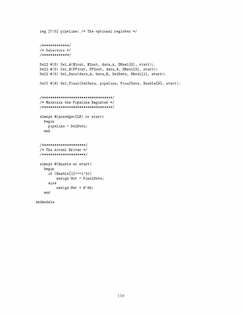
reg [7:0] pipeline; /* The optional register *//*************//* Selectors *//*************/Sel2 #(8) Sel_A(N1out, N2out, data_A, DRsel[0], start);Sel2 #(8) Sel_B(FP1out, FP2out, data_B, DRsel[0], start);Sel2 #(8) Sel_Data(data_A, data_B, SelData, DRsel[1], start);Sel2 #(8) Sel_Final(SelData, pipeline, FinalData, Enable[0], start);/**********************************//* Maintain the Pipeline Register *//**********************************/always @(posedge(CLK) or start)beginpipeline = SelData;end/*********************//* The Actual Driver *//*********************/always @(Enable or start)beginif (Enable[1]===1'b1)assign Out = FinalData;elseassign Out = 8'd0;endendmodule118

/*********************************//* Specifications for L3decode.v *//*********************************//* L3decode decodes the incoming Level-3 Network enable lines and outputsthe actual enables for the L3drivers.Parameters: (X,Y) BFU addressInputs:L3_V1en : Level-3 Enable, Vertical-1 Line. (4 bits)L3_V2en : Level-3 Enable, Vertical-2 Line. (4 bits)L3_V3en : Level-3 Enable, Vertical-3 Line. (4 bits)L3_V4en : Level-3 Enable, Vertical-4 Line. (4 bits)L3_H1en : Level-3 Enable, Horizontal-1 Line. (4 bits)L3_H2en : Level-3 Enable, Horizontal-2 Line. (4 bits)L3_H3en : Level-3 Enable, Horizontal-3 Line. (4 bits)L3_H4en : Level-3 Enable, Horizontal-4 Line. (4 bits)start : a model-specific initialization input, used to force themodule to evaluate its inputs.Ouputs: (one bit each)V1en : Enable L3_V1.V2en : Enable L3_V2.V3en : Enable L3_V3.V4en : Enable L3_V4.H1en : Enable L3_H1.H2en : Enable L3_H2.H3en : Enable L3_H3.H4en : Enable L3_H4.*//*******************//* Module L3decode *//*******************/module L3decode(L3_V1en, L3_V2en, L3_V3en, L3_V4en,L3_H1en, L3_H2en, L3_H3en, L3_H4en,V1en, V2en, V3en, V4en, H1en, H2en, H3en, H4en,start);/* Default Parameters */parameter X=0;parameter Y=0;/* I/O specifications */input [3:0] L3_V1en, L3_V2en, L3_V3en, L3_V4en;119

input [3:0] L3_H1en, L3_H2en, L3_H3en, L3_H4en;input start;output V1en, V2en, V3en, V4en, H1en, H2en, H3en, H4en;reg V1en, V2en, V3en, V4en, H1en, H2en, H3en, H4en;/******************//* Begin Decoding *//******************/always @(start or L3_V1en) /* Vertical 1 */beginif (L3_V1en===Y)V1en = 1'b1;elseV1en = 1'b0;endalways @(start or L3_V2en) /* Vertical 2 */beginif (L3_V2en===Y)V2en = 1'b1;elseV2en = 1'b0;endalways @(start or L3_V3en) /* Vertical 3 */beginif (L3_V3en===Y)V3en = 1'b1;elseV3en = 1'b0;endalways @(start or L3_V4en) /* Vertical 4 */beginif (L3_V4en===Y)V4en = 1'b1;elseV4en = 1'b0;endalways @(start or L3_H1en) /* Horizontal 1 */beginif (L3_H1en===X)H1en = 1'b1;elseH1en = 1'b0;endalways @(start or L3_H2en) /* Horizontal 2 */begin 120

if (L3_H2en===X)H2en = 1'b1;elseH2en = 1'b0;endalways @(start or L3_H3en) /* Horizontal 3 */beginif (L3_H3en===X)H3en = 1'b1;elseH3en = 1'b0;endalways @(start or L3_H4en) /* Horizontal 4 */beginif (L3_H4en===X)H4en = 1'b1;elseH4en = 1'b0;endendmodule
121

/*********************************//* Specifications for L3driver.v *//*********************************//* An L3driver drives the Level-3 network lines. It is a true tristatedriver. The driver also includes a register.The inputs to L2driver are:N1out, N2out, FP1out, FP2out : The incoming signals that can be driven.DRsel : Two-bit configuration words for the input selector.Enable : The one-bit driver enableCLK : A clockstart : The standard simulator reset signalThe output of L3driver is Out, the final output of the driver.*//*****************//* Include Files *//*****************/`ifdef selector_defined`else`include "Selector.v"`endif`ifdef trireg_defined`else`include "Trireg.v"`endif/*******************//* Module L3driver *//*******************/module L3driver (N1out, N2out, FP1out, FP2out, Out, DRsel,Enable, CLK, start);input [7:0] N1out, N2out, FP1out, FP2out;input [1:0] DRsel;input Enable;input CLK, start;output [7:0] Out;/********************************//* Internal Registers and Wires *//********************************/ 122

wire [7:0] data_A, data_B; /* Intermediate selector data */wire [7:0] SelData; /* The selected data *//*************//* Selectors *//*************/Sel2 #(8) Sel_A(N1out, N2out, data_A, DRsel[0], start);Sel2 #(8) Sel_B(FP1out, FP2out, data_B, DRsel[0], start);Sel2 #(8) Sel_Data(data_A, data_B, SelData, DRsel[1], start);/*******************//* Tristate Driver *//*******************/Trireg #(8) Driver(SelData, Enable, CLK, start, Out);endmodule
123

/*****************************//* Specifications for MAdd.v *//*****************************//* MAdd is the decoder for the Multiplier-Add inputs to a BFU. See TN130 forcomplete description of this part of MATRIX.Inputs to MAdd:HW1, HW2 : Hardwired input for MAdd1 and MAdd2. For the current revisionthese are assume to be L1_N1, and L1_NW, respectively.FP1, FP2 : Outputs of the Floating Port.Source1, Source2 : Source selector configuration.TSenable : Enable Time-SwitchingTScycle : Current Time-Switch CycleTS_MAdd1, TS_MAdd2 : Time-Switch Configutation.CLK : A clockstart : The simulator reset.Outputs of MAdd:MAdd1, MAdd2 : The final MAdd values.*//*****************//* Include Files *//*****************/`ifdef selector_defined`else`include "Selector.v"`endif`ifdef TSregister_defined`else`include "TSregister.v"`endif/***************//* Module MAdd *//***************/module MAdd(HW1, HW2, FP1, FP2, Source1, Source2, TSenable, TScycle,TS_MAdd1, TS_MAdd2, CLK, start, MAdd1, MAdd2);input [7:0] HW1, HW2, FP1, FP2;input Source1, Source2, CLK, start;input TSenable;input [3:0] TScycle, TS_MAdd1, TS_MAdd2;output [7:0] MAdd1, MAdd2; 124

/********************************//* Internal Wires and Registers *//********************************/reg [7:0] HW2reg;wire [7:0] MAdd1sel_out, MAdd2sel_out;/*************//* Selectors *//*************/Sel2 #(8) MAdd1sel(HW1, FP1, MAdd1sel_out, Source1, start);Sel2 #(8) MAdd2sel(HW2reg, FP2, MAdd2sel_out, Source2, start);/*************************//* Time-Switch Registers *//*************************/TSregister #(8) TSreg1(MAdd1sel_out, TScycle, MAdd1, TSenable, TS_MAdd1,CLK, start);TSregister #(8) TSreg2(MAdd2sel_out, TScycle, MAdd2, TSenable, TS_MAdd2,CLK, start);/******************************//* Maintain Internal Register *//******************************/always @(posedge(CLK) or start)beginHW2reg = HW2;endendmodule125

A.3 BFUcore Modulesx/********************************//* Specifications for BFUcore.v *//********************************//* A BFU core is the assembly of a main MATRIX memory and ALU. It does notcontain any of the network port/switches or control logic.The modules included in a BFUcore are:ALU, ALUdecode, MEM, MEMdecode, CarryDecode, WEdecode, and SelectorThe inputs to BFUcore are:A,B : 8-Bit Address/Data PortsFa,Fm : 8-Bit Function Ports (ALU/Memory)RightCarry : Carry from LSB directionLeftCarry : Carry from MSB directionCLK : A ClockMadd1 : Multiplier-Add data 1 (special data input)Madd2 : Multiplier-Add data 2 (special data input)LSB, MSB : Configuration DataTSenable : Configuration DataTS_WE : Configuration DataTimeStep : Global broadcast timestepThe Outputs of BFUcore are:Out : 8-Bit output busCout : Carry-OutCCS : Control Context Select - Used by the control block outside thismoduleAddSig : Signals an ADD op - Used by the CarryDecoderWEconf : Write Configuration Memory - Used outside this moduleREconf : Read Configuration Memory - Used outside this moduleInput start is a model-specific initialization input, used to force themodule to evaluate its inputs.*//*****************//* Include Files *//*****************/`include "ALU.v"`include "ALUdecode.v"`include "MEM.v"`include "MEMdecode.v"`include "TSand.v" 126

/* The following prevents Selector from getting re-compiled many times */`ifdef selector_defined`else`include "Selector.v"`endif/******************//* Module BFUcore *//******************/module BFUcore(A[7:0], B[7:0], Fa[7:0], Fm[7:0], LeftCarry, RightCarry, CLK,Madd1[7:0], Madd2[7:0], Out[7:0], Cout, LSB, MSB, TSenable,TS_WE, TimeStep, CCS, WEconf, REconf, AddSig, start);input [7:0] A, B, Fa, Fm;input LeftCarry, RightCarry;input [7:0] Madd1, Madd2;input CLK;input LSB, MSB, TSenable;input start;input [3:0] TS_WE, TimeStep;output [7:0] Out;reg [7:0] Out;output Cout, CCS;output WEconf, REconf;output AddSig;reg AddSig;/******************//* Internal wires *//******************//* ALU I/Os */wire [7:0] ALU_A, ALU_B;wire [7:0] ALUout;/* These connect the ALUdecoder to the ALU (and Memory) */wire A_Pass, B_Pass, NAND, NOR, XOR, ShiftAR, ShiftAL, ShiftBR;wire ShiftBL, ADD, MULT, MULTA, MULTAA, MULTcont, InvertA, InvertB;wire ALU_Cin, WE;/* Memory I/Os */wire [7:0] mem_data, mem_A, mem_B;wire WEmem;/* These connect the Fm_decoder to the things it controls */wire Mode, Ain_sel, Bin_sel, Data_sel;/**************************************/127

/* Declarations for the major modules *//**************************************/MEM memblock(mem_data, A, B, mem_A, mem_B, Mode, WEmem, CLK);MEMdecode Fm_decode(Fm, Mode, Ain_sel, Bin_sel, Data_sel, WEconf, REconf);ALU alublock(ALU_A, ALU_B, ALU_Cin, Madd1, Madd2, ALUout, Cout,A_Pass, B_Pass, NAND, NOR, XOR, ShiftAR, ShiftAL, ShiftBR,ShiftBL, ADD, MULT, MULTA, MULTAA, MULTcont, InvertA, InvertB,start,CLK);ALUdecode Fa_decode(Fa, ALU_A, ALU_B, LeftCarry, RightCarry, LSB, MSB,start, ALU_Cin, A_Pass, B_Pass, NAND, NOR, XOR,ShiftAR, ShiftAL, ShiftBR, ShiftBL, ADD, MULT, MULTA,MULTAA, MULTcont, InvertA, InvertB, CCS, WE);TSand #(1) WE_timeswitch(WE, TimeStep, WEmem, TSenable, TS_WE, start);/**********************************//* Delcarations for the Selectors *//**********************************/Sel2 #(8) A_sel(A, mem_A, ALU_A, Ain_sel, start);Sel2 #(8) B_sel(B, mem_B, ALU_B, Bin_sel, start);Sel2 #(8) D_sel(B, ALUout, mem_data, Data_sel, start);/*****************************//* Maintain the Output Ports *//*****************************/initialbeginassign Out = ALUout;assign AddSig = ADD;endendmodule128

/*************************//* Specifications: ALU.v *//*************************//* This module emulates the basic combinational ALU without control orI/O logic.This module does not include scan/reduce logic.Note that this model differs from expected silicon behavior as follows:In the real ALU, the high-byte of the multiply will be available ONLYon the cycle after the multiply is performed. In this model, itstays around until a new multiply is performed.A few I/O specs:The default Cout is "0"Input start is a model-specific initialization input, used to force themodule to evaluate its inputs.*//* Modified 6 May 1996 by spon - passB corrected *//**************//* ALU Module *//**************/module ALU (Ain[7:0], Bin[7:0], Cin, Madd1[7:0], Madd2[7:0], Out[7:0], Cout,A_Pass, B_Pass, NAND, NOR, XOR, ShiftAR, ShiftAL, ShiftBR,ShiftBL, ADD, MULT, MULTA, MULTAA, MULTcont, InvertA, InvertB,start, CLK);/* The main data inputs */input [7:0] Ain, Bin;input Cin;/* Input data for the multiplier adds */input [7:0] Madd1, Madd2;/* Initialization */input start;/* Clock */input CLK;/* The outputs */output [7:0] Out;output Cout;reg [7:0] Out;reg Cout;/* Function Select Inputs. For this verilog model, they are assumed tobe one-hot encoded. */ 129

input A_Pass, B_Pass, NAND, NOR, XOR, ShiftAR, ShiftAL, ShiftBR, ShiftBL;input ADD, MULT, MULTA, MULTAA, MULTcont;/* Additional Control Inputs */input InvertA, InvertB;/* Some internal "wires" */reg [7:0] A, B; /* Internal (maybe inverted) A and B inputs */reg [8:0] ADDresult; /* The adder result */reg [15:0] MULTresult; /* The multiplier result */reg [7:0] TempShift; /* An interum shift result *//* Internal Register */reg [7:0] MCONTreg; /* Register for Multiply Continue *//******************//* BEGIN MODELING *//******************//* Maintain A and B */always @(InvertA or start)beginif (InvertA)assign A = ~Ain[7:0];elseassign A = Ain[7:0];endalways @(InvertB or start)beginif (InvertB)assign B = ~Bin[7:0];elseassign B = Bin[7:0];end/* Begin to test for, and handle, each function. Because they are assumedto be one-hot, one and only one will activate at a time. */always @(A_Pass or B_Pass or NAND or NOR or XOR or ADD or ShiftAR orShiftAL or ShiftBR or ShiftBL or MULT or MULTA or MULTAA orMULTcont or start)beginif (A_Pass)beginassign Out = A[7:0];assign Cout = 1'b0;endif (B_Pass)beginassign Out = B[7:0]; /* Fixed spon 6 May 1996 */assign Cout = 1'b0; 130

endif (NAND)beginassign Out = ~(A[7:0] & B[7:0]);assign Cout = 1'b0;endif (NOR)beginassign Out = ~(A[7:0] | B[7:0]);assign Cout = 1'b0;endif (XOR)beginassign Out = (A[7:0] ^ B[7:0]);assign Cout = 1'b0;endif (ADD)beginassign ADDresult = (A[7:0] + B[7:0] + Cin);assign Out = ADDresult[7:0];assign Cout = ADDresult[8];endif (ShiftAR)beginassign TempShift = (A[7:0] >> 1);assign Out = {Cin, TempShift[6:0]};assign Cout = A[0];endif (ShiftAL)beginassign TempShift = (A[7:0] << 1);assign Out = {TempShift[7:1], Cin};assign Cout = A[7];endif (ShiftBR)beginassign TempShift = (B[7:0] >> 1);assign Out = {Cin, TempShift[6:0]};assign Cout = B[0];endif (ShiftBL)beginassign TempShift = (B[7:0] << 1);assign Out = {TempShift[7:1], Cin};assign Cout = B[7];endif (MULT)beginassign MULTresult = (A[7:0] * B[7:0]);assign Out = MULTresult[7:0]; 131

assign Cout = 1'b0;endif (MULTA)beginassign MULTresult = (A[7:0] * B[7:0]) + Madd1[7:0];assign Out = MULTresult[7:0];assign Cout = 1'b0;endif (MULTAA)beginassign MULTresult = (A[7:0]*B[7:0])+Madd1[7:0]+Madd2[7:0];assign Out = MULTresult[7:0];assign Cout = 1'b0;endif (MULTcont)beginassign MULTresult = (A[7:0]*B[7:0]);assign Out = MCONTreg[7:0];assign Cout = 1'b0;endend /* Functions *//* Maintain MCONTreg */always @(posedge(CLK) or start)begin#1;MCONTreg = MULTresult[15:8];endendmodule
132

/*******************************//* Specifications: ALUdecode.v *//*******************************//* This module represents the decoder logic for the ALU function port of aBFU Cell. It takes the 8 bit function input and decodes it to the ALUfunctions.Verilog Code Specification:Input Fin[7:0] is the function port to be decoded.ALU_A, and ALU_B are the raw inputs to the ALU. There are used here tohelp detemine the carry.Inputs CinL and CinR are the "left" and "right" carries from adjacent cells.Exactly which direction is determined outside this cell.Inputs LSB and MSB are static configuration bits which define thebeginning and end of datapaths.Input start is a model-specific initialization input, used to force themodule to evaluate its inputs.Output CinALU is the Cin that the ALU will actually use.The function outputs (A_Pass, B_Pass, NAND, NOR, XOR, ShiftAR, ShiftAL,ShiftBR, ShiftBL, ADD, MULT, MULTA, MULTAA, MULTcont)are 1-hot (one on at a time).Brief description of non-obvious names:ShiftAR: Shift input A to the right (MSB->LSB)ShiftAL: Shift input A to the left (MSB<-LSB)ShiftBR: Shift input B to the right (MSB->LSB)ShiftBL: Shift input B to the left (MSB<-LSB)(note that all shifts use carry in and out)MULT: A*B \MULTA: (A*B)+Madd1 > Low byte out hereMULTAA: (A*B)+Madd1+Madd2 /MULTcont: Continue previous cycle multiply. Output high byte.Outputs InvertA and InvertB are additional control signals for the ALU.Output CCS is the control context select.Output WE is the write enable line for the memory. A local bit willdetermine which port's (Fa,Fm) WE is actually used.Outputs Latch_Madd1 and Latch_Madd2 are signals to latch the multiplieradds. Madd1 is latched from the NW cell diagonal connection.*//********************//* ALUdecode Module *//********************/module ALUdecode (Fin[7:0], ALU_A, ALU_B, CinL, CinR, LSB, MSB, start, CinALU,133

A_Pass, B_Pass, NAND, NOR, XOR, ShiftAR, ShiftAL,ShiftBR, ShiftBL, ADD, MULT, MULTA, MULTAA, MULTcont,InvertA, InvertB, CCS, WE);/* Inputs */input [7:0] Fin; /* This is the function port */input [7:0] ALU_A, ALU_B; /* The ALU inputs */input CinL, CinR, LSB, MSB; /* Carry logic */input start; /* Initialization *//* Output Carry */output CinALU;reg CinALU;/* These are the ALU functions */output A_Pass, B_Pass, NAND, NOR, XOR, ShiftAR, ShiftAL, ShiftBR, ShiftBL;output ADD, MULT, MULTA, MULTAA, MULTcont;reg A_Pass, B_Pass, NAND, NOR, XOR, ShiftAR, ShiftAL, ShiftBR, ShiftBL;reg ADD, MULT, MULTA, MULTAA, MULTcont;/* Additional Control signals */output InvertA, InvertB;reg InvertA, InvertB;/* Control Context Select */output CCS;reg CCS;/* Memory Write Enable */output WE;reg WE;/****************//* Decode Logic *//****************//* Assign the fixed bits */initialbeginassign CCS = Fin[6];assign WE = Fin[7];endalways @(Fin[5:0] or start)begin/* Start by clearing value of the one-hot outputs. */A_Pass = 1'b0;B_Pass = 1'b0;NAND = 1'b0;NOR = 1'b0;XOR = 1'b0;ShiftAR = 1'b0;ShiftAL = 1'b0; 134

ShiftBR = 1'b0;ShiftBL = 1'b0;ADD = 1'b0;MULT = 1'b0;MULTA = 1'b0;MULTAA = 1'b0;MULTcont = 1'b0;assign CinALU = 1'b0; /* Default Cin *//* Decode the function */case (Fin[3:0])4'd0:beginMULT = 1'b1;assign InvertA = Fin[4];assign InvertB = Fin[5];end4'd1:beginMULTA = 1'b1;assign InvertA = Fin[4];assign InvertB = Fin[5];end4'd2:beginMULTAA = 1'b1;assign InvertA = Fin[4];assign InvertB = Fin[5];end4'd3:beginMULTcont = 1'b1;assign InvertA = Fin[4];assign InvertB = Fin[5];end4'd4: /* Shift with Force-Carry */beginassign InvertA = 1'b0;assign InvertB = 1'b0;case(Fin[5:4])2'b00:beginShiftAR = 1'b1;assign CinALU = CinL;end2'b10:beginShiftBR = 1'b1;assign CinALU = CinL;end2'b01:begin 135

ShiftAL = 1'b1;assign CinALU = CinR;end2'b11:beginShiftBL = 1'b1;assign CinALU = CinR;endendcaseend4'd5: /* Shift with Skip-Bit */beginassign InvertA = 1'b0;assign InvertB = 1'b0;case(Fin[5:4])2'b00:beginShiftAR = 1'b1;assign CinALU = ((MSB && ALU_A[7]) || (~MSB && CinL));end2'b10:beginShiftBR = 1'b1;assign CinALU = ((MSB && ALU_B[7]) || (~MSB && CinL));end2'b01:beginShiftAL = 1'b1;assign CinALU = ((LSB && ALU_A[0]) || (~LSB && CinR));end2'b11:beginShiftBL = 1'b1;assign CinALU = ((LSB && ALU_B[0]) || (~LSB && CinR));endendcaseend4'd6: /* Shift with Insert 0 */beginassign InvertA = 1'b0;assign InvertB = 1'b0;case(Fin[5:4])2'b00:beginShiftAR = 1'b1;assign CinALU = ((MSB && 1'b0) || (~MSB && CinL));end2'b10:beginShiftBR = 1'b1;assign CinALU = ((MSB && 1'b0) || (~MSB && CinL));end2'b01:begin 136

ShiftAL = 1'b1;assign CinALU = ((LSB && 1'b0) || (~LSB && CinR));end2'b11:beginShiftBL = 1'b1;assign CinALU = ((LSB && 1'b0) || (~LSB && CinR));endendcaseend4'd7: /* Shift with Insert 1 */beginassign InvertA = 1'b0;assign InvertB = 1'b0;case(Fin[5:4])2'b00:beginShiftAR = 1'b1;assign CinALU = ((MSB && 1'b1) || (~MSB && CinL));end2'b10:beginShiftBR = 1'b1;assign CinALU = ((MSB && 1'b1) || (~MSB && CinL));end2'b01:beginShiftAL = 1'b1;assign CinALU = ((LSB && 1'b1) || (~LSB && CinR));end2'b11:beginShiftBL = 1'b1;assign CinALU = ((LSB && 1'b1) || (~LSB && CinR));endendcaseend4'd8: /* Add */beginassign InvertA = Fin[4];assign InvertB = Fin[5];ADD = 1'b1;assign CinALU = CinR;end4'd9: /* Add-0 */beginassign InvertA = Fin[4];assign InvertB = Fin[5];ADD = 1'b1;assign CinALU = ((LSB && 1'b0) || (~LSB && CinR));end4'd10: /* Add-1 */begin 137

assign InvertA = Fin[4];assign InvertB = Fin[5];ADD = 1'b1;assign CinALU = ((LSB && 1'b1) || (~LSB && CinR));end4'd11: /* Unusued Opcode - Treat as an Add-1 */beginassign InvertA = Fin[4];assign InvertB = Fin[5];ADD = 1'b1;assign CinALU = ((LSB && 1'b1) || (~LSB && CinR));end4'd12: /* Pass */beginif (Fin[5]==1'b1)beginB_Pass = 1'b1;assign InvertA = 1'b0;assign InvertB = Fin[4];endelsebeginA_Pass = 1'b1;assign InvertA = Fin[4];assign InvertB = 1'b0;endend4'd13:beginNAND = 1'b1;assign InvertA = Fin[4];assign InvertB = Fin[5];end4'd14:beginNOR = 1'b1;assign InvertA = Fin[4];assign InvertB = Fin[5];end4'd15:beginXOR = 1'b1;assign InvertA = Fin[4];assign InvertB = Fin[5];endendcaseend /* Decode */endmodule 138

/*************************//* Specifications: MEM.v *//*************************//* This module emuates the 256x8 memory block which the main MATRIX BFUmemory.Reads happen during the first half of the clock cycle.In mode=1, it looks like two 128x8 memories, controlled by the twoaddress ports.In mode=0, it looks like a single 256x8 memory outputing to both outputport and controlled by addr_A.*//**************//* MEM Module *//**************/module MEM(data[7:0], addr_A[7:0], addr_B[7:0], Aout[7:0], Bout[7:0],mode, WE, clk);/* Clock */input clk;/* Data and Address inputs */input [7:0] data, addr_A, addr_B;/* Write Enable */input WE;/* Mode select */input mode;/* Output Ports */output [7:0] Aout, Bout;reg [7:0] Aout, Bout;/* Define the two 128x8 memory blocks */reg [7:0] A_block[127:0];reg [7:0] B_block[127:0];/*********//* Reads *//*********/always @(posedge clk)beginif (mode===1'b0) /* Mode=0 (256 byte block) */beginif (addr_A[7]===1'b0)begin#1 Aout = A_block[addr_A[6:0]];#1 Bout = A_block[addr_A[6:0]];139

endelsebegin#1 Aout = B_block[addr_A[6:0]];#1 Bout = B_block[addr_A[6:0]];endendelse /* Mode=1 (2x128 byte block) */begin#1 Aout = A_block[addr_A[6:0]];#1 Bout = B_block[addr_B[6:0]];endend /* reads *//**********//* Writes *//**********/always @(negedge clk)beginif (WE)beginif (addr_A[7]===1'b0)A_block[addr_A[6:0]]=data[7:0];elseB_block[addr_A[6:0]]=data[7:0];endend /* writes */endmodule140

/**********************************//* Specification for: MEMdecode.v *//**********************************//* This module represents the decoder logic for the MEM/MUX function port ofa BFU cell. Its takes the the 8 bit input and decodes it to the memoryand mux control lines.Input Fin[7:0] is the function port input.Bit 7: UnusedBit 6: UnusedBit 5: ModeBit 4: ALU A Select (Ain_sel)Bit 3: ALU B Select (Bin_sel)Bit 2: Memory Data Select (Data_sel)Bit 1: Configuration Memory Write-Enable (WEconf)Bit 0: Configuration Memoru Read-ENable (REconf)*//********************//* MEMdecode module *//********************/module MEMdecode (Fin[7:0], Mode, Ain_sel, Bin_sel, Data_sel, WEconf, REconf);input [7:0] Fin;output Mode, Ain_sel, Bin_sel, Data_sel, WEconf, REconf;reg Mode, Ain_sel, Bin_sel, Data_sel, WEconf, REconf;/******************//* Begin Decoding *//******************//* Assign the inputs appropriately */initialbeginassign Mode = Fin[5];assign Ain_sel = Fin[4];assign Bin_sel = Fin[3];assign Data_sel = Fin[2];assign WEconf = Fin[1];assign REconf = Fin[0];end /* Decoding */endmodule 141

/*********************************//* Specifications for WEdecode.v *//*********************************//* WEdecode decodes the Write Enable for the BFU memory. Its inputs are:WE_Fa, WE_Fm : Write Enables from the ALU and Memory function ports.WEsource : Selects WE sourceTS_Enable : Enables Time-Switch LogicTS_WE : TimeStep configuration dataTimeStep : Global timestepThe output of WEdecode is the final Write EnableInput start is a model-specific initialization input, used to force themodule to evaluate its inputs.*//*******************//* Module WEdecode *//*******************/module WEdecode(WE_Fa, WE_Fm, WEsource, TS_Enable, TS_WE, TimeStep, WE, start);input WE_Fa, WE_Fm, WEsource;input TS_Enable;input [3:0] TS_WE, TimeStep;input start;output WE;reg WE;always @(start or TS_Enable or TS_WE or TimeStep)beginif (TS_Enable) /* Use TimeStep */beginif (TS_WE != TimeStep) /* TimeStep doesn't match */assign WE = 1'b0;elsebegin /* TimeStep Matches */if (WEsource)assign WE = WE_Fm;elseassign WE = WE_Fa;endendelse /* Do not use TimeStep */beginif (WEsource)assign WE = WE_Fm;elseassign WE = WE_Fa; 142

endendendmodule
143

A.4 Helper Modules/* The following is necessary because this file may be read from many inlcudestatements and should be ignored on all but the first */`define netswitch_defined/**********************************//* Specifications for NetSwitch.v *//**********************************//* A NetSwitch is the primary network swiching mechanism in MATRIX. It consistsof a 30->1 selector followed by another 2->1 selector, both 8-bits wide.(See TN130 for block diagrams).The inputs (all 8-bits) to the main switch, in order (0-29):0 : Local : The local BFU.1 : L1_N1 : Level-1 Network, From North-1 cell.2 : L1_N2 : Level-1 Network, From North-2 cell.3 : L1_NE : Level-1 Network, From NorthEast cell.4 : L1_E1 : Level-1 Network, From East-1 cell.5 : L1_E2 : Level-1 Network, From East-2 cell.6 : L1_SE : Level-1 Network, From SouthEast cell.7 : L1_S1 : Level-1 Network, From South-1 cell.8 : L1_S2 : Level-1 Network, From South-2 cell.9 : L1_SW : Level-1 Network, From SouthWest cell.10 : L1_W1 : Level-1 Network, From West-1 cell.11 : L1_W2 : Level-1 Network, From West-2 cell.12 : L1_NW : Level-1 Network, From NorthWest cell.13 : L2_N1 : Level-2 Network, North-1 Line.14 : L2_N2 : Level-2 Network, North-2 Line.15 : L2_E1 : Level-2 Network, East-1 Line.16 : L2_E2 : Level-2 Network, East-2 Line.17 : L2_S1 : Level-2 Network, South-1 Line.18 : L2_S2 : Level-2 Network, South-2 Line.19 : L2_W1 : Level-2 Network, West-1 Line.20 : L2_W2 : Level-2 Network, West-2 Line.21 : L3_V1 : Level-3 Network, Vertical-1 Line.22 : L3_V2 : Level-3 Network, Vertical-2 Line.23 : L3_V3 : Level-3 Network, Vertical-3 Line.24 : L3_V4 : Level-3 Network, Vertical-4 Line.25 : L3_H1 : Level-3 Network, Horizontal-1 Line.26 : L3_H2 : Level-3 Network, Horizontal-2 Line.27 : L3_H3 : Level-3 Network, Horizontal-3 Line.28 : L3_H4 : Level-3 Network, Horizontal-4 Line.29 : CByte : Control Byte. 144

30 : Constant 031 : Conatant 1A few definitions are in order:On the Level-2 network, "1" and "2" lines are defined as the distance to thethe broadcasting L2 switch, divided by 2. Therefore the "1" line couldeither come from 1 or 2 cells away, and the "2" line could come fromeitehr 3 or 4 cells away.On the Level-3 network, Verical is defined as North-South and Horizontal isdefined as East-West. Since they apply uniformly to the entire chip,the numberings (from 1-4) are arbitrary.Other inputs to the NetSwitch are:SourceSel (5 bits) : Source selector - selects from the 30 main inputs.StaticByte (8 bits) : The alternate data.StaticSel (1 bit) : Selects between main and alternate data inputs.Note that if SourceSel is greater than 29, the main data will be zero.All of this produces a single, 8-bit output.And, of cource:Input start is a model-specific initialization input, used to force themodule to evaluate its inputs.*//*****************//* Include Files *//*****************//* The following prevents Selector from getting re-compiled many times */`ifdef selector_defined`else`include "Selector.v"`endif/********************//* Module NetSwitch *//********************/module NetSwitch(Local, L1_N1, L1_N2, L1_NE, L1_E1, L1_E2, L1_SE, L1_S1, L1_S2,L1_SW, L1_W1, L1_W2, L1_NW,L2_N1, L2_N2, L2_E1, L2_E2, L2_S1, L2_S2, L2_W1, L2_W2,L3_V1, L3_V2, L3_V3, L3_V4, L3_H1, L3_H2, L3_H3, L3_H4, CByte,SourceSel, StaticByte, StaticSel, Out, start);input [7:0] Local, L1_N1, L1_N2, L1_NE, L1_E1, L1_E2, L1_SE, L1_S1, L1_S2;input [7:0] L1_SW, L1_W1, L1_W2, L1_NW;145
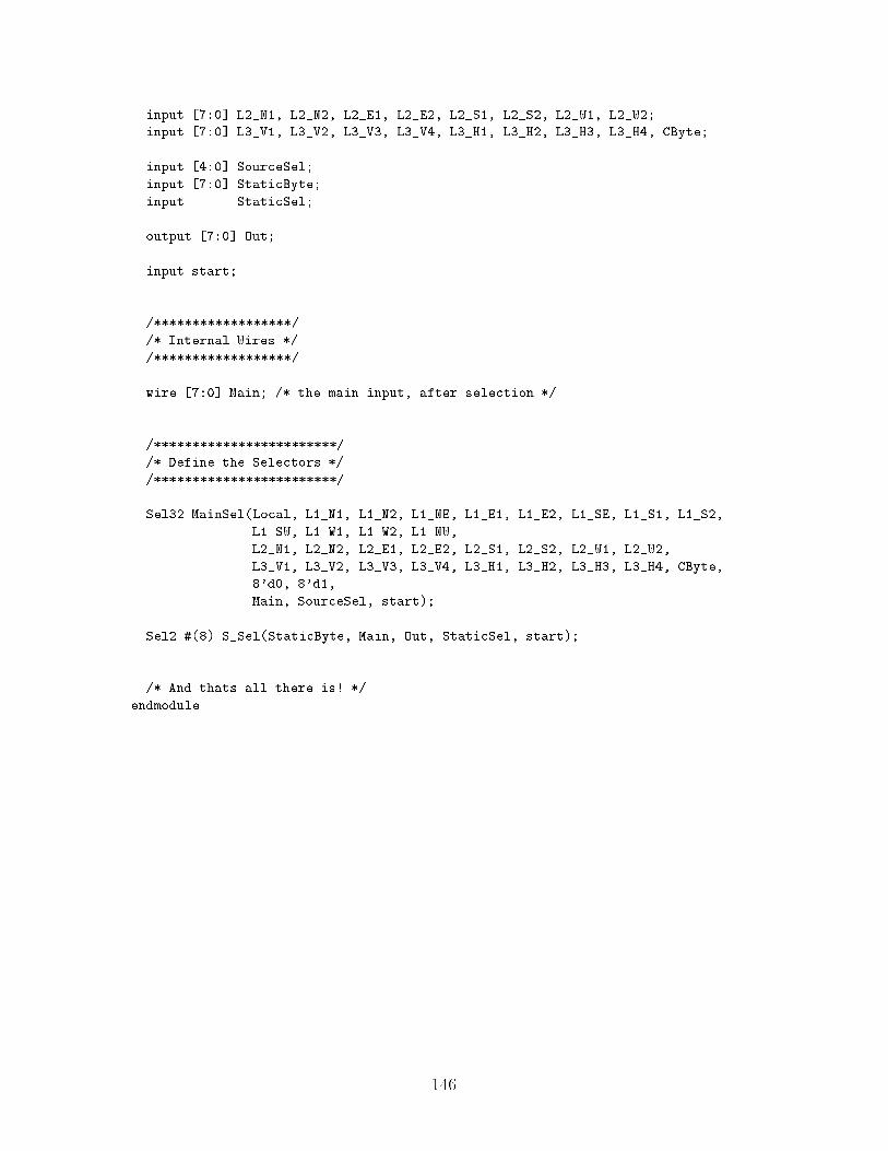
input [7:0] L2_N1, L2_N2, L2_E1, L2_E2, L2_S1, L2_S2, L2_W1, L2_W2;input [7:0] L3_V1, L3_V2, L3_V3, L3_V4, L3_H1, L3_H2, L3_H3, L3_H4, CByte;input [4:0] SourceSel;input [7:0] StaticByte;input StaticSel;output [7:0] Out;input start;/******************//* Internal Wires *//******************/wire [7:0] Main; /* the main input, after selection *//************************//* Define the Selectors *//************************/Sel32 MainSel(Local, L1_N1, L1_N2, L1_NE, L1_E1, L1_E2, L1_SE, L1_S1, L1_S2,L1_SW, L1_W1, L1_W2, L1_NW,L2_N1, L2_N2, L2_E1, L2_E2, L2_S1, L2_S2, L2_W1, L2_W2,L3_V1, L3_V2, L3_V3, L3_V4, L3_H1, L3_H2, L3_H3, L3_H4, CByte,8'd0, 8'd1,Main, SourceSel, start);Sel2 #(8) S_Sel(StaticByte, Main, Out, StaticSel, start);/* And thats all there is! */endmodule146

/* The following is necessary because this file may be read from many inlcudestatements and should be ignored on all but the first */`define selector_defined/*********************************//* Specifications for Selector.v *//*********************************//* A selector is is used to choose one input from a set of inputs and passthis value to the output (a multiplexor). There are three types ofselectors in this file. Sel2 is a 2 input selector, Sel8 is an 8 inputselector, Sel16 is a 16 input selector, and Sel32 is a 32 inputselector. Sel2 and Sel8 are parameterized in the size of the inputsand output, while Sel16 is fixed at 1-bit and Sel32 are fixed at8-bit I/O.Unfortunately, due to some problems (probably bugs) with VerilogXL it wasimpossible to construct a single device with parameterized inputs andbus-size, or even parameterized inputs. So, this is what was possible.Input start is a model-specific initialization input, used to force themodule to evaluate its inputs.*//***************//* Module Sel2 *//***************/module Sel2(In0, In1, Out, ctrl, start);/* Define the Bus Width parameter*/parameter BusW=1;/* The I/O sizes are set accordingly: */input [BusW-1:0] In0, In1;input ctrl;output [BusW-1:0] Out;reg [BusW-1:0] Out;input start;/******************//* Begin Selector *//******************/always @(ctrl or start)beginif (ctrl===0)assign Out = In0;elseassign Out = In1; 147

endendmodule/***************//* Module Sel8 *//***************/module Sel8(In0, In1, In2, In3, In4, In5, In6, In7,Out, ctrl, start);parameter BusW = 8;input [(BusW-1):0] In0, In1, In2, In3, In4, In5, In6, In7;input [2:0] ctrl;output [(BusW-1):0] Out;reg [(BusW-1):0] Out;input start;/******************//* Begin Selector *//******************/always @(ctrl or start)begincase(ctrl)5'd0: assign Out=In0;5'd1: assign Out=In1;5'd2: assign Out=In2;5'd3: assign Out=In3;5'd4: assign Out=In4;5'd5: assign Out=In5;5'd6: assign Out=In6;5'd7: assign Out=In7;default assign Out=8'd0;endcaseendendmodule/****************//* Module Sel16 *//****************/module Sel16(In, Out, ctrl, start);/* Note: For reasons I cannot understand (probably a bug), you needto put in a constant when concatinating inputs. Therefore thisinput is large to accomodate a constant in the high bit position */148

input [16:0] In;input [3:0] ctrl;output Out;reg Out;input start;/******************//* Begin Selector *//******************/always @(ctrl or start)beginassign Out = In[ctrl];endendmodule/****************//* Module Sel32 *//****************/module Sel32(In0, In1, In2, In3, In4, In5, In6, In7, In8, In9,In10, In11, In12, In13, In14, In15, In16, In17, In18, In19,In20, In21, In22, In23, In24, In25, In26, In27, In28, In29,In30, In31, Out, ctrl, start);input [7:0] In0, In1, In2, In3, In4, In5, In6, In7, In8, In9;input [7:0] In10, In11, In12, In13, In14, In15, In16, In17, In18, In19;input [7:0] In20, In21, In22, In23, In24, In25, In26, In27, In28, In29;input [7:0] In30, In31;input [4:0] ctrl;output [7:0] Out;reg [7:0] Out;input start;/******************//* Begin Selector *//******************/always @(ctrl or start)begincase(ctrl)5'd0: assign Out=In0;5'd1: assign Out=In1;5'd2: assign Out=In2;5'd3: assign Out=In3;5'd4: assign Out=In4;5'd5: assign Out=In5; 149

5'd6: assign Out=In6;5'd7: assign Out=In7;5'd8: assign Out=In8;5'd9: assign Out=In9;5'd10: assign Out=In10;5'd11: assign Out=In11;5'd12: assign Out=In12;5'd13: assign Out=In13;5'd14: assign Out=In14;5'd15: assign Out=In15;5'd16: assign Out=In16;5'd17: assign Out=In17;5'd18: assign Out=In18;5'd19: assign Out=In19;5'd20: assign Out=In20;5'd21: assign Out=In21;5'd22: assign Out=In22;5'd23: assign Out=In23;5'd24: assign Out=In24;5'd25: assign Out=In25;5'd26: assign Out=In26;5'd27: assign Out=In27;5'd28: assign Out=In28;5'd29: assign Out=In29;5'd30: assign Out=In30;5'd31: assign Out=In31;default assign Out=8'd0;endcaseendendmodule
150

/* The following is necessary because this file may be read from many inlcudestatements and should be ignored on all but the first */`define TSregister_defined/***********************************//* Specifications for TSregister.v *//***********************************//* A TSregister is a Time-Switch register. It is basically a normal clockedregister (always enabled), except that it can optionally enabled bycomparing an incoming cycle value to a stored configuration word. SeeTN130 for more details of this.TSregister is parameterized to the width of the Data.The TSregister structure also contains a reset signal which can force theregister to load zeros.The inputs to TSregister are:Data : The data inputCycle : The current cycleTSenable : Enables the Time-Switch LogicConfig : The configuration wordCLK : A clockstart : The simulation reset signalOut is the only output.*//*********************//* Module TSregister *//*********************/module TSregister (Data, Cycle, Out, TSenable, Config, CLK, start);/* Set default Data width */parameter Width = 8;/* Set I/O accordingly */input [Width-1:0] Data;input [3:0] Cycle, Config;input TSenable, CLK, start;output [Width-1:0] Out;reg [Width-1:0] Out;/******************/ 151

/* Internal State *//******************/reg Enable; /* The result of the Cycle-Config comparison *//*******************//* Maintain Enable *//*******************/initialbeginassign Enable = (Cycle == Config);end/****************//* Handle Start *//****************/always @(start)begin#1 Out = Data;end/*******************//* Everything Else *//*******************/always @(posedge(CLK))beginif (Enable || ~TSenable)begin#1 Out = Data;endendendmodule152

/***********************************//* Specifications for TSand.v *//***********************************//* A TSand is a Time-Switch AND gate. It takes a single input (parameterizedwidth) and bit-wise ANDs it with the result of a Time-Switch comparison.If TSenable is off, the comparison is always true.The inputs to TSregister are:Data : The data inputCycle : The current cycleTSenable : Enables the Time-Switch LogicConfig : The configuration wordstart : The simulation reset signalOut is the only output.*//****************//* Module TSand *//****************/module TSand (Data, Cycle, Out, TSenable, Config, start);/* Set default Data width */parameter Width = 1;/* Set I/O accordingly */input [Width-1:0] Data;input [3:0] Cycle, Config;input TSenable, start;output [Width-1:0] Out;reg [Width-1:0] Out;/****************//* Maintain Out *//****************/always @(start or TSenable or Cycle or Config)beginif (TSenable === 0)assign Out = Data;else if (Cycle === Config)assign Out = Data;elseassign Out = 0;end 153

endmodule
154

/* The following is necessary because this file may be read from many inlcudestatements and should be ignored on all but the first */`define tribuf_defined/*******************************//* Specifications for Tribuf.v *//*******************************//* Tribuf is a non-clocked tristate buffer, which passes on ctrl=1.Tribuf takes the bit-widths of the data lines as a parameter.Inputs:In : The InputCtrl : The control bitstart : A model-specific initialization input, used to force themodule to evaluate its inputs.Out : The Output*//*****************//* Module Tribuf *//*****************/module Tribuf(In, Ctrl, start, Out);/* Set the default parameter */parameter size = 1;input [size-1:0] In;input Ctrl, start;output [size-1:0] Out;reg [size-1:0] Out;integer i;/***************//* Begin model *//***************/always @(Ctrl or start)begincase (Ctrl)1'b0 :begin#1;deassign Out;for (i=0; i<size; i=i+1) 155

Out[i]=1'bz;end1'b1 : #1 assign Out = In;defaultbegin#1;deassign Out;for (i=0; i<size; i=i+1)Out[i]=1'bz;endendcaseendendmodule
156

/* The following is necessary because this file may be read from many inlcudestatements and should be ignored on all but the first */`define trireg_defined/*******************************//* Specifications for Trireg.v *//*******************************//* TriReg is a clocked tristate buffer (register), which passes on ctrl=1.TriReg takes the bit-widths of the data lines as a parameter.Inputs:In : The InputCtrl : The control bit.CLK : A clockstart : A model-specific initialization input, used to force themodule to evaluate its inputs.Out : The Output*//*****************//* Module Trireg *//*****************/module Trireg(In, Ctrl, CLK, start, Out);/* Set the default parameter */parameter size = 1;input [size-1:0] In;input Ctrl, CLK, start;output [size-1:0] Out;reg [size-1:0] Out;integer i;/***************//* Begin model *//***************/always @(posedge(CLK) or start)begincase (Ctrl)1'b0 :begin#1;for (i=0; i<size; i=i+1) 157

Out[i]=1'bz;end1'b1 : #1 Out = In;defaultbegin#1;for (i=0; i<size; i=i+1)Out[i]=1'bz;endendcaseendendmodule
158

Bibliography[1] Michael Bolotski, Thomas Simon, Carlin Vieri, Rajeevan Amirtharajah, andThomas F. Knight Jr. Abacus: A 1024 processor 8ns simd array. In AdvancedResearch in VLSI 1995, 1995.[2] Timothy Bridges. The gpa machine: A generally partitionable msimd architec-ture. In Proceedings of the Third Symposium on The Frontiers for MassivelyParallel Computations, pages 196{202. IEEE, 1990.[3] Dev C. Chen and Jan M. Rabaey. A recon�gurable multiprocessor ic for rapidprototyping of algorithmic-speci�c high-speed dsp data paths. IEEE Journal ofSolid-State Circuits, 27(12):1895{1904, December 1992.[4] Chi-Jui Chou, Satish Mohanakrishnan, and Joseph B. Evans. Fpga implemen-tation of digital �lters. In International Conference on Signal Processing Appli-cations and Technology, 1993.[5] Andr�e DeHon. Recon�gurable Architectures for General-Purpose Computing.PhD dissertation, Massachusetts Institute of Technology, Department of Elec-trical Engineering and Computer Science, 1996. Draft version - expected com-pletion: July, 1996.[6] Dave Epstein. Chromatic raises the multimedia bar. Microprocessor Report,9(14):23 �., October 23 1995.[7] Carla Golla, Fulvio Nava, Franco Cavallotti, Alessandro Cremonesi, and GiulioCasagrande. 30-msamples/s programmable �lter processor. IEEE Journal ofSolid-State Circuits, 25(6):1502{1509, December 1990.159

[8] Greg Goslin and Bruce Newgard. 16-TAP, 8-Bit FIR Filter Applications Guide.Xilinx, Inc., 2100 Logic Drive, San Jose, CA 95124, November 1994. http://www.xilinx.com/appnote/fir_filt.pdf.[9] Paul Gronowski, Peter Bannon, Michael Bertone, Randel Blake-Campos, Gre-gory Bouchard, WilliamBowhill, David Carlson, Ruben Castelino, Dale Donchin,Richard Fromm, Mary Gowan, Anil Jain, Bruce Loughlin, Shekhar Mehta,Jeanne Meyer, Robert Mueller, Andy Olesin, Tung Pham, Ronald Preston, andPaul Robinfeld. A 433mhz 64b quad-issue risc microprocessor. In 1996 IEEEInternational Solid-State Circuits Conference, Digst of Technical Papers, pages222{223. IEEE, February 1996.[10] Mark Horowitz, John Hennessy, Paul Chow, Glenn Gulak, John Acken, AnantAgarwal, Chorng-Yeung Chu, Scott McFarling, Steven Przybylski, StevenRichardson, Arturo Salz, Richard Simoni, Don Stark, Peter Steenkiste, StevenTjiang, and Malcom Wing. A 32b microprocessor with on-chip 2k byte instruc-tion cache. In 1987 IEEE International Solid-State Circuits Conference, Digstof Technical Papers, pages 30{31. IEEE, February 1987.[11] David Jones and David Lewis. A time-multiplexed fpga architecture for logic em-ulation. In Proceedings of the IEEE 1995 Custom Integrated Circuits Conference,pages 495{498. IEEE, May 1995.[12] Ethan Mirsky. Matrix micro-architecture. Transit Note 130, MIT Arti�cialIntelligence Laboratory, November 1995.[13] Ethan Mirsky and Andr�e DeHon. Matrix: A recon�gurable computing archi-tecture with con�gurable instruction distribution and deployable resources. InProceedings of the IEEE Workshop on FPGAs for Custom Computing Machines,April 1996.[14] Kouhei Nadehara, Miwako Hayashida, and Ichiro Kuroda. A Low-Power, 32-bitRISC Processor with Signal Processing Capability and its Multiply-Adder, volumeVIII of VLSI Signal Processing, pages 51{60. IEEE, 1995.160

[15] Gary J. Nutt. Microprocessor implementation of a parallel processor. In Proceed-ings of the Fourth Annual International Symposium on Computer Architecture,pages 147{152. ACM, 1977.[16] Peter Ruetz. The architectures and design of a 20-mhz real-time dsp chip set.IEEE Journal of Solid-State Circuits, 24(2):338{348, April 1989.[17] M. Shiraishi, M. Koizumi, A. Yamaguchi, and H. Hoike. User programmable16bit 50ns dsp. In Proceedings of the IEEE 1992 Custom Integrated CircuitsConference, pages 6.4.1{6.4.4. IEEE, May 1992.[18] Michael Slater. Microunity lifts veil on mediaprocessor. Microprocessor Report,9(14):11 �., October 23 1995.[19] Lawrence Snyder. An inquiry into the bene�ts of multigauge parallel computa-tion. In Proceedings of the 1985 International Conference on Parallel Processing,pages 488{492. IEEE, August 1985.[20] Edward Tau, Ian Eslick, Derrick Chen, Jeremy Brown, and Andr�e DeHon. A�rst generation dpga implementation. In Proceedings of the Third CanadianWorkshop on Field-Programmable Devices, pages 138{143, May 1995.[21] Jef van Meerbergen, Frank Welten, Frans van Wijk, Jan Stoter, Jos Huisken,Antoine Delaruelle, and Karel Van Eerdewijk. An 8 mips cmos digital signalprocessor. In 1985 IEEE International Solid-State Circuits Conference, Digst ofTechnical Papers, pages 84{85. IEEE, February 1986.[22] Alfred K. Yeung and Jan M. Rabaey. A 2.4 gops data-drivern recon�gurablemultiprocessor ic for dsp. In Proceedings of the 1995 IEEE International Solid-State Circuits Conference, pages 108{109. IEEE, February 1995.161