
CMUTs for medical imaging and therapy - Stanford University
12
Capacitive micromachined ultrasonic transducers for medical imaging and therapy This article has been downloaded from IOPscience. Please scroll down to see the full text article. 2011 J. Micromech. Microeng. 21 054004 (http://iopscience.iop.org/0960-1317/21/5/054004) Download details: IP Address: 69.181.114.70 The article was downloaded on 07/05/2011 at 23:42 Please note that terms and conditions apply. View the table of contents for this issue, or go to the journal homepage for more Home Search Collections Journals About Contact us My IOPscience
Transcript of CMUTs for medical imaging and therapy - Stanford University

Capacitive micromachined ultrasonic transducers for medical imaging and therapy
This article has been downloaded from IOPscience. Please scroll down to see the full text article.
2011 J. Micromech. Microeng. 21 054004
(http://iopscience.iop.org/0960-1317/21/5/054004)
Download details:
IP Address: 69.181.114.70
The article was downloaded on 07/05/2011 at 23:42
Please note that terms and conditions apply.
View the table of contents for this issue, or go to the journal homepage for more
Home Search Collections Journals About Contact us My IOPscience
IOP PUBLISHING JOURNAL OF MICROMECHANICS AND MICROENGINEERING
J. Micromech. Microeng. 21 (2011) 054004 (11pp) doi:10.1088/0960-1317/21/5/054004
Capacitive micromachined ultrasonictransducers for medical imaging andtherapyButrus T Khuri-Yakub and Omer Oralkan
EL Ginzton Laboratory, Center for Nanoscale Science and Engineering, Stanford University, Stanford,CA 94305-4088, USA
E-mail: [email protected]
Received 14 January 2011, in final form 18 March 2011Published 28 April 2011Online at stacks.iop.org/JMM/21/054004
AbstractCapacitive micromachined ultrasonic transducers (CMUTs) have been subject to extensiveresearch for the last two decades. Although they were initially developed for air-coupledapplications, today their main application space is medical imaging and therapy. This paperfirst presents a brief description of CMUTs, their basic structure and operating principles. Ourprogression of developing several generations of fabrication processes is discussed with anemphasis on the advantages and disadvantages of each process. Monolithic and hybridapproaches for integrating CMUTs with supporting integrated circuits are surveyed. Severalprototype transducer arrays with integrated front-end electronic circuits we developed andtheir use for 2D and 3D, anatomical and functional imaging, and ablative therapies aredescribed. The presented results prove the CMUT as a micro-electro-mechanical systemstechnology for many medical diagnostic and therapeutic applications.
(Some figures in this article are in colour only in the electronic version)
1. Introduction
Microfabricated devices and integrated circuits hold greatpromise for medical applications. Their high level ofintegration enables complete point-of-care devices at low cost.These devices also help achieve a compact form factor, higherresolution in imaging and therapy, and higher sensitivity.Micro-electro-mechanical systems (MEMS) technology ingeneral has found commercial success in inertial sensorsthat are adapted largely by the automotive, the mobilecommunications, and now by the gaming industries. Displaydevices, timing references, and microphones are some otherproduct groups MEMS technology has had an impact on.Pressure sensors originally developed for automotive andindustrial use represent one of the most widely used MEMSproducts in the medical field as part of implantable andcatheter-based blood pressure monitors. There is also a strongdemand for microfluidic devices for medical use. MEMS areincreasing their presence in consumer and medical business,adding to their strong base in automotive and industrialapplications.
Capacitive micromachined ultrasonic transducers(CMUTs) invented in the mid-1990s [Haller94] have comea long way in the last two decades and recently reached themarket for medical ultrasound imaging [Hitachi09]. Consid-ering the production of conventional ultrasonic transducerprobes alone, which amounts to a global market of about $1billion annually, one can speculate that CMUTs can be thenext big MEMS product in the medical field.
In the early years of research in this field, the main focuswas on basic device fabrication and understanding deviceoperation. Several fabrication processes based on standardsurface micromachining techniques have been developed[Jin98, Jin99, Schindel95, Haller96, Eccardt96, Eccardt97,Cianci02]. An alternative CMUT fabrication method basedon wafer bonding was developed later [Huang03]. Equivalentcircuit models for CMUTs have been developed to help withthe design of arrays for practical applications [Ladabaum98,Caronti02, Lohfink05]. Finite element analysis (FEA) hasbeen used to understand transducer characteristics (especiallycrosstalk issues), and to optimize transducer response[Bozkurt99, Wojcik00, Roh02, Yaralioglu05, Bayram07].
0960-1317/11/054004+11$33.00 1 © 2011 IOP Publishing Ltd Printed in the UK & the USA

J. Micromech. Microeng. 21 (2011) 054004 B T Khuri-Yakub and O Oralkan
1D and 2D array elements have been fully characterized[Oralkan99, Jin01]. Early imaging demonstrations wereperformed using systems built from discrete electroniccomponents [Oralkan02, Oralkan03]. In this paper, wefocus on the more recent developments in CMUT technologyincluding newly introduced fabrication processes, integratedfront-end circuits, and their applications in medical imagingand therapy.
The organization of the paper is as follows: the nextsection briefly describes the basic device structure andthe operating principle. In section 3, the progression ofCMUT fabrication processes is summarized. Section 4details advantages and disadvantages of several approaches tointegrate transducer arrays and supporting electronics circuits.Examples of implemented devices for various imaging andtherapeutic applications are presented in sections 5 and 6,respectively.
2. CMUT: basic structure and operating principle
The basic building block of a CMUT is a capacitor cell thatconsists of a thin movable plate suspended over a vacuumgap. A metal layer on top of the thin plate or the thinplate itself, if conductive, forms the top electrode of thecapacitor. The underlying conductive substrate acts as thebottom electrode. When a dc voltage is applied betweenthese two electrodes the top plate is attracted toward thesubstrate by the electrostatic force. A mechanical restoringforce due to the stiffness of the plate resists the attraction.Driving the capacitor with an alternating voltage generatesultrasound. If the movable top plate is subjected toultrasound pressure, an electrical current is generated dueto the capacitance change under constant bias voltage. Theamplitude of this current is a function of the frequency ofthe incident wave, the bias voltage and the capacitance of thedevice. The key point to be able to realize a competitiveelectrostatic transducer is to maintain an electric field in thegap with the strength on the order of 108 V cm−1 or higher.This is also the very reason why MEMS technology was theenabler for this century-old idea of electrostatic transductionfor ultrasound generation and detection. As will be explainedin the next section, this high electric field, which makes thisdevice so competitive, also necessitates extreme care in designto avoid any reliability issues related to dielectric charging andbreakdown.
The dimensions, the shape and the mechanical propertiesof the thin plate mainly determine the operating frequencyfor the described conventional CMUT structure. Therefore,many capacitor cells are connected in parallel to implementtransducers and arrays of transducers in the desired size andshape operating at the desired frequency. For medical use thesilicon-based transducer is usually covered by a thin layerof elastic polymer to provide electrical insulation withoutsignificantly affecting the performance of the device [Lin10].One of the major advantages of CMUTs compared to theirpiezoelectric counterparts is the wide bandwidth. Whenoperated in immersion, the transducer’s mechanical plateimpedance is much smaller than the loading impedance over
a large frequency range, resulting in very broad bandwidth.The lower cutoff frequency is determined by the springconstant. As the spring constant increases, the bandwidthof the transducer decreases. The higher cutoff frequency isdetermined by the membrane mass and the mass loading ofthe immersion medium as well as the higher order resonantmodes of the plate. Other well-known advantages of MEMStechnology such as low cost, amenability to integration withelectronic circuits, and miniaturization are all valid for CMUTsas well.
3. CMUT fabrication
Several process flows have been developed by various researchgroups to implement CMUT arrays using standard surface andbulk micromachining techniques. This section summarizessome of the CMUT fabrication process flows we developedto progressively address several performance and reliabilityimprovements. The details of these processes are not explainedhere, but rather the key points are mentioned and the readeris referred to the related literature. Also graphically only thefinal device structure is depicted for each described process infigure 1 instead of showing the entire process flow.
3.1. Sacrificial release process
For nearly a decade, from 1993 to 2003, we used process flowsbased on standard surface micromachining, particularly onsacrificial release. A variety of the sacrificial release processeshave been published based on the same basic principle offorming a cavity underneath a thin plate by first depositingor growing a sacrificial layer on the carrier substrate and thenselectively removing the sacrificial layer using an appropriateetchant, specifically chosen to etch the sacrificial layer materialbut not to etch the plate layer (figure 1(a)) [Ergun05]. Differentsacrificial layer, plate and substrate material combinationshave been used to fabricate CMUTs. An extended version ofthis process includes through-wafer via interconnections fromthe front side of the substrate to the backside. Deep reactive ionetching (DRIE) enables a dense array of high-aspect ratio viasin silicon that are filled with conductive material such as dopedpolysilicon to provide electrical connectivity from the front tothe back of the substrate [Cheng02]. The major shortcomingof the sacrificial release process is the poor control overthe uniformity, absolute thickness and mechanical propertiesof deposited layers affecting important device parameterssuch as the gap height, the plate thickness and the residualstress [Lin07].
3.2. Wafer bonding process
To improve on the process control and repeatability issueslimiting the sacrificial release process and to reduce the processcomplexity, we developed a wafer bonding-based process tofabricate CMUTs. A number of variations on the bondingprocess are listed below with continuing enhancement inperformance.
2

J. Micromech. Microeng. 21 (2011) 054004 B T Khuri-Yakub and O Oralkan
(a) (b) (c)
(d ) (e) (f )
Figure 1. Schematic cross-sections for different CMUT structures. (a) CMUT fabricated using the sacrificial release process. (b) CMUTfabricated using the simple wafer bonding process. (c) CMUT fabricated using the LOCOS process. (d) CMUT fabricated using thethick-buried-oxide process. (e) CMUT with added mass on its plate. (f ) CMUT with the compliant post structure.
3.2.1. Simple wafer bonding. This process begins withtwo wafers: a prime quality silicon wafer and a silicon-on-insulator (SOI) wafer. The cavity is defined on the primewafer by selectively etching thermally grown oxide down tothe substrate followed by a second thermal oxidation to growthe insulation layer. Following an RCA clean and surfaceactivation, the SOI wafer and the prime wafer are broughttogether in vacuum. The wafers are then immediately annealedat high temperature (∼1100 ◦C) to form strong covalentbonds. The handle portion and the buried oxide layer of theSOI wafer are later removed, leaving a thin single crystalsilicon plate suspended over the cavities. Finally electricalconnections to the substrate are provided through openingsin the oxide layer and individual elements are defined byetching isolation trenches in the silicon plate (figure 1(b))[Huang03]. To provide electrical connection to each elementin a 2D array from the backside of the substrate, we alsodeveloped an interconnect technology compatible with thewafer bonding process. In this approach, deep trenchesetched in the silicon substrate define silicon pillars that serveas the individual interconnects to each element [Zhuang06].The most important improvement enabled by wafer-bondingprocess is that the thickness, uniformity and mechanicalproperties of the plate are well controlled, thanks to the singlecrystal silicon device layer of the SOI wafer. This processalso provides improved control over the gap height since it ismainly defined by thermal oxidation. However, the minimumgap height is limited by the thickness of the initial oxidelayer. As a result, this structure is compromised by reducedbreakdown voltage and increased parasitic capacitance in thearea between the cells of the CMUT. Another drawbackin the described approach is related to the trench-isolatedinterconnect structure, which is prone to electrical shortcircuits due to possible contamination both on the front andbacksides of the devices that might occur in subsequentpackaging steps.
3.2.2. LOCOS process. An extended insulation layerstructure in the post area would address the low breakdown
voltage and high parasitic capacitance issues associated withthe first-generation wafer-bonded CMUTs described in theprevious subsection [Kupnik07]. We used the local oxidationof silicon (LOCOS), a widely used process step in standardIC processing, to form the extended post region (figure 1(c))[Park08]. This process also features an excellent gap heightcontrol achieved by patterning the silicon substrate inside thecavity via thermal oxidation, and then forming the oxide postsby a selective thermal oxidation step using the conventionalLOCOS process. We demonstrated devices fabricated usingthis approach for chem/bio sensor applications [Lee10], buthave not used this process for 2D imaging arrays that wouldrequire a compatible through-wafer interconnect technology.
3.2.3. Thick-buried-oxide process. More recently wedeveloped a structure and the associated process flow thatconfines and isolates the CMUT bottom electrode only to theregion under the gap where the high electric field is desired[Kupnik10], so that the probability of dielectric breakdown andparasitic capacitance in the post region can be minimized. Thisstructure also includes through-wafer via interconnects foraccessing each element from the backside. The key componentin this approach is an SOI wafer with a thick buried oxidelayer. Vertical insulation trenches are used on the device layerof this SOI wafer to form completely insulated silicon bottomelectrodes below the active plate region in each CMUT cell.The hot electrode is provided through an opening in the thickburied oxide layer filled using doped polycrystalline siliconor any other electrically conductive material (figure 1(d)).This arrangement provides each cell with its own individualconnection to the hot electrode.
3.2.4. Piston–CMUT structure and process. We havedeveloped other variations of the described basic devicestructures and process flows for various performanceimprovements. One such improvement is related toengineering the plate profile to approximate the membranemotion to an ideal piston-like motion. We have shown
3

J. Micromech. Microeng. 21 (2011) 054004 B T Khuri-Yakub and O Oralkan
an improved transmit and receive performance, and widerfractional bandwidth using a plate structure with an addedcenter mass compared to a classical CMUT structure withuniform membrane thickness (figure 1(e)) [Huang09]. Sucha structure can be implemented by forming the central massby etching the device layer of an SOI layer or by platingmetal on top of the plate structure. Another recent improveddevice structure we developed is based on a rigid plateconnected to a substrate using relatively long and narrow posts,providing the spring constant for the movement of the plate(figure 1(f )) [Nikoozadeh10A]. The resulting plate motionresembles that of an ideal piston. This structure not onlyimproves the average displacement but also results in asignificantly improved fill factor because the non-active plateanchor areas that are inevitable in a conventional CMUTstructure are eliminated in this case. Both the added centralmass and the compliant post approaches also separate the massand spring components of the transducer and enable a moreflexible design space.
4. Integration with electronic circuits
Close integration of ultrasonic transducer arrays andsupporting integrated circuits is highly desired in manyapplications, especially for transducer arrays with smallelements such as in 2D arrays and arrays for use at the end of acatheter. In current conventional ultrasonic imaging systems,the array is located in a hand-held probe, which is connected tothe main processing unit via a cable bundle. Transmit pulsersand receive amplifiers are located in the main processingunit. Because of the small size and small capacitance oftransducer elements in a 2D array (piezoelectric or capacitive),the receiver electronics must be close to the transducer array, sothat the additional capacitance introduced by the cable wouldnot degrade the signal quality. Furthermore, multiplexing andbeamforming circuitry can also be integrated with the arrayto minimize the number of active electronic channels and thenumber of physical connections between the probe and thebackend system.
For integrating CMUT arrays with electronic circuitsseveral methods developed for a variety of MEMS applicationshave been adapted. These methods can be categorized in twomain groups: monolithic and multichip (hybrid) approaches.Monolithic integration is realized by building CMUTs andelectronics concurrently, or by building CMUTs on finishedelectronic wafers. For multichip (hybrid) integration, anintegrated circuit die and a CMUT die can be directly bondedon top of each other or a flexible or rigid intermediate substratemay be used.
4.1. Monolithic integration
4.1.1. Co-processing. One method to monolithicallyintegrate CMUTs and electronic circuits is to fabricate bothcomponents concurrently using a standard or minimallymodified process. A BiCMOS process using 16 maskshas been used with only minor modifications including anadditional photolithography step and sacrificial layer etching
to fabricate CMUTs side-by-side with electronic circuitson the same substrate [Eccardt97]. Although this methodoffers a cost-effective means of integration, it has two majorlimitations: (1) the transducer element area is shared byelectronic circuits or interconnects. (2) The device dimensionsin the vertical direction are limited by the film thicknessesavailable in the process used to make electronic circuits.
4.1.2. Post-processing by low-temperature surfacemicromachining. A second monolithic integration techniqueis to fabricate the electronic circuits first using a standardfoundry process and then build CMUTs on top of finishedelectronics by further processing. This post-processing iskept minimal in a process called ‘CMUT-in-CMOS’ byaugmenting a standard foundry process only with two blanketpost-process steps for sacrificial etching and cavity sealing[Cheng09]. Although this process is fairly simple, itstill suffers from the limitations on the device dimensionsin the vertical direction because layers available in thestandard foundry process are utilized as sacrificial layer.More complicated processing including surface passivation,planarization, opening of contacts to electronics, and furthersuccessive thin film deposition and etching steps is alsodemonstrated to define the CMUT plates with greater precisionand control [Noble02, Daft04, Gurun08]. This approach hasgood area utilization and more control over device dimensions.However, processing techniques for making CMUTs are stilllimited, mainly due to temperature constraints set by theexisting metal lines on the electronics.
4.1.3. Post-processing by low-temperature direct waferbonding. We have recently demonstrated CMUTs fabricatedby low temperature wafer bonding indicating that CMUTscan be directly built on a finished CMOS substrate by waferbonding [Tsuji10]. This approach brings the advantages ofthe wafer bonding process such as control over the platethickness, and process simplicity and provides a monolithicintegration solution without going through the complexity ofpost-CMOS sacrificial release process explained in section4.1.2. In this low-temperature bonding process we used a thintitanium layer for electrical via-contact to CMOS substrate aswell as an adhesion layer for wafer bonding. The gap heightis set by the total thickness of the titanium adhesion layer andthe passivation layer on the CMOS wafer.
4.2. Multichip integration
4.2.1. Chip-to-chip bonding. One can optimize fabricationprocesses for both CMUTs and front-end integrated circuitsby making both components on separate substrates. In thiscase, CMUTs need through-wafer via interconnections fromthe front side of the substrate to the backside as explainedin section 3. CMUT arrays can then be bonded directly onelectronics using well-established flip–chip bonding processes[Wygant08]. Direct bonding usually requires that theelectronics die area to be greater than the CMUT die area, sothat peripheral pads on the electronics die will be accessibleto provide connections between the front-end circuits and thebackend system.
4

J. Micromech. Microeng. 21 (2011) 054004 B T Khuri-Yakub and O Oralkan
4.2.2. Bonding on intermediate substrates. Using anintermediate substrate makes the size of the CMUT andelectronics dice independent and could be desirable in thefollowing cases: (1) In standard IC processing a reticle isstepped across a whole wafer to transfer the reticle imagepattern to adjacent areas on the wafer. The reticle size limits themaximum size of a chip. Therefore, to implement very largeCMUT arrays, electronics or both electronics and the CMUTarray should be implemented by tiling several unit blocks. Thisapproach also helps improve the overall yield one can achieve.A large array was recently demonstrated with several 16 ×16 2D CMUT arrays flip–chip bonded on one side of a rigidinterposer and several application specific integrated circuits(ASIC) bonded on the other side [Wodnicki09]. In a similarfashion we also demonstrated a rigid interposer with a single32 × 32 2D CMUT array on one side and four custom 16 × 16ASICs on the other side (figure 2(a)). In both demonstrationsthe interposer provides the electrical connections between theCMUT array and the electronics and also to the externalbackend system. (2) Using a flexible intermediate substrate,the overall form factor of an integrated ultrasound probe canbe minimized. We used this approach by folding an eight-legged flex circuit where each leg had a flip–chip-bonded 8-channel front-end IC to address a 64-element CMUT ringarray for forward-looking catheter-based intracardiac imaging(figure 2(b)). Using this approach we were able to interface aCMUT array with 3 mm2 silicon area with electronic circuitsoccupying a total area of 8 mm2 silicon without increasing thefinal catheter size [Nikoozadeh10B].
5. Imaging applications
Ultrasound is a non-ionizing radiation, and hence is wellaccepted for diagnostic use even in obstetrical applications.The image presentation is in real time, allowing the studyof moving internal structures. Ultrasonic imaging equipmentis cost-effective and portable. All these features have madeultrasound a widely used imaging modality in medicine.Ultrasound is particularly useful in imaging cardiac structures,the vascular system, the fetus and uterus, abdominal organssuch as the liver, kidneys and gall bladder, and the eye.In this section, we present imaging results obtained usingCMUT arrays in different shapes and forms to demonstratethe potential of CMUT technology for several diagnostic andtherapy guiding applications.
5.1. Conventional 2D cross-sectional imaging
Today, the most common form of ultrasonic transducers usedfor medical imaging is the 1D array, which allows electronicfocusing and steering of ultrasonic beams within an azimuthalplane resulting in 2D cross-sectional images. We havebuilt 1D CMUT arrays of equivalent size, channel countand operating frequency to state-of-the-art medical arraysemploying piezoelectric transducers. Early versions of thesearrays were fabricated using the sacrificial release process andcontained 128 individually addressable elements, each 6 mmhigh by 200 μm wide, with an element pitch of 250 μm.
(a)
(b)
Figure 2. Multichip hybrid integration. (a) Left panel top:a 32 × 32 2D CMUT array flip–chip bonded on the top-side of arigid interposer. Left panel bottom: four ICs flip–chip bonded onthe bottom side of the interposer. Right panel: the cross-sectionalview of the multichip assembly. (b) Eight ICs and a 64-elementCMUT ring array flip–chip bonded on flexible printed circuit board.Each leg of the flexible PCB is folded for placement in the cathetertip [Nikoozadeh10B].
The experimental imaging results were in excellent agreementwith the simulations, thus confirming the near ideal response ofthese transducer arrays [Oralkan02]. More recently, we havefabricated 128-element 1D arrays using the wafer bondingprocess. These arrays have a 300 μm element pitch, are3.3 mm long in the elevation direction and operate at acenter frequency of 7.5 MHz with 100% fractional bandwidth(figure 3). 1D CMUT arrays that we fabricated using thewafer-bonding technology were also used with commercialscanners to obtain clinical images [Mills03]. Comparedto equivalent piezoelectric transducer arrays, CMUT arraysdemonstrated an improved resolution and as a result betterdefinition of fine structures in the carotid artery and the thyroidgland. More recently, Hitachi Corporation announced the firstsuccessful commercialization of a CMUT-based 1.5D arrayfor conventional 2D cross-sectional imaging, manifesting thelevel of maturity CMUT technology has reached [Hitachi09].
5.2. 3D Imaging using 2D arrays
A 2D transducer array allows electronic focusing and steeringof ultrasonic beams both in azimuthal and elevationaldirections to enable real-time 3D imaging. Progress inthis field has been slow due to several challenges such as
5

J. Micromech. Microeng. 21 (2011) 054004 B T Khuri-Yakub and O Oralkan
Figure 3. A 132-element 1D CMUT array fabricated using thesimple wafer bonding process.
manufacturing large 2D arrays with thousands of elements,providing front-end integrated circuits to preserve the signalintegrity from very small transducer elements, dealing witha large number of electronic channels, and processing a largeamount of data in real time. Recently, several major ultrasoundsystem manufacturers have introduced 2D array-based 3Dimaging platforms to the market. These systems employelectronic multiplexing and beamforming circuitry next to thetransducer array to reduce the number of active electronicchannels [Savord03] so that standard backend systems withlimited number of channels, i.e. 128–256 channels, can be usedfor image formation. The currently commercially available2D arrays consist of 2000–3000 elements fabricated fromexpensive materials such as single crystal piezoelectrics.
CMUT technology is especially promising for realizationof large 2D arrays that can be lithographically defined. Asearly as 1999, we demonstrated a 128 × 128-element 2Darray where each element was electrically accessible fromthe backside with a through-wafer via interconnects. Ourfirst 3D imaging results were obtained using a 8 × 16element portion of this array flip–chip bonded to a fan-outdie used along with the PC-based data acquisition systemdesigned for 1D CMUT arrays [Oralkan03]. Following thiswork, we developed a volumetric ultrasound imaging systembased on a 16 × 16-element, 250 μm pitch 2D CMUTarray for 3D endoscopic imaging. The array was flip–chip bonded to a custom IC that comprises the front-endelectronics (figure 4(a)). An output pressure of 330 kPa fora 25 V unipolar pulse and a minimum detectable pressure of1 mPa Hz−1/2 were measured for the integrated prototypeoperating at a center frequency of 3 MHz. Using thissystem, we obtained volumetric images of a wire phantom(figure 4(b)) and a vessel phantom. Although everyelement has its own dedicated pulser and amplifier, onlya single element was selected at a time to simplify theinitial implementation of this first-generation front-end IC,as discussed earlier. Thus, classic synthetic aperture imagereconstruction was used [Wygant08]. We also demonstratedreal-time images with a second-generation front-end IC wedesigned with transmit beamforming capability (figure 5(a))[Wygant09]. A nylon wire phantom (figure 5(b)) and a left
(a)
(b)
Figure 4. (a) A 16 × 16 2D CMUT array flip–chip bonded on thefirst-generation custom front-end IC. (b) 3D rendered image of awire phantom obtained in synthetic aperture mode with a 5 MHzarray (the phantom is schematically shown in the inset).
atrial model of the heart made of latex were imaged usingthe described 2D CMUT array integrated with this second-generation IC. Currently, we are integrating four front-endICs with a 32 × 32-element 2D array using an interposer asexplained in section 4 to improve the image resolution.
5.3. Catheter-based imaging
Forward-viewing ultrasound volume images are desired formany intravascular and intracardiac applications such asguiding treatment of chronic total occlusion, helping stentdeployment, and monitoring ablation procedures in the heart.An annular ring is the preferred geometry for transducerarrays because it can provide a 3D volume image withoutthe complexity of a fully populated 2D array. However, it isvery challenging to implement this geometry in a very smallscale (1–2 mm) using the existing piezoelectric transducertechnology [Wang02]. On the other hand, CMUT arrayscan be made in any arbitrary geometry with very small
6
J. Micromech. Microeng. 21 (2011) 054004 B T Khuri-Yakub and O Oralkan
(a)
(b)
Figure 5. (a) A 16 × 16 2D CMUT array flip–chip bonded on thesecond-generation custom front-end IC with transmit beamformingcapability. (b) 3D rendered image of a wire phantom with a2.5 MHz array.
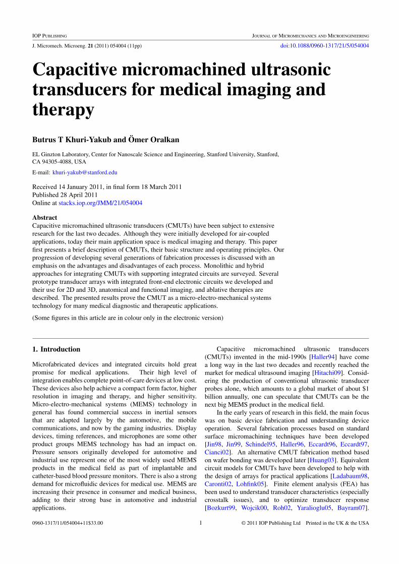
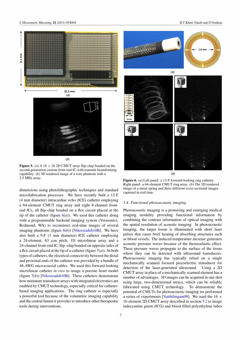
dimensions using photolithographic techniques and standardmicrofabrication processes. We have recently built a 12-F(4 mm diameter) intracardiac echo (ICE) catheter employinga 64-element CMUT ring array and eight 8-channel front-end ICs, all flip–chip bonded on a flex circuit placed at thetip of the catheter (figure 6(a)). We used this catheter alongwith a programmable backend imaging system (Verasonics,Redmond, WA) to reconstruct real-time images of severalimaging phantoms (figure 6(b)) [Nikoozadeh10B]. We havealso built a 9-F (3 mm diameter) ICE catheter employinga 24-element, 63 μm pitch, 1D microlinear array and a24-channel front-end IC, flip–chip bonded on opposite sides ofa flex circuit placed at the tip of a catheter (figure 7(a)). In bothtypes of catheters, the electrical connectivity between the distaland proximal ends of the catheter was provided by a bundle of48-AWG microcoaxial cables. We used this forward-lookingmicrolinear catheter in vivo to image a porcine heart model(figure 7(b)) [Nikoozadeh10B]. These catheters demonstratehow miniature transducer arrays with integrated electronics areenabled by CMUT technology, especially critical for catheter-based imaging applications. The ring catheter is especiallya powerful tool because of the volumetric imaging capabilityand the central lumen it provides to introduce other therapeutictools during interventions.
(a)
(b)
Figure 6. (a) Left panel: a 12-F forward-looking ring catheter.Right panel: a 64-element CMUT ring array. (b) The 3D renderedimage of a metal spring and three different cross-sectional imagescaptured in real time.
5.4. Functional photoacoustic imaging
Photoacoustic imaging is a promising and emerging medicalimaging modality providing functional information bycombining the contrast information of optical imaging withthe spatial resolution of acoustic imaging. In photoacousticimaging, the target tissue is illuminated with short laserpulses that cause brief heating of absorbing structures suchas blood vessels. The induced temperature increase generatesacoustic pressure waves because of the thermoelastic effect.These pressure waves propagate to the surface of the tissuewhere they can be detected with ultrasound transducers.Photoacoustic imaging has typically relied on a singlemechanically scanned focused piezoelectric transducer fordetection of the laser-generated ultrasound. Using a 2DCMUT array in place of a mechanically scanned element has anumber of advantages. 3D images can be acquired in one shotusing large, two-dimensional arrays, which can be reliablyfabricated using CMUT technology. To demonstrate thepotential of CMUTs for photoacoustic imaging we performeda series of experiments [Vaithilingam09]. We used the 16 ×16-element 2D CMUT array described in section 5.2 to imageindocyanine green (ICG) and blood filled polyethylene tubes
7

J. Micromech. Microeng. 21 (2011) 054004 B T Khuri-Yakub and O Oralkan
(a)
(b)
Figure 7. (a) Left panel: the 9-F forward-looking microlinearcatheter. Right panel: a 24-element CMUT microlinear array. (b) A2D image obtained with the CMUT microlinear array in vivo in apig heart.
embedded in chicken breast tissue (figure 8(a)). We useddouble-sided laser illumination at a wavelength of 775 nm togather the photoacoustic data since the peak ICG absorptionis at this wavelength for the concentrations used. The16 × 16 CMUT array and tank were mounted on a precision x–y translational stage to enable planar scanning and emulationof a 64 × 64-element CMUT array. An image reconstructedfrom this data is equivalent to that of an image reconstructedusing a 64 × 64-element CMUT array. The pulse-echoand photoacoustic images are shown in figures 8(b) and (c),respectively. The ability to obtain simultaneous pulse-echoand photoacoustic images enable to get both anatomical andfunctional images at once. Recently, we demonstrated thatthe photoacoustic imaging depth could be extended up to5 cm without exceeding the permitted laser exposure limit(20 mJ cm−2 per pulse) mainly enabled by the superiornoise performance of 2D arrays with integrated front-endcircuits [Ma10].
6. Therapeutic applications
Ultrasound is widely used as a diagnostic imaging modality inmany clinical applications and has recently received increasedattention and acceptance as a therapeutic tool. A significantadvantage of using high intensity focused ultrasound (HIFU)over other modalities, e.g. radio-frequency (RF) ablation, isthe ability to generate a precise ablation pattern deep intissue, with no effect on the surrounding structures. Today
(a)
(b)
(c)
Figure 8. Photoacoustic images of the chicken breast phantom,reconstructed using the data from a 64 × 64 aperture. (a) Schematicof tubes embedded in the chicken breast phantom. (b) 3D renderedpulse-echo image (grayscale). (c) 3D rendered photoacoustic image(red).
most HIFU systems in use employ spherical shell focusedtransducers operating in the range of 1–4 MHz and arebased on piezoelectric materials such as PZT-8 and PZT-4[Ebbini99]. More recently, phased array applicators weredeveloped for HIFU. Phased arrays offer improved controlfeatures that are needed for precise lesion formation at a depthin the presence of tissue inhomogeneity and patient/applicatormovement. Use of large arrays also enables the deliveryof high acoustic power to the target area without generatinghigh intensities on the surface of the transducer. As a result,the ultrasound energy passes harmlessly through overlyingtissues en route to a tightly focused target area. HIFUapplications can greatly benefit from the CMUT technologybecause of the ability to make large transducer arrays usingbasic microlithographic techniques. CMUTs also do not sufferfrom self-heating effects because they have much less internal
8

J. Micromech. Microeng. 21 (2011) 054004 B T Khuri-Yakub and O Oralkan
loss compared to their piezoelectric counterparts and generatedheat can be easily dissipated since they are fabricated fromhighly thermally conductive silicon. This makes CMUTs wellsuited for high power and continuous wave (CW) applicationslike HIFU. Our preliminary experimental results showed thatCMUTs can be used in CW operation for extended periods oftime, e.g. >90 min, while producing acoustic pressures around2 MPa peak-to-peak on the surface [Wong08, Wong10]. Oneof the most important design criteria for HIFU CMUTs isthe current handling capability. Using thick doped siliconmembranes and additional metal traces, the ohmic losses areminimized to avoid device failure by electromigration or self-heating. In contrast to a common misconception, plate fatigueis not a major failure mechanism in HIFU CMUTs. First,the deflection needed to obtain 1 MPa at 10 MHz is only10 nm. Second, even with other types of MEMS devicessuch as the digital micromirror devices with ±10◦ hingemovement, >1012 cycles of operation have been demonstrated[Douglass98]. The reason for fatigue not being a major sourceof failure in small structures is that the accumulation of densityof dislocations is not large enough to form fatigue-relatedcracks. The macroscopic model for fatigue, which is based ondislocations piling up at the surface of a material and this waycreating stress concentrations at sharp corners and scratches,does not hold for small structures.
We fabricated CMUT arrays specifically designed forHIFU applications using a high temperature direct fusionbonding process. Using one of the unfocused 2.5 MHz CMUTtransducers with a size of 2.5 mm by 2.3 mm, we demonstratedheating in a gel phantom with unfocused ultrasound by14–18 ◦C over a 2.5–5 min time. The heating produced a‘cumulative equivalent minutes at 43 ◦C (CEM43)’ of over128 min in a sizeable volume. This is the threshold necrosisvalue for cardiac tissue. This experiment indeed shows that thisdevice delivers output pressures needed for HIFU applications,and that it could potentially necrose a sizeable volume ofcardiac tissue to a depth of approximately 1 cm. The acousticalto electrical efficiency of the CMUT used in this study wasmeasured as 68% [Wong08].
7. Conclusion
The history of CMUTs is now approaching two decades.From being an interesting and efficient air transducer, theCMUT is now considered as a major platform technologyto realize many medical diagnostic and therapeutic devices.In the last decade by concentrating on the close integration ofCMUTs with supporting electronic circuits we demonstratedmany miniature imaging devices and supporting systemsfor endoscopic and intracardiac imaging. Although thepotential of CMUTs for diagnostic imaging is well understood,the potential for therapeutic applications in some measureis not fully explored. As a result one of the importantfuture research directions in this field will be using CMUTsfor integrated multimodal imaging and therapy. Anotheremerging application field that has not been covered in thispaper is sensing, in particular using CMUTs for medicalsensor applications based on the principles of mass loading and
acoustic wave propagation. In parallel with this expansion ofthe application field, there will also be many improvementson the device structures and fabrication processes to turnthis exciting research field into a complete commercialsuccess. Some of the ongoing efforts in this direction includedeveloping new device structures to achieve higher acousticpressures in transmit using low to moderate level of electricalexcitations, improving the electrical reliability and increasingthe level of integration with electronic circuits. However,as the recent introduction of CMUT-based imaging probesinto the market suggests, the complete commercial success ofCMUT technology depends more on finding applications withhigh volume markets, rather than overcoming technologicalhurdles.
Acknowledgments
This work was supported by the National Institute of Healthunder grants CA99059, CA134720, CA121163 and HL67647.
References
[Haller94] Haller M I and Khuri-Yakub B T 1994 A surfacemicromachined electrostatic ultrasonic airtransducer Proc. IEEE Ultrason. Symp.pp 1241–4
[Hitachi09] www.hitachi-medical.co.jp/medix/pdf/vol51/P31-34.pdf
[Jin98] Jin X, Ladabaum I and Khuri-Yakub B T 1998The microfabrication of capacitive ultrasonictransducers IEEE/ASME J. Microelectromech.Syst. 7 295–302
[Jin99] Jin X, Ladabaum I, Degertekin F L, Calmes Sand Khuri-Yakub B T 1999 Fabrication andcharacterization of surface micromachinedcapacitive ultrasonic immersion transducersIEEE/ASME J. Microelectromech. Syst.8 100–14
[Schindel95] Schindel D W and Hutchins D A 1995 The designand characterization of micromachinedair-coupled capacitance transducers IEEETrans. Ultrason. Ferroelectr. Freq. Control42 42–50
[Haller96] Haller M I and Khuri-Yakub B T 1996 A surfacemicromachined electrostatic ultrasonic airtransducer IEEE Trans. Ultrason. Ferroelectr.Freq. Control 43 1–6
[Eccardt96] Eccardt P C, Niederer K, Scheiter T and HierholdC 1996 Surface micromachined ultrasoundtransducers in CMOS technology Proc. IEEEUltrason. Symp. pp 959–62
[Eccardt97] Eccardt P C, Niederer K and Fischer B 1997Micromachined transducers for ultrasoundapplications Proc. IEEE Ultrason. Symp.pp 1609–18
[Cianci02] Cianci E, Foglietti V, Caliano G and PappalardoM 2002 Micromachined capacitive ultrasonictransducers fabricated using silicon oninsulator wafers Microelectron. Eng.61–62 1025–9
[Huang03] Huang Y, Ergun A S, Haeggstrom E, Badi M Hand Khuri-Yakub B T 2003 Fabricatingcapacitive micromachined ultrasonictransducers with wafer-bonding IEEE/ASMEJ. Microelectromech. Syst. 12 128–37
9

J. Micromech. Microeng. 21 (2011) 054004 B T Khuri-Yakub and O Oralkan
[Ladabaum98] Ladabaum I, Jin X, Soh H T, Atalar Aand Khuri-Yakub B T 1998 Surfacemicromachined capacitive ultrasonictransducers IEEE Trans. Ultrason. Ferroelectr.Freq. Control 45 678–90
[Caronti02] Caronti A, Caliano G, Iula A and Pappalardo M2002 An accurate model for capacitivemicromachined ultrasonic transducers IEEETrans. Ultrason. Ferroelectr. Freq. Control49 159–68
[Lohfink05] Lohfink A and Eccardt P-C 2005 Linear andnonlinear equivalent circuit modeling ofCMUTs IEEE Trans. Ultrason. Ferroelectr.Freq. Control 52 2163–72
[Bozkurt99] Bozkurt A, Ladabaum I, Atalar A andKhuri-Yakub B T 1999 Theory and analysis ofelectrode size optimization for capacitivemicrofabricated ultrasonic transducers IEEETrans. Ultrason. Ferroelectr. Freq. Control46 1364–74
[Wojcik00] Wojcik G, Mould J, Reynolds P, Fitzgerald A,Wagner P and Ladabaum I 2000 Time-domainmodels of MUT array cross-talk in siliconsubstrates Proc. IEEE Ultrason. Symp.pp 909–14
[Roh02] Roh Y and Khuri-Yakub B T 2002 Finite elementanalysis of underwater micromachinedultrasonic transducers IEEE Trans. Ultrason.Ferroelectr. Freq. Control 49 293–8
[Yaralioglu05] Yaralioglu G G, Ergun A S and Khuri-Yakub B T2005 Finite-element analysis of capacitivemicromachined ultrasonic transducers IEEETrans. Ultrason. Ferroelectr. Freq. Control52 2185–98
[Bayram07] Bayram B, Kupnik M, Yaralioglu G G, OralkanO, Ergun A S, Lin D, Wong S Hand Khuri-Yakub B T 2007 Finite elementmodeling and experimental characterization ofcrosstalk in 1D CMUT arrays IEEE Trans.Ultrason. Ferroelectr. Freq. Control 54 418–30
[Oralkan99] Oralkan O, Jin X, Degertekin F Land Khuri-Yakub B T 1999 Simulation andexperimental characterization of a 2Dcapacitive micromachined ultrasonictransducer array element IEEE Trans.Ultrason. Ferroelectr. Freq. Control46 1337–40
[Jin01] Jin X, Oralkan O, Degertekin F Land Khuri-Yakub B T 2001 Characterization ofone-dimensional capacitive micromachinedultrasonic immersion transducer arrays IEEETrans. Ultrason. Ferroelectr. Freq. Control.48 750–60
[Oralkan02] Oralkan O, Ergun S, Johnson J A, Karaman M,Demirci U, Kaviani K, Lee T Hand Khuri-Yakub B T 2002 Capacitivemicromachined ultrasonic transducers:next-generation arrays for acoustic imaging?IEEE Trans. Ultrason. Ferroelectr. Freq.Control 49 1596–610
[Oralkan03] Oralkan O, Ergun A S, Cheng C H, Johnson J A,Karaman M, Lee T H and Khuri-Yakub B T2003 Volumetric ultrasound imaging using 2DCMUT arrays IEEE Trans. Ultrason.Ferroelectr. Freq. Control 50 1581–94
[Lin10] Lin D-S, Zhuang X, Wong S H, Kupnik Mand Khuri-Yakub B T 2010 Encapsulation ofcapacitive micromachined ultrasonictransducers using viscoelastic polymer
IEEE/ASME J. Microelectromech. Syst.19 1341–51
[Ergun05] Ergun A S, Huang Y, Zhuang X, Oralkan O,Yaralioglu G G and Khuri-Yakub B T 2005Capacitive micromachined ultrasonictransducers: fabrication technology IEEETrans. Ultrason. Ferroelectr. Freq. Control52 2270–5
[Cheng02] Cheng C H, Ergun A S and Khuri-Yakub B T2002 Electrical through wafer interconnectswith 0.05 pico farads parasitic capacitance on400 μm thick silicon substrate Proc. NorthAm. Solid-State Sensor, Actuator, andMicrosystems Workshop pp 157–60
[Lin07] Lin D S, Zhuang X, Wong S H, Ergun A S,Kupnik M and Khuri-Yakub B T 2007Characterization of fabrication relatedgap-height variations in capacitivemicromachined ultrasonic transducers Proc.IEEE Ultrason. Symp. pp 523–6
[Zhuang06] Zhuang X, Ergun A S, Oralkan O, Wygant I Oand Khuri-Yakub B T 2006 Interconnectionand packaging for 2D capacitivemicromachined ultrasonic transducer arraysbased on through-wafer trench isolation Proc.IEEE MEMS Conf. pp 270–3
[Kupnik07] Kupnik M, Ergun A S, Huang Yand Khuri-Yakub B T 2007 Extendedinsulation layer structure for CMUTs Proc.IEEE Ultrason. Symp. pp 511–4
[Park08] Park K K, Lee H J, Kupnik M, Oralkan Oand Khuri-Yakub B T 2008 Fabricatingcapacitive micromachined ultrasonictransducers with direct wafer-bonding andLOCOS technology Proc. IEEE MEMS Conf.pp 339–42
[Lee10] Lee H, Park K K, Kupnik M, Oralkan Oand Khuri-Yakub B T 2010 Highly sensitivedetection of DMMP using a CMUT-basedchemical sensor Proc. IEEE Sensors Conf.pp 2122–6
[Kupnik10] Kupnik M, Vaithilingam S, Torashima K,Wygant I O and Khuri-Yakub B T 2010CMUT fabrication based on a thick buriedoxide layer Proc. IEEE Ultrason. Symp.submitted
[Nikoozadeh10A] Nikoozadeh A and Khuri-Yakub P T 2010CMUT with substrate-embedded springs fornon-flexural plate movement Proc. IEEEUltrason. Symp. submitted
[Huang09] Huang Y, Zhuang X, Hæggstrom E O,Ergun A S, Cheng C-H and Khuri-Yakub B T2009 Capacitive micromachined ultrasonictransducers with piston-shaped membranes:fabrication and experimental characterizationIEEE Trans. Ultrason. Ferroelectr. Freq.Control 56 136–45
[Nikoozadeh10B] Nikoozadeh A et al 2010 Forward-lookingintracardiac imaging catheters using fullyintegrated CMUT arrays Proc. IEEE Ultrason.Symp. submitted
[Vaithilingam09] Vaithilingam S et al 2009 Three-dimensionalphotoacoustic imaging using atwo-dimensional CMUT array IEEE Trans.Ultrason. Ferroelectr. Freq. Control56 2411–19
[Ma10] Ma T-J, Kothapalli S R, Vaithilingam S,Oralkan O, Kamaya A, Wygant I O, Zhuang X,Gambhir S S, Jeffrey R B Jr and
10

J. Micromech. Microeng. 21 (2011) 054004 B T Khuri-Yakub and O Oralkan
Khuri-Yakub B T 2010 3D deep penetrationphotoacoustic imaging with a 2D CMUT arrayProc. IEEE Ultrason. Symp. submitted
[Cheng09] Cheng X, Lemmerhirt D F, Kripfgans O D,Zhang M, Yang C, Rich C A and Fowlkes J B2009 CMUT-IN-CMOS ultrasonic transducerarrays with on-chip electronics Proc. Int. Conf.Solid-State Sensors and Actuatorspp 1222–5
[Noble02] Noble R A, Davies R R, King D O, Day M M,Jones A R D, McIntosh J S, Hutchins D Aand Saul P 2002 Low temperaturemicromachined cMUTs with fully-integratedanalogue front-end electronics Proc. IEEEUltrason. Symp. pp 1045–50
[Daft04] Daft C, Calmes S, da Graca D, Patel K, Wagner Pand Ladabaum I 2004 Microfabricatedultrasonic transducers monolithicallyintegrated with high voltage electronics Proc.IEEE Ultrason. Symp. pp 493–6
[Gurun08] Gurun G, Qureshi M S, Balantekin M,Guldiken R, Zahorian J, Sheng-Yu P, Basu A,Karaman M, Hasler P and Degertekin L 2008Front-end CMOS electronics for monolithicintegration with CMUT arrays: circuit designand initial experimental results Proc. IEEEUltrason. Symp. pp 390–3
[Tsuji10] Tsuji Y, Kupnik M and Khuri-Yakub B T 2010Low temperature process for CMUTfabrication with wafer bonding techniqueProc. IEEE Ultrason. Symp. submitted
[Wygant08] Wygant I, Zhuang X, Yeh D, Oralkan O,Ergun A S, Karaman M and Khuri-Yakub B T2008 Integration of 2D CMUT arrays withfront-end electronics for volumetric ultrasoundimaging IEEE Trans. Ultrason. Ferroelectr.Freq. Control 55 327–42
[Wodnicki09] Wodnicki R, Woychik C G, Byun A T, Fisher R,Thomenius K, Lin D-S, Zhuang X, Oralkan O,Vaithilingam S and Khuri-Yakub B T 2009
Multi-row linear cMUT array using cMUTsand multiplexing electronics Proc. IEEEUltrason. Symp. pp 2699–9
[Mills03] Mills D M and Smith L S 2003 Real-time in vivoimaging with capacitive micromachinedultrasound transducer (CMUT) linear arraysProc. IEEE Ultrason. Symp. pp 568–71
[Savord03] Savord B and Solomon R 2003 Fully sampledmatrix transducer for real time 3D ultrasonicimaging Proc. IEEE Ultrason. Symp. pp 945–9
[Wygant09] Wygant I O, Jamal N S, Lee H J, Nikoozadeh A,Oralkan O, Karaman M and Khuri-Yakub B T2009 An integrated circuit with transmitbeamforming flip–chip bonded to a 2D CMUTarray for 3D ultrasound imaging IEEE Trans.Ultrason. Ferroelectr. Freq. Control56 2145–56
[Wang02] Wang Y, Stephens D N and O’Donnell M 2002Optimizing the beam pattern of a forward-viewing ring-annular ultrasound array forintravascular imaging IEEE Trans. Ultrason.Ferroelectr. Freq. Control 49 1652–64
[Ebbini99] Ebbini E S, Seip R, Vanbaren P, Haddadin O,Simon C and Botros Y Y 1999 Therapeuticultrasound Wiley Encyclopedia of Electricaland Electronics Engineering ed J Webster(New York: Wiley)
[Wong08] Wong S H, Watkins R D, Kupnik M, Butts-PaulyK and Khuri-Yakub B T 2008 Feasibility ofMR-temperature mapping of ultrasonic heatingfrom a CMUT IEEE Trans. Ultrason.Ferroelectr. Freq. Control 55 811–8
[Wong10] Wong S H, Kupnik M, Watkins R D, Butts-PaulyK B and Khuri-Yakub B T 2010 Capacitivemicromachined ultrasonic transducers fortherapeutic ultrasound applications IEEETrans. Biomed. Eng. 57 114–23
[Douglass98] Douglass M R 1998 Lifetime estimates andunique failure mechanisms of the digitalmicromirror device (DMD) Proc. IRPS 9–16
11


