A 0.18µm CMOS UWB Wireless Transceiver for Medical Sensing ...

University of Tennessee, Knoxville University of Tennessee, Knoxville
TRACE: Tennessee Research and Creative TRACE: Tennessee Research and Creative
Exchange Exchange
Masters Theses Graduate School
12-2016
CMOS Based Impedance Sensing CMOS Based Impedance Sensing
Jinlong Gu University of Tennessee, Knoxville, [email protected]
Follow this and additional works at: https://trace.tennessee.edu/utk_gradthes
Part of the Electrical and Electronics Commons
Recommended Citation Recommended Citation Gu, Jinlong, "CMOS Based Impedance Sensing. " Master's Thesis, University of Tennessee, 2016. https://trace.tennessee.edu/utk_gradthes/4288
This Thesis is brought to you for free and open access by the Graduate School at TRACE: Tennessee Research and Creative Exchange. It has been accepted for inclusion in Masters Theses by an authorized administrator of TRACE: Tennessee Research and Creative Exchange. For more information, please contact [email protected].

To the Graduate Council:
I am submitting herewith a thesis written by Jinlong Gu entitled "CMOS Based Impedance
Sensing." I have examined the final electronic copy of this thesis for form and content and
recommend that it be accepted in partial fulfillment of the requirements for the degree of
Master of Science, with a major in Electrical Engineering.
Nicole McFarlane, Major Professor
We have read this thesis and recommend its acceptance:
Ben Blalock, Syed Islam
Accepted for the Council:
Carolyn R. Hodges
Vice Provost and Dean of the Graduate School
(Original signatures are on file with official student records.)

CMOS Based Impedance Sensing
A Thesis Presented for the
Master of Science
Degree
The University of Tennessee, Knoxville
Jinlong Gu
December 2016

ii
ABSTRACT
This thesis focuses on a compact, low power circuit design for biological cell impedance
sensing. Cell impedance sensing provides a new way to diagnose the cancers.
Experiments done previously have shown that cancer cells have lower impedance than
the normal cells, due to the thinner membrane of cancer cells. Traditional methods of
cancer diagnosis require special chemicals, skilled personnel, and take long time to obtain
the results. Two circuit structures are proposed in this work. One is a silicon cochlea
based architecture. The other one is a current mode lock-in amplifier. Both of these two
structures are able to measure the cell impedance at four different frequencies
simultaneously, a significant advantage over commercially available equipment.
Implementation in CMOS also significantly lowers the cost per unit device. A ramp ADC
is used to perform data conversion for the silicon cochlea or the LIA. Using one
comparator in each channel, it is a low-power structure for multi-channel data conversion.

iii
TABLE OF CONTENTS
Chapter 1 Introduction ........................................................................................................ 1
1.1 CMOS LAB-On-a-Chip Design for Impedance Sensing.......................................... 1
Integrated Sensing and Signal Processing?................................................................. 2 1.2 Research Goals.......................................................................................................... 3 1.3 Original Contributions .............................................................................................. 3 1.4 Thesis Organization .................................................................................................. 3
Chapter 2 Literature Review ............................................................................................... 4
2.1 Introduction ............................................................................................................... 4 2.2 Why Integrated Sensing and Signal Processing? ...................................................... 4
2.3 Implementations of Cell Impedance Sensing ........................................................... 4 2.3.1 Electrical Cell-Substrate Impedance Sensing (ECIS) ........................................ 4 2.3.2 Microfluidic Cell Trap ....................................................................................... 5 2.3.3 Microfluidic Cell Cytometry.............................................................................. 5
2.3.4 CMOS Based Impedance Sensing ..................................................................... 6 2.4 Applications of Impedance Sensing.......................................................................... 8
2.4.1 Cell Discrimination/ Detection .......................................................................... 8
2.4.2 Cell Counting ..................................................................................................... 9 2.4.3 Cell Viability .................................................................................................... 10
2.5 Electrodes Design for the Impedance Sensing........................................................ 10 2.6 Challenges of Cell Impedance Sensing and Potential Solutions ............................ 11
2.6.1 Long-Term Monitoring .................................................................................... 11
2.6.2 Real-time Monitoring....................................................................................... 12
2.6.3 High Throughput Readout ............................................................................... 12 2.6.4 Improving Accuracy ........................................................................................ 12
Chapter 3 Integrated Impedance sensing using a Silicon cochlea .................................... 14
3.1 Silicon Cochlea based on Tau-cell in 0.5 μm process ............................................ 14
3.2 Silicon Cochlea Design in a 130 nm Process.......................................................... 25
Chapter 4 Current mode integrated impedance sensing ................................................... 29 4.1 On-chip Lock-in Amplifier ..................................................................................... 29
4.2 Ramp ADC.............................................................................................................. 36 Overview of the Architecture of Current-Mode Ramp ADC ................................... 36 Test Results of the Ramp Generator: ........................................................................ 40
Chapter 5 Conclusion and Future work ............................................................................ 42 Future Paths .............................................................................................................. 43
List of Reference ............................................................................................................... 44 Vita .................................................................................................................................... 50

iv
LIST OF TABLES
Table 1. Bias current and capacitors of the filters in 0.5 m process. .............................. 15
Table 2. Size of the Transistors of tau-cell. ...................................................................... 17 Table 3. Aspect ratio of the transistors in Figure 18. ........................................................ 18 Table 4. Bias current of the silicon cochlea in Figure 18. ................................................ 19 Table 5. Expected cut-off frequency and tested cut-off frequency of the filters in silicon
cochlea on 0.5 μm process. ....................................................................................... 20
Table 6. Average value and standard deviation of the cut off frequency from the test
results. ....................................................................................................................... 26 Table 7. Monte Carlo simulation of the filters with parasitic capacitors (only circuit
mismatch is considered). ........................................................................................... 26 Table 8. Monte Carlo simulation of the filters with parasitic capacitors (only process
variation is considered). ............................................................................................ 27 Table 9. Sizes of the transistors in 130 nm process .......................................................... 27
Table 10. Cut-off frequency, bias current and load capacitors of the filters in 8RF. ....... 28
Table 11. Expected cut-off frequency and tested cut-off frequency of the filters in the
silicon cochlea. .......................................................................................................... 28 Table 12. Transistor size of the 4-Q mixer. ...................................................................... 31 Table 13. Efficient number of bits (ENOB) of the mixer. ................................................ 32

v
LIST OF FIGURES
Figure 1. Working principle of cell impedance sensing ..................................................... 1 Figure 2. Impedance change with time as the cells are attached to the electrodes, Z is the
complex impedance [15] ............................................................................................. 5 Figure 3. Block diagram of the microfluidic cell trap[32] .................................................. 6
Figure 4. Diagram of the microfluidic cell cytometry[31] ................................................. 6 Figure 5. Simplified schematic of the impedance-to-frequency converter[38] .................. 7 Figure 6. Time curve of the comparator’s output Vout and its input Vel.[38] ................... 8 Figure 7. working principle of the microfluidic cell cytometry[32] ................................... 9 Figure 8. Side schematic view of the micro-channel ........................................................ 10
Figure 9. Schematic of differential measurement[55] ...................................................... 13 Figure 10. Block diagram of the impedance sensor .......................................................... 14
Figure 11. Basic structure of a Tau-cell ............................................................................ 16 Figure 12. Block diagram of silicon cochlea .................................................................... 16 Figure 13. The feedback circuit of the Tau-cell ................................................................ 16 Figure 14. Block diagram of two-stage low-pass filter based on tau cells ....................... 16
Figure 15. Schematic of the Tau-cell based low pass filter .............................................. 17 Figure 16. Block diagram of the silicon cochlea .............................................................. 18
Figure 17. Photomicrograph of the silicon cochlea in 0.5 m process. ............................ 18 Figure 18. Silicon cochlea array with current bias ........................................................... 20 Figure 20. Frequency response of chip 2 channel 1, amplitude........................................ 21
Figure 21. Frequency response of chip 4, amplitude ........................................................ 21 Figure 22. Frequency response of chip 5, amplitude ........................................................ 21
Figure 23. Frequency response of chip 1 channel 2, amplitude........................................ 22 Figure 24. Frequency response of chip 1 channel 3, amplitude........................................ 22
Figure 25. Frequency response of chip2 channel 2, amplitude......................................... 22 Figure 26. Frequency response of chip 2 channel 3, amplitude........................................ 23
Figure 27. Frequency response of chip4 channel 2, amplitude......................................... 23 Figure 28. Frequency response of chip4 channel 3, amplitude......................................... 23 Figure 29. Frequency response of chip5 channel 2, amplitude......................................... 24
Figure 30. Frequency response of chip5 channel 3, amplitude......................................... 24 Figure 31. Test results of filter1 (cut off frequency supposed to be 100 kHz) ................. 24
Figure 32. Monte Carlo simulation results of the filter 1 ................................................. 25 Figure 33. Monte Carlo simulation of filter1 with 8.34 pF load....................................... 26
Figure 34. Schematic of Tau-cell in 0.13 m process ...................................................... 27 Figure 35. Phase response of the filters on chip 3 in 130 nm process .............................. 28 Figure 36. System diagram of the cell impedance sensor with readout circuits ............... 30
Figure 37 Block diagram of the lock-in amplifier ........................................................... 31 Figure 38. Schematic of the 4-Q mixer in the LIA .......................................................... 31 Figure 39. Layout picture of the lock-in amplifier ........................................................... 32
Figure 40. Schematic of the 2-Q multiplier[61]................................................................ 33 Figure 41. Output current of the 2Q multiplier versus Iin2 .............................................. 33 Figure 42. Output current of the 2Q multiplier versus Iin3 .............................................. 33 Figure 43. Frequency response of the LPF in the LIA .................................................... 34

vi
Figure 44. Block diagram of the 2-order MITE based bandpass filter ............................. 35
Figure 45. The schematic of the 2-order MITE based banpass filter ................................ 35 Figure 46. Experimental test result, pre-layout and post-layout simulation result of (a)
bandpass filter 100 kHz (b) bandpass filter 10 kHz, (c) bandpass filter 1 kHz ........ 36
Figure 47. Block diagram of the ramp ADC..................................................................... 37 Figure 48. Schematic of ramp generator ........................................................................... 38 Figure 49. Schematic of current comparator..................................................................... 38 Figure 50. Schematic of a 4-bit Gray code counter[62].................................................... 39 Figure 51. Test setup of the ramp generator ..................................................................... 40
Figure 52. Tested rising edge of Ior and the ideal Ior ......................................................... 41 Figure 53. Linearity error of the ramp generator .............................................................. 41

1
CHAPTER 1 INTRODUCTION
1.1 CMOS LAB-On-a-Chip Design for Impedance Sensing
Impedance measurements, a tool frequently used in the circuits, has found innovative
applications in the biomedical engineering field. It relies on the principle of Ohm’s law,
Z=V/I, where Z is the impedance, V is the voltage, and I is the current. These quantities
are measured across or through the analyte. For biomedical purposes, the analyte may be
a variety of biomolecules. These molecules can include human or animal cells, DNA, or
proteins. Figure 1 illustrates the theory behind impedance measurements of biomolecules.
Two electrodes are submerged in the solution, which for cells, is typically the growth
medium. An alternating current (AC) voltage source is added between the electrodes. The
medium is typically conductive, and as a result the medium, electrodes and voltage
source form a closed loop. If a current meter is added into this loop, it will measure the
current flowing in this closed loop. Due to the conductivity of biomolecules being
different to that of the medium and electrodes, when one or several biomolecules are
close to or adhered onto the electrodes, they will change the current flowing through this
loop. In many cases, biomolecules, being capacitive in nature, have a blocking effect on
the current. If they are then added between or onto the electrodes, the current decreases.
An alternative configuration uses three electrodes. However, this configuration is used in
electrochemical impedance spectroscopy which typically relies on a reduction/oxidation
or redox reaction taking place.
A
(a)
Bio-
molecule
Electric
Field
Voltage
source
+
-
(b)
A
+
-VSi
Current
Meter
VS
Figure 1. Working principle of cell impedance sensing
Impedance sensing has been widely used in biomedicine and biochemistry, and it has
potential in cancer diagnosis and drug discovery. The membrane of a cell is electrically

2
similar to a capacitor, while the cytoplasm of a cell, being somewhat conductive, is
electrically similar to a resistor. The membrane of a cancer cell is thinner than that of a
normal cell due to the cancer cell’s higher rate of metabolism. The relationship between
the thickness and capacitance of a cell membrane is: Cmem = /dmem, where is the
dielectric constant. Therefore, the capacitance of a cancer cell tends to be higher than a
normal cell. Thus, the impedance of cancer cells at high frequency will be smaller than
that of the healthy cell. From the frequency response curve of the cells, impedance
sensing can discriminate between cancer cells and healthy cells. Clearly, this is of great
value in the cancer research and treatment community.
The applications of cellular impedance spectroscopy (CIS) include cell discrimination,
cell detection, cell counting, cell viability evaluation, and cell behavior monitoring. It has
clinical implications in many aspects. CIS improves the accuracy and reduces the time to
early diagnosis of cancer cells. By using CIS, health practitioners may be able to make
early diagnosis of cancer, saving many lives. CIS is a label free and noninvasive method.
It does not harm or even kill the cells during experiments, so it is suitable for long-term
monitoring of cellular behavior. Using CIS as a way for disease diagnosis will reduce the
pain that patients may undergo during the process. Compared to traditional methods, CIS
has the potential to provide more accurate and reliable results. Since no reagent is needed
in impedance measurement, it reduces the complexity of experiments, saving time and
reducing cost. It also avoids some potential negative effects of reagents. For example, the
chemical for disease diagnosis may be harmful to patients. Additionally, CIS is a real
time measurement, allowing for a wider breadth of information in cellular research.
Impedance measurement on cell suspensions have been studied in the past 2 decades, and
a variety of single-particle measurement methods have been developed [1, 2]. The
advances in microfabrication and the lab-on-a-chip concept enabled electrical impedance
spectroscopy (EIS) devices to detect and analyze a single cell using integrated probes. A
single cell is placed inside an electric field that leads to a local distortion of the field,
leading to the measurement of the characteristic impedance signature of the cell.
Integrated Sensing and Signal Processing?
Previously sensors have been fabricated singly on chips and were connected with bulky
signal-processing equipment such as impedance analyzer or lock-in amplifier to form a
sensing system [3]. The separation the sensors and signal-processing modules makes
system vulnerable to noise. Due to the large parasitic capacitors and resistors between the
discrete parts, the system will also have slow speed. The commercial instruments such as
impedance analyzers are large and heavy, and they are extremely expensive. For example,
a typical good impedance analyzer such as Agilent 4291A costs $7500, and a Keysight
E4990A costs $21910. These equipment were originally developed for integrated circuit
bench testing, and thus have limited input ports, leading to low throughput and long
measurement times.

3
Thus, incorporating sensors with signal-processing circuits on the same chip are more
and more attractive. There are three advantages of integrating sensors with signal readout
and processing circuits on the same chip. Firstly, in order not to destroy the analytes, the
signals applied on the analytes are quite weak, i.e. in the μV or nA range. If the distance
between the transducer and the sensor can be reduced, the interference from
environmental noise can be reduced. Secondly, integrating sensors with signal-
processing circuits on the same chip can reduce the number of required connections. This
also improves the robustness of the measurement setup. Thirdly, CMOS technology as
the standard for integrated circuits offers the opportunity to produce an inexpensive
integrated cell based sensor chip, thus for the first time making such a biosensor suitable
for widespread application. This integration is not limited to silicon-based circuit.
Sensors can also be integrated onto other semiconductor technology such as gallium
arsenide or silicon germanium, depending on their specific application.
1.2 Research Goals
This thesis develops CMOS circuits to substitute bulky and costly commercial
instruments. Two circuits have been proposed, a silicon cochlea and a current mode lock-
in amplifier. The silicon cochlea is an analogy of the cochlea, which is especially suitable
for multi-frequency signal processing. The lock in amplifier operates in current mode and
enables signal processing and extraction on chip.
1.3 Original Contributions
The original contributions of this thesis include 1. Design of a silicon cochlea based
approach for impedance sensing and 2. Design of a current mode approach with
integrated signal processing for impedance sensing.
1.4 Thesis Organization
Chapter II gives an extensive literature review of the state of the art in impedance sensing
of biological cells. Chapter III, concerns the design of a silicon cochlea based approach to
impedance sensing, and chapter IV gives an overview of current mode approach to
impedance sensing. The conclusion is given in Chapter V.

4
CHAPTER 2 LITERATURE REVIEW
2.1 Introduction
Cellular impedance spectroscopy (CIS) [4] provides a new and efficient way in various
biophysical and biological applications. These applications include cell discrimination [5-
8], cell detection [9-11], cell counting [11, 12], cell viability evaluation [13-15] and cell
behavior monitoring [8, 16, 17].
Traditional methods for the single cell dielectric spectroscopy are dielectrophoresis (DEP)
[18] and electrotation (ROT) [19]. The limitations of DEP and ROT are discussed by
Hywel Morgan, et al. [20]: Measurement of DEP force or ROT torque requires that both
the electro-rotation spectrum and the DEP properties (crossover) have to be measured
[21]. The other major limitation of these techniques is that of speed. A typical ROT assay
takes several seconds per cell (usually longer). This means that a limited number of cells
are measured, and temporal variations in cell behavior are difficult to monitor. Impedance
spectroscopy, on the other hand, is fast and gives the complex dielectric properties
quickly.
2.2 Why Integrated Sensing and Signal Processing?
Previously impedance sensors were fabricated with electrodes singly on chips and then
were connected with bulky signal-processing modules like impedance analyzer or lock-in
amplifier to form a complete system. Separation of sensors with signal-processing
modules has several drawbacks: firstly, instruments like impedance analyzers are large
and heavy; secondly, they are expensive; thirdly, this separation makes system vulnerable
to noise.
Now incorporating sensors with signal-processing circuits on the same chip are more and
more attractive. There are three advantages of integrating sensors with signal readout and
processing circuits on the same chip [5]. Firstly, the interference from the environmental
noise can be reduces if the distance between the transducer and the sensor is reduced.
Secondly, integrating sensors with signal-processing circuits on the same chip can reduce
the number of required connections, which improves the robustness of the measurement
setup. Thirdly, CMOS technology as the standard for integrated circuits and being quite
mature, offers the opportunity to produce an inexpensive integrated cell based sensor
chip. These reason, for the first time making such a biosensor suitable for widespread
application.
2.3 Implementations of Cell Impedance Sensing
2.3.1 Electrical Cell-Substrate Impedance Sensing (ECIS)
Electric cell-substrate impedance sensing (ECIS) is a technique that analyzes the kinetic
and biological phenomena by monitoring the change of impedance in real-time [13].
ECIS can follow the cell behavior continuously and noninvasively for hours, so that

5
certain long-term characteristics of cell attachment and spreading are accessible that have
not been considered in traditional assays. Traditional method is harvesting cells from
time to time and watching them under microscope. It is complex and it can only get the
status of cells in discrete time [14]. In ECIS, small gold film electrodes are deposited on
the bottom of cell culture dishes and measure the electrode impedance. When cells
deposit, get attached and spread on the electrode surface, the impedance between
electrodes will increase. Since it has been shown previously that cells anchor essentially
in the same way to the gold-film electrodes as they do to normal culture dishes made
from treated polystyrene, results extracted from ECIS data are both relevant and
significant [22].
ECIS has been exploited in such studies as cell morphology [23], cell-substrate
interactions [24], cell layer barrier function [25], cell motility and wound healing [13]. In
vitro studies of processes like tumor metastasis, wound healing, or cell migration in
general focus on the stationary and dynamic interactions of cultured cells with a
particular substrate [26]. Even in more technical fields, like the development and
modification of biomaterials for anatomical implants [27] or the construction of cell–
semiconductor interfaces [27, 28], cell attachment is an important parameter.
Z
Time
Electrodes Cells
Figure 2. Impedance change with time as the cells are attached to the electrodes, Z is the complex
impedance [15]
2.3.2 Microfluidic Cell Trap
Cell trapping is another method to perform adherent impedance measurement. ECIS is
usually used for analyzing large amount of cells, while cell trap is used to analyze single
cell. ECIS lets cells get attached to the planar electrodes by gravity. One cell trap can
only measure one cell once. It uses fluid flow to drive cell to between two stick-like
electrodes.
2.3.3 Microfluidic Cell Cytometry
Microfluidic cell cytometry is a non-adherent way of impedance measuring. It is a well-
established technique for counting, identifying and sorting cells [12, 29, 30]. Cells are
driven by syringes or micropumps to pass through two coplanar electrodes. When cells
pass through electrodes, they will bend the electric fields set up between electrodes. The
change of electric field between electrodes results in change of current flowing between

6
electrodes, which will be detected by the sensors. This change represents the impedance
of cells. Cell cytometry can analyze thousands of cells per second [31, 32], it is suitable
for high throughput impedance measuring.
Cell
Fluid Flow
A
VSVS
++ --
ElectrodesElectrodes
ElectrodesElectrodes
Figure 3. Block diagram of the microfluidic cell trap[32]
RcCm
CdlRs
Rs
Cdl Cdl
Cm
Figure 4. Diagram of the microfluidic cell cytometry[31]
2.3.4 CMOS Based Impedance Sensing
Some impedance sensors have been implemented on CMOS chips instead of PCB boards
to save space and power [33, 34]. There are also some CMOS readout circuits proposed
in the past few years. In 2001, a circuit for measuring impedance with a relaxation
oscillator was proposed[35]. Four-signal technique was used in the impedance
measurement. The accuracy of this circuits is 0.1 ohms for resistors and 0.1 pF for
capacitors. In 2010 a readout circuit with switch capacitor amplifier for impedance sensor
was proposed [36]. This circuit has short response time and low noise. In 2015, Vooka
and George [37] proposed an impedance sensor transfers impedance to digital signals.

7
The measurement error is from -0.15% to 0.15%. This circuit is based on dual slop
technique, so it is highly resistant to the noise and interference. Another CMOS
impedance sensing circuit is based on Ohms law. A human cell may be modeled as a
capacitor. Biomedical research has shown that the cancer cell has a higher rate of
metabolism, the membrane of a cancer cell is thinner than a normal cell. Therefore the
capacitance of a cancer cell may be higher than the normal cell. This means the
impedance of cancer cells at high frequencies is smaller than that of the normal cells. It is
possible to differentiate between cancer cells and normal cells from the frequency
response curve of cells.
Another CMOS based impedance sensor is impedance-to-frequency converter[38]. The
cell under test is modeled as a resistor Rel connected in series with a capacitor Cel. Two
DC current source are used to sink or source the cell. They are controlled by the output of
the comparator A. When the voltage of the cell Vel decreases to the minimum value
VrefL, it begins to be charged by the current source on the top, then Vel increases until it
reaches its maximum value VrefH, and begins to be discharged. The freqeucny f of Vout
is related to the impedance of the cell:
0
0
22 IRVC
If
elel ,
Where V=VrefH-VrefL. From the curve of the output voltage, we can get Rel, and
substitute Rel to the equation above, we can get Cel.
--
++VrefH
VrefL
Vm
Cel
Rel
I0
I0
Vout
AVel
Figure 5. Simplified schematic of the impedance-to-frequency converter[38]
8
2.4 Applications of Impedance Sensing
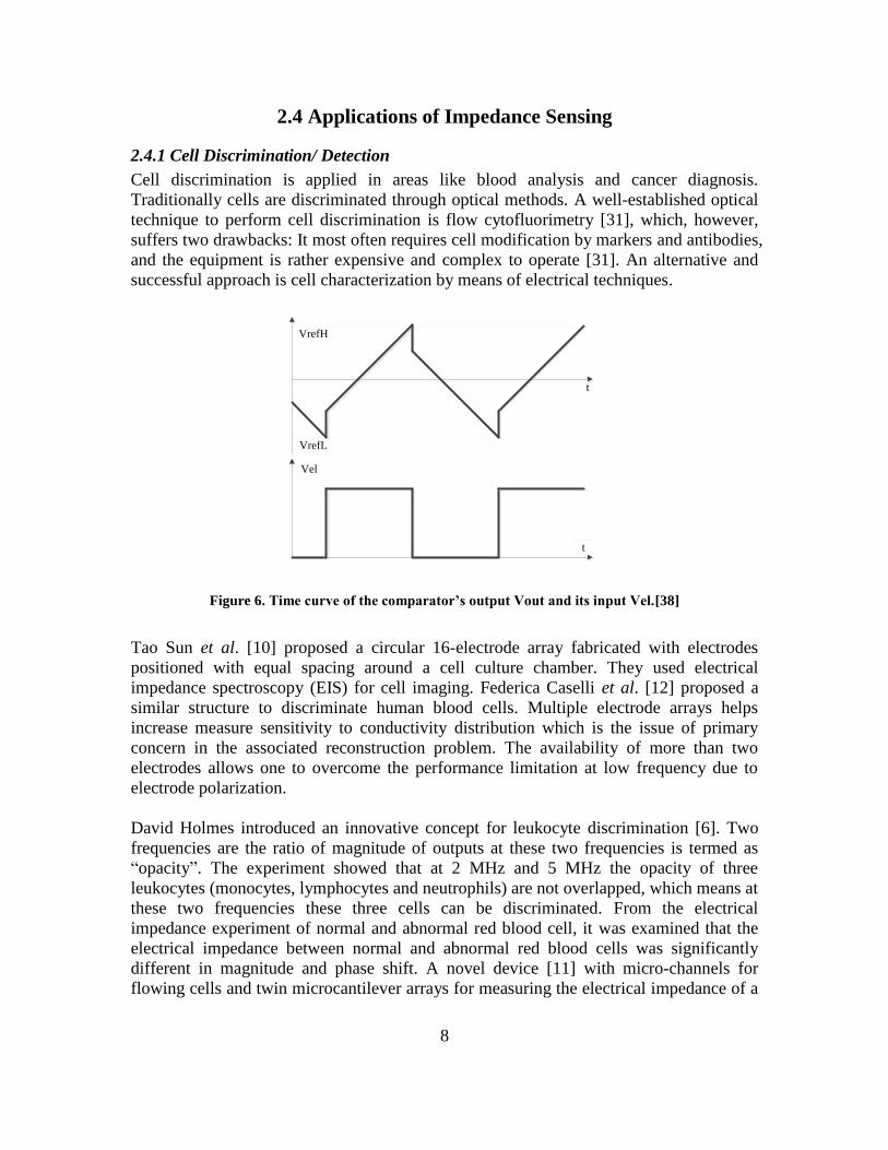
2.4.1 Cell Discrimination/ Detection
Cell discrimination is applied in areas like blood analysis and cancer diagnosis.
Traditionally cells are discriminated through optical methods. A well-established optical
technique to perform cell discrimination is flow cytofluorimetry [31], which, however,
suffers two drawbacks: It most often requires cell modification by markers and antibodies,
and the equipment is rather expensive and complex to operate [31]. An alternative and
successful approach is cell characterization by means of electrical techniques.
t
VrefH
VrefL
t
Vel
Figure 6. Time curve of the comparator’s output Vout and its input Vel.[38]
Tao Sun et al. [10] proposed a circular 16-electrode array fabricated with electrodes
positioned with equal spacing around a cell culture chamber. They used electrical
impedance spectroscopy (EIS) for cell imaging. Federica Caselli et al. [12] proposed a
similar structure to discriminate human blood cells. Multiple electrode arrays helps
increase measure sensitivity to conductivity distribution which is the issue of primary
concern in the associated reconstruction problem. The availability of more than two
electrodes allows one to overcome the performance limitation at low frequency due to
electrode polarization.
David Holmes introduced an innovative concept for leukocyte discrimination [6]. Two
frequencies are the ratio of magnitude of outputs at these two frequencies is termed as
“opacity”. The experiment showed that at 2 MHz and 5 MHz the opacity of three
leukocytes (monocytes, lymphocytes and neutrophils) are not overlapped, which means at
these two frequencies these three cells can be discriminated. From the electrical
impedance experiment of normal and abnormal red blood cell, it was examined that the
electrical impedance between normal and abnormal red blood cells was significantly
different in magnitude and phase shift. A novel device [11] with micro-channels for
flowing cells and twin microcantilever arrays for measuring the electrical impedance of a

9
single cell show that the normal cell can be taken apart from the abnormal cell by
electrical impedance measurement. The data shows distinct differences in the impedance
properties of leukocyte subpopulations at specific frequencies. A micro-EIS (MEIS)
system has the ability to differentiate cells based on cellular properties associated with
the plasma membrane and the intracellular contents [39-42]. This allows for detection of
abnormal cells as well as classification of normal cell types. Due to the sensitivity of the
measurement in response to the relative position of a cell between the impedance
measurement probes, positioning the target cell precisely at a desired location is
important. A microsystem that can manipulate and trap a single cell precisely between the
impedance measurement electrodes has been developed and used for characterizing ion
channel activities of single cells [43, 44].
Rc
Cm
Cm
Oscilloscope
Figure 7. working principle of the microfluidic cell cytometry[32]
2.4.2 Cell Counting
David Holmes et al. fabricated an innovative device [11] for label-free single-cell
leukocyte counting by impedance sensing. Differential signals were applied to reduce
noise and create a pair of positive and negative peaks for cell counting. S.Gawad et al.
proposed a device [31] for cell counting and separation in hematology, oncology or
toxicology. In the experiment, human erythrocytes and erythrocyte ghost cells (contents
of cell removed) were measured. When a single cell passes the electrodes, it will generate
a current peak which reflects its impedance. The impedance of the ghost cells was
smaller than the normal cells. Based on the number of the current peaks, they were able
to obtain the ratio of the normal cells to the ghost cells.

10
2.4.3 Cell Viability
An impedance-to-frequency converter [45] was proposed to monitor the viability of
human lung cells. The output frequency was proportional to the impedance, which
represents the coverage of cells over the electrodes. The output frequency was an
indicator which was related to the value of impedance. The system can easily be
integrated with digital-signal-processing circuits on chip, because only a counter is
needed.
Electric cell-substrate impedance sensing (ECIS) was used for monitoring the progression
of cytopathic effect (CPE) due to influenza a virus infection [14]. The entire system was
obtained from Applied Biophysics. This system included an impedance test control
module, an array station and culture wells at the bottom of which gold electrodes are
mounted. Evangelia Hondroulis, et al. [36] designed an array-formatted whole cell based
electrical impedance sensing system (EIS) that is able to show the kinetic effects of gold
or silver nanoparticles single walled carbon nanotubes (SWCNTs) and cadmium oxide
(CdO) when in contact with CCL-153 and RTgill-W1 cells. It measures the impedance of
a monolayer of cells cultured on the surface of electrodes. This system was compact, easy
to use, and capable of measuring multiple samples simultaneously in real time. Gold
electrodes were used in fabrication of the sensor arrays. Wilson Roa et al. [46] used real-
time cell-impedance sensing (RT-CES) system (ACEA Biosciences, San Diego, CA,
USA) to measure the impedance of cells to evaluate cancer radiotherapy [47].
2.5 Electrodes Design for the Impedance Sensing
S. Gawad et al. [31] measured the differential variation of impedance ZAC – ZBC as the
cell passes consecutively into two successive channel segments shown in Figure 8.
A B C
Figure 8. Side schematic view of the micro-channel
Figure 8 shows the side schematic view of the microchannel showing a particle passing
over three electrodes (A, B and C). The impedance signal is measured differentially (ZAC

11
– ZBC). Hydrodynamic focusing is used to center the particle in the channel. (b)
Impedance signal. As the distance between the two measurement areas and time ttr
separating the signal spikes are known, the speed of the particle can be calculated. In this
type of sequential differential sensor the reference and measurement electrodes are
inherently switched, revealing uneven drift of electrode properties. The innovative design
includes two arrays of electrodes instead of just two pairs of coplanar or parallel-facing
electrodes. The availability of more than two electrodes allows one to overcome the
performance limitation at low frequency due to electrode polarization. .
Meinrad Schienle et al. [48] presented a single sensor consists of interdigitated gold
working electrodes. Electrode width and spacing are 1 μm, total sensor diameter is 250
μm. The chip was realized in a 5V, 0.5μm, 2 metal CMOS process extended with extra
process steps to form gold sensor electrodes [49]. The chip occupies 6.4 mm × 4.5 mm.
The electrical behavior of the chip is characterized for a specified range of currents
between 1 pA and 100 nA. In a test mode, these currents are forced into the circuits via a
test input using an external current source. The electrode proposed by Xiaoqiu Huang et
al. [9] is 50 μm × 50 μm, which is small enough to monitor behaviors of single cells. The
electrode arrays were fabricated in standard CMOS process.
2.6 Challenges of Cell Impedance Sensing and Potential Solutions
2.6.1 Long-Term Monitoring
A high-density sensor array complementary metal-oxide-semiconductor (CMOS) chip [8]
is presented with 16,000 pixels, a frame rate of 2 kiloframes per second and a pitch of 7.8
μm × 7.8 μm for imaging of neural activity. A mismatch-canceling calibration circuitry
with current mode signal representation is used. Total area 6.5 mm × 5.2 mm.
Recording the activity of neural networks has always been a central goal in neurobiology
and is gaining importance in cell-based pharma screening. Compared to traditional ways,
the advantage of using a high-density electrode array to detect the motion of neurons is
its high throughput and suitability for long-term monitoring. Using an electrode array
makes it suitable to detect neuron network, which means it can monitor a group of
neurons in parallel. The design of this electrode array chip is based on the fact that the
action potentials to be considered correspond to sodium and potassium ion currents
through ion channels in the cell membrane. Consequently, the idea behind these
approaches is to monitor these ion currents instead of the transmembrane voltage.
H.R. Siddiquei et al. [15] cultured DF-1 cells (derived from chicken embryonic
fibroblasts, CEF cells) in Dulbecco’s Modification of Eagle’s Medium (DMEM) media.
The cells’ growth rate was monitored over a period of 3 days by continuous impedance
measurements using an impedance analyzer. This measuring method provides several
advantages: (i) it is less time consuming compared to conventional methods, (ii) it is
possible to automate and quantify cell morphology measurements, and (iii) the
fluctuating impedance pattern can be used as signature for a cell [50].

12
2.6.2 Real-time Monitoring
Real time monitoring of live cells in lab-on-chip systems has proven useful in various
applications [2, 31, 46, 51]. In pharmaceutical research, it allows, for example, an
effective screening of new drug candidates, thus reducing costs and the number of
necessary animal experiments. Another promising application is the detection of
environmental toxins, where mammal or even human-derived cell lines make highly
sensitive yet broadband indicators for substances that could harm man or animal [45].
2.6.3 High Throughput Readout
A micromachined impedance spectroscopy flow cytometer [31] measured the spectral
impedance of individual cells or particles and allows screening rates over 100 samples
per second on a single-cell basis. Instead of scanning the entire electrode array, the
approach presented here provides a reconfigurable electrode/readout-channel routing to
select an arbitrary subset of electrodes for recording and stimulation. This enables both,
low-noise signal recording, and cellular or subcellular resolution, since the front-end
circuitry can be placed outside the array, where sufficient area for a low-noise circuit
implementation is available. Special post-CMOS processing and packaging steps are
required to render the chip capable of operating in physiological solution with cell
cultures on top. The 2-mask post-processing step includes sputtering Ti:W (20 nm) as
adhesion and platinum (200 nm) as electrode materials and patterning of the metals with
the help of a lift-off process. The size of the chip is 7.5 × 6.1 mm, the size of the
electrode array is 2.0 × 1.75 mm.
Lim Lay Keng et al. [52] presented the CMOS implementation of a high throughput bio-
sensor array that consists of 96 × 96 electrodes. It is a single cell-based biosensor, which
is targeted to achieve both detection and identification of cell type. The magnitude and
phase of the cell impedance are measured from 100 Hz to 100 KHz. A grand challenge
for circulating cancer cell (CTC) detection technologies was formulated and published in
the Lab-on-a-chip journal in 2011. It proposed a multipoint addressable design with high
throughput electro-chemical detection [53].
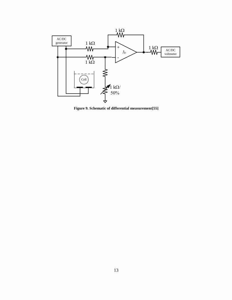
2.6.4 Improving Accuracy
The main design challenge of biosensors is to increase the SNR and DR while
minimizing the complexity of both the assay and the detector [54]. Differential
measurement is one solution to improve the accuracy. The solution resistance and the
surface capacitance are affected by ion concentration and temperature. Using differential
structure can reduce the measurement error results from these factors. [55]
13
AC/DC
generator
Cell
-
+A0
1 kW
1 kW
1 kW
1 kW/
50%
1 kWAC/DC
voltmeter
Figure 9. Schematic of differential measurement[55]

14
CHAPTER 3 INTEGRATED IMPEDANCE SENSING USING A
SILICON COCHLEA
Figure 10 shows the system diagram of an impedance sensor. AC voltage is applied
across the electrodes on the bottom of the culture well. When the cells are attached to the
electrodes, they block electric field generated by the voltage source, thus reducing the
current flowing through the electrodes. The impedance sensing circuits can detect this
change and obtain the cell impedance from it. The ramp ADC is used to transform the
output of the impedance sensing circuits to digital data which is easier to be stored in the
memory of the computer.
3.1 Silicon Cochlea based on Tau-cell in 0.5 μm process
The impedance sensing circuit can be the silicon cochlea, which is derived from the
biological cochlea. It is used for multi-frequency impedance sensing. The silicon cochlea
is composed of several series connected low pass filters. The filters have different cut-off
frequencies. The input signals are divided into several components of different
frequencies. These components are applied on the cells to obtain the impedance based on
Ohm’s law. There are two methods have already been used for impedance sensing: Fast
Fourier Transformation (FFT) and Frequency Response Analysis (FRA). Compared to
FFT, the silicon cochlea saves power because FFT needs to be implemented by the high
speed digital circuits. Compared to FRA, the silicon cochlea is more efficient because it
is able to measure the impedance at different frequencies simultaneously. Figure 10
shows the block diagram of the silicon cochlea. It is composed of four series connected
low pass filters. The cut-off frequencies are from 100 Hz to 100 kHz in logarithmic scale
because previous test results [5, 6] have shown that the human cancers cells have lower
impedance than the normal cells in this frequency span.
Impedance
Sensing
Circuits
Ramp ADC
Voltage
Source
Cell
Electrode
Culture Well
Figure 10. Block diagram of the impedance sensor

15
The low pass filters in the silicon cochlea are working in subthreshold reagion so it can
work in low voltage supply and saves some power. Tau-cell is used in this design,
because it is suitable for the synthesis of the subthreshold circuits. In this design, the filter
is composed of two cascaded tau-cells[56]. Figure 11 is the schematic of one tau-cell. Its
main structure is a translinear loop composed of four transistors M1, M2, M3 and M4. The
capacitor C and current I0 determines the time constant of the tau cell: i=CUT/ I0 where
UT is the thermal voltage (25.9 mV). Ii is the output current of this tau cell, while Ii+1 is
the output current of the next stage, Ii-1 is the output current of the tau cell before this
stage. Ai is the feedback coefficient of stage i, the feedback circuit is shown in .The
relationship of Ii-1, Ii and Ii+1 is:
1 11
i i i i i iI s A I A I
,
The transfer function of the tau cell is:
1 1
1
1
i
i
i i i i i
IT
I s A AT
where Ti+1 is the transfer function of the next stage. The transfer function of the filter is
the production of all the cascaded Tau cells [56]. In this design, the low-pass filters have
two cascaded Tau cells, the diagram is shown in Figure 15. In Figure 15, I2 is the output
of the filter. When 1 = 2, A1=2-1/Q, the transfer function of the two-order low-pass filter
based on Tau cell can be written as:
2 2
1
/ 1T
s s Q
,
The silicon cochlea is made up of 4 series-connected low-pass filter based on Tau-cell.
Figure 16 shows the block diagram of the silicon cochlea. The cut-off frequency of the
four filters are 100 kHz, 10 kHz, 1 kHz and 100 Hz. The cut-off frequency is determined
by the bias current Ibias and capacitors C1 and C2. The bias current and capacitors’ values
are shown in Table 1. Figure 17 shows the chip picture of the silicon cochlea in 0.5 m
process. The chip occupies 1.5 mm × 1.5 mm, and it has 40 pins. The voltage supply is 5
V.
Table 1. Bias current and capacitors of the filters in 0.5 m process.
Filter Cut-off frequency Ibias C1,2
Filter1 100 kHz 50 nA 100 fF
Filter2 10 kHz 2 nA 100 fF
Filter3 1 kHz 200 pA 100 fF
Filter4 100 Hz 20 pA 100 fF

16
Vref
Ii-1
AiI0
AiI0Ii+1/Ii
I0
2I0
Ii
M1 M2 M3 M4
Figure 11. Basic structure of a Tau-cell
100 kHz 10 kHz 1 kHz 100 Hz
I1 I2 I3
I4Iin
Figure 12. Block diagram of silicon cochlea
Vreff
AiI0Ii+1/Ii
AiI0
Ii+1
Ii
M1 M2 M3 M4
M5
Figure 13. The feedback circuit of the Tau-cell
1 2
IinI1 I2
A1
Figure 14. Block diagram of two-stage low-pass filter based on tau cells

17
Iin
Vref
Ibias
Iout1 Iout2
Vreff
Mn1 Mn2Mn3 Mn4 Mn5 Mn6 Mn7 Mn8
Mn9Mn10
Mn11 Mn12Mn13
Mn14Mn15
Mp1 Mp2 Mp3 Mp4 Mp5 Mp6
Mp7
Mp8
Mp9 Mp10 Mp11Mp12 Mp13
Mn16
C1 C2
Figure 15. Schematic of the Tau-cell based low pass filter
Table 2. Size of the Transistors of tau-cell.
Transistor Size
Mn1,2,3,4,5,6,8,11,12,13,14,15 12 m/12 m
Mn9,10 24 m / 12 m
Mn16 1.5 m / 12 m
Mp1 9 m / 12 m
Mp2 15 m / 12 m
Mp3,4 12 m / 12 m
Mp5 15 m / 12 m
Mp6 12 m / 12 m
Mp7,8 9 m / 12 m
Mp9,11 12 m / 12 m
Mp10 9 m / 12 m
Mp12,13 15 m / 12 m

18
filter1 filter2 filter3 filter4Iin
Vref
Vreff
Ib1 Ib2 Ib3 Ib4
Iout
Figure 16. Block diagram of the silicon cochlea
Figure 17. Photomicrograph of the silicon cochlea in 0.5 m process.
Table 3. Aspect ratio of the transistors in Figure 18.
Transistor Aspect Ratio
MP1,2 1.5 m/ 12 m
MN1-4, MN6-9, MN11-14, MN16-20,
MN15, MN17-20 1.5 m/ 12 m
MP3 3 m /12 m
MP4 12 m/ 12 m
MN5 6 m/12 m
MN10 30 m/12 m

19
Table 4. Bias current of the silicon cochlea in Figure 18.
Bias Current Value
Ib1 100 nA
Ib2 10 nA
Ib3 1 nA
Ib4 100 pA
Figure 18 shows the schematic of the bias circuit of the silicon cochlea. The bias current
of the filters in Figure 18 are shown in Table 4. The input bias current of the silicon
cochlea Ib is 100 pA. The bias current of the filters are obtain by amplifying Ib through
the current mirror. The channel length of the transistors in Figure 19 are 12 m which is a
big value compare to the feature length of 0.5 m process, so the channel length
modulation has little effect on the current mirror. There are four identical silicon cochleae
on the chip so that this chip can measure the impedance of four culture wells
simultaneously. The reference voltage Vref and Vreff are sued to make sure that the circuits
are working properly in the subthreshold region.
Five chips were fabricated for the test. They were numbered from 1 to 5. Chip No.3
didn’t work because the bonding wires might be broken when the chip was open to take
pictures of the layout. When testing, the SR785 signal analyzer provided a 20 mV input
signal. The sensitivity of SR570 current amplifier is 1 A/ V. Figure 19 to Figure 29
show the gain response and phase response of the four filters of the silicon cochlea chip
No.1, No.2, No.4 and No.5 respectively. The tested cut-off frequency of the four filters
and their expected cut-off frequency in the design are listed in Table 5.

20
filter1 filter2 filter3 filter4Iin
Vref
Vreff
Ib1 Ib2 Ib3 Ib4
Iout4
Silicon Cochlea 1
Silicon Cochlea 2
Silicon Cochlea 3
Iout1 Iout2 Iout3
VrefVreff
Iin1
Iin2
Iin3
Ib1 Ib2 Ib3 Ib4
Ib1 Ib2 Ib3 Ib4
Ib1 Ib2 Ib3 Ib4
MP1 MP2
MN1 MN2 MN3
MN4
MP3 MP4
MN5 MN6
MN7 MN8
MN9
MP5 MP6
MN10 MN11
MN12 MN13
MN14
MP7MP8
MP9
MN15 MN16 MN17
MN18
MN19
MN20
Figure 18. Silicon cochlea array with current bias
Table 5. Expected cut-off frequency and tested cut-off frequency of the filters in silicon cochlea on 0.5
μm process.
No of Chip No. of Filter Expected f-3db Tested f-3db
Chip 1 Filter 1 100 kHz 62.3 kHz
Filter 2 10 kHz 62.3 kHz
Filter 3 1 kHz 5.7 kHz
Filter 4 100 Hz 19.6 kHz
Chip 2 Filter 1 100 kHz 79.7 kHz
Filter 2 10 kHz 41.7 kHz
Filter 3 1 kHz 4.8 kHz
Filter 4 100 Hz 4.8 kHz
Chip 4 Filter 1 100 kHz 55.8 kHz
Filter 2 10 kHz 55.8 kHz
Filter 3 1 kHz 3.8 kHz
Filter 4 100 Hz 3.8 kHz
Chip 5 Filter 1 100 kHz 70.4 kHz
Filter 2 10 kHz 54 kHz
Filter 3 1 kHz 50.6 kHz
Filter 4 100 Hz 1.4 kHz

21
Figure 19. Frequency response of chip 2 channel 1, amplitude
Figure 20. Frequency response of chip 4, amplitude
Figure 21. Frequency response of chip 5, amplitude

22
Figure 22. Frequency response of chip 1 channel 2, amplitude
Figure 23. Frequency response of chip 1 channel 3, amplitude
Figure 24. Frequency response of chip2 channel 2, amplitude

23
Figure 25. Frequency response of chip 2 channel 3, amplitude
Figure 26. Frequency response of chip4 channel 2, amplitude
Figure 27. Frequency response of chip4 channel 3, amplitude

24
Figure 28. Frequency response of chip5 channel 2, amplitude
Figure 29. Frequency response of chip5 channel 3, amplitude
Figure 30. Test results of filter1 (cut off frequency supposed to be 100 kHz)

25
Figure 31. Monte Carlo simulation results of the filter 1
The cut-off frequency is the most important parameter to assess the performance of the
low pass filter in the silicon cochlea, because it determines the output accuracy of the
filters. There are four low pass filters in each silicon cochlea, and they are numbered. The
cut-off frequencies of the filters in the silicon cochlea are 100 kHz (Filter1), 10 kHz
(Filter2), 1 kHz (Filter3) and 100 Hz (Filter4). There are three identical silicon cochleae
on each chip, and four chips were tested, so there are 12 samples of each filter. The
measured cut-off frequencies of Filter1 are plotted as a histogram shown in Figure 30.
This histogram shows that most samples have a noticeable deviation to the desired value
(100 kHz). To make sure if the process variation and circuit mismatch are the reasons
cause the deviation, Monte Carlo simulation results are compared with the test results.
Test results of filter 1 show that the cut off frequency is mostly at 5 kHz, while the Monte
Carlo simulation result show that the cut off frequency is mostly at 80 kHz. This
difference means that besides process variation there are some other reasons cause the
deviation of the cut off frequency. Further research shows that the parasitic capacitance
is the main factor that cause the decrease of the cut off frequency. Table 6 to Table 8
show the average value and standard deviation of the cut off frequencies of the filters
from test results and Monte Carlo simulation. Simulation results have also shown that
process variation has more effect on the deviation of the cut off frequency.
3.2 Silicon Cochlea Design in a 130 nm Process
We designed the silicon cochlea in a 6 metal 1 poly 130 nm process. The schematic of the
Tau-cell in Figure 33 is almost the same as the in the 0.5 m process, the sizes of the
transistors are different. Table 9 shows the sizes of the transistors in the tau-cell based
filter. The only difference is the bias current is sinking instead of draining.

26
The structure of the silicon cochlea in 130 nm is the same as that in 0.5 µm, which is
shown in Figure 2. Table 10 shows the bias current, cut-off frequency and load capacitor
of the filters in the 130 nm process.
Figure 34 shows the frequency response of silicon cochlea (chip 4) in 130 nm process.
The cut off frequency of filter 1, 2, 4 are supposed to be 100 kHz, 10 kHz, and 100 Hz,
respectively. Table 11 shows the expected cut-off frequencies of the filters and the tested
values. Test results show that since the parasitic capacitors are considered, the
performance of the silicon cochlea in 130 nm is better than that in 0.5 m process. The
cut off frequency of filter 2 is much larger than the desired value, this is because of the
current mirror’s channel length modulation.
Figure 32. Monte Carlo simulation of filter1 with 8.34 pF load
Table 6. Average value and standard deviation of the cut off frequency from the test results.
Filter Average/ Hz Standard Deviation/ Hz
Filter1 32.6k 27.5k
Filter2 29.7k 22.4k
Filter3 19.3k 25.3k
Filter4 15.9k 18.6k
Table 7. Monte Carlo simulation of the filters with parasitic capacitors (only circuit mismatch is
considered).
Filter Average/ Hz Standard Deviation/ Hz
Filter1 1.68k 421
Filter2 2.29k 713.5
Filter3 782.4 45.6
Filter4 71.3 9.5

27
Table 8. Monte Carlo simulation of the filters with parasitic capacitors (only process variation is
considered).
Filter Average/ Hz Standard Deviation/ Hz
Filter1 1.62k 409.5
Filter2 2.23k 677.3
Filter3 737.3 396.2
Filter4 66.3 52.4
Iin
Vref
Ibias
Iout1 Iout2
Vreff
Mn1 Mn2Mn3 Mn4 Mn5 Mn6 Mn7 Mn8
Mn9Mn10
Mn11 Mn12Mn13
Mn14
Mn15
Mp1 Mp2 Mp3 Mp4 Mp5 Mp6
Mp7
Mp8
Mp9 Mp10 Mp11Mp12
Mn16
C1 C2
Mn16
Figure 33. Schematic of Tau-cell in 0.13 m process
Table 9. Sizes of the transistors in 130 nm process
Transistor Size
Mn1,2,3,4,5,6,8,11,12,13,14 2.4 m/ 2.4 m
Mn9,10 4.8 m / 2.4 m
Mn15 2.4m/ 2.4 m
Mn16 0.6 m / 2.4 m
Mp1 1.8 m / 2.4 m
Mp2 3 m / 2.4 m
Mp3,4 2.4 m / 2.4 m

28
Mp5 3 m / 2.4 m
Mp6 2.4 m / 2.4 m
Mp7,8 1.8 m / 2.4 m
Mp9,11 2.4 m / 2.4 m
Mp10 1.8 m / 2.4 m
Mp12 3 m / 2.4 m
Table 10. Cut-off frequency, bias current and load capacitors of the filters in 8RF.
Filter Cut-off frequency Ibias C1,2
Filter1 100 kHz 1.2 nA 153 fF
Filter2 10 kHz 1.2 nA 2.6 pF
Filter3 1k Hz 120 pA 21.3 pF
Filter4 100 Hz 2 pA 53.3 pF
Table 11. Expected cut-off frequency and tested cut-off frequency of the filters in the silicon cochlea.
No of Chip No. of Filter Expected f-3db Tested f-3db
Chip 4 Filter 1 100 kHz 68 kHz
Filter 2 10 kHz 55 kHz
Filter 3 1 kHz No Data
Filter 4 100 Hz 100 Hz
Figure 34. Phase response of the filters on chip 3 in 130 nm process

29
CHAPTER 4 CURRENT MODE INTEGRATED IMPEDANCE
SENSING
*Portions of this chapter originally published as:
J. Gu and N. McFarlane, "A low power multi-frequency current mode lock-in amplifier
for impedance sensing," IEEE International Instrumentation and Measurement
Technology Conference, Pisa, pp. 494-499, 2015.
J. Gu and N. McFarlane, "Low power current mode ramp ADC for multi-frequency cell
impedance measurement," IEEE International Midwest Symposium on Circuits and
Systems, Boise, ID, pp. 1016-1019, 2012.
4.1 On-chip Lock-in Amplifier
The lock in amplifier (LIA) is an instrument for measuring the reactance i.e. both the real
and the imaginary parts of the impedance. Measuring the cell impedance is useful for
cancer diagnosis, because biomedical research has proved that the tumor cells have lower
impedance than the normal cells. There has been some previous work on cell impedance
sensing. ECIS is a method to measure impedance and capacitance of the cell layer.
Previous work has shown that the cell impedance can be measured by a lock-in amplifier
with multi electrode arrays.
Fast and portable cancer diagnosis requires incorporating the ECIS system onto a silicon
IC chip, because the commercial LIA is bulky and costly. On chip LIAs will make
biomedical analysis easier and cheaper.
There has been some work on the silicon LIAs [57-60]. However, all of them are in
voltage mode. It is difficult for them to obtain the magnitude and phase of the input
signal in analog domain because it is difficult to implement pytharogator and arctangent
circuits in voltage mode. Consequently, most impedance sensing systems require digital
signal processing (DSP) modules to calculate the magnitude and the phase from the
outputs of the LIA which are in-phase and quadrate-phase components. In this thesis, we
propose a current-mode LIA which can calculate the magnitude and phase of the input
signal directly. This structure saves power and chip area because digital signal processing
(DSP) module is not needed in this proposed structure.
The LIA has four channels. Each channel has two sub-channels, one is for measuring the
real part of the impedance, and the other one is for the imaginary part. Each channel
contains a mixer and a low pass filter. The bandpass filter and phase shifter are used to
generate the LO signals. The transconductors are used to transfer the voltage into current.
The pytharogator obtains the magnitude of the impedance, while the divider obtains the
tangent of the impedance. The phase of the impedance is derived from the arctangent of
the divider output.

30
The cutoff frequency of the four channels are different, so that the LIA can measure the
impedance of the cells at different frequency simultaneously. The frequency resolution is
dictated by the frequency divided by the number of channels.
The mixer of the LIA is a 4-Quadrant current mode multiplier. It is derived from a 2-
Quadrant multiplier. In the test, the inputs are generated from on-chip transconductors.
Those transconductors are composed of an OPAMP, a single MOS transistor and a
resistor. One input AC signal is transferred into two differential AC current. The mixer is
in current mode, while the signal generator in the lab are in voltage mode. So the off
transconductors are made on vector board for generating the current input for testing the
mixer. Figure 37 shows the schematic of the transconductor, and Table 12 . The efficient
number of bits (ENOB) is a parameter to assess the output accuracy of the LIA. When
designing a LIA, the mixer’s performance determined the accuracy of the LIA. Previous
research [5, 14] has shown that in order to tell the difference between the normal cells
and the cancer cells, the ENOB of the LIA show be above 5 bits.
Table 13 shows the measured ENOB of the mixer. The test results show that the mixer’s
performance has achieved the requirement for cell discrimination.
Impedance
Sensing
Circuits
Impedance
Sensing
CircuitsRamp ADC
Figure 35. System diagram of the cell impedance sensor with readout circuits

31
2 2X Y
Y
X
Electro
de
Biomol
ecule
arctan(j)
r1
j1
Gm
Gm90o
-
+A0
Electro
de
LIA Channel
Channel 2
Channel 4
r2
j2
r4
j4
Figure 36 Block diagram of the lock-in amplifier
VDD
I1 I1
I2
I2
I3
I3
I4
MP1 MP2
MN1 MN2
MN3 MN4
MP3 MP4
MP5MP6
MP11MP12
MP7 MP8
MP9 MP10
Figure 37. Schematic of the 4-Q mixer in the LIA
Table 12. Transistor size of the 4-Q mixer.
Transistor Size
MP1,2,3,4 6 m/ 1 m
MP5~12 20 m/ 2 m
MN1,2,3,4 3 m/ 1 m

32
Table 13. Efficient number of bits (ENOB) of the mixer.
Frequency/ Hz ENOB/ bits
100 k 5.94
10 k 5.40
1 k 5.40
100 6.32
The divider is derived from 2-Q translinear multiplier. Four pmos transistors form a
translinear loop, and the aspect ratio of the transistors are 20 m/ 2 m. The divider
obtains the tangent of the phase by making IY divided by IX. The circuit is the same as the
2-quadrant multiplier in figure 6. I1 = IY, I2 = 1 nA, I3 = IX, so the output is:
1 24
3
I II
I ,
2
3
cosX
AI
I ,
2
3
sinY
AI
I ,
92 tan 1 10 tanoutI I ,
This output signal will be transformed into after the arctangent circuit.
Figure 38. Layout picture of the lock-in amplifier

33
I2
I1
I3
I4
Figure 39. Schematic of the 2-Q multiplier[61]
Figure 40. Output current of the 2Q multiplier versus Iin2
Figure 41. Output current of the 2Q multiplier versus Iin3

34
Figure 42. Frequency response of the LPF in the LIA
The LIA was designed in a 0.18 m process. There were five chips tested. The multiplier
was tested by sweeping input current Iin2 and Iin3. DC sweep test result showed that the
output current Io is in positive ratio to Iin3, which is in consistence to the simulation
results. Io shows a random response to Iin2, but according to the equation, the output
current should also be in positive ratio to Iin2. The reason that causes this difference is
unknown, but could be due to process variations and layout.
A current mode bandpass filter is used in this design. The transfer function of a 2-order
bandpass filter is:
2 2 1
sQ
H s
s sQ
,
The bandpass filter cannot be synthesized directly, so a 2-order low pass filter and a 1-
order low pass filter are used to generate a bandpass filter. Figure 43. Block diagram of
the 2-order MITE based bandpass filter shows the block diagram of the 2-order multiple
input translinear element (MITE) filter. The equation of the synthesis is shown below:
2 2
2 1 1 1 12 2 2 2
1
1 1
s s s Q sQ Q
X X Y X X
s s s sQ Q
,
2 2 2
2 2 2 21 2 1
11
11 1
s Q s sY Y X Q Q
X X X Q ss s s s
Q Q
,
Figure 44 shows the schematic of the bandpass filter. Its output is connected to the input
of the multiplier in Figure 39, so that the DC current of the bandpass filter is the same as
that of the multiplier, which is 32 nA. In order to ensure the filter is working in weak
inversion, the aspect ratios of all the PMOS transistors in the bandpass filter are 40 m/3
m. The aspect ratios of all the NMOS transistors are 24 m/3 m.

35
2 2
1
1s sQ
+
-X1
1
1Q s
Y1X2 Y2
Figure 43. Block diagram of the 2-order MITE based bandpass filter
IIN
VBIAS
VOUT
IOUT
IBIAS
Figure 44. The schematic of the 2-order MITE based banpass filter

36
100
101
102
103
104
105
106
107
-150
-100
-50
0
Frequency (Hz)
Gai
n (
dB
)
Post-layout
Pre-layout
Test Result
100
101
102
103
104
105
106
107
-150
-100
-50
0
Frequency (Hz)
Gai
n (
dB
)
Post-layout
Pre-layout
Test Result
100
101
102
103
104
105
106
107
-150
-100
-50
0
Frequency (Hz)
Gai
n (
dB
)
Post-layout
Pre-layout
Test Result
(a) (b) (c)
Figure 45. Experimental test result, pre-layout and post-layout simulation result of (a) bandpass
filter 100 kHz (b) bandpass filter 10 kHz, (c) bandpass filter 1 kHz
4.2 Ramp ADC
Overview of the Architecture of Current-Mode Ramp ADC
Our goal is to design a 10-bit low power, multi-channel current ramp ADC with a
sampling rate of 200 KHz. The figure below shows the block diagram of the current
mode ramp ADC. The main modules comprise a current ramp generator, current
comparator, delay lock loop (DLL) and counter. A two-step conversion technique is used
in this ADC. The digital counter is used for coarse conversion, while the DLL is used for
fine conversion. When the input current is sampled and added to the input of comparator,
the ramp generator begins to work. The comparators are then used to compare the input
signals with the current provided by ramp generator. When the output of the ramp
generator becomes larger than the input signal, the comparator’s output changes from low
to high, which will trigger the memory to record the output of the counter at that time.
The output of counter is not consistent with the output of ramp generator, so the digital
value recorded by the memory is the result of coarse conversion of ADC. The fine
conversion is accomplished by DLL. In the next section we discuss in detail the design of
the current mode ramp generator and current mode comparator.
Current Mode Ramp Generator
Figure 47 shows the schematic of the current mode ramp generator. In the integration
phase, the input current source is charging the capacitor at the input of operational
amplifier. As the input voltage of operational amplifier increases, the output current
increases accordingly. In the Figure 47, the channel length of the current mirror is large
enough so that Early effect can be neglected. The output current of ramp generator may
be given by:
g
or
S
II t
CR ,

37
where Ior is the output current of ramp generator, Ig is the input current, C is the capacitor
connected to the input of the operational amplifier (opamp), RS is the resistor connected
to the source follower and t is the time. IS is decided by the amplitude of the silicon
cochlea output currents. The value of C, RS and Ig depends on the trade-off between the
power consumed and the chip area. The capacitor is implemented on chip, it should
therefore not occupy too large an area. The capacitor is chosen to be 1 pF based on these
design considerations. Ig is provided by a bandgap reference source. In order to save
power, we do not want a large input current, so Ig is chosen to be 20 nA.. The output of
comparator changes from low to high when Iin crosses 15 μA. Iin = Ior – Ioc , where Ioc is
the amplified ourput current of silicon cochlea, Ior is the output of ramp generator. Ioc is a
constant value ranges from 0 to 10 μA in each integration period, so we need to make Ior
increase from 15 μA to 25 μA. A Cascode current mirror is used to increase the linearity
of ramp generator. Since the ramp generator needs to drive multiple comparators, it has
multiple outputs.
Current Mode Comparator
Figure 48 shows the low power high speed comparator used in this ADC. When the input
current increases to a certain value, the comparator’s output will change from 0 to Vdd.
Positive feedback increases the charging speed and gain of current amplifier. The resistor
improves matching in the current mirror. The aspect ratio of transistors M1-M4
determine the current gain, and R0 is used for reducing the DC offset. Transistors M9 to
M12 comprise two inverters. These inverters are used to ensure the output signal can
achieve rail-to-rail quickly.
Iin1
Iin2
Iinn
Counter
CLK
Memory
DLL
-
+
Ramp Generator
Channel n
Channel 1
Channel 2
Figure 46. Block diagram of the ramp ADC

38
-
+A0
Ior
Ig=20 nA
C=1pF
RS=10 KΩ
15.36 μm
0.96 μm
9.6 μm
0.24 μm
X
15.36 μm
0.96 μm
15.36 μm
0.96 μm
15.36 μm
0.96 μm
Vbias
Figure 47. Schematic of ramp generator
Iin
M1
M2
M3
M4
M5
M6
M7
M8
M9
M10
M11
M12
R0
Figure 48. Schematic of current comparator

39
Gray Code Counter
A Gray code counter is used for coarse conversion in this design. The advantage of Gray
code counter is that only one digit of its output will change in each clock period. This
prevents logic competition and adventure which causes the circuit receiving the output of
counter to go through states that are out of Gray code sequence. There are 2 D flip-flops
in each stage. This counter is only composed of feed-forward stages. The flip-flops are
divided into two groups. The upper group works as T flip-flops with XOR gates, while
the lower group is used for generating gray codes. It is a partly synchronous counter.
Ripple of this counter is smaller than traditional gray-code counters, because of its
synchronous operation. The rate of change in upper bits is reduced in this structure. This
structure also reduces the number of logic gates and power consumption.
D Q
QN
CLK
RESETSET
D0 D1 D2 D3
D D DQ Q Q
CLK CLK CLKQN QN QN
D Q
QN
CLK
D Q
QN
CLK
D Q
QN
CLK
D Q
QN
CLK
Figure 49. Schematic of a 4-bit Gray code counter[62]
Delay Locked Loop
In our design, the sampling rate is 200 KHz. For a traditional 10-bit ramp ADC, if the
sampling rate is 200 KHz, the clock frequency of the counter, fCLK is 210×200 KHz, which
is approximately 205 MHz. The circuit will consume a lot of power when it is working at
that high frequency. In our design, we want to keep the power consumption as low as
possible, because we are designing an ADC for an impedance sensing chip which will be
driven by battery (i.e. portable). A technique has been proposed and used in this design to
loosen the limit of sampling rate. The delay locked loop (DLL) is used to reduce the
number of bits in the counter, so that the clock frequency required by the counter can be
reduced.
The DLL is composed of two channels, channel A, channel B, and a phase detector.
Channel A consists of a group of inverters. Channel B consists of a group of inverters
connected with a D flip flop. The outputs of the inverters in group A are the results of
fine conversion. If the comparator produces a rising edge which will trigger the memory
between the counter counts n-1 and n (0< n < 210), the outputs of DLL will also be
recorded. The delay time of the inverters are controlled by the phase detector so the
output of the DLL will be synchronous with the output of the digital counter.

40
The main advantage of the DLL is that it does not work until the comparator’s output
changes from low to high, which saves the power of the chip. The DLL begins to
propagate this high signal through the inverter chain with a time interval 1/(m+p)fclk,
where m is the number of inverters in channel A and p is the number of inverters in
channel B. The number m determines the factor of clock frequency we can reduce. The
choice of m depends on the trade of stability of DLL and the power we want to save.
Based on this tradeoff, m is equal to 32 in our design. The clock frequency of our ADC
will be reduced from 205 MHz to 6.4 MHz.
Test Results of the Ramp Generator:
The ramp generator in the ADC was fabricated in 130 nm process and tested. Figure 50
shows the test setup for the ramp generator. The circuit in the dashed area is the ramp
generator on the chip. The switches are used to control the charging and discharging of
the integration capacitor Cint. When the Cint is charging, the output of the ramp generator.
This output Ior is compared with the reference input Iref of the comparator. When Ior
becomes larger than Iref, the comparator will generate a rising pulse to stop the counter
and store the output of counter into the memory. The MCP6024 in Figure 50 is a
commercial amplifier used as a buffer, because the output of the ramp generator will be
affected seriously by the parasitic components from the pads and package.
The output of the ramp generator is measured when it is in charging period. Figure 51
shows the curve of Ior versus time when the switch is controlled by a clock signal, the
rising edge of the curve is compared with the ideal curve to get the linear error of the
ramp generator. The linearity error is shown in Figure 52.
g
or
S
II t
CR ,
where Ig is the input current, C is the capacitor connected to the input of the operational
amplifier (opamp), RS is the resistor connected to the source follower and t is the time.
The input range of the 10-bit ramp ADC is 85 μA, so the LSB is 0.083 μA. The
maximum error of the ramp generator is 0.6 μA. The effective resolution is about 7 bits.
-
+A0
Ior
Cint
RS=10 kΩ
X
Vbias
-
+ Vor
RL=10 kΩ
MCP6024
Figure 50. Test setup of the ramp generator

41
Figure 51. Tested rising edge of Ior and the ideal Ior
Figure 52. Linearity error of the ramp generator

42
CHAPTER 5 CONCLUSION AND FUTURE WORK
In this thesis, two CMOS circuit architectures are proposed for cell impedance
measurement. The silicon cochlea and the lock in amplifier (LIA) are designed to
measure the impedance at different frequencies simultaneously. The silicon cochlea
connected to the ramp ADC can obtain the magnitude of the cell impedance, while the
LIA can obtain both the magnitude and the phase of the impedance.
The silicon cochlea is designed to measure the cell impedance. The silicon cochlea
designed in this work is composed of series connected 2-order low pass filters. These
filters are based on tau-cell in sub-threshold mode. The cutoff frequencies of the filters
are in logarithmic scale from 100 kHz to 100 Hz. The silicon cochlea transfer the input
signal into several sinusoidal signals. Two silicon cochleae are needed for cell impedance
measurement. One is for analyzing the current flowing through the cells, another one is
for generating the reference frequency. The silicon cochlea is designed and fabricated in
0.5 µm and 0.13 µm process. Monte Carlo simulation results showed the circuit
mismatch only contributes 10% of the frequency deviation of the filters, while the
process variation causes much more deviation the circuit mismatch. The test results
showed that the cutoff frequency of the 100 kHz and 10 kHz filter are reduced to below
10 kHz because of the parasitic capacitors.
The ramp ADC was designed for multi-frequency impedance sensing. The silicon
cochlea has four channels to measure the impedance at four frequencies simultaneously.
The simulation results show that the ramp generator and the capacitor has achieved 10 bit
accuracy. The test results show that the resolution of the ramp ADC is 7 bit, suitable for
the required application.
An innovative low-power multi-frequency on-chip LIA was also proposed. It measures
the complex impedance directly in analog domain and does not require a DSP module as
traditional LIAs do. Results show a power consumption of 207.7 W, with the largest
magnitude deviation being less than 7 %, and the largest phase deviation less than 4%.
Monte Carlo simulation shows the LIA’s mismatch is acceptable in 80% of the cases.
The core of the LIA system, the bandpass filters were fabricated and experimental
spectrums show excellent agreement with simulated results.
To summarize, the novel contributions of this thesis included:
1. Design of a silicon cochlea based impedance measurement system in a 0.5µm and
130nm process.
2. Design of a current mode lock-in amplifier in a 180nm process.
3. Design of a ramp ADC in a 180nm process.

43
Future Paths
There are many possible future paths to extend this thesis work. Future work could
include the design of high Q filters to improve the accuracy of the impedance
measurement. The arctangent circuit can be implemented as a polynomial function by
using Taylor approximation, where the polynomial function could be implemented by
multiple input translinear circuits. The concept of applying information theoretic models
to quantify tradeoffs could be applied to include noise sources and to optimize the
impedance sensing circuits described in this thesis.

44
LIST OF REFERENCE

45
[1] J. R. MacDonald, "Impedence Spectroscopy--Emphasizing Solid Materials and
Systems," Wiley-Interscience, John Wiley and Sons, pp. 1-346, 1987.
[2] L. Bousse, "Whole cell biosensors," Sensors and Actuators B: Chemical, vol. 34,
pp. 270-275, 1996.
[3] A. D. Marcellis, G. Ferri, P. Mantenuto, and A. D. Amico, "A new single-chip
analog lock-in amplifier with automatic phase and frequency tuning for
physical/chemical noisy phenomena detection," in 5th IEEE International
Workshop on Advances in Sensors and Interfaces (IWASI),, 2013, pp. 121-124.
[4] J. R. Macdonald, "Impedance spectroscopy," Annals of Biomedical Engineering,
vol. 20, pp. 289-305.
[5] A. Han, L. Yang, and A. B. Frazier, "Quantification of the heterogeneity in breast
cancer cell lines using whole-cell impedance spectroscopy," Clin Cancer Res, vol.
13, pp. 139-43, Jan 1 2007.
[6] Y. Cho, H. S. Kim, A. B. Frazier, Z. G. Chen, D. M. Shin, and A. Han, "Whole-
Cell Impedance Analysis for Highly and Poorly Metastatic Cancer Cells," Journal
of Microelectromechanical Systems, vol. 18, pp. 808-817, 2009.
[7] Y. YeoHeung, D. Zhongyun, N. S. Vesselin, and J. S. Mark, "Electrochemical
impedance measurement of prostate cancer cells using carbon nanotube array
electrodes in a microfluidic channel," Nanotechnology, vol. 18, p. 465505, 2007.
[8] B. Eversmann, M. Jenkner, F. Hofmann, C. Paulus, R. Brederlow, B. Holzapfl, et
al., "A 128 × 128 CMOS biosensor array for extracellular recording of
neural activity," IEEE Journal of Solid-State Circuits, vol. 38, pp. 2306-2317,
2003.
[9] H. Xiaoqiu, I. Nausieda, D. W. Greve, M. M. Domach, and D. Nguyen,
"Development of active matrix biosensor array for cell screening," in IEEE
Proceedings of Sensors, 2004, pp. 72-75 vol.1.
[10] S. T. Tao Sun, Klause-Peter Zauner and Hywel Morgan, "Singel Cell Imaging
Using Electrical Impedance Tomography," presented at the IEEE International
Conference on Nano/Micro Engineered and Molecular Systems, Shenzhen, China,
2009.
[11] D. Holmes, T. Sun, H. Morgan, J. Holloway, J. Cakebread, and D. Davies,
"Label-Free Differential Leukocyte Counts Using a Microfabricated, Single-Cell
Impedance Spectrometer," in Sensors, 2007 IEEE, 2007, pp. 1452-1455.
[12] P. B. a. F. M. Federica Caselli, "EIT-Inspired Microfluidic Cytometer Single-Cell
Dielectric Spectroscopy," Journal of Microelectromechanical Systems, vol. 19,
2010.
[13] J. Wegener, C. R. Keese, and I. Giaever, "Electric Cell–Substrate Impedance
Sensing (ECIS) as a Noninvasive Means to Monitor the Kinetics of Cell
Spreading to Artificial Surfaces," Experimental Cell Research, vol. 259, pp. 158-
166, 8/25/ 2000.
[14] M. H. McCoy and E. Wang, "Use of electric cell-substrate impedance sensing as a
tool for quantifying cytopathic effect in influenza A virus infected MDCK cells in
real-time," Journal of Virological Methods, vol. 130, pp. 157-161, 12// 2005.
[15] H. R. Siddiquei, A. N. Nordin, M. I. Ibrahimy, M. A. Arifin, N. H. Sulong, M.
Mel, et al., "Electrical cell-substrate impedance sensing (ECIS) based biosensor

46
for characterization of DF-1 cells," in Computer and Communication Engineering
(ICCCE), 2010 International Conference on, 2010, pp. 1-4.
[16] M. Brischwein, S. Herrmann, W. Vonau, F. Berthold, H. Grothe, E. R. Motrescu,
et al., "Electric cell-substrate impedance sensing with screen printed electrode
structures," Lab Chip, vol. 6, pp. 819-22, Jun 2006.
[17] A. W. Partin, J. T. Isaacs, B. Treiger, and D. S. Coffey, "Early cell motility
changes associated with an increase in metastatic ability in rat prostatic cancer
cells transfected with the v-Harvey-ras oncogene," Cancer research, vol. 48, pp.
6050-6053, 1988.
[18] T. B. Jones and T. B. Jones, Electromechanics of particles: Cambridge University
Press, 2005.
[19] N. G. Green, A. Ramos, and H. Morgan, "Ac electrokinetics: a survey of sub-
micrometre particle dynamics," Journal of Physics D: Applied Physics, vol. 33, p.
632, 2000.
[20] H. Morgan, T. Sun, D. Holmes, S. Gawad, and N. G. Green, "Single cell dielectric
spectroscopy," Journal of Physics D: Applied Physics, vol. 40, p. 61, 2006.
[21] F. F. Becker, X.-B. Wang, Y. Huang, R. Pethig, J. Vykoukal, and P. Gascoyne,
"Separation of human breast cancer cells from blood by differential dielectric
affinity," Proceedings of the National Academy of Sciences, vol. 92, pp. 860-864,
1995.
[22] P. Mitra, C. R. Keese, and I. Giaever, "Electric measurements can be used to
monitor the attachment and spreading of cells in tissue culture," Biotechniques,
vol. 11, pp. 504-510, 1991.
[23] I. Giaever and C. R. Keese, "A morphological biosensor for mammalian cells,"
Nature, vol. 366, pp. 591-592, 1993.
[24] C. R. Keese, J. Wegener, S. R. Walker, and I. Giaever, "Electrical wound-healing
assay for cells in vitro," Proceedings of the National Academy of Sciences of the
United States of America, vol. 101, pp. 1554-1559, 2004.
[25] C.-M. Lo, C. R. Keese, and I. Giaever, "Monitoring motion of confluent cells in
tissue culture," Experimental cell research, vol. 204, pp. 102-109, 1993.
[26] D. A. Lauffenburger and A. F. Horwitz, "Cell migration: a physically integrated
molecular process," Cell, vol. 84, pp. 359-369, 1996.
[27] E. A. Vogler, "Thermodynamics of short-term cell adhesion in vitro," Biophysical
journal, vol. 53, p. 759, 1988.
[28] W. Parak, J. Domke, M. George, A. Kardinal, M. Radmacher, H. Gaub, et al.,
"Electrically excitable normal rat kidney fibroblasts: a new model system for cell-
semiconductor hybrids," Biophysical journal, vol. 76, pp. 1659-1667, 1999.
[29] J. P. Nolan and L. A. Sklar, "Suspension array technology: evolution of the flat-
array paradigm," TRENDS in Biotechnology, vol. 20, pp. 9-12, 2002.
[30] H. M. Davey and D. B. Kell, "Flow cytometry and cell sorting of heterogeneous
microbial populations: the importance of single-cell analyses," Microbiological
reviews, vol. 60, pp. 641-696, 1996.
[31] S. Gawad, L. Schild, and P. Renaud, "Micromachined impedance spectroscopy
flow cytometer for cell analysis and particle sizing," Lab on a Chip, vol. 1, pp.
76-82, 2001.

47
[32] T. Sun and H. Morgan, "Single-cell microfluidic impedance cytometry: a review,"
Microfluidics and Nanofluidics, vol. 8, pp. 423-443, 2010.
[33] K. Mohri, T. Uchiyama, L. P. Shen, Y. Honkura, M. Yamamoto, and L. V.
Panina, "Amorphous wire & CMOS IC based sensitive micro magnetic
sensors utilizing magneto-impedance (MI) and stress-impedance (SI) effects," in
IEEE International Digest of Technical Papers, 2002, p. DC6.
[34] F. Lin, M. McKnight, J. Dieffenderfer, E. Whitmire, T. Ghosh, and A. Bozkurt,
"Microfabricated impedance sensors for concurrent tactile, biopotential, and
wetness detection," in IEEE SENSORS Proceedings, 2014, pp. 1312-1315.
[35] S. N. Nihtianov, G. P. Shterev, B. Iliev, and G. C. M. Meijer, "An interface circuit
for R-C impedance sensors with a relaxation oscillator," IEEE Transactions on
Instrumentation and Measurement, vol. 50, pp. 1563-1567, 2001.
[36] K. Mars and S. Kawahito, "Low-noise readout circuits with a response time
acceleration technique for high output impedance sensors," in IEEE Asia Pacific
Conference on Circuits and Systems (APCCAS), 2010, pp. 1159-1162.
[37] P. Vooka and B. George, "A Direct Digital Readout Circuit for Impedance
Sensors," IEEE Transactions on Instrumentation and Measurement, vol. 64, pp.
902-912, 2015.
[38] A. Mucha, M. Schienle, and D. Schmitt-Landsiedel, "A CMOS integrated
impedance-to-frequency converter for sensing cellular adhesion," Advances in
Radio Science, vol. 9, pp. 281-287, 2011.
[39] S. Gawad, K. Cheung, U. Seger, A. Bertsch, and P. Renaud, "Dielectric
spectroscopy in a micromachined flow cytometer: theoretical and practical
considerations," Lab on a Chip, vol. 4, pp. 241-251, 2004.
[40] Y. Huang, N. Chen, J. Borninski, and B. Rubinsky, "A novel microfluidic cell-
chip for single cell analysis and manipulation," in IEEE The Sixteenth Annual
International Conference on Micro Electro Mechanical Systems, 2003, pp. 403-
406.
[41] R. Go, R. Bashir, A. Sarikaya, M. Ladisch, J. Sturgis, J. Robinson, et al.,
"Microfluidic biochip for impedance spectroscopy of biological species,"
Biomedical Microdevices, vol. 3, pp. 201-209, 2001.
[42] H. M. Shapiro, "The evolution of cytometers," Cytometry Part A, vol. 58, pp. 13-
20, 2004.
[43] A. Han, E. Moss, R. D. Rabbitt, and A. B. Frazier, "A multi-purpose micro
system for electrophysiological analyses of single cells," in Micro Total Analysis
Systems 2002, 2002, pp. 805-807.
[44] A. Han, E. Moss, R. D. Rabbitt, K. L. Engisch, and A. B. Frazier, "A single cell
multi-analysis system for electrophysiological studies," in 12th International
Conference on Transducers, Solid-State Sensors, Actuators and Microsystems,
2003, pp. 674-677.
[45] A. Mucha, M. Schienle, and D. Schmitt-Landsiedel, "Sensing cellular adhesion
with a CMOS integrated impedance-to-frequency converter," in IEEE Sensors
Applications Symposium (SAS), 2011, pp. 12-17.
[46] W. Roa, X. Yang, L. Guo, B. Huang, S. Khatibisepehr, S. Gabos, et al., "Real-
time cell-impedance sensing assay as an alternative to clonogenic assay in

48
evaluating cancer radiotherapy," Analytical and bioanalytical chemistry, vol. 400,
pp. 2003-2011, 2011.
[47] J. Z. Xing, L. Zhu, J. A. Jackson, S. Gabos, X.-J. Sun, X.-b. Wang, et al.,
"Dynamic monitoring of cytotoxicity on microelectronic sensors," Chemical
research in toxicology, vol. 18, pp. 154-161, 2005.
[48] M. Schienle, C. Paulus, A. Frey, F. Hofmann, B. Holzapfl, P. Schindler-Bauer, et
al., "A fully electronic DNA sensor with 128 positions and in-pixel A/D
conversion," IEEE Journal of Solid-State Circuits, vol. 39, pp. 2438-2445, 2004.
[49] F. Hofmann, A. Frey, B. Holzapfl, M. Schienle, C. Paulus, P. Schindler-Bauer, et
al., "Fully electronic DNA detection on a CMOS chip: device and process issues,"
in IEEE International Electron Devices Meeting, 2002, pp. 488-491.
[50] S. P. Mohanty, "Biosensors: A survey report," University of South Florida, USA,
2001.
[51] Y. Qiu, R. Liao, and X. Zhang, "Real-time monitoring primary cardiomyocyte
adhesion based on electrochemical impedance spectroscopy and electrical cell-
substrate impedance sensing," Analytical chemistry, vol. 80, pp. 990-996, 2008.
[52] L. L. Keng, A. Jalabert, and R. Weerasekera, "Design and implementation of a
bio sensor array (BSA) for cancer cell detection," in 13th International
Symposium on Integrated Circuits (ISIC), 2011, pp. 400-403.
[53] K. Ino, W. Saito, M. Koide, T. Umemura, H. Shiku, and T. Matsue, "Addressable
electrode array device with IDA electrodes for high-throughput detection," Lab on
a Chip, vol. 11, pp. 385-388, 2011.
[54] A. Manickam, A. Chevalier, M. McDermott, A. D. Ellington, and A. Hassibi, "A
CMOS electrochemical impedance spectroscopy (EIS) biosensor array," IEEE
Transactions on Biomedical Circuits and Systems, vol. 4, pp. 379-390, 2010.
[55] B. M. Byrne, Structural equation modeling with AMOS: Basic concepts,
applications, and programming: Routledge, 2013.
[56] A. v. Schaik and C. Jin, "The tau-cell: a new method for the implementation of
arbitrary differential equations," in International Symposium on the Proceedings
of Circuits and Systems, 2003, pp. I-569-I-572 vol.1.
[57] P. M. M. Hern, xe, ndez, M. T. S. Pascual, and B. Calvo, "Micropower CMOS
lock-in amplifier for portable applications," Electronics Letters, vol. 52, pp. 828-
830, 2016.
[58] M. R. Valero, N. Medrano, S. Celma, and B. Calvo, "A CMOS 1.2-V 1.7-mW
lock-in amplifier for sensing applications up to 0.7-MHz," in IEEE SENSORS
2014 Proceedings, 2014, pp. 78-81.
[59] A. Hu and V. P. Chodavarapu, "CMOS Optoelectronic Lock-In Amplifier With
Integrated Phototransistor Array," IEEE Transactions on Biomedical Circuits and
Systems, vol. 4, pp. 274-280, 2010.
[60] X. Jiawei, M. Guy, and P. Merken, "Low-power lock-in amplifier for complex
impedance measurement," in Advances in sensors and Interfaces, 2009. IWASI
2009. 3rd International Workshop on, 2009, pp. 110-114.
[61] A. Boura and M. Husak, "NMOS and PMOS Translinear Multiplying Cell for
Current-Mode Signal Processing," in International Conference on Advanced
Semiconductor Devices and Microsystems 2008, pp. 83-86.

49
[62] N. Nambiar, B. J. Blalock, and M. N. Ericson, "A current mode multi-channel
Wilkinson ADC," in IEEE International Conference on Signals and Electronic
Systems 2008, pp. 11-14.

50
VITA
Jinlong Gu was born on March 18th, 1984 in Shanghai, China. He received his bachelor’s
degree in microelectronics from Fudan University in 2006, and received a master’s
degree in the same university in 2009. The topic of his thesis wass “a 10-bit 110 MS/s
Pipeline ADC Design”. After graduation from Fudan University, he worked as a CMOS
IC design engineer from June 2009 to December 2010.
He entered the University of Tennessee as a graduate student in spring 2011. Under the
support of Dr. McFarlane, he has been working on CMOS translinear circuits for cell
impedance sensors. He has designed and tested a silicon cochlea, lock-in amplifier, and
ramp ADC. Additionally, he worked on quantifying the noise, power and input signal
characteristic using techniques from information theory and applied to perimeter gated
single photon avalanche diodes. He has published 2 conference and 1 journal papers in
the past 5 years. His research interest is in mixed signal CMOS integrated circuit design.