CMOS AND MEMS BASED MICROSYSTEMS FOR MANIPULATION …
134
UNIVERSITÉ DE MONTRÉAL CMOS AND MEMS BASED MICROSYSTEMS FOR MANIPULATION AND DETECTION OF MAGNETIC BEADS FOR BIOMEDICAL APPLICATIONS YUSHAN ZHENG DÉPARTEMENT DE GÉNIE ÉLECTRIQUE ÉCOLE POLYTECHNIQUE DE MONTRÉAL THÈSE PRÉSENTÉE EN VUE DE L’OBTENTION DU DIPLÔME DE PHILOSOPHIAE DOCTOR (GÉNIE ÉLECTRIQUE) NOVEMBRE 2014 © Yushan Zheng, 2014.
Transcript of CMOS AND MEMS BASED MICROSYSTEMS FOR MANIPULATION …
UNIVERSITÉ DE MONTRÉAL
CMOS AND MEMS BASED MICROSYSTEMS FOR MANIPULATION AND
DETECTION OF MAGNETIC BEADS FOR BIOMEDICAL APPLICATIONS
YUSHAN ZHENG
DÉPARTEMENT DE GÉNIE ÉLECTRIQUE
ÉCOLE POLYTECHNIQUE DE MONTRÉAL
THÈSE PRÉSENTÉE EN VUE DE L’OBTENTION
DU DIPLÔME DE PHILOSOPHIAE DOCTOR
(GÉNIE ÉLECTRIQUE)
NOVEMBRE 2014
© Yushan Zheng, 2014.

UNIVERSITÉ DE MONTRÉAL
ÉCOLE POLYTECHNIQUE DE MONTRÉAL
Cette thèse intitulée :
CMOS AND MEMS BASED MICROSYSTEMS FOR MANIPULATION AND DETECTION
OF MAGNETIC BEADS FOR BIOMEDICAL APPLICATIONS
présentée par : ZHENG Yushan
en vue de l’obtention du diplôme de : Philosophiae Doctor
a été dûment acceptée par le jury d’examen constitué de :
M. LAURIN Jean-Jacques, Ph. D., président
M. SAWAN Mohamad, Ph. D., membre et directeur de recherche
M. MARTEL Sylvain, Ph. D., membre
Mme TABRIZIAN Maryam, Ph. D., membre externe

iii
DEDICATION
To my family

iv
ACKNOWLEDGEMENTS
I would first like to thank my supervisor, Professor Mohamad Sawan for all his support,
encouragement and guidance during my Ph.D. research life in Polystim Neurotechnologies
Laboratory.
I would also like to thank Professor Jean-Jacques Laurin, Professor Sylvain Martel, and Professor
Pierre Haddad for their suggestions at the early stage of my Ph.D. research. Their resourceful
experience helped me get rid of some unnecessary detours in research.
Thanks are due to three intern students I guided, Sara Bekhiche, Abir Mannai and Cyril
Jacquemod, for their hard work to contribute to my research project.
I thank all staff members and colleagues of Polystim Lab who helped me during my stay in
Polytechnique Montreal. Special thanks are due to the following people for their helps and
collaborations: Marie-Yannick Laplante, Laurent Mouden, Rejean Lapage, Jean Bouchard, Arash
Moradi, Sami Hached, Saeid Hashemi, Faycal Mounaim, Amine Miled, Mohamed Zgaren, and
Nan Li.
I am also grateful for the support from the Canada Research Chair in Smart Medical Devices, the
Natural Sciences and Engineering Research Council of Canada, CMC Microsystems and the
scholarship from China Scholarship Council.
Finally, I want to express the deepest gratitude to my family for their love and encouragements
during my study.

v
RÉSUMÉ
Les micro et nano billes magnétiques dédiées à l'étiquetage des bio-particules attirent de plus en
plus d'intérêt dans de nombreuses applications environnementales et sanitaires, tels que l'analyse
de gènes, le transport des médicaments, la purification et l'immunologie. Les dimensions réduites
et la haute sensibilité des billes magnétiques rendent leurs manipulations à haute précision
possibles. Leur simplicité de suivi dans le milieu biologique et leur biocompatibilité permettent
d’effectuer des détections rapides et à haute sensibilité pour des applications in vivo et in vitro.
L'utilisation traditionnelle des billes magnétiques prend place dans un laboratoire se servant du
matériel encombrant et dispendieux. Avec le développement de la technologie de
microfabrication, des billes magnétiques peuvent être traitées dans un microsystème, plus
précisément, dans une structure laboratoire sur puce (LoC). La combinaison microfluidique et
microélectronique offre des possibilités d’autoévaluation, ce qui peut augmenter l'efficacité du
travail.
Cette thèse est orientée vers de nouvelles approches pour la manipulation et la détection de bio-
particules se servant de la technologie de microsystèmes basées sur des structures
microelectroniques et microfluidiques et en utilisant des marqueurs de billes magnétiques. Basé
sur un réseau de microbobines à la fois comme une source de champ magnétique et un capteur
inductif, le microsystème proposé est réalisé grâce à l'efficacité de fabrication de structures
CMOS-MEMS, ainsi que des circuits intégrés dédiés CMOS de haute performance afin d'obtenir
un rendement élevé de manipulation et de détection de billes magnétiques.
Plusieurs défis ont été analysés dans la mise en œuvre de ces microsystèmes et des solutions
correspondantes fournies. Plus précisément, la conception et la mise en œuvre d'une plate-forme
contrôlée en température en format portable sont d'abord présentées, dans un effort réalisé pour
résoudre la question de la chaleur par effet Joule lors de l'application du réseau de microbobines
comme une source de champ magnétique dédié à la manipulation de billes magnétiques. Une
plateforme similaire à cette dernière a été améliorée pour effectuer une analyse magnétique
immunologique, en ajoutant des circuits de détection par des billes magnétiques. De plus, des
IgG et anti-IgG de souris ont été utilisés dans des expériences pour vérifier les performances de
détection de la plateforme de microsystème proposé. En outre, un substrat de silicium intégrant
une structure MEMS et incorpore à la fois un microcanal microfluidique et un réseau de

vi
microbobines sur une seule puce a été conçu et fabriqué suivant l'analyse par éléments finis (FEA)
de résultats de simulation. Cette dernière structure a été testée à l'aide de bio-particules attachées
à des billes magnétiques. Cette structure monolithique est susceptible d'être utilisée pour des
applications in vivo.

vii
ABSTRACT
Magnetic micro/nano beads as labels of bio-particles have been attracting more and more interest
in many environmental and health applications, such as gene and drug delivery, purification, and
immunoassay. The miniature size and high sensitivity of magnetic bead allow accurate
manipulation, whereas its high distinguishability from biological background and
biocompatibility make fast and high sensitivity detection possible for in vitro and in vivo
applications. Traditional employment of magnetic beads is done in laboratory environment with
the assist of bulky and expensive equipment. Thanks to the development of microfabrication
technology, magnetic beads therefore can be handled on a microsystem, more specifically, a Lab-
on-Chip (LoC). The combination of microfluidics with microelectronics offers the possibility of
automatic analyses, which can liberate the labor and increase the efficiency.
This thesis focuses on new approaches for bio-particles manipulation and detection on
microelectronic/microfluidic hybrid microsystems using magnetic beads as labels. Based on
planar microcoil array as both magnetic field source and the front-end inductive sensor, the
proposed microsystems can take advantage of the massive producible CMOS/MEMS fabrication
process, as well as the customized high performance CMOS circuits, to achieve a high efficient
magnetic beads manipulation and a quantitative detection.
Several challenges in implementing such microsystems are analyzed and corresponding solutions
are provided. Specifically, the design and implementation of a temperature controllable LoC
platform in portable format is firstly presented, for the sake of resolving the Joule heat issue
when applying microcoil array as magnetic field source in magnetic beads manipulation. The
similar platform is then improved to be used for magnetic immunoassay, by adding magnetic
beads sensing circuits. Mouse IgG and anti-mouse IgG are employed in experiments to verify the
detection performance of the proposed microsystem platform. Additionally, a fully integrated
silicon substrate MEMS chip which integrates both microfluidic channel and microcoil array on a
single chip is designed and fabricated following the Finite Element Analysis (FEA) simulation
results and tested using bio-particles attached magnetic beads. This monolithic chip has the
potential to be applied for in vivo applications.

viii
TABLE OF CONTENTS
DEDICATION ...................................................................................................................... iii
ACKNOWLEDGEMENTS ...................................................................................................... iv
RÉSUMÉ ....................................................................................................................... v
ABSTRACT ..................................................................................................................... vii
TABLE OF CONTENTS ........................................................................................................ viii
LIST OF TABLES .................................................................................................................... xi
LIST OF FIGURES .................................................................................................................. xii
LIST OF ABBREVIATIONS .................................................................................................. xii
INTRODUCTION ...................................................................................................................... 1
Motivation .............................................................................................................................. 1
Research Objectives ............................................................................................................... 2
Research Contributions ........................................................................................................... 3
Thesis Organization ................................................................................................................ 5
CHAPTER 1 THEORETICAL FOUNDATIONS OF MAGNETIC BEADS
MANIPULATION AND DETECTION .................................................................................. 6
1.1 Superparamagnetic Beads ................................................................................................. 6
1.2 Forces on Magnetic Beads in Liquid ................................................................................ 9
1.3 Magnetic Field Generated by Planar Microcoil ............................................................. 10
1.4 Joule Heat Generated by Microcoil ................................................................................ 13
1.5 Magnetic Beads Detection .............................................................................................. 14
CHAPTER 2 STATE OF THE ART OF THE LAB-ON-CHIP MICROSYSTEMS
USING MAGNETIC BEADS ......................................................................................... 18

ix
2.1 Labeled and Non-labeled Manipulation and Detection of Bioparticles-A Comparison 18
2.2 Microsystems for Magnetic Beads Manipulation ........................................................... 20
2.3 Microsystems for Magnetic Beads Detection ................................................................. 26
2.3.1 GMR Sensor ............................................................................................................. 26
2.3.2 Hall Sensor ............................................................................................................... 28
2.3.3 NMR Sensor ............................................................................................................. 30
2.3.4 Inductance Detection Based Magnetic Sensor ......................................................... 32
2.4 Microsystems Packaging Techniques ............................................................................. 34
CHAPTER 3 A TEMPERATURE CONTROLLABLE PLATFORM FOR
MAGNETIC BEADS MANIPULATION ............................................................................... 39
3.1 Introduction .................................................................................................................... 39
3.2 Planar Microcoil Array Based Temperature-controllable Lab-on-Chip Platform .......... 40
3.2.1 Abstract .................................................................................................................... 40
3.2.2 Introduction .............................................................................................................. 40
3.2.3 Joule Heat Effect Analysis and Simulation ............................................................. 42
3.2.4 Current Supply Circuit ............................................................................................. 47
3.2.5 Device Architecture and Fabrication ....................................................................... 49
3.2.6 Experimental Results ............................................................................................... 52
3.2.7 Conclusion ............................................................................................................... 56
CHAPTER 4 A MICROSYSTEM FOR MAGNETIC IMMUNOASSAY BASED ON
PLANAR MICROCOIL ARRAY ........................................................................................... 57
4.1 Introduction .................................................................................................................... 57
4.2 A Microsystem for Magnetic Immunoassay Based on Planar Microcoil Array ............ 58
4.2.1 Abstract .................................................................................................................... 58
4.2.2 Introduction .............................................................................................................. 58

x
4.2.3 Microcoil Sensor ...................................................................................................... 62
4.2.4 Integrated CMOS Chip Design ................................................................................ 67
4.2.5 Microsystem Prototype and Experiments ................................................................ 75
4.2.6 Conclusion ............................................................................................................... 80
CHAPTER 5 A NOVEL BIO-MEMS CHIP FOR MAGNETIC BEADS APPLICATIONS .....
..................................................................................................................... 81
5.1 Introduction .................................................................................................................... 81
5.2 A BioMEMS Chip with Integrated Micro Electromagnet Array towards Bio-particles
Manipulation ......................................................................................................................... 82
5.2.1 Abstract .................................................................................................................... 82
5.2.2 Introduction .............................................................................................................. 82
5.2.3 Design and Fabrication ............................................................................................ 83
5.2.4 Controllable Magnetic Field by Microcoil Array .................................................... 87
5.2.5 Experiments ............................................................................................................. 91
5.2.6 Discussion ................................................................................................................ 94
5.2.7 Conclusion ............................................................................................................... 94
CHAPTER 6 GENERAL DISCUSSION ......................................................................... 96
CHAPTER 7 CONCLUSION ........................................................................................... 99
7.1 Conclusion ...................................................................................................................... 99
7.2 Recommendation for Future Work ............................................................................... 100
BIBLIOGRAPHY .................................................................................................................. 102

xi
LIST OF TABLES
Table 1 MATERIAL PARAMETERS FOR MODELLING AND SIMULATIONS ................... 43
Table 2 COMPARISON WITH STATE-OF-THE-ART RESEARCHES .................................... 94

xii
LIST OF FIGURES
Figure 1.1 Diagram of (a) a red blood cell, (b) a magnetotactic bacterium, (c) a cell with digested
magnetic nanoparticles, and (d) a cell with magnetic micro/nano particles attached to
the surface [9] ................................................................................................................. 6
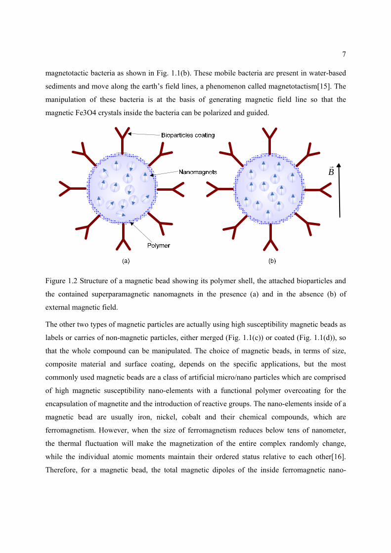
Figure 1.2 Structure of a magnetic bead showing its polymer shell, the attached bioparticles and
the contained superparamagnetic nanomagnets in the presence (a) and in the absence
(b) of external magnetic field. ......................................................................................... 7
Figure 1.3 Simplified schematic diagram of the main directions of the most important forces
acting on a magnetic bead. .............................................................................................. 9
Figure 1.4 Magnetic field generated by one loop of microcoil ...................................................... 11
Figure 1.5 (a)Planar spiral coil model: wire thickness 1um, inner diameter 60 µm, outer diameter
400um, and the current passing through the coil 100mA; (b) and its 3D model in FEA
software and the magnetic field distribution................................................................. 12
Figure 1.6 Magnitude of total magnetic flux density (a) along a line parallel to the surface of the
microcoil and located 20 µm above it; (b) along a line perpendicular to the surface of
the microcoil and located at the center of it. ................................................................. 12
Figure 1.7 Magnetic field distribution for different geometrical planar microcoils: a) planar coil
models, each coil occupies an area of 450 um by 450 um, carrying a current of 30 mA;
b) corresponding magnetic field distribution on the z = 1 um plane. ........................... 13
Figure 1.8 Planar microcoil for monitoring magnetic susceptibility: a) the microcoil and magnetic
particles with toxins captured; b) high frequency equivalent circuit model; c) cross
sectional view of a microcoil showing the magnetic field distribution. ....................... 15
Figure 2.1 Magnetic bead separator employing permanent magnets[54]. ..................................... 20
Figure 2.2 A microsystem combining permanent magnets and electromagnets. Cu current lines
are buried in the back side of the substrate at the positions indicated by the white lines.
...................................................................................................................................... 21
Figure 2.3 A summary of the performance of various planar electromagnets. Row 1: a schematic
view of the microcoil; row 2: image under optical microscope; row 3: the simulated

xiii
magnetic flux density profile; row 4: schematic of the magnetic bead trapping profile
and; row 5: optical image of the magnetic beads trapped by corresponding microcoils
[56] ................................................................................................................................ 22
Figure 2.4 (a) Schematic of the microsystem with the fluidic chamber on top of the coil and
pillar; (b) Prototype of final fluidic device with chip inserted in. The size of the fluidic
chamber is 10mm×5mm×0.1mm. The fluidic inlet and outlet, with inner diameter of
0.5 mm. The fluidic block is connected to a programmable syringe pump fitted with a
1 ml syringe[61]. ........................................................................................................... 23
Figure 2.5 Microcoil array for magnetic beads manipulation. By controlling currents in the
microcoils, many different magnetic field patterns can be generated. To generate the
required fields, current pulses with appropriate values and directions are alternatively
applied to two neighboring microcoils[62]. .................................................................. 24
Figure 2.6 An open cavity microsystem integrating CMOS coil array for individual magnetic
bead manipulation [51]. ................................................................................................ 25
Figure 2.7 Schematic of a GMR based magnetic flow sensor design [54] .................................... 27
Figure 2.8 A conceptual schematic view of a Hall sensor for single magnetic particle
detection[69]. An external magnetic field is applied to polarize the magnetic bead
which produces a stray magnetic field. ......................................................................... 29
Figure 2.9 Conceptual drawing of the NMR relaxometer and its proximity assay [59]. (a) The
bulk spin-spin relaxation time T2 for water molecules without test samples. (b) The
relaxation time is reduced with monodispersed magnetic particles. (c) The target
molecule i.e., proteins, trigger the proximity assay and lead to aggregation of magnetic
particles to form clusters, which further decrease the relaxation time of the water
molecules. ..................................................................................................................... 31
Figure 2.10 A microsystem for CMOS frequency-shift-based magnetic sensor array with
integrated microfluidic structures (left) and the zoom-in view of one differential
sensing pair (right) [59]. ............................................................................................... 32
Figure 2.11 Inductance detection based magnetic sensor for detecting DNA [64] ........................ 33
Figure 2.12 Application of PDMS in microfluidic chip [60] ......................................................... 35

xiv
Figure 2.13 Fabrication procedure of DWFP technique: (a) ink deposition, (b) encapsulation in
epoxy and (c) ink extraction [81]. ............................................................................... 36
Figure 2.14 A Sensonit glass substrate based hybrid microsystem[69]. ........................................ 37
Figure 3.1 Magnetic beads as solid phase carriers for bioparticles manipulation .......................... 41
Figure 3.2 The proposed closed-loop temperature control system. ............................................... 44
Figure 3.3 3D Model of microcoil with channel and substrate in CoventorWare: (a) complete
model; (b) Substrate is hidden to show microcoil array. .............................................. 44
Figure 3.4 Thermal propagation analysis when the input of a microcoil is constant-frequency
square-wave current. ..................................................................................................... 45
Figure 3.5 Maximum temperature variation for different current inputs: (a) DC input; (b)
Constant frequency input---duty cycle 1:2 and frequency 1Hz; (c) Variable frequency
input ---duty cycle 1:2 and frequency 1Hz from 0 to 2.75s; duty cycle 1:5 and
frequency 1Hz from 0 to 2.75s; duty cycle 1:5 and frequency 1 Hz after 2.75s. ......... 46
Figure 3.6 Schematic of the proposed bidirectional current source. .............................................. 48
Figure 3.7 Post layout simulation of bidirectional current supply circuit. ..................................... 49
Figure 3.8 Architecture of the microcoil array based LoC platform. ............................................. 50
Figure 3.9 The proposed polyimide substrate LoC device: (a) Hexagonal microcoil chip with
microfluidic structure; (b) Bottom view showing the heat dissipation layer and CMOS
chip; (c) Microphotograph of the CMOS chip; Die size 0.85mm by1.15mm; (d)
Square microcoil array. ................................................................................................. 50
Figure 3.10 Individual magnetic bead manipulated by two adjacent microcoil: (a)The targeted
observation area in the microcoil array; (b) Original position of the targeted magnetic
bead; (c) Magnetic bead was polarized and attracted toward the lower coil; (d)-(g)
Magnetic bead was attracted toward the upper microcoil. ........................................... 54
Figure 3.11 Mass beads trapping experiment showing the magnetic beads in solution
concentrated in the active coil region. .......................................................................... 55

xv
Figure 3.12 Monitored temperature variation during the whole magnetic beads trapping
experiment. ................................................................................................................... 55
Figure 4.1 Sensor network involving microsystem for monitoring environmental toxins. ........... 59
Figure 4.2 Flow chart for a typical magnetic immunoassay: a) antibodies are patterned on bottom
surface of substrate; b) under-test sample solution is introduced, specific antigens will
be captured due to antigen-antibody reaction, and other molecules in solution are
flushed out; c) magnetic beads labeled antibodies are injected, a sandwich structure is
formed. Superfluous beads that are not bound are flushed out. Finally the amount of
magnetic beads that can be detected by sensor reflects the amount of antigen. ........... 60
Figure 4.3 Main components of the proposed Magnetic Immunoassay microsystem. .................. 62
Figure 4.4 Planar microcoil as magnetic sensor: a) the concept of microcoil and magnetic
particles with toxins captured; b) high frequency equivalent circuit model; c) cross
sectional view of a microcoil showing the total magnetic field distribution; d) our
fabricated microcoil with inductance 210nH, DC resistance 0.65Ω and Q factor 75 at
200 MHz. ...................................................................................................................... 64
Figure 4.5 Block diagram of the achieved CMOS chip. ................................................................ 67
Figure 4.6 Schematic of cross coupled LC oscillator and self biased buffer circuit and simulation
results: a) schematic; b) transient simulation result; c) phase noise simulation results.
...................................................................................................................................... 69
Figure 4.7 Bidirectional multiple steps current supply circuit: a) schematic and b) post-layout
simulation result ............................................................................................................ 72
Figure 4.8 On-chip PTAT sensor circuit: a) schematic showing the temperature monitor and
control loop; b) simulation result. ................................................................................. 74
Figure 4.9 Prototype of the microsystem: a) The view of platform showing the setup of 96 wells
microplate, microcontroller board, LCD display and power supply circuits ; b) The
sensor board under the microplate; c) The backside view of sensor board showing the
mount of our designed CMOS chip; d)The micrograph of our designed CMOS chip. 76

xvi
Figure 4.10 Experiments results: a) real time data record showing output frequency v.s. time; b)
extracted data showing frequency shift v.s. density of mouse IgG. ............................. 77
Figure 4.11 Microscopic view showing the attached different densities of magnetic beads in
different microplate wells, the corresponding mouse IgG added in wells are: a)1ng/ml;
b)10ng/ml; c)100ng/ml; d)10ug/ml. ............................................................................. 79
Figure 5.1 Main fabrication flow used in this design: a) deposition and pattern of isolation oxide,
sacrifice oxide and nitride layer 1 and 2; b) deposition and pattern of metal layer(coil
structure), anchor metal layer(connection between polysilicon and metal) and
polysilicon layer; c) removal of oxide layer by HF solution to form the suspended
structure; d) KOH silicon etching to form the trench; e) top view of final device model
in Coventorware to show the whole device and microchannel. ................................... 86
Figure 5.2 Total magnetic field flux density distribution for different geometrical planar
microcoils: a) planar coil models, each coil occupies an area of 450 um by 450 um,
carrying a current of 30 mA; b) corresponding magnetic field distribution on the z = 1
um plane. ....................................................................................................................... 87
Figure 5.3 a) Total magnetic field flux density distribution on x-z plane where y=0; b) magnetic
flux density in x direction where z=25 µm. .................................................................. 88
Figure 5.4 Magnetic field distribution of coil array: a) Four-coil array model in Ansys. Width 8
um, space 8 um, outer diameter 450 um, inner diameter 80 um; b) applying current in
four coils with same amplitude and direction, mode AAAA; c) applying current with
same amplitude but opposite direction for adjacent coils, mode ABAB; d) applying
same amplitude current to four coils but with same direction in the top two and
opposite direction to the bottom two, mode AABB; e) x directional magnetic field
distribution, mode ABAB; f) z directional magnetic field distribution, mode ABAB.
(A and B represent the opposite current direction; figure b, c and d share the top
legend, whereas e and f share the bottom one). ............................................................ 90
Figure 5.5 Micrograph of MEMS chip: a) microcoil and bonding wires; b) inlet/outlet of
microfluidic; c) micropipette absorbing liquid containing magnetic particles; d)
micropipette dispensing liquid from inlet; e) magnetic particles near the outlet of
microchannel. ................................................................................................................ 92

xvii
Figure 5.6 Experimental results showing the normalized trapping ratios versus current
consumption for single, double and triple activated coil. Trapping ratio of 90% can be
achieved for triple coil regime while consuming a current of 40 mA. ......................... 93
Figure 7.1 Concept of an automated PCR chip with magnetic immunoassay for pathogens
detection. ..................................................................................................................... 100

xviii
LIST OF ABBREVIATIONS
LoC Lab on Chip
CMOS Complementary metal-oxide semiconductor
MEMS Micro electro-mechanical systems
PMOS P channel metal-oxide-semiconductor field effect transistors
NMOS N channel metal-oxide-semiconductor field effect transistors
FEA Finite Element Analysis
PoC Point of care
GMR Giant magnetoresistance
NMR Nuclear magnetic resonance
DC Direct current
AC Alternative current
DEP Dielectrophoresis
SPAD Single photon avalanche diode
MIA Magnetic immunoassay
PDMS Polydimethylsiloxane
EDA Electronic design automation
ELISA Enzyme-linked immunosorbent assay
PCB Printed circuit board
PTAT Proportional to absolute temperature
PCR Polymerase chain reaction
TDC Time to digital convertor
PLL Phase lock loop
ADC Analog to digital convertor

xix
MCU Micro control unit
MUX Multiplexier
DWFP Direct wirte fabrication process
µTAS Micro total analysis system
RT Room temperature

1
INTRODUCTION
Motivation
Microelectronic/microfluidic hybrid microsystems, as a branch of Lab on a Chip (LoC), has been
creating more and more interests in many application fields, including point of care (POC)
diagnostics, life science and environmental applications. These microsystems share the same
advantageous of LoC over the traditional macroscale in-lab methods, including compact size,
decreased reagent volumes, increased functionality, disposability, high throughput analyses.
Moreover, the combination of microfluidics with microelectronics offers the possibility of
turning the time-consuming and/or labor-intensive processes towards high efficient automated
analyses. Additionally, thanks to the development of microfabrication technology, many new
applications that are difficult to be realized in macro scale can be achieved on emerging hybrid
microsystems, because the interaction of microsystems with bioparticles opens a new window to
novel methods of medical diagnostics and environmental monitoring.
Various microsystems built by different mechanisms for bioparticles manipulation and detection
have been reported, such as mechanical structures based micro-tweezers for manipulation and
micro-cantilever for detection[1][2], electric field based dielectrophoresis (DEP) manipulation
and resistive/capacitive detection[3][4], magnetic field based magnetic beads labeled bioparticles
manipulation and detection[5][6], as well as optical field based light beam for manipulation and
fluorescence labeled bioparticles detection[7][8]. Among these microsystems, the ones using
magnetic micro/nano beads as labels of bioparticles have been attracting great attention in many
environmental and health applications, such as gene and drug delivery[9], purification[10], and
immunoassay[11]. As the labels of bioparticles, magnetic beads can be accurately manipulated
due to their miniature size and high magnetic susceptibility. Moreover, their high
distinguishability from biological background and their biocompatibility make fast and high
sensitivity detection possible for in vitro and in vivo applications.
Conventional devices for magnetic beads labeled bioparticles manipulation exploit external
ferromagnets or simple topological on-chip electromagnets for generating magnetic field, thus
they suffer from some drawbacks including low power efficiency, high cost, inaccurate
manipulation, and more difficulties for miniaturization. Therefore, the design of optimized on-

2
chip electromagnets for high efficiency and high flexibility manipulation are in demand.
Furthermore, in electromagnetic LoC applications, the inevitable Joule heating effect is widely
mentioned but usually treated by an additional complicated cooling system, which highly
increases the system complexity and total power consumption. In fact, it is possible to reduce the
Joule heat by improving the design of electromagnets and applying advanced control algorithms,
without increasing the complexity of hardware system design, thus the “overheating spot” issue
in conventional device can be avoided and the temperature of liquid can be always maintained
within the safe range to bioparticles.
Additionally, for the detection of bioparticles using magnetic beads as labels, despite a few
microsystems have been reported, there are several challenges yet to be overcome. The first is the
design of a high performance front-end magnetic sensor and its sensing circuits, which should
respect both sensitivity and linearity, for the sake of quantitative analysis. Moreover, many of the
conventional microsystems exploit expensive materials and non-standard fabrication process to
achieve the magnetic sensor, thus they are not suitable for large scale deployment for multiple
sites monitoring in environment or low cost PoC diagnostics. Furthermore, the packaging
technique is also very challenging because a robust biological interface will definitely facilitate
the device setup and testing process, thus shorter detection time and more reliable results can be
achieved.
Research Objectives
The main objective of this research is to study new approaches for bioparticles manipulation and
detection on microelectronic/microfluidic hybrid microsystems using magnetic beads as labels.
The detailed objectives are as follows:
• To design and fabricate planar microcoil array using mainstream microelectronic
fabrication processes for high efficiency magnetic beads manipulation
• To resolve the overheat spot issue caused by high current electromagnets, without
additional cooling system
• To be able to use the same microcoil array as both the magnetic field source for
manipulation and the front-end inductive sensor for detection

3
• To design high performance CMOS circuits to control microcoil array and to receive
sensing signal, in order to achieve a high efficient magnetic beads manipulation and a
quantitative detection
• To exploit a robust packaging technique for microfluidic/microelectronic hybrid
microsystem
• To test and verify the proposed microsystems using both artificial magnetic beads and
real bioparticles for practical use, for example, magnetic immunoassay.
• To explore new approach for miniaturization of microsystem by integrating microfluidic
structures and microelectronics on a single chip
Research Contributions
The contributions of this thesis are summarized as follows:
1\ Modeling, simulation and optimization of planar microcoil array with different geometries and
topologies by FEA software in order to optimize the magnetic field generated by microcoil, as
well as the magnetic force on magnetic beads by different controlling regimes of multiple coils,
thus different applications, such as trapping, separating, mixing and transporting, can be realized
at the highest efficiency in terms of power consumption.
2\The inevitable but often neglected Joule heat issue in electromagnetic LoC applications is
analyzed and proved to be controllable using our proposed current supply scheme. Microcoil can
be used as heat source to keep the temperature of whole microfluidic system within the safe range
for bioparticles, saving the external incubator. To verify the concept, a polyimide substrate LoC
platform is fabricated and tested using magnetic beads ranging from 1µm to 2µm.
The above contributions are detailed in our published articles:
• Yushan Zheng; Sawan, M., "Planar Microcoil Array Based Temperature-Controllable
Lab-on-Chip Platform," Magnetics, IEEE Transactions on, vol.49, no.10, pp.5236-5242,
Oct. 2013.
• Yushan Zheng; Bekhiche, S.; Sawan, M., "Planar microcoils array applied to magnetic
beads based lab-on-chip for high throughput applications," Circuits and Systems
(ISCAS), IEEE International Symposium on , pp.2345-2348, 15-18 May 2011.

4
3\ Circuit and system implementations of a novel microsystem platform for magnetic
immunoassay are presented. Three main challenges facing this work, design of a high
performance magnetic microcoil sensor, packaging technique and design of the sensing circuits
are discussed and corresponding solutions are provided. A complete magnetic immunoassay
experiment is performed using the proposed microsystem and results show that a fine detecting
sensitivity and linearity can be achieved thus the proposed platform is suitable for quantitative
analysis in medical diagnostics, food pathogen detection or water analysis.
The above contribution is reported in the following articles:
• Yushan Zheng; Jacquemod, C.; Sawan, M., "A portable lab-on-chip platform for
magnetic beads density measuring," Circuits and Systems (ISCAS), IEEE International
Symposium on , pp.1071-1074, 19-23 May 2013.
• Yushan Zheng; Sawan, M., "A microsystem for magnetic immunoassay towards protein
toxins detection," Circuits and Systems (ISCAS), IEEE International Symposium on ,
pp.225-228, 1-5 June 2014.
• Yushan Zheng; Shang, N.; Haddad, P.; Sawan, M. “A Microsystem for Magnetic
Immunoassay Based on Planar Microcoil Array,” Submitted to IEEE Transactions on
Biomedical Circuits and Systems.
4\ Design and fabrication of a novel BioMEMS chip towards the manipulation of magnetic
micro/nano particles is presented. The proposed monolithic chip integrates planar microcoil array
and microfluidic structure on a single chip, without any post-fabrication process. Meanwhile, a
multiple coil cooperation scheme is studied by simulation in FEA Software and applied in
experiment to increase the manipulation efficiency. Taking advantage of computer-aided
microplotter to introduce microfluidics to the chip, the traditional microtubes and syringe pump
are avoided. Hence, this chip is compact, low-cost and mass-producible.
More details can be found in the following article:
• Yushan Zheng, Abir Mannai, Mohamad Sawan, “A BioMEMS chip with integrated
micro electromagnet array towards bio-particles manipulation”, Microelectronic
Engineering, Vol. 128, 5 Oct. 2014, Pages 1-6.

5
Thesis Organization
The theoretical foundations of magnetic beads manipulation and detection are introduced in
Chapter 1, including the physical and biological properties of magnetic beads, forces on magnetic
beads in liquid, analysis of magnetic field generated by microcoil, Joule heat analysis, and
magnetic beads detection basis. A literature review on the state of the art microsystems for
magnetic beads manipulation and detection is discussed in Chapter 2, different types of
electromagnets for generating magnetic field and various magnetic biosensors are summarized
and compared. The design and implementation of a temperature controllable lab-on-chip platform
dedicated to resolving the overheat spot issue caused by big current in electromagnets is proposed
in Chapter 3, followed by the design and implementation of a microsystem for magnetic
immunoassay in Chapter 4, which includes also the design of a frequency shift magnetic
biosensor and its CMOS interface circuits. A monolithic bioMEMS chip integrated in a silicon
substrate is proposed in Chapter 5, with a microcoil array integrated on chip and a new method
for microfluidics handling, this chip achieves tubeless microfluidic processing. A general
discussion is conducted in Chapter 6, which summaries and discusses the whole thesis work.
Finally, the conclusions of thesis work, along with the recommendation for future work, are
presented in Chapter 7.

6
CHAPTER 1 THEORETICAL FOUNDATIONS OF MAGNETIC BEADS
MANIPULATION AND DETECTION
1.1 Superparamagnetic Beads
Depending on the behavior of the solid material under an external magnetic field, various types
of magnetism can be distinguished, such as diamagnetism(Au, Cu), paramagnetism(Pt, Mn),
ferromagnetism(Fe), ferrimagnetism(ferrite) and antiferromagnetism(Cr)[12], whereas magnetic
particles are referred to those micro/nano particles that can be manipulated using magnetic field.
Figure 1.1 Diagram of (a) a red blood cell, (b) a magnetotactic bacterium, (c) a cell with digested
magnetic nanoparticles, and (d) a cell with magnetic micro/nano particles attached to the surface
[9]
Usually there are four categories of magnetic particles employed in biomedical applications. The
first is a type of cells with intrinsic magnetic properties, for example, the deoxygenated red blood
cell (RBC), as shown in Fig. 1.1(a). Hemoglobin is the iron-containing oxygen-transport
metallo-protein in the RBCs of vertebrates[13]. In mammals, the protein makes up about 97% of
the RBC’s dry content, and around 35% of the total content (including water). Oxygenated RBCs
therefore have a small relative magnetic susceptibility with respect to that of water[14]. However,
this value is so small that only a magnetic field in tesla range can retain or separate RBCs. The
second type is another kind of magnetic cells existing in nature, which is usually called
7
magnetotactic bacteria as shown in Fig. 1.1(b). These mobile bacteria are present in water-based
sediments and move along the earth’s field lines, a phenomenon called magnetotactism[15]. The
manipulation of these bacteria is at the basis of generating magnetic field line so that the
magnetic Fe3O4 crystals inside the bacteria can be polarized and guided.
B
Figure 1.2 Structure of a magnetic bead showing its polymer shell, the attached bioparticles and
the contained superparamagnetic nanomagnets in the presence (a) and in the absence (b) of
external magnetic field.
The other two types of magnetic particles are actually using high susceptibility magnetic beads as
labels or carries of non-magnetic particles, either merged (Fig. 1.1(c)) or coated (Fig. 1.1(d)), so
that the whole compound can be manipulated. The choice of magnetic beads, in terms of size,
composite material and surface coating, depends on the specific applications, but the most
commonly used magnetic beads are a class of artificial micro/nano particles which are comprised
of high magnetic susceptibility nano-elements with a functional polymer overcoating for the
encapsulation of magnetite and the introduction of reactive groups. The nano-elements inside of a
magnetic bead are usually iron, nickel, cobalt and their chemical compounds, which are
ferromagnetism. However, when the size of ferromagnetism reduces below tens of nanometer,
the thermal fluctuation will make the magnetization of the entire complex randomly change,
while the individual atomic moments maintain their ordered status relative to each other[16].
Therefore, for a magnetic bead, the total magnetic dipoles of the inside ferromagnetic nano-

8
elements will be averaged to zero due to thermal fluctuation and the whole magnetic bead does
not exhibit magnetization in the absence of external field[17][18]; when an external magnetic
field is applied, the magnetic moments of the nano-elements will overcome the thermal
fluctuations and line up, thus the magnetic bead will exhibit a significant net magnetic moment as
illustrated in Fig. 1.2. Due to its similarity with paramagnetism but with much higher magnetic
susceptibility, this behavior is called superparamagnetism[19], and the beads that contain nano-
superparamagnetic nanoparticles are called superparamagnetic beads. This thesis employs such
superparamagnetic beads and uses the term “magnetic beads” for abbreviation. Compared with
other types of magnetic particles, for example torque-based Artificial Bacteria Flagella[20],
magnetic bead is chosen as carriers or labels or bioparticles because of higher magnetic
susceptibility and more flexible control. Usually, permanent magnets and big current
electromagnets can easily produce magnetic fields sufficiently strong to saturate the
magnetization of magnetic beads, making the beads behave simply as permanent magnets [21].
Magnetic bead can be prepared by encapsulating superparamagnetic nanoparticles inside of a
polymer shell as shown in Fig. 1.2. Polymer shell is used to isolate liquid from direct contact with
magnetic materials, and the amount of nanoparticles inside of a magnetic beads affect its size,
magnetic moment and surface to volume ratio[22]. Usually the increase of size results in the
decrease of surface to volume ration but higher magnetic moment. After the encapsulation of
magnetic bead, to attach the magnetic bead to bioparticles, the surface of the magnetic bead needs
to be chemically modified. This functionalized bead then can be bound to specific target
bioparticles. The preparation of functional magnetic beads with attached bioparticles for
biological and medical applications has been well studied and several reviews on this topic have
been reported[22][23]. In general, benefiting from large surface-to-volume ratio, such modified
particles can be advantageously used as solid phase or carrier for bio-assays, or even for in vivo
applications; they can be easily recovered from dispersion, reversibly re-dispersed; the
attachment and detachment usually are controlled by changing the some parameters of the
solution, such as temperature and pH. Nowadays, people can even purchase some well prepared
bioparticles attached magnetic beads from various companies and use them directly in
applications.

9
1.2 Forces on Magnetic Beads in Liquid
For a single magnetic bead in liquid, in addition to the magnetic force magF , it experiences
hydrodynamic drag force dragF , gravitational force and buoyancy force, while the latter two
forces can be considered as effective gravitational force gF as presented in Fig.1.3, and usually
neglected due to its small size.
magF dragF
gF
Figure 1.3 Simplified schematic diagram of the main directions of the most important forces
acting on a magnetic bead.
From Maxwell tensor equation, the force on a magnetic bead due to the applied magnetic field is
( )mag mF V H B= χ ⋅∇ (1)
where magF is the magnetic force on the bead, V is the volume of the bead, mχ is its magnetic
susceptibility per unit volume, H is the magnetic field intensity, and B is the magnetic flux
density, and “∇ ” is vector differential operator. Meanwhile, we know
B Hμ= (2)
where μ is the permeability of the medium.
In orthogonal coordinate system, extending Eq. (1) in x direction leads to
0
( )m x x xx x y z
V B B BF B B Bx y zμ
χ ∂ ∂ ∂= + +
∂ ∂ ∂ (3)

10
Eq. (3) indicates that the magnetic force acting on a bead depends on the magnetic field intensity,
as well as magnetic field gradient. That means a strong but uniform magnetic field may polarize
or even saturate magnetic beads, but only a non-uniform magnetic field with a significant
gradient will result in the movement of magnetic bead.
In addition to magnetic force, from Stokes’s law, we know the hydrodynamic force
6 ( )drag bead bead fluidF R v vπ= η − (4)
where beadv , fluidv , beadR and η are the bead velocity, liquid velocity, bead radius and fluid’s
viscosity, respectively. If we consider the case when beads are immobilized at the center of
microcoils, when we turn off the coil, magnetic bead will be forced to move along the flow
direction due to Eq. (4), at an initial velocity 0 and initial acceleration 6 /bead fluid beadR v mπη , where
beadm is the mass of a magnetic bead. Since in most microfluidic applications, fluidv is very small,
the acceleration is also very small, which means the beads will not escape from the coil center
area right away even if the magnetic force is removed in a short while.
For the manipulation of magnetic beads, the magnetic force on beads is required to be bigger than
hydrodynamic drag force, and a bigger magnetic force will result in a more sensitive controlling.
The magnetic field can be generated either by permanent magnets or electromagnets. The use of
permanent magnets offers advantage of strong magnetic field thus large magnetic force, but it
doesn’t allow flexible control of magnetic field, thus electromagnets are preferred, because the
intensity and directions of magnetic field can be easily controlled the current through
electromagnets.
1.3 Magnetic Field Generated by Planar Microcoil
Among various electromagnets, planar microcoil is usually preferred in LoC applications,
because of its low cost and compatibility with layer based microelectronic fabrication technology.
A spiral microcoil of multi-turn can be considered to be composed of an equal number of
concentric loops of different lengths, the total magnetic field is the sum of the magnetic field
induced by each loop, and it can be obtained from the Biot-Savart’s law as shown in Fig. 1.4:

11
02
ˆ4
Idl rB dBr
μπ
×= = ⋅∫ ∫ (5)
where 0μ is the magnetic constant; I is the current passing through wire; dl is a vector whose
magnitude is the length of the differential element of the wire, and whose direction is the
direction of current; r is the displacement unit vector, in the direction pointing from the wire
element to the point at which the field is being computed and r is the distance from the wire
element to the point at which the field is being computed.
Figure 1.4 Magnetic field generated by one loop of microcoil
Eq. (5) reveals that, approximately, for certain positions in space, the magnetic flux density
generated by a coil is directly proportional to the current through the coil and inversely
proportional to the distance from the investigated position to the coil. As the size of coil shrinks,
it need less and less current to generate the required magnitude of magnetic field within the coil’s
layout region. Hence, it can be concluded that following the minimum allowed metal width of
specific fabrication process to design the coil will result in strongest magnetic field in the coil
layout region.
Take the spiral microcoil as shown in Fig. 1.5 as an example: it is modeled in FEA software, with
wire thickness of 1um, inner diameter of 60 µm, outer diameter of 400um, and the current
passing through the coil of 100mA. FEA simulation results of the magnetic flux density versus
horizontal direction and vertical direction are shown in Fig. 1.6. When the center of the coil is
recognized as the origin, it is found that the magnetic flux density is almost symmetric both in x-
direction and z-direction, and the magnitude of magnetic field drops quickly as the distance to the

12
coil’s centre increases, which means both the maxima of magnetic flux density and magnetic
field gradient are located in the vicinity of this coil’s center.
Figure 1.5 (a)Planar spiral coil model: wire thickness 1um, inner diameter 60 µm, outer diameter
400um, and the current passing through the coil 100mA; (b) and its 3D model in FEA software
and the magnetic field distribution.
Figure 1.6 Magnitude of total magnetic flux density (a) along a line parallel to the surface of the
microcoil and located 20 µm above it; (b) along a line perpendicular to the surface of the
microcoil and located at the center of it.

13
However, the above feature is not always true when the topology of microcoil varies, because the
magnetic field distribution is highly geometry dependent. In a given area and consuming same
current, different geometries could lead to different maximum values of magnetic field as well as
their distribution. Since magnetic beads always tend to be attracted to the nearest maxima of
magnetic field, the distribution of trapped magnetic beads can be estimated through investigating
the geometries of planar microcoils. For example, as indicated in Fig. 1.7, coil 2&4 have their
maximum magnetic field at the center with large gradient, whereas coil 1&3 don’t have their
maximum magnetic field at the center but exert relatively more uniform magnetic field. In some
applications, for example trapping, magnetic beads are required to be trapped on the substrate
surface uniformly, instead of attracting all the magnetic beads to the center to form cluster, so the
design of coil 1 or 3 to achieve a more uniform and larger trapping area is more preferred. From
Fig. 1.7, it’s also found that the maximum magnetic field in coil 1&3 are lower than that in coil
2&4, therefore realizing a more uniform magnetic field is at the cost of higher current
consumption as a higher current is needed to reach the same magnetic force to manipulate the
magnetic beads.
Figure 1.7 Magnetic field distribution for different geometrical planar microcoils: a) planar coil
models, each coil occupies an area of 450 um by 450 um, carrying a current of 30 mA; b)
corresponding magnetic field distribution on the z = 1 um plane.
1.4 Joule Heat Generated by Microcoil
One inevitable but often neglected issue in electromagnet based LoC applications is Joule heat
effect. The heat may damage the viability of bioparticles, because most of the bioparticles can

14
only keep vital in a relatively narrow temperature range. Therefore, the heat generated by
microcoils has to be controllable. For a working microcoil, the induced Joule heat is
R=JQ JJ (6)
where R is the DC resistance and J is the current density. The parabolic equation of temperature conduction is expressed [24] as
ˆ ( ) [ ( )]T
q c T T Tt
ρ∂
= −∇ ∇∂
Ki (7)
where T is the temperature, ρ is the density, c(T) is the specific heat which might depend on the
temperature, K(T) is a conductivity matrix which might be orthotropic or temperature dependant,
and q is the heat generation rate per unit volume.
Eq. (6) and eq. (7) illustrate that a typical heating process can be recognized as two separate
phases: the first is the heat generation, whereas the second is heat conduction. The topology of
microcoil array influences the resistance and current density, thus affects the first process; the
parameters of substrate and the medium affect the second because different materials have
different specific heat and conductivities. If a DC current is applied to a microcoil, the heat
generation process dominates the heating dissipation process, so the maximum temperature keeps
rising. When the current is cut off, since there is no heating source any more, the heating
dissipation process will dominate and the temperature of microcoil will tend to return to ambient
temperature. Some previous studies used on-chip water cycling system or external thermoelectric
cooler to keep temperature stable in channel, which are proved effective in holding temperature,
but prior to these passive action, it is better to explore some more economic means to control
Joule heat by means of novel design concept or operation scheme, which will be elaborated in
Chapter 3.
1.5 Magnetic Beads Detection
In addition to using microcoil as magnetic field source to manipulate magnetic beads, the same
microcoil can be used as biosensor to detect the magnetic beads. The detection of magnetic beads
relies on the planar microcoil to sense the susceptibility variation caused by the presence of
magnetic beads in vicinity. A microcoil is in fact an inductor, therefore, from the perspective of
energy stored in the microcoil inductor,

15
2 2 20
1 1 12 2 2
E LI L I LIΔ = − = Δ (8)
where L is the inductance of microcoil and I is the current through it.
Figure 1.8 Planar microcoil for monitoring magnetic susceptibility: a) the microcoil and magnetic
particles with toxins captured; b) high frequency equivalent circuit model; c) cross sectional view
of a microcoil showing the magnetic field distribution.
On the other hand, from the perspective of energy stored in the magnetic field which is generated
by the same inductor,
'0
2 20
2 2
0 0
1 12 2
[| | (1 ) | | ]2
| | | |2 2
P
P
V
PV
E H Bdv H B dv
H H dv
B dv B V
μ χ
χ χμ μ
Δ = ⋅ − ⋅
= + −
= ≈
∫∫∫ ∫∫∫
∫∫∫
∫∫∫ (9)
16
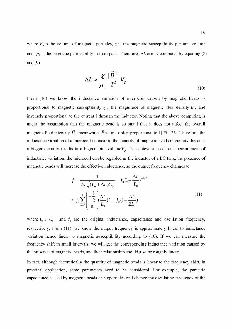
where pV is the volume of magnetic particles, χ is the magnetic susceptibility per unit volume
and 0μ is the magnetic permeability in free space. Therefore, LΔ can be computed by equating (8)
and (9)
2
20
| |p
BL VI
χμ
Δ ≈ (10)
From (10) we know the inductance variation of microcoil caused by magnetic beads is
proportional to magnetic susceptibility χ , the magnitude of magnetic flux density B , and
inversely proportional to the current I through the inductor. Noting that the above computing is
under the assumption that the magnetic bead is so small that it does not affect the overall
magnetic field intensity H , meanwhile B is first-order proportional to I [25] [26]. Therefore, the
inductance variation of a microcoil is linear to the quantity of magnetic beads in vicinity, because
a bigger quantity results in a bigger total volume pV . To achieve an accurate measurement of
inductance variation, the microcoil can be regarded as the inductor of a LC tank, the presence of
magnetic beads will increase the effective inductance, so the output frequency changes to
1/ 20
00 0
1
0 00 0 0
1 (1 )2 ( )
1( ) (1 )2
20
n
n
Lf fLL L C
L Lf fL L
π−
=
Δ= = +
+ Δ
⎛ ⎞− Δ Δ⎜ ⎟≈ = −⎜ ⎟⎝ ⎠
∑ (11)
where 0L , 0C and 0f are the original inductance, capacitance and oscillation frequency,
respectively. From (11), we know the output frequency is approximately linear to inductance
variation hence linear to magnetic susceptibility according to (10). If we can measure the
frequency shift in small intervals, we will get the corresponding inductance variation caused by
the presence of magnetic beads, and their relationship should also be roughly linear.
In fact, although theoretically the quantity of magnetic beads is linear to the frequency shift, in
practical application, some parameters need to be considered. For example, the parasitic
capacitance caused by magnetic beads or bioparticles will change the oscillating frequency of the

17
LC tank, thus making the final frequency output nonlinear to the quantity of magnetic beads.
Moreover, a good microcoil sensor needs to differentiate less magnetic beads located at stronger
magnetic field region and more magnetic beads located at weaker magnetic field region, due to
the non-uniformity of the magnetic field generated by microcoil. Therefore, the design of a
microcoil sensor is critical. The above mentioned issues will be addressed in Chapter 4 by
proposing the design of a microcoil sensor.

18
CHAPTER 2 STATE OF THE ART OF THE LAB-ON-CHIP
MICROSYSTEMS USING MAGNETIC BEADS
Lab-on-chip is a multidisciplinary approach used for the miniaturization, integration and
automation of biological assays or procedures in analytical chemistry [27]. To realize a complete
LoC microsystem, various technologies are required, such as microfluidics, microelectronic
circuits, sensor technologies and packaging techniques. The microscopic handling of biological
particles has gained great progress, with the development of microfluidics and microfabrication.
We review in this chapter the state of the art of these technologies for bioparticles manipulation
and detection using magnetic beads.
2.1 Labeled and Non-labeled Manipulation and Detection of Bioparticles---A Comparison
A variety of techniques have been reported for bioparticles manipulation and detection, and they
can be classified to different types according to various classification methods, for example,
according to whether bioparticles are labeled or not.
Non-labeled manipulation applies direct handling on bioparticles, exempting from the preparation
of labels attach and detach. For example, mechanical micro tweezers[28] can pick and place the
bioparticles in microscale for micro-surgery and tissue engineering, the manipulation is accurate
and fast, but the mechanical fatigue of material limits its use. Optical manipulation, sometimes
called optical tweezers, takes advantage of the forces generated by a strongly focused beam of
light to trap and move objects ranging in size from tens of nanometres to tens of micrometres[29].
It can achieve high throughput manipulation but at the cost of high power consumption.
Additionally, it’s very hard to integrate all the optical components, such as laser, lenses and
motor, in a microsystem, which conflicts with our miniaturization target. Dielectrophoresis (DEP)
can be employed to electrically manipulate the polarisable particles induced by electric field
gradients[30][31], and an accurate manipulation can be achieved by applying high resolution
electrodes, however, there exists some disadvantage of dielectrophoresis. Since the DEP force is
proportional to the volume of the particles, which means when the size of particle decreases,
higher electric field intensity is needed for generating the force to resist Brownian motion. Higher
electric field intensity is from high voltage signal between electrodes, which may cause severe
ionic current flow and double layer polarization effects to damage bioparticles [32][33].

19
Therefore, it is generally impractical to use it for objects with characteristic lengths in nanometer
scale, such as DNA and some antibody-antigens [25].
Non-labeled detection of bioparticles relies on the contrast of some parameters between
bioparticles and background liquid. For example, resistive biosensor measures the resistance
difference between bioparticles and medium[34][35] whereas capacitive biosensor measures the
capacitance difference[36][37], these biosensors are easy to be implemented, as the techniques
regarding resistance and capacitance measurement are mature, however, the subtle difference
between bioparticles and background liquid environment results in extremely high requirement
for the sensitivity of such biosensor, which is not easy to be realized. Usually, resistive and
capacitive biosensors are used in low sensitivity or large amount bioparticles detection; in order
to achieve higher sensitivity bioparticles detection, optical method is employed. For example,
single-photon avalanche diode (SPAD) detects the presence of bioparticles by counting the
photons blocked by bioparticles[38][39], the sensitivity can be qualified for single bioparticle
detection, depending on the design of SPAD. The disadvantage of this method is that an external
light source needs to be installed, which is difficult to be miniaturized and integrated. A common
drawback for all the above mentioned non-labeled detection techniques is that these biosensors
are non-specific. Regarding the complexity of biological environment, multiple types of
bioparticles usually coexist, whereas their resistances, capacitances or sizes are comparable in a
short range, so it’s very difficult to differentiate them.
On the other hand, labeled bioparticles are manipulated indirectly by manipulating the labels. For
example, magnetic beads as labels or carriers of bioparticles can be manipulated by magnetic
field generated by permanent magnets or electromagnets. Due to the high magnetic susceptibility
of magnetic beads, a very accurate and sensitive manipulation can be achieved. The labeled
bioparticles detection relies on the detection of bio-labels to reflect the existence of
corresponding bioparticles. For example, fluorescent labeling is a process of covalently attaching
fluorophores to target bioparticles, such as protein or nucleic acid. Fluorescence-labeled
bioparticles can then be detected by measuring the intensity of scattered light[40] [41] via a
fluorescence microscope, flow cytometer or some other fluorescence reading instrument. It’s a
widely used method in localization of a target within a cell[42], however, it also suffers from
several disadvantages such as photo-bleaching, spectral overlap and additional bulky detection
equipment [43][44][45][46]. These constraints have inspired the efforts of researchers to develop

20
the detection method using other bio-labels, for example, magnetic bead. Magnetic micro/nano
particles and magnetic sensor based bioassay is called magnetic immunoassay (MIA)
[47][48][49][50]. The detection of magnetic beads labeled bioparticles relies on the measurement
of the magnetic susceptibility of medium in vicinity of magnetic sensor[26]. Magnetic beads as
bio-labels offer a number of advantages over fluorophores labels, for example, there is no
significant magnetic background present in biological environment, thus the noise interference
can be minimized; magnetic beads are biocompatible and stable over time; magnetic beads as
labels of bioparticles can also be manipulated by magnetic field during detection, thus various
applications are possibly be achieved by configuring the local magnetic field.
2.2 Microsystems for Magnetic Beads Manipulation
Since the magnetic beads are used as carriers of various bioparticles, the mechanisms applied in
the manipulation of bioparticles are actually same as the manipulation of magnetic beads.
Different types of magnetic beads manipulation on microsystems, such as trapping, sorting,
transporting, have been presented[51][52][53], and the most commonly used magnetic beads in
those applications are ranging from 1µm to 10µm. As for the magnetic field, it can be generated
by either permanent magnets or electromagnets.
Figure 2.1 Magnetic bead separator employing permanent magnets[54].

21
A microfluidic magnetic bead separator for high-throughput applications is introduced in [54].
This microsystem consists of an array of small Nd–Fe–B permanent magnets and an array of
integrated permalloy elements which are encapsulated in the bottom of a separation chamber. The
permanent magnets can provide magnetic forces with a resolution of millimeter, whereas the
integrated permalloy elements are employed to enhance the local forces on 10µm scale near the
bottom of separation chamber. Due to the use of permanent magnets, a strong magnetic field can
be generated, thus the a high efficiency of magnetic beads separation (~90%) was achieved.
However, the disadvantage of using permanent magnets in microsystem is that the magnetic field
distribution is fixed once the microsystem is fabricated, thus reconfigurable and flexible control
of magnetic field are difficult. Meanwhile, the fabrication process to integrate permanent magnets
is usually non-standard and not compatible with modern microelectronic fabrication technology.
Therefore, in smart medical and biological device, planar electromagnets, which can be massive
produced and integrated with microfluidic structures, are more preferred to be used as magnetic
field generator.
Figure 2.2 A microsystem combining permanent magnets and electromagnets. Cu current lines
are buried in the back side of the substrate at the positions indicated by the white lines.
Another hybrid magnetic bead separator demonstrated in [55] combines an external magnetic
field with current lines as thick as 175 mm buried in the back side of a silicon wafer so that the
magnetic beads can be activated by the uniform external strong magnetic field as well as
manipulated by the on chip electromagnets. The use of electromagnets adds flexibility to this

22
microsystem, but the current through Cu metal is as high as 2A, which results in very high power
consumption. Another drawback of applying big current lines is that due to the Joule heat
generate by high current, a cooling system has to be added to avoid the overheat spots, thus the
total power consumption and system complexity are further increased. These disadvantages
inspire the researchers to explore how to reduce the current to generate the required magnetic
field to manipulate magnetic beads. The most effective and economic way is to improve the
design of electromagnets, including the geometry and topology. Fortunately, with the
development of finite element analysis (FEA) software, the magnetic field generated by
electromagnets can be simulated and optimized before implementing, thus more and more
designs of the micro electromagnets aiming for higher manipulation efficiency have been
proposed.
Figure 2.3 A summary of the performance of various planar electromagnets. Row 1: a schematic
view of the microcoil; row 2: image under optical microscope; row 3: the simulated magnetic
flux density profile; row 4: schematic of the magnetic bead trapping profile and; row 5: optical
image of the magnetic beads trapped by corresponding microcoils [56]
Various designs of planar micro electromagnets and their FEA simulation results have been
presented in [57][58][59][60][56][61]. The comparison of different geometrical configurations in
Fig. 2.3 has concluded that planar spiral microcoil results in the best power efficiency, i.e. in a

23
given area, spiral microcoil will generate the biggest total magnetic flux density and steepest
magnetic field gradient. Adding ferromagnetic pillar to the center of microcoil will further
enhance the local magnetic field, but at the cost of extra fabrication steps and cost. Fig. 2.4 shows
the implementation of a magnetic pillar on a silicon substrate microsystem. It’s worth noting that
although spiral microcoil generates the strongest magnetic field, it is not always the best option,
because in order to make a spiral microcoil, at least two metal layers are required, which is not
always available for many fabrication processes. Moreover, the magnetic field distribution of a
spiral magnetic field is not as uniform as other geometries, for example, serpentine, so it’s not
necessarily always the best option in some magnetic beads applications. One has to consider
multiple facts when designing the planar electromagnets for LoC applications.
Figure 2.4 (a) Schematic of the microsystem with the fluidic chamber on top of the coil and pillar;
(b) Prototype of final fluidic device with chip inserted in. The size of the fluidic chamber is
10mm×5mm×0.1mm. The fluidic inlet and outlet, with inner diameter of 0.5 mm. The fluidic
block is connected to a programmable syringe pump fitted with a 1 ml syringe[61].
In addition to generating magnetic field within a coil’s layout region, a planar microcoil is also
possible to cooperate with adjacent microcoils to form a combined magnetic field. While
extending the control region from single coil to coil array, more diverse functions can be
achieved. Two silicon substrate based microsystems which integrate microelectronic circuits and
microcoil array are introduced in [62] and [63], which aim for magnetic beads cluster
manipulation and individual magnetic beads manipulation, respectively. By controlling the on
and off of specific microcoil in the array, and applying corresponding control algorithm, different
applications, such as trapping and transporting, can be realized. For example, in Fig. 2.5, the

24
transport of magnetic beads cluster is realized by an algorithm that current pulses with
appropriate values and directions are alternatively applied to two neighboring microcoils. Thanks
to the development of Very-Large-Scale Integration (VLSI) circuits, controlling a large scale
microcoil array at a high efficiency is not a difficult task any more. All parameters regarding
microcoil array controlling, such as current intensity and current direction can all be flexibly
customized.
Figure 2.5 Microcoil array for magnetic beads manipulation. By controlling currents in the
microcoils, many different magnetic field patterns can be generated. To generate the required
fields, current pulses with appropriate values and directions are alternatively applied to two
neighboring microcoils[62].
Another microsystem shown in Fig. 2.6 employs similar microcoil array and control algorithm as
in [62], but for the purpose of individual magnetic beads manipulation. Individual magnetic
beads manipulation follows the same mechanism as beads cluster manipulation, but usually
requires higher control resolution. The manipulation resolution is highly relative to the size of
microcoil and limited by fabrication process. The perfect case would be that the size of a
microcoil is the same as that of a magnetic bead, thus an extremely accurate control can be
achieved. Another point that is worth mentioning is that the microsystem in Fig. 2.6 exploits open
cavity as microfluidic packaging, therefore it is a fast prototyping method, though not very
reliable for practical use.

25
Figure 2.6 An open cavity microsystem integrating CMOS coil array for individual magnetic
bead manipulation [51].
Although it has been demonstrated that planar microcoil based microsystem is capable of
manipulate magnetic beads for different applications, such as trapping, sorting and transporting,
it’s worthy of further research on the design of microcoil array, because previous research only
exploited simple geometrical microcoil and controlling scheme, whereas a universal optimization
method for the design of microcoil array to achieve the highest efficiency is lacked. Moreover,
the inevitable overheat spot issue for electromagnets in microfluidic applications, is often ignored,
thus a safe temperature range for vital bioparticles is hard to be maintained. Additionally,
previous microsystems are either open cavity, for which the liquid is directly exposed to the air,
or using customized processes to achieve microfluidic structures, whereas a robust
microfluidic/microelectronic interface taking advantage of standard packaging technology is
rarely reported. Therefore, the above presented microsystems are mostly confined in laboratory.
These constraints are addressed in Chapter 3 and Chapter 5 of this thesis work and resolved by
our proposed microsystems.

26
2.3 Microsystems for Magnetic Beads Detection
Accurate and effective detection of bioparticles in microfluidic is always a challenging work, as
several criteria need to be respected simultaneously, including repeatability, accuracy, stability,
cost and most importantly, the viability of bioparticles. In magnetic beads applications, the
detection of bioparticles is represented by the detection of magnetic beads, because the
bioparticles are attached to the magnetic beads. The main advantage is that a high signal to noise
(SNR) ratio can be achieved, since magnetic beads as labels of bioparticles show strong contrast
to non-magnetic background biological environment. To detect the bioparticles attached magnetic
beads, various biosensors have been reported, including Hall sensor, Giant Magnetoresistance
(GMR) sensor, Nuclear Magnetic Resonance(NMR) sensor, and inductance sensor[64][43]. In
this chapter, we summarize all these techniques with emphasis on inductance measurement based
sensor, as this sensor uses the low cost coil as inductor and the fabrication process is compatible
with regular integrated circuits thus it provides significant cost advantage over others.
Additionally, planar microcoil based inductance sensor can take advantage of the manipulation
capability of the same coil, thus a multifunctional LoC microsystem can be achieved on the same
substrate.
2.3.1 GMR Sensor
GMR is a quantum mechanical magnetoresistance effect observed in thin film structures
composed of alternating ferromagnetic and non magnetic layers[65]. The 2007 Nobel Prize in
physics was awarded to Albert Fert and Peter Grünberg for the discovery of GMR. Depending on
whether the magnetizations of adjacent ferromagnetic layers are in parallel or anti-parallel
alignment, a significant change in the electrical resistance can be observed. The total resistance is
relatively low for parallel alignment of adjacent layers and relatively high for anti-parallel
alignment.
Recently, GMR has been drawing attention for the application in biochip. For example, Figure
2.7 shows a proposed integrated silicon substrate based GMR sensor for magnetic particles
detection [54]. It includes four spin-valve GMRs wired as Wheatstone bridges. In each bridge,
two GMRs act as sensing resistors and are located under a microfluidic channel. The other two
GMRs serve as reference resistors, which are located beneath the insulation layer and separated
from the edge of the neighboring sensing GMRs. As the magnetic particles approach the sensing

27
GMRs, the magnetic field increases, which in turn gives rise to an increase in the sensing GMR
resistances and therefore a decrease in the voltage drop (E2-E1) across the bridge. As the front of
the magnetic particles moves past the sensing GMRs, the magnetic field will decrease rapidly and
the response then slowly decreases as the middle of the magnetic particles flows across the
sensing GMRs.
Figure 2.7 Schematic of a GMR based magnetic flow sensor design [54]
This design demonstrates the sensing of individual ferromagnetic particle in flow, and indicates
that for the sake of detecting magnetotactic bacteria or superparamagnetic beads, one may require
to redesign the sensors by shrinking its size. Employing GMRs as biosensors promises a number
of advantages. First of all, the GMR sensors are compatible with the established CMOS processes
and are able to provide an electronic signal directly suitable for automated analysis. They are
scalable and can be tailored in geometry to meet any desired functionality. Furthermore, there is
no background signal if unspecifically bound magnetic markers are avoided, thus the signal to
noise ration can be high. Contrary to fluorescent markers, magnetic beads as markers are over
time stable, so that measurements can be repeated many times. Additionally, the miniature size of
GMR sensor allows for the combination of magnetic beads detection with manipulation, because
the magnetic beads carrying the analytical molecules can be manipulated on chip to specific

28
binding sites where GMR sensors locate. Such flexibility make GMR biosensors a good
candidate for hand-held lab-on-a-chip devices [66].
However, the utilization of GMRs in Lab-on-chip brings enormous increases in cost, because
GMR fabrication on silicon is not a standard CMOS process and some special materials are used
to achieve a good performance. In the given example above, a deposition process of Ta, NiFeCo,
CoFe, Cu and CrPtMn is required. For this reason, the research about GMR applied in biochip
has been staying in laboratory for a long time.
2.3.2 Hall Sensor
Hall Effect has been well studied and widely used in many applications. The principle behind
Hall Effect is that when an external magnetic field is applied, the charge carriers in a conductor
experience magnetic force and are moved away from the nominal current direction. This
phenomenon leads to a transverse electrical field, which eventually stops the carrier drift and can
be measured as a transverse electrical potential which is called Hall voltage[67].
Recently, the Hall Effect has been attracting the attentions in the field of biosensors, because it
can be utilized to implement magnetic biosensors for magnetic particles detection[68][69]. For a
typical Hall sensor as shown in Fig. 2.8, the magnetic bead is firstly immobilized on the sensor
surface through specific method, either by magnetic field or physical placement. Then, an
external magnetic field is applied to polarize the magnetic bead which produces a stray magnetic
field. The combination of the excitation field and the stray field is then measured by reading out
the output voltage the Hall sensor, thus the presence of magnetic bead can be detected. Hall
sensors are fully compatible with standard CMOS processes without any requirement for
expensive metal, compared with GMR sensor, because they can be realized using retrograded n-
well or active region of a MOS transistor[68]. It is worth mentioning that the distance between
the magnetic bead and the sensor surface must be minimized to receive the biggest signal due to
the stray field. Therefore, a metal wet etching has to be conducted on the silicon chip to remove
the passivation layer on top of the Hall sensor. This is considered as a drawback of Hall sensor
because additional post processing steps result in additional cost and lower yield. Note that the
external biasing magnetic field shown in Fig. 2.8 can also be generated on-chip, for example
using metal wires. In this way, the system setup and cost can all be reduced.

29
Figure 2.8 A conceptual schematic view of a Hall sensor for single magnetic particle
detection[69]. An external magnetic field is applied to polarize the magnetic bead which
produces a stray magnetic field.
The active area of the Hall sensor in Fig. 2.8 is 2.4µm by 2.4µm which is a similar to the size of a
single magnetic bead. In order to detect large quantities of magnetic beads, usually Hall sensors
array can be implemented. For example, in one reported design, the sensor chip is realized in a
0.18 µm CMOS process, it contains 64 sensor units and is capable of detecting one single 4.5 µm
magnetic particle for each sensor[68]. Another design in a 0.25 µm CMOS process achieves
1,024 sensing units and immunoassay experiments were conducted[70]. The immunoassay results
based on this sensor implementation demonstrated the protein detection limit of 1 nano gram per
micro liter, which is a comparable sensitivity with traditional biomedical method.

30
The main disadvantage of Hall effect sensor is that a strong and uniform magnetic field is
required to polarize magnetic beads before detection, normally, this magnetic field can only be
generated by external ferromagnets, which adds cost and volume to the overall device, or very
large current on-chip electromagnet, which is very power consuming. Additionally, a post
fabrication process for silicon chip is required to the passivation layer on top of Hall sensor,
which further increases the fabrication complexity and cost.
2.3.3 NMR Sensor
Nuclear magnetic resonance (NMR) is a physical phenomenon in which nuclei in a magnetic
field absorb and re-emit electromagnetic radiation[71]. NMR relaxometer as magnetic sensor
explores the change in the bulk spin-spin relaxation time of water molecules to indirectly reflect
the presence of magnetic bead [72]. It is very different from GMR sensor and Hall sensor, both of
which utilize the stray field of polarized magnetic beads for detections. A typical implementation
for NMR sensor is shown in Fig. 2.9. A proximity assay is needed to be employed in such sensor,
which assumes that functional magnetic beads are first in monodisperse state in the medium.
Once the under-test analyte is introduced, it triggers the binding and aggregation of the magnetic
beads. This leads to self-assembled magnetic clusters in the medium, de-phases the nuclear spin
of the surrounding water molecules, and decreases the bulk spin-spin relaxation time. By
measuring the relaxation time T2, the quantity of magnetic beads can be reflected. Because of the
self-amplifying nature of the proximity assay, this sensing scheme has the potential to achieve a
very high sensitivity.
The complete NMR relaxation measurement setup requires key components including a large
external magnetic field, usually in Tesla range, a transmitting/receiving coil, and
transmitter/receiver circuits to generate the excitation magnetic field and receive the NMR
relaxation signal. Either high-power electromagnet or rare-earth magnet is required to realize
such strong biasing magnetic field, while the biasing field in Hall sensors can be generated on-
chip. This requirement on an external magnet significantly increases the overall system
complexity and cost. Moreover, in practical applications, due to this strong magnetic field,
appropriate shielding techniques are needed to safeguard both the sensor and the nearby
environment. An implementation reported in [72] utilizes integrated transmitter and receiver
circuits in a 0.18 µm CMOS process; the transmitting/receiving coil remains off-chip due to its

31
large size required by the low-frequency operation. A refined version of the NMR relaxometer
successfully integrates the transmitting/receiving coil on-chip, offering a compact NMR
relaxometer sensor solution and also reducing the size of the rare-earth magnet. Microfluidic
network is implemented and integrated to enable sample feeding and proximity assay reactions.
The NMR relaxometer sensor is characterized based on detecting actual bio-samples. The sensor
achieves avidin detection at 3 nano mole concentration. Bacteria detection using Staphylococcus
aureus is also tested, and the sensor is capable of registering as few as ten bacteria in a 10 nL
sample. Mammalian cell detections are also performed, which shows a detection limit of 17.5
cells per nano liter for human bladder cancer cells and one single magnetically modified
macrophage cells per 10nL medium.
Figure 2.9 Conceptual drawing of the NMR relaxometer and its proximity assay [59]. (a) The
bulk spin-spin relaxation time T2 for water molecules without test samples. (b) The relaxation
time is reduced with monodispersed magnetic particles. (c) The target molecule i.e., proteins,
trigger the proximity assay and lead to aggregation of magnetic particles to form clusters, which
further decrease the relaxation time of the water molecules.
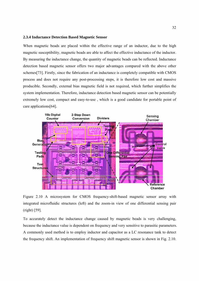
32
2.3.4 Inductance Detection Based Magnetic Sensor
When magnetic beads are placed within the effective range of an inductor, due to the high
magnetic susceptibility, magnetic beads are able to affect the effective inductance of the inductor.
By measuring the inductance change, the quantity of magnetic beads can be reflected. Inductance
detection based magnetic sensor offers two major advantages compared with the above other
schemes[73]. Firstly, since the fabrication of an inductance is completely compatible with CMOS
process and does not require any post-processing steps, it is therefore low cost and massive
producible. Secondly, external bias magnetic field is not required, which further simplifies the
system implementation. Therefore, inductance detection based magnetic sensor can be potentially
extremely low cost, compact and easy-to-use , which is a good candidate for portable point of
care applications[64].
Figure 2.10 A microsystem for CMOS frequency-shift-based magnetic sensor array with
integrated microfluidic structures (left) and the zoom-in view of one differential sensing pair
(right) [59].
To accurately detect the inductance change caused by magnetic beads is very challenging,
because the inductance value is dependent on frequency and very sensitive to parasitic parameters.
A commonly used method is to employ inductor and capacitor as a LC resonance tank to detect
the frequency shift. An implementation of frequency shift magnetic sensor is shown in Fig. 2.10.

33
The current through the inductor of a LC tank generates a local magnetic field which will
polarize the nearby magnetic beads. Due to the high magnetic susceptibility of magnetic beads,
the total magnetic energy is increased as well as the effective inductance of the resonator, which
subsequently leads to a down-shift of resonant frequency of the LC tank. Then the resonant
frequency can be read out to indicate the quantity of magnetic beads.
Figure 2.11 Inductance detection based magnetic sensor for detecting DNA [64]
The main concern of designing the above mention magnetic sensor is the sensitivity, because the
frequency shift could be too small be accurately extracted from the circuit noise, especially when
aiming to detect low density magnetic beads. Usually, a combination of careful design of front
end inductor sensor with low phase noise on-chip oscillator is preferred. For example, a ultra-
high-frequency shift magnetic sensor which combines on-chip circuit and LC oscillators has been
achieved in [64] , this microsystem can be used for DNA detection and single magnetic bead
sensitivity is claimed. The concept is shown in Fig. 2.11. It takes advantage of the concept of
magnetic immunoassay. Magnetic bead is used as the label of anti-digoxigenin, which forms a
sandwich structure with DNA and biotin molecule, so the presence of specific DNA can be
reflected by the measurement of magnetic bead. To note that although the principle of frequency
shift magnetic sensor is not difficult to be understood for qualitative detection, the practical
employment for quantitative detection is not easy, because a lot more parameters need to be
considered, including interference of parasitic capacitance, nonlinearity, noise from circuits and
temperature shift issue. To achieve a high sensitivity and good linearity sensor for quantitative

34
detection, one has to optimize the design of microcoil associated with the sensing signal
conditioning circuit by dedicated design optimization and high circuit complexity.
Above all, to achieve the widespread adoption of magnetic sensors for medical diagnosis and
environment monitoring applications, there are still several technical challenges that need to be
addressed, the pros and cons of each aforementioned magnetic sensing schemes need to be
considered to decide the most appropriate scheme for specific application. Moreover, many
aforementioned magnetic sensors show high sensitivity, or even single magnetic bead sensitivity,
however, in practical applications, in addition to high sensitivity, good linearity is also an
important feature for quantitative measurement. A reliable measurement needs both accuracy and
repeatability. Moreover, magnetic sensors, like many high precision sensors, may present
environment related long term signal drift, for example in the frequency-shift magnetic sensors.
Although differential sensing and advanced noise cancellations scheme can largely suppress such
drifts, new refinement techniques for drift removal are highly desirable. We address the above
issues in Chapter 4 by proposing the design of a microcoil magnetic sensor with good linearity,
and a scheme to ease the signal drift due to temperature varying.
2.4 Microsystems Packaging Techniques
A robust microfluidic/microelectronic package can facilitate the prototyping of microsystem and
bolster reliable experimental operation. However, packaging for microfluidic chip has historically
been a challenging work, because microfluidic devices typically require multiple interconnects
and in many cases the packaging components are much larger than the microelectronics
interfaces. Usually, these microfluidic packaging structures, including but not limited to
microchannels, chambers, and wells should be performed using a low temperature process with
reliable bonding, since the leakage of reagents from microfluidic components may bring
contamination and increase the parasitic capacitance or resistance of microelectronic circuits.
Various packaging techniques have been applied to realize microelectrnic/microfluidic hybrid
microsystem.
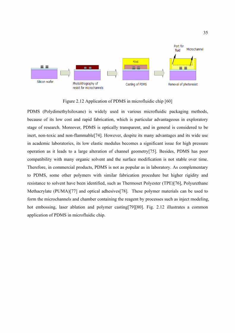
35
Figure 2.12 Application of PDMS in microfluidic chip [60]
PDMS (Polydimethylsiloxane) is widely used in various microfluidic packaging methods,
because of its low cost and rapid fabrication, which is particular advantageous in exploratory
stage of research. Moreover, PDMS is optically transparent, and in general is considered to be
inert, non-toxic and non-flammable[74]. However, despite its many advantages and its wide use
in academic laboratories, its low elastic modulus becomes a significant issue for high pressure
operation as it leads to a large alteration of channel geometry[75]. Besides, PDMS has poor
compatibility with many organic solvent and the surface modification is not stable over time.
Therefore, in commercial products, PDMS is not as popular as in laboratory. As complementary
to PDMS, some other polymers with similar fabrication procedure but higher rigidity and
resistance to solvent have been identified, such as Thermoset Polyester (TPE)[76], Polyurethane
Methacrylate (PUMA)[77] and optical adhesives[78]. These polymer materials can be used to
form the microchannels and chamber containing the reagent by processes such as inject modeling,
hot embossing, laser ablation and polymer casting[79][80]. Fig. 2.12 illustrates a common
application of PDMS in microfluidic chip.

36
Figure 2.13 Fabrication procedure of DWFP technique: (a) ink deposition, (b) encapsulation in
epoxy and (c) ink extraction [81].
In addition to these conventional packaging techniques, recently, direct-write fabrication process
(DWFP) has also been proved to be a promising technique for microfluidic/microelectronic
hybrid system fast prototyping. It is a fugitive ink based, robot assisted fast microchannel
prototyping method. Normally, it only takes a few hours to finish the whole prototyping. Layer-
by-layer structures composed of filaments with cylindrical, hexagonal or square cross sections
can be produced. The filaments are formed during the extrusion of a paste-like material through a
micro nozzle and deposited on a substrate in order to build planar or three-dimensional (3D)
structures[82]. The deposition of a fugitive organic ink scaffold was then conducted by the
infiltration of an uncured epoxy resin. After polymerization, the ink is extracted at moderate
temperature in order to obtain the desired microfluidic network[81]. DWFP is compatible with
standard CMOS technology as well as any other planar layer-by-layer structures based
technologies, such as PCB and glass. Compared with conventional polymer processes, DWFP is
a more automatic and standard technique with higher resolution. Part of this thesis work benefits
from DWFP technique on prototyping and packaging of microfluidic chip.

37
Figure 2.14 A Sensonit glass substrate based hybrid microsystem [69].
An alternative material to polymer for microfluidic chip packaging is glass. Even though glass
micromachining needs more time and higher cost compared to polymer, it is still a favorable
choice to build microfluidic chip, due to its superior optical properties, surface stability, solvent
compatibility and excellent resistance to high pressure. Nowadays, glass substrate based
microfluidic chip can be fabricated through commercial available processes. For instance,
Sensonit is a microfluidic prototyping technology offered by Micronit Microfluidics BV. This
technology enables users to realize microfluidic structures and integrated metal electrodes in the
same glass substrates for microfluidic applications. Moreover, it allows for the integration of
CMOS sensor to achieve a hybrid microsystem. Sensonit can be used in various physical and
chemical applications, as well as applications in the life sciences, e.g., cell manipulation, genetic
analysis, medical diagnostics, protein and peptide analysis, microchemical analysis, drug delivery,
and DNA analysis. However, this technology is not always suitable for planar microcoil
fabrication, because complicated spiral topology is hard to be realized as no through layer vias

38
are provided between different metal layers. Therefore, for magnetic field generation, only those
electromagnets with simple geometries can be exploited.
In conclusion, microfluidic/microelectronic hybrid microsystem packaging requires various
technical steps, such as substrate micromachining, bonding, and sealing, whereas different
techniques can be employed according to the requirement of project in terms of cost, time,
complexity, etc. Fast prototyping techniques are usually low cost but labor intensive, so they are
usually exploited at laboratory stage to verify the concept. On the other hand, standard techniques
are more expensive and take more time but with better robustness, they are usually the preference
for industrial products.

39
CHAPTER 3 A TEMPERATURE CONTROLLABLE PLATFORM FOR
MAGNETIC BEADS MANIPULATION
3.1 Introduction
A fully functional LoC using magnetic beads for bioassay has great potential in automated health
and environmental applications. As the labels of bioparticles, magnetic beads need to be
manipulated according to specific requirement, such as trapping, separating, sorting and
transporting. Since the behavior of magnetic beads is affected by the magnetic field in vicinity, a
flexible and accurate control of magnetic field on chip is required. Two-dimensional planar
microcoil array is a good candidate for generating a controllable magnetic field, because it can be
flexibly configured by microelectronic controlling circuits and is scalable. However, the magnetic
field generated by planar microcoil is usually weak, unless a big current is applied. Due to the big
current and non-symmetrical layout, Joule heat is significant and results in overheat spot. This
issue was widely mentioned but usually treated by an additional complicated cooling system,
which highly increases the system complexity and total power consumption. In fact, it is possible
to model the heat generating process for the microcoil array by FEA software, and exploit
advanced control method to reduce the Joule heat, without increasing the complexity of hardware
system design. In parallel, the microcoil array’s geometry layout can be improved to achieve
more uniform “heating spots” to avoid the “overheating spot” in conventional LoC device, so that
the temperature of liquid can be maintained within the safe range to bioparticles.
In this chapter, the design and implementation of a compact LoC platform dedicated for magnetic
beads based bioparticles manipulation is introduced. For this platform, it takes advantage of a
planar microcoil array to generate distributed magnetic field, and by the incorporation of multiple
microcoils, magnetic beads can be manipulated in different ways, leading to different
applications such as trapping, separation and mixing. Moreover, instead of using an external
cooling system, an advanced current supply method is applied to reduce the Joule heat and
maintain the controllable temperature in liquid. The microcoil array is fabricated in a very thin
polyimide substrate based on a standard and mass-producible double metal layer process. The
concepts were verified by both simulations in FEA software and experiments using artificial
magnetic beads. The following section is the reproduction of an article published in IEEE
Transactions on Magnetics, Vol.49, No.10, pp.5236-5242, Oct. 2013.

40
3.2 Planar Microcoil Array Based Temperature-controllable Lab-on-Chip Platform
3.2.1 Abstract
In this paper, we present the design and implementation of a planar microcoil array based
temperature-controllable Lab-on-chip (LoC) platform for magnetic bead manipulation. Magnetic
beads are used as the solid phase carriers of bioparticles and microcoil array acts as the scattered
magnetic field source to manipulate the magnetic beads in microfluidics. Meanwhile, the Joule
heat issue, which is inevitable and often considered as drawback of electromagnetic LoC
applications, is analyzed and proved to be controllable using our proposed current supply method.
With this method, microcoil can be used as heat source to keep the temperature of microfluidic
within the safe range for bioparticles, saving the external incubator. To verify the concept, a
polyimide substrate LoC platform was fabricated and tested. Taking advantage of the
commercially available process, it is standard and mass-producible. Experimental results show
that both individual single bead and mass beads varying from 1µm to 2µm can be manipulated
with acceptable current consumption, while temperature can be maintained in a safe range.
Index Terms— Planar coil array, Lab-on-Chip (LoC), Joule heating, Magnetic beads, Polyimide
substrate
3.2.2 Introduction
Emerging Lab-on-Chip (LoC) devices have been perceived as a promising technology ever since
its concept was first introduced, due to the advantages such as low consumption for samples,
small size for device and short analysis time [83]. One of the most popular applications of LoCs
is bioparticles manipulation, for which several techniques are performed, such as
dielectrophoresis [31], magnetophoresis [84] and optical field [85]. Among them, the usage of
magnetic beads to manipulate bioparticles (e.g. cells, proteins, DNA) in microfluidics has been
attracting noticeable attention due to the high controllability and good biocompatibility,
compared with other techniques mentioned above. Magnetic beads are actually the solid phase
carriers of bioparticles as depicted in Fig. 3.1, they can be manipulated by applying magnetic
field in microfluidics, thus different applications can be realized by controlling the scattering of
magnetic field, such as separation, mixing, sorting, and transport [86] [87] [88]. For generating
the scattering magnetic field in microfluidics, in-channel or on-chip planar coils are preferable
compared with external ferromagnets, because magnetic flux intensity and direction can be

41
controlled simply by changing the current passing through the coils, thus resulting in a more
flexible control.
Figure 3.1 Magnetic beads as solid phase carriers for bioparticles manipulation
As for planar coil based bioparticles manipulation, some previous studies only involved
individual coils or simple topological coil array, whereas the coordination of multiple coils were
often neglected [56] [61] [89]. In those cases, the motion of bioparticles relies on the motion of
fluidic flow when bioparticles are out of the trapping range of individual microcoils, so an
external syringe pump is usually required to generate a moving fluid flow. Therefore, those
devices suffer from some drawbacks including low throughput, inaccurate manipulation, more
challenge for miniaturization and low-power efficiency. The most cost effective way for us to
overcome those drawbacks is to improve the topology of microcoil array to achieve a more
efficient manipulation, and to take into account the coordination of multiple microcoils to achieve
a bigger manipulating region, so that the migration of bioparticles between coils can be realized
without the help of external syringe pump, and with acceptable power consumption.
Another challenging issue in electromagnetic LoC applications is the inevitable Joule heating
effect. It was widely mentioned but usually treated by an additional complicated cooling system
[90] [55] [91], which highly increases the system complexity and power consumption. In fact, it
is possible for us to exploit some advanced control method to reduce the Joule heat, without
increasing the complexity of hardware system design. At the same time, we can improve the

42
microcoil array’s geometry layout to achieve more uniform “heating spots” to avoid the
“overheating spot” in conventional device, so that the temperature of liquid can be maintained
within the safe range to bioparticles.
In this paper, we describe the design and implementation of a compact LoC platform dedicated
for magnetic beads based bioparticles manipulation. For this platform, it takes advantage of a
planar microcoil array to generate distributed magnetic field, and by the incorporation of multiple
microcoils, magnetic beads can be manipulated in different ways, leading to different
applications such as trapping, separation and mixing. Moreover, instead of using an external
cooling system, we employ an advanced current supply method to reduce the Joule Heating effect
and maintain the controllable temperature in liquid. The microcoil array is fabricated in a very
thin polyimide substrate based on a standard and mass-producible double metal layer process.
The concepts were verified by both simulations in Finite Elements Analysis (FEA) software and
experiments using artificial magnetic beads.
3.2.3 Joule Heat Effect Analysis and Simulation
One inevitable but often neglected issue in microcoil array based LoC applications is Joule heat
effect. Coil heating strongly influences the maximum value of generated magnetic field [92], and
heating spot causes the formation of bubbles in liquid [93], moreover, it may heat up the
microfluidic solution, and then damage the viability of bioparticles, because most of the
bioparticles can only keep vital in a relatively narrow temperature range [94]. Therefore, the heat
generated by microcoils has to be controllable. Some previous studies used on-chip water cycling
system or external thermoelectric cooler to keep temperature in channel, which are proved
effective in holding temperature, but prior to these passive action, it is better to explore some
more economic means to control Joule heat by means of novel design concept or operation
principle. First, we investigate the heating process of a microcoil.
For a working microcoil, the induced Joule heat is
R=JQ JJ (1)
and the parabolic equation of temperature conduction is expressed [24] as
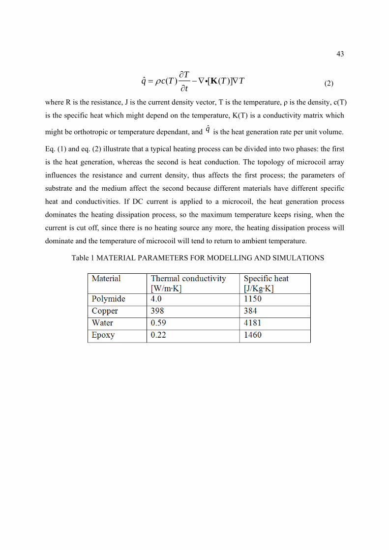
43
ˆ ( ) [ ( )]
Tq c T T T
tρ
∂= −∇ ∇
∂Ki (2)
where R is the resistance, J is the current density vector, T is the temperature, ρ is the density, c(T)
is the specific heat which might depend on the temperature, K(T) is a conductivity matrix which
might be orthotropic or temperature dependant, and q is the heat generation rate per unit volume.
Eq. (1) and eq. (2) illustrate that a typical heating process can be divided into two phases: the first
is the heat generation, whereas the second is heat conduction. The topology of microcoil array
influences the resistance and current density, thus affects the first process; the parameters of
substrate and the medium affect the second because different materials have different specific
heat and conductivities. If DC current is applied to a microcoil, the heat generation process
dominates the heating dissipation process, so the maximum temperature keeps rising, when the
current is cut off, since there is no heating source any more, the heating dissipation process will
dominate and the temperature of microcoil will tend to return to ambient temperature.
Table 1 MATERIAL PARAMETERS FOR MODELLING AND SIMULATIONS

44
JQ
Figure 3.2 The proposed closed-loop temperature control system.
Figure 3.3 3D Model of microcoil with channel and substrate in CoventorWare: (a) complete
model; (b) Substrate is hidden to show microcoil array.
Instead of applying a DC current to microcoil as in many previous works [61] [55], we propose
an AC current supply method with feedback from temperature sensor, to adjust the current signal
duty cycle, thus adjust the effective time of heat generation process and heat dissipation process
as depicted in Fig. 3.2. To verify this concept, we performed the Thermal Analysis in
CoventorWare for the model in Fig. 3.3, using the material parameters shown in Table 1. In this
model, copper, polyimide and epoxy were selected for the materials of microcoil, substrate and
microchamber, respectively. The fluid medium surrounding microcoil is deionized water. Copper
wire thickness is 35 µm; inner diameter is 500µm, outer diameter is 2mm. Note that specific heat
and conductivity are assumed to be constant to simplify the calculation, instead of temperature
dependent. The initial temperature for the model is assumed to be 300 K. Using the

45
mathematical formulas and simulation method introduced in our previous work [95], we first
obtained that a current intensity of 50mA could generate applicable magnetic field to manipulate
magnetic bead. Then we performed the thermal simulation with DC input. Starting from time 0, a
constant current with amplitude 50 mA was injected into the coil, causing the increase of
temperature on the contact surface of coil and liquid. After 5 seconds, the highest temperature
increment reached 3.4 K, and if it continued to increase, it could be dangerous to bioparticles. In
this case, the heat generation process dominates the heat dissipation process, so the maximum
temperature keeps rising. Then, a square wave current with amplitude of 50 mA and constant
frequency of 1 Hz was injected into the coil, over 5 seconds, we got the temperature varying
image in Fig. 3.4. Different from constant current, the maximum temperature image here was
flashing instead of continuously increasing.
Figure 3.4 Thermal propagation analysis when the input of a microcoil is constant-frequency
square-wave current.

46
Figure 3.5 Maximum temperature variation for different current inputs: (a) DC input; (b)
Constant frequency input---duty cycle 1:2 and frequency 1Hz; (c) Variable frequency input ---
duty cycle 1:2 and frequency 1Hz from 0 to 2.75s; duty cycle 1:5 and frequency 1Hz from 0 to
2.75s; duty cycle 1:5 and frequency 1 Hz after 2.75s.
Simulation results in Fig. 3.5 show that the final temperature increment is only 1.1 K, which is
67.6% lower than the constant current coil driving method. At last, we performed another
simulation with variable frequency input current. The duty cycle was changed from 1:2 to 1:5 at
time 2.75s. It shows that the temperature can be maintained roughly constant. In practical
applications, the frequency and duty cycle ratio of the input pulse waveform can be adjusted
according to the feedback from temperature sensor, and more advanced control technique, e.g.
PID-control can be applied, so that a controllable heat generation and heat dissipation can be
maintained. Another advantage of this method is that it is possible to use microcoil as heat source
to keep the temperature of microfluidic within the safe range for bioparticles, saving the external
incubator which is widely used in most biomedical applications.
One may argue that the magnetic beads could escape from the coil during the negative half-cycle
of input square-wave current. In fact, for a single magnetic bead in microfluidic, in addition to the
magnetic force, it experiences hydrodynamic drag force, gravitational force and buoyancy force,
299.5
300
300.5
301
301.5
302
302.5
303
303.5
304
0 1 2 3 4 5 6
Max Tem
perature /K
Time /s
DC Constant Frequency AC Variable Frequency AC
Potentially Dangerous Region a
b
c

47
whereas the latter two forces can be neglected due to bead’s small size and the cancellation of
each other in some degree. From Stokes’ law [18], we know
6 ( )drag bead bead fluidF R v vπ= η −
(3)
where beadv , fluidv , beadR and η are the bead velocity, microfluidic velocity, bead radius and fluid’s
viscosity, respectively. Now we consider the case when beads are immobilized at the center of
microcoils. If we turn off the coil, magnetic bead will be forced to move along the flow’s
direction due to eq. (3), at an initial velocity 0 and initial acceleration
6 /bead fluid beada R v mπ= η
(4)
where beadm is the mass of magnetic bead. Since in most microfluidic applications, fluidv is very
small, normally tens of micrometers per second, the acceleration is also very small, which means
the beads will not escape from the coil center area even when magnetic force is removed for a
short while. For example, when the velocity of fluid is 10 µm/s, one immobile magnetic bead
needs more than 3s to move over a distance of 10 µm. If we reactivate the coils within the beads’
escape time, the beads will be attracted to the center of coils again, from the macroscopic view,
the magnetic beads never leave. Note that Brownian motion here is neglected, with the
assumption that escape time due to Brownian motion is bigger than 10s [62]. One obvious
advantage of such kind of operation is that we can use digital switches to control the on and off
of microcoils, since the high speed of digital switches can be easily achieved, all the coils can
share one current source, which is definitely beneficial to power consumption and especially for
heating issue.
3.2.4 Current Supply Circuit
To achieve such a system as introduced in previous section, we need a bidirectional and
amplitude-variable current supply circuit. Meanwhile, considering that the multifunctional LoC
platform requires reconfiguration for different applications, we designed a CMOS circuit to
control the microcoil array. As the crucial microelectronic part of the whole LoC system, it was
firstly fabricated in TSMC 0.18 µm process, taking advantage of the ultra thick (2um) top metal
layer for big current path, and then mounted on the backside of the same substrate of off-chip
microcoil array. The bidirectional current source is connected to an addressable low on-resistance
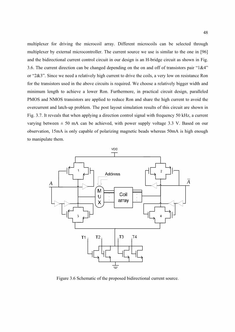
48
multiplexer for driving the microcoil array. Different microcoils can be selected through
multiplexer by external microcontroller. The current source we use is similar to the one in [96]
and the bidirectional current control circuit in our design is an H-bridge circuit as shown in Fig.
3.6. The current direction can be changed depending on the on and off of transistors pair “1&4”
or “2&3”. Since we need a relatively high current to drive the coils, a very low on resistance Ron
for the transistors used in the above circuits is required. We choose a relatively bigger width and
minimum length to achieve a lower Ron. Furthermore, in practical circuit design, paralleled
PMOS and NMOS transistors are applied to reduce Ron and share the high current to avoid the
overcurrent and latch-up problem. The post layout simulation results of this circuit are shown in
Fig. 3.7. It reveals that when applying a direction control signal with frequency 50 kHz, a current
varying between ± 50 mA can be achieved, with power supply voltage 3.3 V. Based on our
observation, 15mA is only capable of polarizing magnetic beads whereas 50mA is high enough
to manipulate them.
AA
Figure 3.6 Schematic of the proposed bidirectional current source.

49
Figure 3.7 Post layout simulation of bidirectional current supply circuit.
3.2.5 Device Architecture and Fabrication
For our proposed LoC platform, two main parts are included, namely reusable electronic device
and disposable microfluidic structure as shown in Fig. 3.8. The reusable device consists of the
microelectronic circuits for controlling the microcoil array and users interface for signal readout,
whereas the low cost microfluidic structure is for under-test liquid sample. The microfluidic
structure can be pulled off the microcoil array chip after test, and then a new microfluidic
structure can be remounted for the next test. The microcoil array is the connection between
microfluidics and microelectronics, since magnetic beads in microfluidic channels are activated,
manipulated and detected all by the microcoil array, whereas the behavior of microcoil array is
controlled by our proposed CMOS circuit. With the incorporation of microelectronic circuits, the
local magnetic fields can be reconfigured and programmed, thus various manipulations can be
achieved.

50
Figure 3.8 Architecture of the microcoil array based LoC platform.
Figure 3.9 The proposed polyimide substrate LoC device: (a) Hexagonal microcoil chip with
microfluidic structure; (b) Bottom view showing the heat dissipation layer and CMOS chip; (c)
Microphotograph of the CMOS chip; Die size 0.85mm by1.15mm; (d) Square microcoil array.

51
Although there are already a few LoC prototypes presented in previous works, most of them were
either simple microfluidic chip without electronics part or complicated microfluidic structures
combining microelectronics on silicon. In our study, we propose a novel LoC platform consisting
of low cost disposable microfluidic structure and reusable electronic part. The devices shown in
Fig. 3.9 are our proposed polyimide substrate LoC platform with different topological microcoils.
The substrate is a very thin all-polyimide composite of polyimide film bonded to copper foil. It’s
a low cost and mass producible product provided by Pyralux®. In this technology, the dielectric
thickness is only 100 µm, copper thickness is 35 µm. The minimum wire width and space
allowed by design rules are 50 µm and 75µm, respectively. Compared with the metal thickness
for silicon substrate which is usually below 3µm, the thicker metal in this process can tolerate a
higher current and leads to generate a stronger magnetic field. Meanwhile, the ultra thin dielectric
layer results in less magnetic energy loss and better heat dissipating, because we can add a
dummy metal layer in large area on the backside. To note that the dummy metal layer will cause
Eddy current which will cancel part of the magnetic field at high frequency, but this drawback
can be neglected at low frequency. Another significant advantage for this technology is that we
can make some pads on the back side of the substrate as shown in Fig. 3.9 (b). Therefore, the
integration of microfluidics and electronics will be easier and the miniaturization of device will
be possible. Indeed, it seems that the scheme of CMOS chip plus off-chip coil array has
limitation on the scale of microcoil array due to the countable I/O ports, but in most of the
practical biological applications, such as sorting, mixing, transporting, just several microcoils
would satisfy the requirement. Thus in these situations, it is not necessary to apply large scale of
microcoils. After all, if large scale off chip microcoil array is really needed, to say the least, we
just need to combine several CMOS chips to achieve the mass coils control.
The fabrication of microfluidic structures takes advantage of an efficient direct-write microfluidic
packaging procedure as introduced in the previous work of our research group [97] [98]. It is a
fugitive ink based, robot assisted fast microchannel prototyping method. Normally, it only takes a
few hours to finish the whole prototyping. Meanwhile, benefiting from the separation of
microelectronic part and microfluidic structures, we can achieve different microfluidic systems
such as channels, chambers and wells, without affecting the electronic part.

52
3.2.6 Experimental Results
Prior to testing our proposed LoC platform, we prepared magnetic beads solution original from
Bangs Labratories, Inc. These magnetic beads are composed of iron oxide crystals dispersed in a
polymer matrix, with a functional polymer overcoating for the encapsulation of magnetite and the
introduction of reactive groups. To get a better image quality, we exploited the internally
fluorescent dyed magnetic beads. The size of beads varies from 1 to 2 µm, and the density is
0.236% per micro liter. During the experiments, the magnetic beads solution was first diluted
with deionized water and then injected into our device by a syringe. Afterwards, the whole device
was placed under microscope (Olympus BX51W1) for observation. Different types of
manipulation were achieved by an external preprogrammed microcontroller MSP430.
We first tested the behavior of individual magnetic bead by diluting the solution until there are
only several beads in sight. Fig. 3.10 shows the microcoil image under microscope and the whole
procedure of magnetic bead migration between two adjacent microcoils. Originally, the targeted
magnetic bead was close to the boundary of two adjacent microcoils, and then the lower coil was
turned on with a square wave current of 50 mA, so magnetic bead was attracted toward the center
of lower coil, where the magnetic gradient is strongest. After about 3 seconds, before the
magnetic bead escape from the trapping area of the upper coil, the lower coil was turned off and
the upper coil was turned on, so the magnetic bead moved back and was attracted toward the
center of upper coil. We then tested the mass beads manipulation capability of the microcoil array
by a high density magnetic beads solution which is 0.118% per micro liter. As shown in Fig.3.11,
when only the top-right microcoil was turned on, most of the magnetic beads can be concentrated
in the top-right region, whereas in the other regions, the magnetic beads are still uniformly
dispersed.
The above experimental results are based on the square microcoil chip, whereas the presentation
of experiments on hexagonal microcoil chip is omitted, due to the similar performance. After all,
the comparison of different topological microcoils is not the focus of this paper.
During the whole experiments, the temperature of platform was monitored by a temperature
sensor DS18B20, which is mounted on the backside heat dissipation metal. Since the temperature
sensor is in direct contact with the heat dissipation metal, and the thickness of substrate is only
100µm, the temperature sensor can reflect the temperature variation tendency of the liquid. From

53
datasheet, we know this sensor has a resolution of 0.0625 and is accurate to ±0.5 over the
whole tested temperature range. It provides feedback signal to microcontroller to adjust the duty
cycle of input current, thus avoids the overheating problem and maintain a biocompatible
temperature range. We recorded the data from the sensor as shown in Fig. 3.12. At the beginning,
DC current was applied to the coil, so the magnetic beads were attracted to the coil region
meanwhile the temperature of the coil kept increasing. At the 5th second, the current supply of
coil was switched from DC to variable frequency, since the “off time” of coil was always shorter
than the beads’ escape time, the magnetic beads remained in the trapping region. After
adjustment for a few seconds, the temperature reached a roughly stable state. The variation of the
final temperature was due to the limitation of sensor’s performance, such as measurement delay,
accuracy. To achieve a better temperature controlling, we are designing an integrated CMOS chip
with temperature sensor array and microcoil array on silicon substrate. We also observed that
even with this controlling method, the temperature will increase after a long time due to the
accumulation of heat in environment, but this method is still useful when the manipulation
procedure can be finished within a few minutes.
Based on the manipulation of magnetic beads, we suggest an immunoassay scheme [99] for fast
detection of antigen using our proposed device. Magnetic beads are used as the solid phase for
the capture of antibodies, and as carriers of captured target antigens. Firstly, antibody coated
magnetic beads are introduced to the microfluidic chamber and immobilized by applying a
scattering magnetic field in chamber. While holding the antibody-coated beads, antigens are
injected into the channel. Only targeted antigens are immobilized, and thus separated onto the
magnetic bead surface due to the antibody-antigen reaction. Then, other antigens get washed out
with the flow. Next, fluorescence-labeled secondary antibodies are introduced and incubated with
the immobilized antigens. The chamber is then flushed to remove all unbound secondary
antibodies. Finally, the immune complex coated magnetic beads are transported to the specific
detection area. If we can observe the fluorescence under the excitation light source, it means there
exist antigens, otherwise, there is no antigen in the sample.
By this method, we don’t need the specified microtiter plate as in ELISA (Enzyme-linked
immunosorbent assay), and avoid the numerous liquid washing steps and quantization that
depends on a spectro-photometers that is usually not available in a mobile, portable form [100].

54
Additionally, compared with conventional manual detection, by using our proposed portable
device, the whole detection procedure can be accelerated due to the automatic control.
Figure 3.10 Individual magnetic bead manipulated by two adjacent microcoil: (a)The targeted
observation area in the microcoil array; (b) Original position of the targeted magnetic bead; (c)
Magnetic bead was polarized and attracted toward the lower coil; (d)-(g) Magnetic bead was
attracted toward the upper microcoil.

55
Figure 3.11 Mass beads trapping experiment showing the magnetic beads in solution
concentrated in the active coil region.
Figure 3.12 Monitored temperature variation during the whole magnetic beads trapping
experiment.
21.5
22
22.5
23
23.5
24
24.5
25
25.5
0 5 10 15 20
Tempe
rature (
)
Time (s)
Adjustment phase
Stable phaseDCCurrent input

56
3.2.7 Conclusion
The design and implementation of a planar coil array based temperature-controllable Lab-on-chip
(LoC) platform was introduced. We begin with demonstrating the concept of applying microcoil
array in LoC platform, then, the heating issue, which is widely mentioned and inevitable in
electromagnetic LoC applications, is analyzed and proved to be controllable using our proposed
current supplying method. Then the prototype of planar coil array based LoC platforms is
introduced and compared with other prototypes. Consisting of low cost disposable microfluidic
structure and reusable electronic part, our proposed prototype takes advantage of commercially
available processes, thus it is standard and mass-producible. At last, the validation of the
proposed LoC device is confirmed by experiments using magnetic beads ranging from 1-2 µm.
Different manipulation of magnetic beads were achieved, such as immobilization to microcoil,
and migration between microcoils. The advantages of our proposed LoC platform over current
state-of-the-art researches are that we achieved a lower-cost high-throughput mass-producible
LoC platform, which has better power efficiency and heat controllability. Using our proposed
LoC platform, various in situ biomedical applications can be applied, such as immunoassay and
enzymatic reactions.
Acknowledgment
The authors would like to thank Laurent Mouden and Rejean Lapage for their help in using lab
facilities for this project, and Dr. Daniel Therriault and his student Shuangzhuang Guo for their
help in making microfluidic structures.

57
CHAPTER 4 A MICROSYSTEM FOR MAGNETIC IMMUNOASSAY
BASED ON PLANAR MICROCOIL ARRAY
4.1 Introduction
In previous chapter, we have demonstrated that planar microcoil array is a good candidate for
magnetic beads manipulation, whereas for magnetic beads detection, it will greatly facilitate the
implementation of LoC and lower the cost, if the same microcoil array can be used as biosensor.
For the sake of designing a high performance, low-cost and easy-to-use microsystem platform,
several issues need to be considered. The most critical issue is how to design the front-end
microcoil sensor and the interface sensing circuit, which determines the sensitivity of detection.
Additionally, the packaging technique is also very important as a robust biological interface will
definitely facilitate the device setup and testing process, thus shorter detection time and more
reliable results can be achieved. The microcoil sensor array is the connection between
microfluidics and microelectronics. With the incorporation of microelectronic circuits, the
sensing signal is processed and the local magnetic field is possible to be reconfigured, thus
various functions can be achieved.
In this chapter, we introduce the design and implementation of a microsystem platform with the
potential for detecting toxins and pathogens in food and water. Magnetic beads are used as bio-
labels of toxins and detected through measuring the susceptibility variation of media. We focus
on the design of front-end microcoil and sensor circuit, as well as the packaging techniques for a
robust biological interface. The detecting scheme is analyzed and simulated to verify our concept
firstly, whereas testing results with mouse IgG and anti-mouse IgG are also reported. The concept
of separating microfluidic structure from microelectronic part brings several advantages such as
low cost, easy-to-use and flexible reconfiguration. To further improve the stability and reliability,
we use multiplexer to switch the microcoil to manipulating mode before detecting, for the sake of
concentrating the magnetic beads before sensing. Experimental results show that mouse IgG with
a minimum density of 100pg/mL can be detected, which is a comparable result to conventional
optical ELISA. Our proposed device is a good candidate to replace the conventional ELISA
equipment in terms of cost and usability, and it is also well suited to be used for tracking and
positioning magnetic labels in point of care (PoC) diagnostics. The following section is the
reproduction of an article submitted to IEEE Transactions on Biomedical Circuits and Systems.

58
4.2 A Microsystem for Magnetic Immunoassay Based on Planar Microcoil Array
4.2.1 Abstract
This work focuses on the circuit and system implementation of a microsystem platform for
magnetic immunoassay, which is a novel type of diagnostic method using magnetic beads as
labels. Three main challenges facing this work-design of a high performance sensor, packaging
technique and design of integrated circuits are discussed. Planar microcoil array are exploited as
sensor of magnetic beads, whereas ultra thin bottom microplate in traditional Enzyme-Linked
Immunosorbent Assay (ELISA) is used for the assay. Main circuit blocks include bidirectional
current supply circuit, magnetic field sensing circuit and on-chip temperature sensor.
Experiments using anti-mouse IgG attached magnetic beads and mouse IgG were performed on
the proposed platform, results show that a minimum density of 100pg/mL mouse IgG can be
detected, which is a comparable result to conventional optical ELISA, and a quantitative
relationship can be achieved in the range from 1ng/ml to 1ug/ml, thus this platform is suitable for
quantitative analysis in practical health and environment application and has potential for medical
diagnostics, food pathogen detection or water analysis.
Index Terms—Microsystem, magnetic immunoassay, magnetic sensor, planar microcoil.
4.2.2 Introduction
Recently, extensive efforts have been focused on food and water safety issues caused by toxins
which are produced by bacteria, such as Staphylococcus aureus and Escherichia coli
[101][102][103]. Due to the fast-growing nature of bacteria, it is always urgent to develop the
methods for fast and early detection of food and water contamination [104]. As an enabling
technology, microsystem for environmental and health applications is therefore attracting more
and more interests, because it offers numerous advantageous over the traditional macroscale in-
lab methods, including miniature size, decreased reagent volumes, high sensitivity and
multifunction. Moreover, it provides the possibility of automated analysis with the aid of
electronic system and spreading the real-time detection results at different sites of public society,
via the growing wireless sensor network, as shown in Fig. 4.1. Therefore, people with a
smartphone can monitor the threat in environment in real-time to avoid the contamination source.
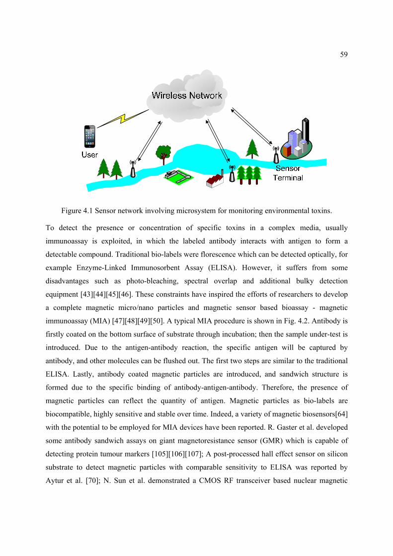
59
Figure 4.1 Sensor network involving microsystem for monitoring environmental toxins.
To detect the presence or concentration of specific toxins in a complex media, usually
immunoassay is exploited, in which the labeled antibody interacts with antigen to form a
detectable compound. Traditional bio-labels were florescence which can be detected optically, for
example Enzyme-Linked Immunosorbent Assay (ELISA). However, it suffers from some
disadvantages such as photo-bleaching, spectral overlap and additional bulky detection
equipment [43][44][45][46]. These constraints have inspired the efforts of researchers to develop
a complete magnetic micro/nano particles and magnetic sensor based bioassay - magnetic
immunoassay (MIA) [47][48][49][50]. A typical MIA procedure is shown in Fig. 4.2. Antibody is
firstly coated on the bottom surface of substrate through incubation; then the sample under-test is
introduced. Due to the antigen-antibody reaction, the specific antigen will be captured by
antibody, and other molecules can be flushed out. The first two steps are similar to the traditional
ELISA. Lastly, antibody coated magnetic particles are introduced, and sandwich structure is
formed due to the specific binding of antibody-antigen-antibody. Therefore, the presence of
magnetic particles can reflect the quantity of antigen. Magnetic particles as bio-labels are
biocompatible, highly sensitive and stable over time. Indeed, a variety of magnetic biosensors[64]
with the potential to be employed for MIA devices have been reported. R. Gaster et al. developed
some antibody sandwich assays on giant magnetoresistance sensor (GMR) which is capable of
detecting protein tumour markers [105][106][107]; A post-processed hall effect sensor on silicon
substrate to detect magnetic particles with comparable sensitivity to ELISA was reported by
Aytur et al. [70]; N. Sun et al. demonstrated a CMOS RF transceiver based nuclear magnetic

60
resonance system for the detection of biological objects [108]; Wang et al. [73] [109]proposed a
resonent frequency based handheld platform for magnetic beads detection and claimed a
sensitivity of single individual bead. Among these magnetic sensors, planar microcoil based
sensor shows more advantages in biomedical/microelectronic hybrid microsystems, since it is
compatible with mainstream mass-producible processes and the microcoil per se can be used as
magnetic field source to activate magnetic particles, avoiding external permanent magnets.
Additionally, the LC oscillating tank based shift frequency counting technique allows for an
accurate measurement in wide range with low power consumption. Therefore, it has the greatest
potential for portable point-of-care diagnostics applications.
Figure 4.2 Flow chart for a typical magnetic immunoassay: a) antibodies are patterned on bottom
surface of substrate; b) under-test sample solution is introduced, specific antigens will be
captured due to antigen-antibody reaction, and other molecules in solution are flushed out; c)
magnetic beads labeled antibodies are injected, a sandwich structure is formed. Superfluous
beads that are not bound are flushed out. Finally the amount of magnetic beads that can be
detected by sensor reflects the amount of antigen.
Although the aforementioned biosensors can achieve high sensitivity and miniaturization, they
are still confined to laboratory due to several challenges. First, due to the combination of

61
microfluidic structures with microelectronics on the same silicon die, great care needs to be taken
when treating the planar coil sensor surface for functionality to avoid damages, and the treatment
usually requires clean room environment, uses non-standard processes and takes several days,
thus it’s hard to meet our need for real-time detection. Second, the bonding of silicon die with
low-cost microfluidic structures increases the testing cost, because the direct contact of sensor
with liquid samples makes silicon chip disposable. Last, once bonded to silicon die, microfluidic
structure doesn’t allow sequential reconfiguration to adapt for different applications. To
overcome these drawbacks, we propose a scheme that exploiting reusable electronic device and
disposable microfluidic structure, whereas microcoil array is their connection but not in direct
contact with analytes. Electronic device consists of integrated detection circuit, off-chip planar
microcoil as sensor and microcontroller, whereas microfluidic structure takes advantage of
standard biomedical components. In this manner, the whole detection time is reduced because
sensor treatment and many other preparation steps are eliminated. Moreover, it is more economic
for repeatable testing and it allows for a flexible reconfiguration of microfluidic structures for
specific application.
For the sake of designing a high performance, low-cost and easy-to-use microsystem platform,
several issues need to be respected. The most critical issue is how to design the front-end
microcoil and sensing circuit, as it determines the sensitivity of detection. Additionally, the
packaging technique is also very important as a robust biological interface will definitely
facilitate the device setup and testing process, thus shorter detection time and more reliable
results can be achieved. The architecture of our proposed microsystem platform is depicted in Fig.
4.3. It consists of four main parts, namely, the microfluidic structure, the microcoil sensor array,
the CMOS application specific integrated circuit (ASIC) and microcontroller. All of them are
mounted on a small PCB board which is possible for any other necessary extension functions.
The microcoil sensor array is the connection between microfluidics and microelectronics. With
the incorporation of microelectronic circuits, the sensing signal is processed and the local
magnetic field is possible to be reconfigured, thus various functions can be achieved. Be aware
that the sensor substrate may vary depending on different implementations and thus leads to
different integration mode. For example, if microcoil sensor substrate is silicon, it is usually
preferred for microcoil to share the same substrate with CMOS chip to achieve a better
integration, whereas when substrate is other materials for example polymer, we connect it with
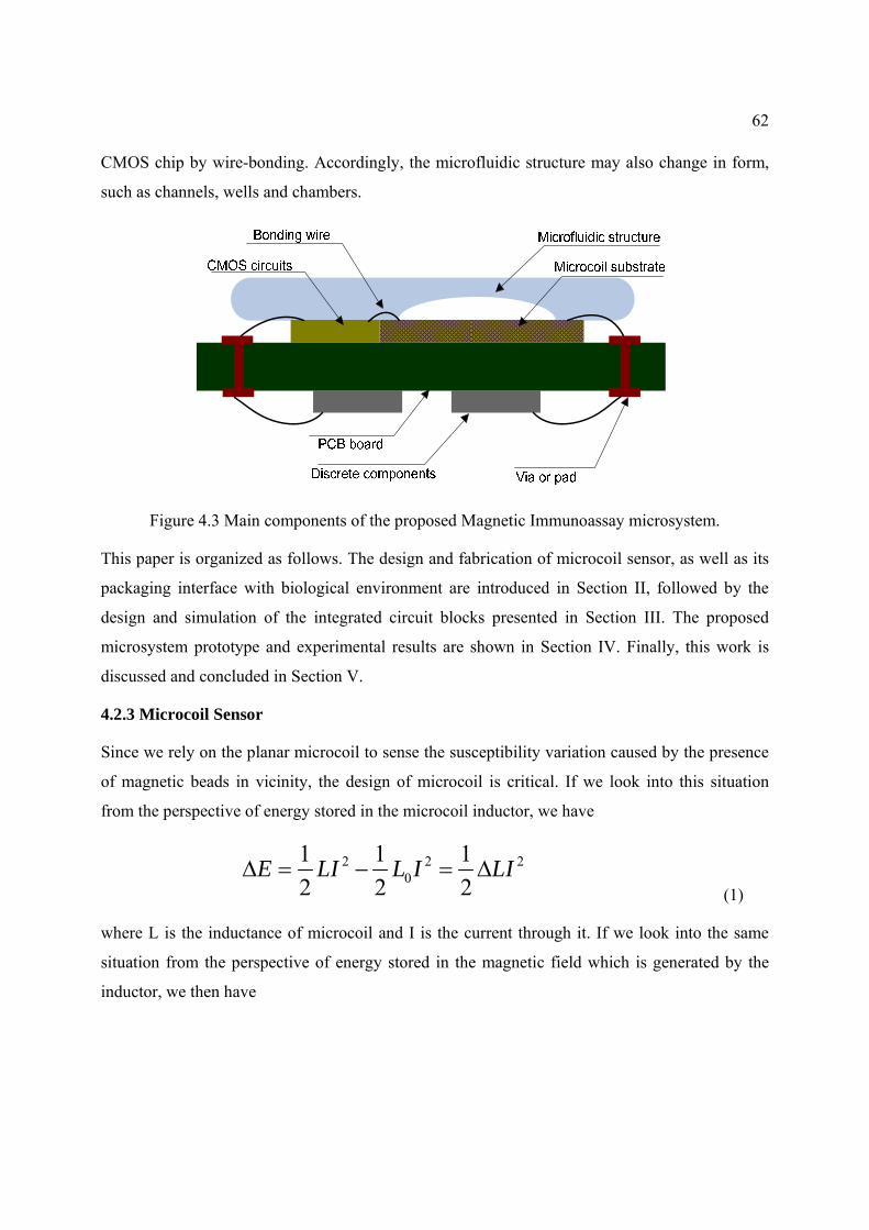
62
CMOS chip by wire-bonding. Accordingly, the microfluidic structure may also change in form,
such as channels, wells and chambers.
Figure 4.3 Main components of the proposed Magnetic Immunoassay microsystem.
This paper is organized as follows. The design and fabrication of microcoil sensor, as well as its
packaging interface with biological environment are introduced in Section II, followed by the
design and simulation of the integrated circuit blocks presented in Section III. The proposed
microsystem prototype and experimental results are shown in Section IV. Finally, this work is
discussed and concluded in Section V.
4.2.3 Microcoil Sensor
Since we rely on the planar microcoil to sense the susceptibility variation caused by the presence
of magnetic beads in vicinity, the design of microcoil is critical. If we look into this situation
from the perspective of energy stored in the microcoil inductor, we have
2 2 20
1 1 12 2 2
E LI L I LIΔ = − = Δ (1)
where L is the inductance of microcoil and I is the current through it. If we look into the same
situation from the perspective of energy stored in the magnetic field which is generated by the
inductor, we then have

63
'0
2 20
2 2
0 0
1 12 2
[| | (1 ) | | ]2
| | | |2 2
P
P
V
PV
E H Bdv H B dv
H H dv
B dv B V
μ χ
χ χμ μ
Δ = ⋅ − ⋅
= + −
= ≈
∫∫∫ ∫∫∫
∫∫∫
∫∫∫ (2)
where pV is the volume of magnetic particles, χ is the magnetic susceptibility per unit volume and
0μ is the magnetic permeability in free space. Therefore, LΔ can be computed by equating (1) and
(2)
2
20
| |p
BL VI
χμ
Δ ≈ (3)
From (3) we know the inductance variation of microcoil caused by magnetic beads is
proportional to magnetic susceptibility χ , the magnitude of magnetic flux density B , and
inversely proportional to the current I through the inductor. Noting that the above computing is
under the assumption that the magnetic bead is so small that it does not affect the overall
magnetic field intensity H , meanwhile B is first-order proportional to I [25] [26]. Therefore, the
inductance variation of a microcoil is linear to the quantity of magnetic beads in vicinity, because
a bigger quantity results in a bigger total volume pV . However, to design a linear microcoil
sensor in realistic, some other parameters also need to be considered.
The first consideration is the influence of parasitic capacitance. At frequencies below a few GHz
[25], the presence of the magnetic particles leads to an increase in the magnetic susceptibility of
the medium in vicinity of microcoil, meanwhile, the self resonant frequency and quality factor of
a microcoil are dependent on the self inductance L and serial resistance Rs, as well as the
parasitic capacitance between wires Co, the parasitic capacitance between wire and substrate Cox
and the substrate resistance Rsi, as shown in Fig. 4.4 (b). Regarding the complex media of under
test samples, the background biological particles in fluid could influence the parasitic capacitance
by changing the permittivity of media between wires, thus the relationship between self resonant

64
frequency and magnetic susceptibility is no longer linear even though the LΔ is linear to
magnetic susceptibility as indicated in (3), because the self resonant frequency is determined by
both the total inductance and parasitic capacitance. To avoid this issue, we can add a thin
isolation layer on top of microcoil to make sure that the magnetic beads are still in the strong
magnetic field region, but the fluid does not approach the gap between wires to change the
parasitic capacitance.
Figure 4.4 Planar microcoil as magnetic sensor: a) the concept of microcoil and magnetic
particles with toxins captured; b) high frequency equivalent circuit model; c) cross sectional view
of a microcoil showing the total magnetic field distribution; d) our fabricated microcoil with
inductance 210nH, DC resistance 0.65Ω and Q factor 75 at 200 MHz.
The second consideration is the uniformity of magnetic field generated by planar microcoil. Since
we aim for quantitative biomedical measurement, we need to make sure that the sensor can
differentiate less magnetic beads in strong magnetic area and more magnetic beads in weak
magnetic area, because these two cases could result in same influence to the total inductance
variation of microcoil. Therefore, we need to design a microcoil with relatively more uniform

65
magnetic field within the sensing area. Fig. 4.4 (c) shows the cross sectional view of the Finite
Element Analysis (FEA) result of the magnetic field generated by a microcoil. If we define the
center of a microcoil as origin, the plane that is parallel to the surface of microcoil as x-y plane,
and the plane that is perpendicular to x-y plane is z plane, then it is worth noting that the
uniformity of magnetic field in x-y plane varies over z direction[110]. It means the distance from
sensor surface to the surface that magnetic beads are attached needs to be considered. Generally,
there are two schemes: the first scheme is to employ only the center area of the sensor as in [26],
which provides relatively uniform magnetic field. However, this scheme suffers from a reduced
sensing area, because most of the sensor surface is wasted. Additionally, an extra post-fabrication
step for aligning the microfluidic and sensor positions is required, it is quite challenging because
the consistency for multiple sensors packaging is difficult to be guaranteed especially when
microcoil size is small. The second scheme is to employ the sensing area at higher distance to
sensor surface in z direction. Due to the better uniformity, it can achieve a bigger sensing area.
However, there is always a tradeoff between uniformity and sensitivity, because a further
distance means a weaker magnetic field. Therefore, the thickness of isolation layer should be
carefully designed while respecting the FEA simulation results. Since the effective magnetic field
region is comparable to the layout region of a microcoil in x and y direction, but decreases
sharply in z direction, as shown in Fig. 4.4 (c), the isolation layer between metal and microfluidic
should be as thin as possible while the magnetic beads locate in the uniform magnetic field area.
This point is very meaningful, because on one hand when the sensor is fixed, we can control the
uniformity and detection area by changing the thickness of isolation layer, on the other hand
when the isolation layer is fixed, for example when we use commercial microfluidic components,
we can change the design of sensor to make sure the bottom surface of microfluidic structure
locates in the appropriate magnetic field region.
In addition to the above two considerations, the dimension of microcoil also need to be discussed.
Generally, it can be divided into two categories – single magnetic particle detection using
comparable size microcoil as sensor and mass-coverage sensors with active areas of hundreds of
square microns to millimeters. Obviously, in practical measurement, it is more significant for
providing statistical counting of a large number of magnetic labels in bioassay, instead of just a
positive or negative output. Therefore, we employ moderate size microcoil that is capable of
detecting a series of magnetic beads with different densities. In our prototype, our fabricated

66
microcoil array as shown in Fig. 4.4 (d) exploited a process that the substrate is a very thin all-
polyimide composite of polyimide film bonded to copper foil. It’s a low cost and mass producible
product provided by Pyralux®. In this technology, the dielectric thickness is only 100 µm, but
copper thickness is 35 µm. Compared with the metal thickness for silicon substrate which is
usually below 3µm, the thicker metal in this process can tolerate a higher current which leads to
generate a stronger magnetic field. Moreover, thicker metal results in less resistance and higher Q
factor for the inductor, which is extremely important for high frequency noise reduction.
Meanwhile, the ultra thin dielectric layer results in less magnetic energy loss and better heat
dissipating. The minimum wire width and space allowed by the design rules are 50 µm and 75µm,
respectively. The sensing area is designed to be comparable with the size of each well of standard
96 wells microplate used in biomedical experiments. Another significant advantage for this
technology is that we can make some pads on the back side of the substrate, thus the integration
of microfluidics and electronics will be easier and the miniaturization of device is possible
because all the off-chip components can be integrated on the backside of sensor board. The
achieved inductance is around 210nH-212nH, DC resistance is 0.65Ω-0.7Ω and Q factor is about
75 at 200MHz, the variation is due to non-symmetric layout and should be normalized and tuned
in application.
Our fabricated microcoil sensor is compatible with various microfluidic structures, such as
channels, wells and chambers, however, most of the conventional interfaces to connect electrical
sensor with biological sample tend to bring extra errors during experiments, due to many
inevitable issues in non-standard process, such as the unsmooth surface and leakage. In order to
increase the accuracy of sensing and minimize the errors result from non-standard packaging, as
well as to take advantage of the mature experimental techniques of traditional ELISA, we apply
standard 96 wells microplate [70] as the container of under-test sample. To note that using
common 96 wells microplate suffers from low detection sensitivity, because the thickness of
bottom plate is usually over 1mm, thus the distance from magnetic beads to microcoil exceed the
effective range of strong magnetic field generated by microcoil. Fortunately, special microplate
with ultra thin bottom can be employed. In our experiments, we used Corning® 96 well special
optics flat clear bottom microplate, whose bottom plate thickness is only 127 µm. The fabricated
microcoil was designed to accommodate the size of each well of microplate and the thickness of
bottom plate, so that the detection area can be maximized and magnetic field uniformity can be

67
improved. Moreover, benefiting from the separation of reusable electrical environment and
disposable biological environment, the consumed material in each testing is further reduced
whereas more parallel data can be collected.
4.2.4 Integrated CMOS Chip Design
Our integrated circuits were fabricated in CMOS 180nm technology provided by TSMC, the
circuit blocks are shown in Fig. 4.5. The main detection circuit is based on a LC tank oscillator in
which the above introduced microcoil sensor plays the role of inductor and voltage controlled
transistors are used as capacitors. The oscillating signal is then shaped to frequency countable
digital signal through signal conditioning circuit, and the final output is processed by an off-chip
microcontroller (MCU) MSP430. A bidirectional current source is used to supply the microcoil a
high current for generating strong magnetic field, so as to attract the magnetic beads in solution to
the bottom of microplate for a higher interaction ratio between antigen and antibody, whereas
different microcoil can be selected by multiplexer. Additionally , for the sake of maintaining a
proper temperature range to assure the viability of bioparticles, and to reduce the performance
degradation of detection circuit due to temperature drift, two proportional-to-absolute
temperature (PTAT) sensors are implemented on chip to monitor the ambient temperature.
Figure 4.5 Block diagram of the achieved CMOS chip.

68
One of the key circuits in our designed CMOS chip is the cross coupled LC oscillator and the self
biased amplifier as buffer. As shown in Fig. 4.6(a), transistors M1-M4 form the cross coupled
structure so as to provide the negative Gm to cancel the loss in the LC tank as well as a DC bias
for following stage; M5-M9 form the self-biased amplifier to provide additional gain thus no
matter the oscillator works at voltage limited mode or current limited mode[111], the magnitude
of output signal will always be significant; M10-M11 forms the output buffer. The frequency of
oscillating signal depends on the LC tank and directly reflects the quantity of magnetic particles
in media. The signal is then shaped by the self-biased circuit and buffered out for frequency
counting. The self biased circuit can also amplify the signal before the LC tank oscillates stably,
thus facilitates the high-precision frequency counting. If we regard the microcoil as the
inductance of a LC tank, the presence of magnetic beads will increase the effective inductance, so
the output frequency changes to
12
000 0
1
0 00 0 0
1 (1 )2 ( )
1( ) (1 )2
20
n
n
Lf fLL L C
L Lf fL L
π−
=
Δ= = +
+Δ
⎛ ⎞− Δ Δ⎜ ⎟≈ = −⎜ ⎟⎝ ⎠
∑ (4)
where 0L , 0C and 0f are the original inductance, capacitance and oscillation frequency,
respectively. After first-order Taylor series approximation, we know the output frequency is
almost linear to inductance variation hence linear to magnetic susceptibility according to (3). If
we can measure the frequency shift in small intervals, we will get the corresponding inductance
variation caused by the presence of magnetic beads.
The transient time simulation result of signals from LC tank and final output are shown in Fig.
4.6 (b). Inductance and capacitance used in simulation were 210 nH and 4.7 pF, respectively. It
indicates that the irregular analog oscillating signal can be shaped to countable digital circuit
even when it works at voltage limited mode. Therefore, fast and wide range detection can be
achieved simultaneously.

69
Figure 4.6 Schematic of cross coupled LC oscillator and self biased buffer circuit and simulation
results: a) schematic; b) transient simulation result; c) phase noise simulation results.

70
Sensitivity is usually the most important factors to evaluate the performance of a sensor. From (4)
we know that the sensitivity of measurement mainly depends on the original sensor inductance
and oscillating frequency. Smaller inductance and higher oscillating frequency result in higher
sensitivity. However, on-chip minimized microcoil usually requires post fabrication process for
surface treatment to accommodate microfluidic and complicated alignment for precise placement
of liquid on sensor. Furthermore, minimized sensor has a smaller uniform detection area, thus it
has a lower capacity to contain detectable targets and higher risk of random error caused by non-
specific binding. In order to achieve a bigger area for linear quantitative detection, choosing
appropriate size microcoil while scarifying some sensitivity is acceptable. After all, accuracy is
another important factor to evaluate the sensor in addition to sensitivity, for example, single
magnetic bead detection in MIA experiment can not necessarily be guaranteed to be accurate.
Considering these facts, the size of sensor is better to be determined by the size of container for
biomedical reagents, particularly when our aim is to design a portable and easy-to-use device.
Another important consideration is noise, as it will affect both sensitivity of accuracy of the
sensor. Basically, in biomedical microsystem, noise can be divided into electrical noise and
biomedical noise. Electrical noise needs be minimized through circuit design whereas biomedical
noise can be minimized through exploiting better testing protocol. For our proposed oscillator
circuit, phase noise is an important factor to evaluate its performance, as it indicates the stability
of the circuit, especially in the inductance based measurement for which the main tone is variable.
Noise source may cause both magnitude and frequency of oscillation to vary, thus lead to
inaccurate frequency counting. Previous research on LC oscillator[26] shows that the noise floor
of an oscillator circuit is proportional to the ratio of L/Q, which is determined by the design of
microcoil, and usually can be predicted in a reasonable range when the area is fixed for planar
coil. In the cross coupled LC oscillator circuit, we can minimize the upconversion of 1/ f noise
by tuning the relative widths of the PMOS and NMOS transistors. Through exploitation of
symmetry in this manner, the 31/ f noise can also be reduced. Furthermore, the bridge like
arrangement of the transistors quad allows for greater signal swings, compounding the
improvement in phase noise[112]. As a result of respecting all of these factors, the simulation

71
result in Fig. 4.6(c) reveals that at an offset of 500 KHz and 10 KHz, the phase noise of our
prosed circuit is -143.0dBc/Hz and -105.8dBc/Hz, respectively.
Biomedical noise generally means how well the reactions between antigen and antibody are.
Owing to the fact that during MIA the binding between antigen and antibody is not necessarily
one to one, the nonlinearity issue could be severe because our final quantitative detection result is
reflected directly by the amount of magnetic beads. The best solution is to make sure the
complete reaction by introducing large amount of antibody coated magnetic beads into reaction
area. In practical MIA testing, magnetic beads are randomly dispersed in the original solution
under test but the antigen-antibody structure forms only at the bottom plate. If the magnetic beads
which are supposed to bond to all the antigen are not fully bonded, it will lead to nonlinear result.
Using a high density magnetic beads solution may result in a more complete interaction, but the
superfluous magnetic beads tend to form chain or clutter by self-interaction[83], furthermore,
high density magnetic beads increase the risk of residue after washing steps, which will in turn
lead to nonlinearity. Our proposed solution is that the same microcoil is designed to be switched
between manipulating mode and detecting mode by a multiplexer as shown in Fig. 4.5. The
detection procedure is as follows: firstly, microcoil is switched to manipulating mode to attract
the magnetic beads in vicinity, after a short time, when most of the magnetic beads are attracted
to the bottom of liquid and antigen-antibody interaction is fully completed, then the microcoil is
switched off and the extra magnetic beads are re-dispersed into the solution and washed out of
the wells of microplate; finally the corresponding microcoil is switched to detecting mode,
waiting for the frequency counting. In this manner, a relatively lower density of magnetic beads
solution can be employed to achieve a more complete interaction without the assistance of
external magnets.
In order to generate a strong and relatively uniform magnetic field at the bottom of microplate to
attract the magnetic beads, we employ a current source with high current output capacity. The
current source we use in our design is an H-bridge circuit with current sink as shown in Fig. 4.7.
The current direction can be changed depending on the on and off of transistors pair “1&4” or
“2&3”, and current capacity can be controlled by current sink. Different microcoils can be
selected by a low on-resistance multiplexer. Post layout simulation results in Fig. 4.7 reveal that
when applied a direction control signal with frequency 200 KHz, the current through coil can
vary between ± 50mA, with each step about 15mA. Intuitively, higher current may result in

72
higher attraction ratio, but in practical experiment, the value of current needs to be optimized by
observing the final measurement. In fact, coil may get saturated when increasing current no
longer increase the attraction ratio significantly, in this situation, the extra heat will level up the
noise floor of the whole system instead.
Figure 4.7 Bidirectional current supply circuit: a) schematic and b) post-layout simulation result.
Since we need a big current to drive the coils, a very low on resistance for the transistors used in
the above circuits is required to reduce the total power consumption. We chose face to face
PMOS and NMOS transistors pair as digital controlling circuit to select different microcoils.
Therefore the main resistance is from the on resistance of transistors pair. Main factors that affect

73
Ron are input voltage, gate width, channel length and temperature. Basically Ron can be
expressed as
1
( )( )on
n OX In T
R WC VCC V VL
η=
− − (5)
From (5), we know bigger width and minimum length lead to a lower Ron. Furthermore, in
practical circuit design, paralleled PMOS and NMOS transistors are often applied to reduce Ron.
Nevertheless, there is a constant trade-off between the on-resistance and the parasitic
capacitances of this transistor pair. If W is chosen to be too small, large Ron will degrade the
overall quality factor of the tank. On the other hand, if W is chosen to be too big, the excessive
parasitic capacitances will result in nonlinearity of LC tank, because the parasitic capacitance of a
transistor is proportional to the product of W and L. Thus system simulation needs to be
conducted after layout to find the most appropriate value. In our design, W=500 um and L=0.18
um are finally employed.
For the reason that the employed oscillator is actually free running, its performance is dependent
on ambient temperature, and usually the oscillating frequency shifts to a lower frequency when
ambient temperature increases[113], however, the implementation of current source to drive
microcoil as magnetic source may lead to heat dissipation thus increase the ambient temperature.
In order to increase the stability of LC oscillator and make sure that the whole microsystem is
always maintained in a safe temperature range for bioparticles, we integrate a PTAT sensor on
chip to monitor the system temperature and minimize the errors due to ambient temperature. The
schematic and concept of temperature control is shown in Fig. 4.8 (a). The output voltage of
PTAT sensor can be sampled by the integrated analog to digital converter (ADC) in MCU, and
then the temperature will be analyzed and compared with the preset value, which is a 5 range.
If the temperature is still within the safe range, MCU will control the current source through
multiplexer to drive microcoil array to generate magnetic field, otherwise the magnetic field is
cut off. Two PTAT sensors are on the same chip, for calibration and comparison purpose, to
ensure the accuracy of temperature monitor. From Fig. 4.8(a), we know the relationship between
the final output voltage and temperature can be expressed as
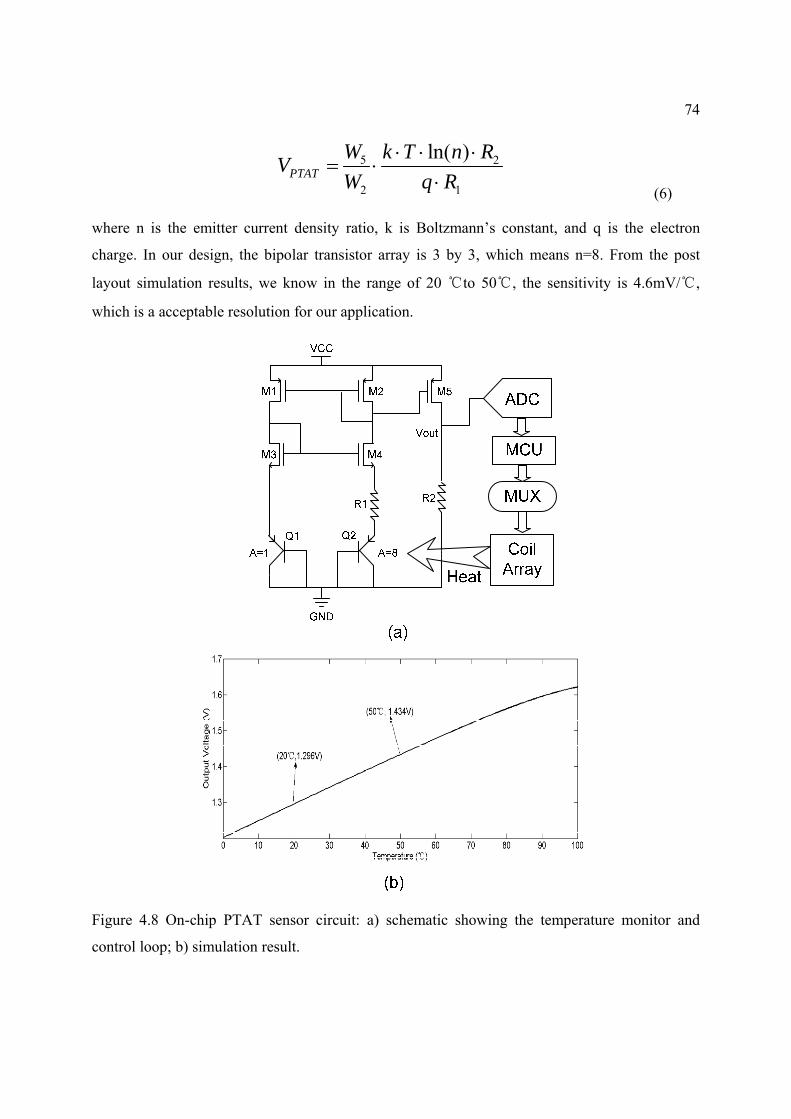
74
5 2
2 1
ln( )PTAT
W k T n RVW q R
⋅ ⋅ ⋅= ⋅
⋅ (6)
where n is the emitter current density ratio, k is Boltzmann’s constant, and q is the electron
charge. In our design, the bipolar transistor array is 3 by 3, which means n=8. From the post
layout simulation results, we know in the range of 20 to 50, the sensitivity is 4.6mV/,
which is a acceptable resolution for our application.
Figure 4.8 On-chip PTAT sensor circuit: a) schematic showing the temperature monitor and
control loop; b) simulation result.
75
4.2.5 Microsystem Prototype and Experiments
For biomedical microsystems that need be scaled from laboratory to massive industrial
production, the design of microelectronic/microfluidic interface is also challenging in addition to
the design of biosensor and circuits, because a fine environment for bioparticles in terms of
temperature and humidity is not usually unwanted for electronic device. A superior interface will
facilitate the packaging procedure so that a fast setup can be realized whereas liquid leaking issue
can be eased. Beneficial from the separating of microelectronics and the microfluidic structures,
it is quite flexible to make different microfluidic structures such as channels, chambers and wells,
depending on specific application. In our testing, we exploited ultra thin bottom 96 well
microplate as the container of under test sample, compared with customized or manual made
container, it results in improved consistency, repeatability, and reduced possible defects. The
proposed complete MIA platform is shown in Fig. 4.9 (a). It is portable format, with reusable
electronic platform and disponsible microplate. Fig. 4.9 (b) shows the sensor board with a
microcoil array of 21 coils in total. It’s worth noting that the microcoil array can be easily scaled
up if a bigger amount of data analysis is required. Our designed CMOS chip was mounted on the
backside of the sensor board, whereas its micrograph is shown in Fig. 4.9 (d). This platform can
be further miniaturized by integrating all the off-chip components on the same substrate with
microcoil sensor to reduce the overall weight and cost, but the minimum size is limited by the
size of microplate as the sensor board has to accommodate the microplate.
We performed MIA experiments to measure the density of mouse IgG in the following procedure
according to manufacturer's instructions of all materials. During the whole measurement, the
temperature the microsystem is maintained roughly same using the scheme proposed in [114], to
guarantee the viability of bioparticles and performance of electrical components.
1/ The 96-well plate (Costar EIA plates, Lowell, MA) was incubated for overnight with 100μl per
well of goat Fc-specific anti-mouse IgG (Jackson Immuno Research, West Grove, PA) diluted by
PBS buffer (NaCl 137mmM, KCl 2.7mmM, KH2PO4 1.5mmM, N2HPO4 8.1mmM) at 10μg/ml.
As a result, a high density of anti-mouse IgG was planted on the bottom surface of plate wells.
2/ The antibody-coated microplate was washed three times with 200μl PBS for 5 minutes on a
shaker, before blocking the nonspecific site for 1 hour at room temperature (RT).

76
3/ Followed by three times washes, ten-fold serial dilutions of purified mouse IgG (Jackson
Immuno Research) from 1μg/ml to 100pg/ml were applied in triplicates for 2 hours incubation at
RT. Blocking buffer without mouse IgG was also added as negative control. As a result, mouse
IgG and anti-mouse IgG were bonded to together, and mouse IgG was guaranteed to be fully
bonded.
Figure 4.9 Prototype of the microsystem: a) The view of platform showing the setup of 96 wells
microplate, microcontroller board, LCD display and power supply circuits ; b) The sensor board
under the microplate; c) The backside view of sensor board showing the mount of our designed
CMOS chip; d)The micrograph of our designed CMOS chip.
4/ 5ml goat anti-mouse IgG coated magnetic beads (mean diameter 1.5µm) solution ( BipMag
Plus, Bang’s Laboratories Inc) were transferred to the centrifuge tube. By magnetically
separation, the solution was cleared and the supernatants were removed gently by pipette. The
particles were washed three times with the equal amount of wash buffer (PBS, 1% BSA, 0.1%
NaN3, 1mmM NaN2 EDTA, Bangs Laboatories, Inc) by resuspending the particles and removing

77
the supernatants. As a result, anti-mouse IgG coated magnetic beads solution was purified and
ready to be used.
5/ The plate was washed three times, and then 100 μl of 50 μg/ml solution prepared in step 4 was
added in each well and incubated for 2 hours at RT. As a result, antigen-antibody sandwich
compound were formed.
6/ Followed three times washing, plate was dried and placed on detection platform for measuring
the quantity of magnetic beads.
Figure 4.10 Experiments results: a) real time data record showing output frequency v.s. time; b)
extracted data showing frequency shift v.s. density of mouse IgG.

78
After all the above steps, each hole of 96 wells microplate was aligned on top of microcoil sensor
board, and the output frequency was sampled and recorded by row of the 96 wells microplate
from lowest to highest density. In between of each sampling with time gate 10s, the frequency
counting circuit was switched back to negative control group and revealed an original oscillating
frequency 195 MHz. The amplitude of noise floor, i.e. the frequency variability for control group,
is about 20 KHz. The real-time output frequency data recording is shown in Fig. 4.10 (a) , it
consists of over 1000 sampling dots. The extracted data is shown in Fig. 4.10(b), after filtering
out the unreliable data when switching the different coils. To minimize the influence of noise
floor and some unexpected random error, the results of each column of microplate, which
includes 12 holes, are averaged. The minimal density of 100pg/ml can be detected, but it has
already approached the limit of sensitivity, because the sampled data is very close to the noise
floor. When the density of mouse IgG is 10ug/ml, it seems that the saturation effect begins to
dominate, thus the sensor is not linear anymore. Some random errors happen during measuring
the output frequency, but it can be easily removed by programming algorithm in microcontroller.
To note that the x axis of Fig. 4.10(b) is in logarithmic scale, therefore, the relationship between
the shift frequency and density of mouse IgG is not directly proportional, although we have
theoretically proved that the shift frequency and the amount of magnetic beads have a relation
that is approximately linear. The reason is that the binding process of magnetic beads and
bioparticles is not linear. Due to the large size of magnetic bead (above 1 µm) compared with that
of IgG (below tens of nm), usually a single magnetic bead carries a large quantity of anti-mouse
IgG on the microsphere surface, but not all of these anti-mouse IgG can fully react with mouse
IgG, because the antigen-antibody compound are attached to a flat surface, instead of uniformly
dispersed in solution.
To double verify our measurement results, we also observed the transparent microplate under
microscope after MIA experiments as shown in Fig. 4.11, where magnetic beads are adhered to
the bottom as we expected, and the quantity of magnetic beads vary according to the density of
mouse IgG. To note that Fig. 4.11 only provides us a visual verification to the measurement
results, instead of an accurate counting of magnetic beads. The reason is that due to the large
detection area comparing to magnetic bead size, it’s not practical to manually count the total
number of magnetic beads in each well, especially for those wells with high density attachment.
Moreover, at low density, the binding of mouse IgG with anti-mouse IgG is not uniform, thus

79
multiplying the amount of magnetic beads in view by the total area of each well is not an accurate
counting method also. As a matter of fact, we observed that for the lowest density of mouse IgG
(100pg/ml), the total amount of attached magnetic beads on the bottom plate of well is in the
range of 20-30, which is close to the detection sensitivity limit of our sensor.
Figure 4.11 Microscopic view showing the attached different densities of magnetic beads in
different microplate wells, the corresponding mouse IgG added in wells are: a)1ng/ml; b)10ng/ml;
c)100ng/ml; d)10ug/ml.
From the experimental results, we find that at lower density of IgG, the main constraint to further
increase the sensitivity is the level of noise floor. We believe that high performance applying
TDC (Time-to-Digital-Convertor) circuit or PLL (Phase-Lock-Loop) circuit will further increase
the sensitivity but at the cost of higher circuit complexity and power consumption. Compared
with [115]in which a bulky solenoid coil oscillated at low frequency (hundreds of KHz) was used
to detect magnetic beads with low detection sensitivity ( 510 ) and [109]in which micro planar on
silicon coil oscillated at ultra high frequency (1.1GHz) was used to detect magnetic beads with
single bead sensitivity, our sensor works at middle frequency (160MHz-200MHz), with moderate
sensitivity but bigger detection area and reliable results due to the high linearity in wide density

80
range. Additionally, the employment of our off-chip coil sensor makes the platform compatible
with traditional biomedical components which is easier to use, thus better for widespread
deployment.
4.2.6 Conclusion
In this paper, we introduce the implementation of a microsystem platform for detecting toxins
and pathogens in food and water. Magnetic microbeads are used as bio-labels of toxins and
detected through measuring the susceptibility variation of media. We focus on the design of
front-end microcoil and sensor circuit, as well as the packaging techniques for a robust biological
interface. The detecting scheme was analyzed and simulated to verify our concept firstly, whereas
testing results with mouse IgG and anti-mouse IgG are also reported. The concept of separating
microfluidic structure with microelectronic part brings several advantages such as low cost, easy-
to-use and flexible reconfiguration. To further improve the stability and reliability, we use
multiplexer to switch the microcoil to manipulating mode in order to concentrate the magnetic
beads before sensing. Experimental results show that mouse IgG with a minimum density of
100pg/mL can be detected, which is a comparable sensitivity to conventional optical ELISA. Our
proposed device is a good candidate to replace the conventional ELISA equipment in terms of
cost and usability, and it is also well suited to be used for tracking and positioning magnetic
labels in point of care diagnostics.
Acknowledgment
The authors would like to acknowledge the support from ReSMiQ, NSERC and CMC
Microsystems. The authors also want to thank Rejean Lepage and Laurent Mouden for their help
in using the hardware and software of Polystim Lab, and Nan Li for his constructive suggestion.

81
CHAPTER 5 A NOVEL BIO-MEMS CHIP FOR MAGNETIC BEADS
APPLICATIONS
5.1 Introduction
Although various LoCs for magnetic particles manipulation have been reported, integrating
microfluidic and electromagnets on a single chip is still challenging, due to the lack of reliable
fabrication techniques. The current devices are exploiting electromagnets chip plus post-
fabricated microfluidic structures or microfluidic chip plus external electromagnets, while the
consistency and repetition of the devices are hard to be maintained. Thus, a mass producible
monolithic chip integrating microfluidic structures and electromagnets is desirable.
As for the design of planar microcoil array, some previous studies only exploited simple
geometrical electromagnets or individual coils, whereas the optimization of individual microcoil
design for particular application and the coordination of multiple coils were often neglected.
Consequently, power consumption and manipulating efficiency cannot be well balanced.
Therefore, we need to investigate the geometry of individual microcoil to get a higher
performance and take into account the coordination of multiple microcoils to achieve a higher
manipulating efficiency.
In this chapter, we introduce a novel monolithic microfluidic chip from design, simulation to
experimental results. It takes advantage of the commercial MetalMUMPs process, from which
both the top electromagnetic and bottom microfluidic structures can be achieved from the same
fabrication process. Investigation on multiple coils cooperation is conducted by modeling and
simulation in FEA software, for the sake of achieving higher efficiency and bigger trapping area.
Additionally, we introduce a novel method to introduce micro scale fluid to chip, without using
the conventional microtubes. This method facilitates the device testing and avoids the liquid
leaking issue as well. The following section is the reproduction of an article published in Journal
of Microelectronic Engineering, Volume 128, 5 October 2014, Pages 1-6, ISSN 0167-9317.
82
5.2 A BioMEMS Chip with Integrated Micro Electromagnet Array towards Bio-particles
Manipulation
5.2.1 Abstract
We propose in this paper the design and implementation of a novel BioMEMS chip towards the
manipulation of magnetic micro/nano particles. Our proposed device integrates a planar
microcoil array and a microfluidic structure on a single chip, without any post-fabrication process.
Meanwhile, a multiple coil cooperation scheme is studied from simulation by Finite Element
Software and applied in application to increase the manipulation efficiency. Taking advantage of
computer-aided microplotter to introduce microfluidics to the chip, the traditional microtubes and
syringe pump are avoided. Hence, this chip is compact, low-cost and mass-producible.
Experiment is performed using antibody coated magnetic particles with mean diameter 1.5µm,
and the results reveal that this chip can achieve a high efficiency with trapping rate over 90%
while consuming a current of 40 mA, thus it has a great potential in bio-particles manipulation
for point of care diagnostics.
Keywords: Bio-MEMS chip; integrated electromagnets; planar microcoil array; magnetic
particles; manipulation.
5.2.2 Introduction
Magnetic micro- and nano- particles have been widely used in biomedical applications as labels
or carriers of bioparticles, such as DNA, proteins, and cells [116][117][118][119]. These
magnetic particles are actually superparamagnetic beads, and can be manipulated by permanent
magnets or electromagnets. In practical application, planar microcoil array is usually preferred in
bio-MEMS applications due to the flexible control of magnetic field, greater scalability and better
compatibility with mainstream microfabrication process [120][121][122]. With the cooperation of
external control circuit, magnetic particles in microfluidics can be programmably activated,
guided, trapped or sorted by planar microcoil array, to accomplish different biomedical
applications.
Although various BioMEMS chips for magnetic particles manipulation have been reported,
integrating microfluidic and electromagnets on a single chip is still challenging, due to the lack of
reliable fabrication techniques. The current devices are either electromagnets chip plus post-

83
fabricated microfluidic structures [56][87] or microfluidic chip plus external electromagnets [91],
while the consistency and repetition of the devices are hard to be maintained. Thus, a mass
producible monolithic chip integrating microfluidic structures and electromagnets is desirable.
As for the design of planar microcoil array, some previous studies only exploited simple
geometrical electromagnets or individual coils [61][92], whereas the optimization of individual
microcoil design for particular application and the coordination of multiple coils was often
neglected [123][124]. Consequently, power consumption and manipulating efficiency cannot be
well balanced. Therefore, we need to investigate the geometry of individual microcoil to get a
higher performance and take into account the coordination of multiple microcoils to achieve a
higher manipulating efficiency.
In this paper, we introduce a novel monolithic microfluidic chip from design, simulation to
experimental results. It takes advantage of the commercial MetalMUMPs process, from which
both the top electromagnetic and bottom microfluidic structures can be achieved from the same
fabrication process. Investigation on multiple coils cooperation is conducted by modeling and
simulation in Finite Element Analysis (FEA) software, for the sake of achieving higher efficiency
and bigger trapping area. Additionally, we introduce a novel method to introduce micro scale
fluid to chip, without using the conventional microtubes. This method facilitates the device
testing and avoids the liquid leaking issue as well.
5.2.3 Design and Fabrication
For our proposed device, the magnetic particles in microfluidic are activated and manipulated all
by the magnetic field generated by microcoil array, whereas no external permanent magnets are
applied. Due to the higher scalability and easier layout, square spiral microcoil is usually
preferred. To get a better understanding of the working mechanism, we firstly discuss the
situation of magnetic particle in magnetic field.
When magnetic particles are in magnetic field, from Maxwell tensor equation, the force on an
unsaturated magnetic particle due to the applied magnetic fields is [125]
( )mag mF V H B= χ ⋅∇ (1)

84
where magF is the magnetic force on the bead, V is the volume of the bead, mχ is its magnetic
susceptibility per unit volume, H is the magnetic field intensity, B is the magnetic flux density
and
B Hμ= (2)
where μ is the permeability of the medium.
In orthogonal coordinate system, extending eq.(1) in x direction leads to
( )m x x xx x y z
B B BF V B B Bx y z
χμ
∂ ∂ ∂= + +
∂ ∂ ∂ (3)
Eq. (3) reveals that the magnetic force acting on a bead depends on the magnetic field intensity,
as well as magnetic field gradient. Since a spiral microcoil of multi-turn can be considered to be
composed of an equal number of concentric square loops of different lengths, the total magnetic
field is the sum of the magnetic field induced by each loop, and it can be obtained from the Biot-
Savart law:
02
ˆ4
Idl rB dBr
μπ
×= = ⋅∫ ∫
(4)
where 0μ is the magnetic constant; I is the current passing through wire; dl is a vector whose
magnitude is the length of the differential element of the wire, and whose direction is the
direction of current; r is the displacement unit vector, in the direction pointing from the wire
element to the point at which the field is being computed and r is the distance from the wire
element to the point at which the field is being computed. Eq. (4) reveals that, approximately, the
magnetic flux density generated by a coil is directly proportional to the current through it and
inversely proportional to its diameter (coil size). As the size of coil shrinks, it need less and less
current to generate the required magnetic field. Therefore, it can be concluded that following the
minimum metal width of fabrication process to design the coil will result in strongest magnetic
field.
Our proposed single chip electromagnet microfluidic hybrid system has been fabricated using the
MetalMUMPs process [126]. Although it is usually designed for general purpose electroplated

85
nickel micromachining of MEMS devices, such as RF structure, relays, and magnetic switches
[127], it can be used to create microfluidic structure, after taking into account the characteristics
of this process. Fig. 5.1 shows the main four steps during fabrication of metal structure and
microfluidic structure.
The main process features we utilize for the proposed device are:
1) Electroplated nickel (20 um) is used as the main coil structure. Compared with the metal
thickness of other processes, for example, CMOS process, the extremely thick metal can sustain a
stronger current thus generate stronger magnetic field.
2) Doped polysilicon (0.7 um) is used for resistors and cross-over electrical routing to achieve
double-layer spiral planar coil. On chip resistor helps for further integration and prevents the
possible over-current problem.
3) Silicon nitride 1 (0.35 um) and 2 (0.35 um) are used as electrical isolation layer for
microfluidic/metal and metal/polysilicon, respectively. Therefore no post-process isolation is
needed for biological operation.
4) Trench layer (25 um) is used as microchannel or microwells for microfluidics. Due to the high
aspect ratio, complicated microfluidic structure can be easily achieved.
We model and simulate the designed MEMS chip by both Coventorware and Ansys software,
and then finish the layout in Coventorware. The designed model is shown in Fig. 5.1 (e). The 4×4
microcoil array and microchannel are isolated by silicon nitride (0.7 um). Besides the above
mentioned advantages, this process provides a novel topological structure of microsystem. Most
of the previous work exploited the structure with electromagnets in substrate and microfluidic
structure on top of substrate. In those cases, some of the magnetic particles tend to adhere to the
bottom plate of channel after turning off the current supply, due to the gravitational force and
frictional force between particles and the rough substrate [128]. These forces can be neglected in
perfect microchannel whose inner surface is smooth, but have to be considered when the
microchannel fabrication processes are not able to produce smooth substrate surface or the
substrate material itself is not smooth. This issue can be highly eased by MetalMUMPs process,
because the electromagnets locate on top of microfluidic structure, hence, magnetic particles are
easier to be released and a more efficient manipulation of magnetic particles can be achieved.

86
Figure 5.1 Main fabrication flow used in this design: a) deposition and pattern of isolation oxide,
sacrifice oxide and nitride layer 1 and 2; b) deposition and pattern of metal layer(coil structure),
anchor metal layer(connection between polysilicon and metal) and polysilicon layer; c) removal
of oxide layer by HF solution to form the suspended structure; d) KOH silicon etching to form

87
the trench; e) top view of final device model in Coventorware to show the whole device and
microchannel.
5.2.4 Controllable Magnetic Field by Microcoil Array
We first investigate the magnetic field distribution for different geometrical microcoil. As a
matter of fact, magnetic field distribution is highly geometry dependent for a planar microcoil. In
a given area and consuming same current, different geometries could lead to different maximum
values of magnetic field as well as their distribution. Since magnetic particles always tend to be
attracted to the nearest maxima of magnetic field, we can estimate the distribution of trapped
magnetic particles by choosing the geometry of planar microcoils. For example, as indicated in
Fig. 5.2, coil 2&4 have their maximum magnetic field at the center with large gradient, whereas
coil 1&3 don’t have their maximum magnetic field at the center but exert relatively more uniform
magnetic field. In our application, we need to trap as many magnetic particles as possible on the
substrate surface uniformly, instead of attracting all the magnetic particles to the center to form
cluster, so we choose the design of coil 1 or 3 to achieve a more uniform and larger trapping area.
From Fig. 5.2, we also see that the maximum magnetic field in coil 1&3 are lower than that in
coil 2&4, therefore realizing a more uniform magnetic field is at the cost of higher current
consumption as we need a higher current to reach the same magnetic force to manipulate the
magnetic particles.
Figure 5.2 Total magnetic field flux density distribution for different geometrical planar
microcoils: a) planar coil models, each coil occupies an area of 450 um by 450 um, carrying a
current of 30 mA; b) corresponding magnetic field distribution on the z = 1 um plane.

88
We then investigate the magnetic field distribution of coil model 1 in z direction. The coil is
designed following the limitation of MetalMUMPs design rules. For each coil, the width is 8 um,
space is 8 um, outer diameter is 450 um, and inner diameter is 80 um. The outer terminal is
connected to a pad which is wire bonded to a standard package of integrated circuit; the inner
terminal is connected through polysilicon first and then to another pad. Since the microchannel
depth is 25 um, isolation layer is 0.7 um, we need to find out the minimum current to generate the
required magnetic field that is strong enough to attract the magnetic particles at the farthest
distance in the microchannel. In addition to magnetic force, magnetic particles experience
hydrodynamic force and gravitational force, where the latter can be neglected due to small size.
Figure 5.3 a) Total magnetic field flux density distribution on x-z plane where y=0; b) magnetic
flux density in x direction where z=25 µm.

89
From Stoke’s law, we know
6 ( )hydro bead bead fluidF R v vπ= η −
(5)
where beadv , fluidv , beadR and η are the particle velocity, microfluidic velocity, bead radius and
fluid’s viscosity, respectively. Taking into account Eq. (1), the magnetic force needs to be bigger
than hydrodynamic drag force. For a typical magnetic particle with radium 1 um, 3 210 Nm− −η ≅ ,
and 51.67 /v m s−= ( 1 millimeter per minute), we have hydroF = 0.314 pN. Substituting 0.314 pN
to Eq. (1), and assuming the magnetic susceptibility is 0.33 [129], we know the magnetic field
has to satisfy the below condition to attract the particle:
2 10.034B B T m−×∇ = (6)
As the magnetic field generated by a spiral coil is extremely nonuniform, the magnetic field
gradient is usually high enough, therefore, we are more concerned with the magnetic field density.
Empirical value of minimum magnetic field to attract magnetic particles is about 10 Gauss [20].
Simulation result from Fig. 5.3 (a) shows the cross sectional view of magnetic field distribution
when y=0 and then we found a current of 30 mA through our designed coil was able to generate
more than 10 Gauss on the plane where z=25 um, and the magnetic flux density in x axis is as
indicated in Fig. 5.3 (b). To note that the coil model is not strictly symmetrical thus the magnetic
field distribution is asymmetrical.
In addition to the individual behavior of coil, we model and simulate four coils to investigate
their cooperation. The aim is to control the magnetic field in microchannel by manipulating the
amplitude and direction of the current in four coils. We investigate the xy plane where z=10 um.
The simulation results of the total magnetic flux density B are shown in Fig. 5.4 (b), (c) and (d)
for different cases. It indicates that when the current directions in four coils are identical, the
magnetic field generated by each coil is confined within each coil’s layout region, whereas the
maxima of magnetic flux density are located at the border region of adjacent coils when the
current directions of adjacent coils are opposite. Therefore, if we take into account the current
intensity and direction at the same time, then different control logics can be combined to achieve
different magnetic field distribution in microchannel, leading to different biomedical applications,

90
such as trapping, mixing, separating and transporting of bioparticles. For example, trapping is to
generate a relatively steady magnetic field to immobilize magnetic beads; mixing is to generate
an unsteady magnetic field to attract and repel magnetic beads alternatively; separating is a
special application of trapping, while multiple targets are differentiated by their magnetability;
transporting magnetic beads is based on the position variation of maximum magnetic field…
Figure 5.4 Magnetic field distribution of coil array: a) Four-coil array model in Ansys. Width 8
um, space 8 um, outer diameter 450 um, inner diameter 80 um; b) applying current in four coils
with same amplitude and direction, mode AAAA; c) applying current with same amplitude but
opposite direction for adjacent coils, mode ABAB; d) applying same amplitude current to four
coils but with same direction in the top two and opposite direction to the bottom two, mode
AABB; e) x directional magnetic field distribution, mode ABAB; f) z directional magnetic field
distribution, mode ABAB. (A and B represent the opposite current direction; figure b, c and d
share the top legend, whereas e and f share the bottom one).

91
It is worth noting that the aforementioned simulation results were discussed in terms of total
magnetic flux density, whereas for some applications, directional magnetic flux density should be
more emphasized. For example, when magnetic particles are located away from the microcoil
surface plane in the perpendicular direction, the z directional magnetic field dominates in the
process of attracting them to the microcoil. On the other hand, when we want to transport
magnetic particles that are located on the border of two microcoils to the adjacent microcoil, the x
or y directional magnetic field contributes more. Fig. 5.4 (e) and (f) shows the directional
magnetic field distribution of the same microcoil array in Fig. 5.4 (a). We can see that the
magnetic force exerts different directions on magnetic particles at different positions. Due to this
reason, magnetic particles are prone to rotating during manipulation process, especially when
they move across different regions of a microcoil.
5.2.5 Experiments
The fabricated chip and experiment setup are shown in Fig. 5.5. The device is firstly placed on
the platform of SonoPlot® GIX Microplotter, with the external current supply and control
circuits. The Microplotter uses controlled ultrasonics to spray fluid in a noncontact manner with
camera monitor. It is very suitable for high resolution, high throughput microfluidic applications.
After liquid is delivered into the inlets of our MEMS chip, we then manipulate the magnetic
particles in the fluid by controlling the current in microcoil array. The motion of liquid in a
microchannel relies on the pressure from the wedge shaped inlet, from which the continuously
sprayed liquid pushes the liquid in microchannel to move. Be aware that this method is not suited
for all microchannels, especially for microchannels with small dimensions, because the pressure
may not be high enough to overcome the surface tension of water. The use of microplotter
facilitates the introduction of microfluidic to the chip, thus facilitates the whole testing, by
avoiding installing hand-made inlet/outlet tubes and syringe pump for fluid. Meanwhile, the
microplotter can be programmed for multiple chips use, thus it can shrink the time for mass
production testing.

92
Figure 5.5 Micrograph of MEMS chip: a) microcoil and bonding wires; b) inlet/outlet of
microfluidic; c) micropipette absorbing liquid containing magnetic particles; d) micropipette
dispensing liquid from inlet; e) magnetic particles near the outlet of microchannel.
To test the performance of our device, we use magnetic particles with goat anti-mouse IgG
antibody attached. The magnetic particles actually contain superparamagnetic nano particles
inside and polymer shells outside, thus exhibit almost the same magnetic behavior with
superparamagnetic particles. The mean diameter of magnetic particles is 1.5µm, original
concentration is 1mg/mL and it is purchased from Bangs Laboratories. Before performing the
experiments, the original magnetic particles solution is firstly filtered by permanent magnets to
make sure that all the particles in solution are magnetically functional, and then the filtered
solution is diluted by deionized water to the density of 100ng/µl for use.

93
Figure 5.6 Experimental results showing the normalized trapping ratios versus current
consumption for single, double and triple activated coil. Trapping ratio of 90% can be achieved
for triple coil regime while consuming a current of 40 mA.
Parallel experiments are performed on three identical devices to verify the trapping capacity of
microcoil array. Magnetic particles solution is firstly sprayed from the inlet of microchannel,
when we turn on the microcoils on top of microchannel to trap the magnetic particles. Depending
on the different trapping regimes, magnetic particles can be trapped in microchannel at different
ratios. After that, pure deionized water is continuously sprayed from the inlet of microchannel by
microdispenser at a stable frequency to maintain a roughly stable flow in microchannel, until the
overflow of liquid from the outlet fulfill the whole outlet tank. Therefore the magnetic particles
that are not trapped by microcoil array will be flushed out and observed from outlet tank. The
counting of magnetic beads is realized by the specified image processing software of microscope
(Olympus BX51WI). Then the counted amount of magnetic particles is compared with the
amount that is injected into the microchannel to calculate the trapping ratio. Fig. 5.6 shows that
trapping ratio versus current of microcoil and different microcoil array control regimes. Below 10
mA, the magnetic force generated by microcoil is not high enough to counter hydrodynamic force;
as the current increasing, the trapping ratio is increasing gradually, until around 40 mA, where
magnetic force is high enough to trap most of the magnetic beads, and after that, increasing
current doesn’t bring a significant increase of trapping ratio anymore. Note that on the path of
moving magnetic particles solution, there are actually four coils on top of microchannel, but the
first coil is so close to the inlet that the spray of microfluidic flow could affect the trapping to
result in uncertainty, to get rid of the errors due to non-identical parameters and get more
reasonable comparison, we only exploit three of the four coils. The control regime of multiple

94
coils is that all coils shares one current source and are turned on alternatively to save power
consumption and avoid overheat problem as illustrated in [22].
Table 2 COMPARISON WITH STATE-OF-THE-ART RESEARCHES
Specifications [21] [87] Our proposed device
Fabrication process
CMOS 0.5µm
Non-standard
MetalMUMPs
Substrate material
Silicon Silicon Silicon
Minimum metal width
1.8 µm 6 µm 8 µm
Metal thickness 675 nm 300 nm 20 µm
Magnetic particle size
2.8 µm 2.8 µm 1.5 µm
µFluidic structure
Open-cavity
Post fabricated
Fully integrated
Applied Current
40 mA 30mA 10mA-65mA
Mass producible
Yes No Yes
Multi-coil cooperation
Yes No Yes
5.2.6 Discussion
This project provides a new solution to build planar microcoil array based microfluidic devices.
From simulation by Ansys, layout by Coventorware to fabrication by MEMSCAP, all procedures
are in repeatable and standard way, thus researchers can put more focus on the biomedical
function design so as to accelerate the time-to-market. Additionally, as multiple microcoils are
applied, a bigger trapping area and better trapping capability can be achieved. We compare the
summarized performance of our device with the literatures in Table II. It shows that our device
can achieve a comparable performance while achieving fully integration of microfluidic structure
on-chip. Furthermore, the extremely thick metal can sustain a much higher current and generate
less heat, thus potentially leading to more extensive application.
5.2.7 Conclusion
In this paper, we introduce the design, simulation and experimental results of a novel monolithic
microfluidic chip. It takes advantage of the MetalMUMPs process, from which both the top

95
electromagnetic and bottom microfluidic structures can be achieved from the same fabrication
run. The new structure concentrates the magnetic particles in the top region of the fluid, resulting
in a great ease for the gravity and stiffness problem from the traditional devices. Moreover, the
regime that applying multiple microcoils in trapping process leads to a higher trapping ratio,
without adding current consumption. We also introduce a novel method to introduce assay
microfluidic to chip, avoiding the use of conventional tubes and syringes. By this method, it
facilitates the testing and avoids the liquid leaking issue as well.
Acknowledgements
The authors would like to acknowledge CMC for the design tools. The authors also want to thank
Laurent Mouden for his help in testing the device.

96
CHAPTER 6 GENERAL DISCUSSION
This thesis demonstrates the feasibility of applying microcoil array as the magnetic field
generator as well as in-situ magnetic beads sensor. A microsystem for bioparticles high-
efficiency manipulation and high-sensitivity detection is therefore possible to be achieved.
Meanwhile, the performance of such microsystems can be further improved by more advanced
fabrication process, for example, a process that leads to lower coil resistance and higher
inductance quality factor. The proposed microsystems are well suitable for Point of Care (PoC)
diagnostics and environmental applications where the detection of protein pathogens is required.
Three microsystems dedicated for magnetic beads manipulation and detection have been
proposed in Chapters 3, 4, and 5, respectively. A planar coil array based temperature-controllable
LoC platform is introduced in Chapter 3, it firstly demonstrates the concept of applying
optimized microcoil array in LoC platform, moreover, the heating issue, which is widely
mentioned and inevitable in electromagnetic LoC applications, is analyzed and proved to be
controllable using the proposed current supplying method. Then the prototype of planar coil array
based LoC platforms is introduced and compared with other prototypes. Consisting of low cost
disposable microfluidic structure and reusable electronic part, our proposed prototype takes
advantage of commercially available processes, thus it is standard and mass-producible. At last,
the validation of the proposed LoC device is confirmed by experiments using magnetic beads
ranging from 1-2 µm. Different manipulation of magnetic beads were achieved, such as
immobilization to microcoil, and migration between microcoils. The advantages of our proposed
LoC platform over current state-of-the-art researches are that we achieved a lower-cost high-
throughput mass-producible LoC platform, which has better power efficiency and heat
controllability. Using the proposed LoC platform, various in situ biomedical applications can be
applied, such as immunoassay and enzymatic reactions.
The second is a microsystem platform for detecting toxins and pathogens in food and water.
Magnetic microbeads are used as bio-labels of toxins and detected through measuring the
susceptibility variation of media. It focuses on the design of front-end microcoil and sensor
circuit, as well as the packaging techniques for a robust biological interface. The detecting
scheme was analyzed and simulated to verify our concept firstly, whereas testing results with
mouse IgG and anti-mouse IgG are also reported. The concept of separating microfluidic

97
structure with microelectronic part brings several advantages such as low cost, easy-to-use and
flexible reconfiguration. To further improve the stability and reliability, a multiplexer is used to
switch the microcoil to manipulating mode in order to concentrate the magnetic beads before
sensing. Experimental results show that mouse IgG with a minimum density of 100pg/mL can be
detected, which is a comparable results to conventional optical ELISA, and a quantitative
relationship can be achieved in the range from 1ng/ml to 1ug/ml. The proposed device is a good
candidate to replace the conventional ELISA equipment in terms of cost and usability, and it is
also well suited to be used for tracking and positioning magnetic labels in point of care
diagnostics.
Lastly, another novel monolithic microfluidic chip is introduced. It takes advantage of the
MetalMUMPs process, from which both the top electromagnetic and bottom microfluidic
structures can be achieved from the same fabrication run. The new structure concentrates the
magnetic particles in the top region of the fluid, resulting in a great ease for the gravity and
stiffness problem from the traditional devices. Moreover, the regime that applying multiple
microcoils in trapping process leads to a higher trapping ratio, without adding current
consumption. It also introduces a novel method to introduce assay microfluidic to chip, avoiding
the use of conventional tubes and syringes. By this method, it facilitates the testing and avoids the
liquid leaking issue as well.
All of the above proposed microsystems integrate both microfluidic structures and
microelectronic circuits, and the final prototypes are realized in miniature form, either monolithic
chip or handheld device. Moreover, all their fabrication and packaging techniques are based on
low cost, standard processes. Therefore, similar prototypes can be easily reproduced in short time.
For realizing the microfluidic structures, low-cost and fast-prototyping PDMS technology is
firstly and only exploited in concept verification stage of this research in laboratory, and then
standard, mass producible technologies, such as fugitive ink based robotic assisted direct write
fabrication process and thin bottom 96-wells microplate, are employed. Although a fully
integrated monolithic chip which integrates both microchannels for microfluidics and microcoil
array in the same silicon substrate is demonstrated feasible to be used for magnetic beads
applications, the high cost may limit its use, because usually microcoil array takes large area. In
fact, as a good candidate, glass substrate based technology shows advantages in cost compared
with silicon substrate, we indeed tried to implement such microsystem based on standard glass

98
substrate technology for which both microfluidic structures and in channel electrodes are
accessible. However, the lack of through holes vias in glass substrate based technology leads to
the employment of only simple topological electromagnets, whereas the fabrication of spiral
microcoil is not easy, because a spiral microcoil needs at least two metal layers. In our proposed
magnetic beads manipulation and detection schemes, spiral microcoil is preferred as a strong
magnetic field and high quality factor inductance is required. The strict requirement for
fabrication process could be a limitation of our research but can be resolved as the development
of microfabrication technology in future.

99
CHAPTER 7 CONCLUSION
7.1 Conclusion
We present in this thesis the modeling, simulation and optimization of planar microcoil array by
FEA software in order to understand the magnetic field generated by microcoil in different
geometries and topologies, as well as the magnetic force on magnetic beads by different
controlling regimes of multiple coils, thus different applications, such as trapping, separating,
mixing and transporting, can be realized at the highest efficiency in terms of power consumption
and magnetic field intensity. Meanwhile, the inevitable Joule heat issue in electromagnetic LoC
applications is analyzed and proved to be controllable using our proposed current supply method.
Microcoil can be used as heat source to keep the temperature of microfluidic within the safe
range for bioparticles, saving the external incubator. To verify the concept, a polyimide substrate
LoC platform was fabricated and tested using magnetic beads ranging from 1µm to 2µm. In
addition to magnetic beads manipulation, the circuit and system implementation of a novel
microsystem platform for magnetic beads detection based magnetic immunoassay are presented.
Three main challenges facing the detection system---design of a high performance microcoil
sensor, packaging technique and design of the sensing circuits are discussed and corresponding
solutions are provided. A complete magnetic immunoassay experiment is performed and results
show that a fine detecting sensitivity and linearity can be achieved thus the proposed platform is
suitable for quantitative analysis in practical health and environment application and has potential
for medical diagnostics, food pathogen detection or water analysis. Lastly, a novel BioMEMS
chip towards the manipulation of magnetic micro/nano particles is presented. The proposed
monolithic chip integrates planar microcoil array and microfluidic structure on a single chip,
without any post-fabrication process. Meanwhile, a multiple coil cooperation regime is studied
from simulation by FEA Software and applied in application to increase the manipulation
efficiency. Taking advantage of computer-aided microplotter to introduce microfluidics to the
chip, the traditional microtubes and syringe pump are avoided. Hence, the proposed microsystem
is compact, low-cost and mass-producible.

100
7.2 Recommendation for Future Work
Regarding the presented work in this thesis, improvement can be overtaken from two aspects.
First, fabrication technology is a dominating factor in microsystem implementations. Lower cost
and higher performance are always the main motivation. For the proposed planar microcoil array,
according to the analysis in chapter 1, if a new technology allows multiple metal layers and
higher aspect ratio (thickness to width) for metal wire, then the microcoil will sustain higher
current and generate stronger magnetic field. Meanwhile, as the magnetic sensor, a higher aspect
ratio leads to higher quality factor, thus lower noise and higher sensitivity can be achieved.
Second, due to the lack of experience in biological field, the characteristics of the proposed
microsystems were examined using general bio-particles (mouse IgG and anti-mouse IgG)
provided by commercial company, whereas samples from real human body or nature water were
not exploited. In reality, the additional interference particles will lead to more severe noise issue
thus affects the accuracy of detection. Additionally, more investigation on the antigen-antibody
reaction process should be conducted, to see whether the presence of magnetic beads will affect
the reaction proportions, because we observed that the reaction rate of antigen and antibody is
lowered after binding them to magnetic beads. Above all, all of these aspects need to be
characterized by plenty of parallel experiments.
Figure 7.1 Concept of an automated PCR chip with magnetic immunoassay for pathogens
detection.
This thesis has demonstrated the manipulation and detection of bioparticles attached magnetic
beads in microfluidics, and one practical application---the detection of IgG antibody is

101
successfully carried out. Although these microsystems are in portable format, all the
aforementioned experiments are still done by manual operation. However, for some PoC
diagnostics and environmental applications, if fully automated LoC can be achieved, then
biological samples can be collected directly from human body or environment. These biological
samples therefore will cover vital cells, not limited to prepared DNA or protein. Above all, to
develop a fully functional LoC which is able to process cells is in high demand. More specifically,
a few functions need to be integrated on a single LoC: microfluidic control to deliver multiple
sources of fluids into microchannel; cells concentrator to concentrate low density bioparticles in
nature water into high density under test sample; cells lysis chamber, to break down cells and
release the DNA or protein from inside to outside of cells; Polymerase chain reaction(PCR), to
amplify the quantity of target DNA sections ; magnetic immunoassay chamber, to perform MIA
detection. This concept is indicated in Fig. 7.1.
102
BIBLIOGRAPHY
[1] O. Fuchiwaki, A. Ito, D. Misaki, and H. Aoyama, “Multi-axial micromanipulation
organized by versatile micro robots and micro tweezers,” in IEEE International
Conference on Robotics and Automation, 2008. ICRA 2008, 2008, pp. 893–898.
[2] L. M. Lechuga, J. Tamayo, M. Álvarez, L. G. Carrascosa, A. Yufera, R. Doldán, E.
Peralías, A. Rueda, J. A. Plaza, K. Zinoviev, C. Domínguez, A. Zaballos, M. Moreno, C.
Martínez-A, D. Wenn, N. Harris, C. Bringer, V. Bardinal, T. Camps, C. Vergnenègre, C.
Fontaine, V. Díaz, and A. Bernad, “A highly sensitive microsystem based on
nanomechanical biosensors for genomics applications,” Sens. Actuators B Chem., vol.
118, no. 1–2, pp. 2–10, Oct. 2006.
[3] Y. Huang, K. L. Ewalt, M. Tirado, R. Haigis, A. Forster, D. Ackley, M. J. Heller, J. P.
O’Connel, and M. Krihak, “Electric Manipulation of Bioparticles and Macromolecules on
Microfabricated Electrodes,” Anal. Chem., vol. 73, no. 7, pp. 1549–1559, Apr. 2001.
[4] H.-S. Moon, Y.-W. Nam, J. C. Park, and H.-I. Jung, “Dielectrophoretic Separation of
Airborne Microbes and Dust Particles Using a Microfluidic Channel for Real-Time
Bioaerosol Monitoring,” Environ. Sci. Technol., vol. 43, no. 15, pp. 5857–5863, Aug.
2009.
[5] E. Paleček and M. Fojta, “Magnetic beads as versatile tools for electrochemical DNA and
protein biosensing,” Talanta, vol. 74, no. 3, pp. 276–290, Dec. 2007.
[6] B.-I. Haukanes and C. Kvam, “Application of Magnetic Beads in Bioassays,” Nat.
Biotechnol., vol. 11, no. 1, pp. 60–63, Jan. 1993.
[7] M. Dienerowitz, M. Mazilu, and K. Dholakia, “Optical manipulation of nanoparticles: a
review,” J. Nanophotonics, vol. 2, no. 1, pp. 021875–021875–32, 2008.
[8] B. R. Rae, C. Griffin, K. R. Muir, J. M. Girkin, E. Gu, D. R. Renshaw, E. Charbon, M. D.
Dawson, and R. K. Henderson, “A Microsystem for Time-Resolved Fluorescence
Analysis using CMOS Single-Photon Avalanche Diodes and Micro-LEDs,” in Solid-State
Circuits Conference, 2008. ISSCC 2008. Digest of Technical Papers. IEEE International,
2008, pp. 166–603.

103
[9] S. C. McBain, H. H. Yiu, and J. Dobson, “Magnetic nanoparticles for gene and drug
delivery,” Int. J. Nanomedicine, vol. 3, no. 2, pp. 169–180, Jun. 2008.
[10] M. Nagy, P. Otremba, C. Krüger, S. Bergner-Greiner, P. Anders, B. Henske, M. Prinz,
and L. Roewer, “Optimization and validation of a fully automated silica-coated magnetic
beads purification technology in forensics,” Forensic Sci. Int., vol. 152, no. 1, pp. 13–22,
Aug. 2005.
[11] R. S. Sista, A. E. Eckhardt, V. Srinivasan, M. G. Pollack, S. Palanki, and V. K. Pamula,
“Heterogeneous immunoassays using magnetic beads on a digital microfluidic platform,”
Lab. Chip, vol. 8, no. 12, p. 2188, 2008.
[12] A. H. Morrish, “The Physical Principles of Magnetism,” Phys. Princ. Magn. Allan H
Morrish Pp 696 ISBN 0-7803-6029-X Wiley-VCH January 2001, vol. -1, Jan. 2001.
[13] M. Zborowski, G. R. Ostera, L. R. Moore, S. Milliron, J. J. Chalmers, and A. N.
Schechter, “Red blood cell magnetophoresis,” Biophys. J., vol. 84, no. 4, pp. 2638–2645,
Apr. 2003.
[14] W. M. Spees, D. A. Yablonskiy, M. C. Oswood, and J. J. Ackerman, “Water proton MR
properties of human blood at 1.5 Tesla: magnetic susceptibility, T(1), T(2), T*(2), and
non-Lorentzian signal behavior,” Magn. Reson. Med. Off. J. Soc. Magn. Reson. Med. Soc.
Magn. Reson. Med., vol. 45, no. 4, pp. 533–542, Apr. 2001.
[15] S. Martel, M. Mohammadi, O. Felfoul, Z. Lu, and P. Pouponneau, “Flagellated
Magnetotactic Bacteria as Controlled MRI-trackable Propulsion and Steering Systems for
Medical Nanorobots Operating in the Human Microvasculature,” Int. J. Robot. Res., vol.
28, no. 4, pp. 571–582, Apr. 2009.
[16] D. L. Leslie-Pelecky and R. D. Rieke, “Magnetic Properties of Nanostructured Materials,”
Chem. Mater., vol. 8, no. 8, pp. 1770–1783, 1996.
[17] M. A. M. Gijs, F. Lacharme, and U. Lehmann, “Microfluidic applications of magnetic
particles for biological analysis and catalysis,” Chem. Rev., vol. 110, no. 3, pp. 1518–
1563, Mar. 2010.

104
[18] J.-W. Choi, C. H. Ahn, S. Bhansali, and H. T. Henderson, “A new magnetic bead-based,
filterless bio-separator with planar electromagnet surfaces for integrated bio-detection
systems,” Sens. Actuators B Chem., vol. 68, no. 1–3, pp. 34–39, 2000.
[19] C. P. Bean and J. D. Livingston, “Superparamagnetism,” J. Appl. Phys., vol. 30, no. 4, pp.
S120–S129, Apr. 1959.
[20] L. Zhang, J. J. Abbott, L. Dong, B. E. Kratochvil, D. Bell, and B. J. Nelson, “Artificial
bacterial flagella: Fabrication and magnetic control,” Appl. Phys. Lett., vol. 94, no. 6, p.
064107, Feb. 2009.
[21] S. S. Shevkoplyas, A. C. Siegel, R. M. Westervelt, M. G. Prentiss, and G. M. Whitesides,
“The force acting on a superparamagnetic bead due to an applied magnetic field,” Lab.
Chip, vol. 7, no. 10, pp. 1294–1302, Oct. 2007.
[22] F. E. Kruis, H. Fissan, and A. Peled, “Synthesis of nanoparticles in the gas phase for
electronic, optical and magnetic applications—a review,” J. Aerosol Sci., vol. 29, no. 5–6,
pp. 511–535, Jun. 1998.
[23] “Focus Beads and chips: new recipes for analysis,” Lab Chip, vol. 3, no. 4, p. 60N–68N,
2003.
[24] V.Snirpunas, E. Stupak, R. Kacianauskas, A. Kaceniauskas, “Finite element analysys of
thermal fields in the pulsed power magnetic field generator,” Energetika, vol. 4, pp. 12–
18, 2004.
[25] P. C. Fannin, L. Cohen-Tannoudji, E. Bertrand, A. T. Giannitsis, C. Mac Oireachtaigh,
and J. Bibette, “Investigation of the complex susceptibility of magnetic beads containing
maghemite nanoparticles,” J. Magn. Magn. Mater., vol. 303, no. 1, pp. 147–152, Aug.
2006.
[26] C. Sideris and A. Hajimiri, “Design and implementation of an integrated magnetic
spectrometer for multiplexed biosensing,” IEEE Trans. Biomed. Circuits Syst., vol. 7, no.
6, pp. 773–784, Dec. 2013.
[27] CMOS Capacitive Sensors for Lab-on-Chip Applications - A Multidisciplinary Approach. .

105
[28] A. H. B. de Vries, B. E. Krenn, R. van Driel, and J. S. Kanger, “Micro Magnetic Tweezers
for Nanomanipulation Inside Live Cells,” Biophys. J., vol. 88, no. 3, pp. 2137–2144, Mar.
2005.
[29] D. G. Grier, “A revolution in optical manipulation,” Nature, vol. 424, no. 6950, pp. 810–
816, Aug. 2003.
[30] R. Pethig and M. S. Talary, “Dielectrophoretic detection of membrane morphology
changes in Jurkat T-cells undergoing etoposide-induced apoptosis,” IET
Nanobiotechnology IET, vol. 1, no. 1, pp. 2–9, Feb. 2007.
[31] D. J. Bakewell and H. Morgan, “Dielectrophoresis of DNA: time- and frequency-
dependent collections on microelectrodes,” NanoBioscience IEEE Trans. On, vol. 5, no. 2,
pp. 139 – 146, Jun. 2006.
[32] H. Liu, S. Qian, and H. H. Bau, “The Effect of Translocating Cylindrical Particles on the
Ionic Current through a Nanopore,” Biophys. J., vol. 92, no. 4, pp. 1164–1177, Feb. 2007.
[33] B. Lin and H. Ban, “Effect of Electrical Double Layer on Electrical Conductivity and
Pressure Drop in Pressure-Driven Micro-Channel Flow,” pp. 765–773, Jan. 2006.
[34] S.-R. Lee, Y.-T. Lee, K. Sawada, H. Takao, and M. Ishida, “Development of a disposable
glucose biosensor using electroless-plated Au/Ni/copper low electrical resistance
electrodes,” Biosens. Bioelectron., vol. 24, no. 3, pp. 410–414, Nov. 2008.
[35] Z. Lu, J. El-Fouladi, S. Martel, and Y. Savaria, “A hybrid bacteria and microparticle
detection platform on a CMOS chip: Design, simulation and testing considerations,” in
Mixed-Signals, Sensors, and Systems Test Workshop, 2008. IMS3TW 2008. IEEE 14th
International, 2008, pp. 1–7.
[36] Z. Cheng, E. Wang, and X. Yang, “Capacitive detection of glucose using molecularly
imprinted polymers,” Biosens. Bioelectron., vol. 16, no. 3, pp. 179–185, May 2001.
[37] C. Berggren, B. Bjarnason, and G. Johansson, “Capacitive Biosensors,” Electroanalysis,
vol. 13, no. 3, pp. 173–180, Mar. 2001.
[38] L.-Q. Li and L. M. Davis, “Single photon avalanche diode for single molecule detection,”
Rev. Sci. Instrum., vol. 64, no. 6, pp. 1524–1529, Jun. 1993.

106
[39] M. A. Itzler, r. Ben-Michael, C.-F. Hsu, K. Slomkowski, A. Tosi, S. Cova, F. Zappa, and
R. Ispasoiu, “Single photon avalanche diodes (SPADs) for 1.5 μm photon counting
applications,” J. Mod. Opt., vol. 54, no. 2–3, pp. 283–304, Jan. 2007.
[40] H.-T. Chen and Y.-N. Wang, “Optical microflow cytometer for particle counting, sizing
and fluorescence detection,” Microfluid. Nanofluidics, vol. 6, no. 4, pp. 529–537, Apr.
2009.
[41] S. H. J. Mei, J. J. Haitsma, C. C. Dos Santos, Y. Deng, P. F. H. Lai, A. S. Slutsky, W. C.
Liles, and D. J. Stewart, “Mesenchymal Stem Cells Reduce Inflammation while
Enhancing Bacterial Clearance and Improving Survival in Sepsis,” Am. J. Respir. Crit.
Care Med., vol. 182, no. 8, pp. 1047–1057, Oct. 2010.
[42] M. S. T. Gonçalves, “Fluorescent Labeling of Biomolecules with Organic Probes,” Chem.
Rev., vol. 109, no. 1, pp. 190–212, Jan. 2009.
[43] J. Llandro, J. J. Palfreyman, A. Ionescu, and C. H. W. Barnes, “Magnetic biosensor
technologies for medical applications: a review,” Med. Biol. Eng. Comput., vol. 48, no. 10,
pp. 977–998, Oct. 2010.
[44] S. Pal, E. Guillermain, R. Sriram, B. L. Miller, and P. M. Fauchet, “Silicon photonic
crystal nanocavity-coupled waveguides for error-corrected optical biosensing,” Biosens.
Bioelectron., vol. 26, no. 10, pp. 4024–4031, Jun. 2011.
[45] F. Conzuelo, M. Gamella, S. Campuzano, A. J. Reviejo, and J. M. Pingarrón, “Disposable
amperometric magneto-immunosensor for direct detection of tetracyclines antibiotics
residues in milk,” Anal. Chim. Acta, vol. 737, pp. 29–36, Aug. 2012.
[46] M. Lucas and E. Riedo, “Invited Review Article: Combining scanning probe microscopy
with optical spectroscopy for applications in biology and materials science,” Rev. Sci.
Instrum., vol. 83, no. 6, p. 061101, Jun. 2012.
[47] P. I. Nikitin, P. M. Vetoshko, and T. I. Ksenevich, “Magnetic Immunoassays,” Sens. Lett.,
vol. 5, no. 1, pp. 296–299, Mar. 2007.
[48] J. C. Rife, M. M. Miller, P. E. Sheehan, C. R. Tamanaha, M. Tondra, and L. J. Whitman,
“Design and performance of GMR sensors for the detection of magnetic microbeads in
biosensors,” Sens. Actuators Phys., vol. 107, no. 3, pp. 209–218, Nov. 2003.

107
[49] J. Do and C. H. Ahn, “A polymer lab-on-a-chip for magnetic immunoassay with on-chip
sampling and detection capabilities,” Lab. Chip, vol. 8, no. 4, p. 542, 2008.
[50] A. Tsukamoto, K. Saitoh, D. Suzuki, N. Sugita, Y. Seki, A. Kandori, K. Tsukada, Y.
Sugiura, S. Hamaoka, H. Kuma, N. Hamasaki, and K. Enpuku, “Development of
multisample biological immunoassay system using HTSSQUID and magnetic
nanoparticles,” IEEE Trans. Appl. Supercond., vol. 15, no. 2, pp. 656–659, Jun. 2005.
[51] A. Rida and M. A. M. Gijs, “Manipulation of Self-Assembled Structures of Magnetic
Beads for Microfluidic Mixing and Assaying,” Anal. Chem., vol. 76, no. 21, pp. 6239–
6246, Nov. 2004.
[52] H. Lee, A. M. Purdon, and R. M. Westervelt, “Manipulation of biological cells using a
microelectromagnet matrix,” Appl. Phys. Lett., vol. 85, no. 6, pp. 1063–1065, Aug. 2004.
[53] Z. Jiang, J. Llandro, T. Mitrelias, and J. a. C. Bland, “An integrated microfluidic cell for
detection, manipulation, and sorting of single micron-sized magnetic beads,” J. Appl.
Phys., vol. 99, no. 8, p. 08S105, Apr. 2006.
[54] T. B. C. Minqiang Bu, “Characterization of a microfluidic magnetic bead separator for
high-throughput applications,” Sens. Actuators Phys., pp. 430–436, 2008.
[55] K. Smistrup, H. Bruus, and M. F. Hansen, “Towards a programmable magnetic bead
microarray in a microfluidic channel,” J. Magn. Magn. Mater., vol. 311, no. 1, pp. 409–
415, 2007.
[56] Q. Ramadan, D. Poenar, and C. Yu, “Customized trapping of magnetic particles,”
Microfluid. Nanofluidics, vol. 6, no. 1, pp. 53–62, 2009.
[57] Q. Ramadan, C. Yu, V. Samper, and D. P. Poenar, “Microcoils for transport of magnetic
beads,” Appl. Phys. Lett., vol. 88, no. 3, p. 032501, Jan. 2006.
[58] L. C. Qasem Ramadan, “Individual cells immobilization for water-borne pathogen
detection and enumeration,” 2009.
[59] Q. Ramadan, L. Christophe, W. Teo, S. Li, and H. H. Feng, “Flow-through
immunomagnetic separation system for waterborne pathogen isolation and detection:

108
application to Giardia and Cryptosporidium cell isolation,” Anal. Chim. Acta, vol. 673, no.
1, pp. 101–108, Jul. 2010.
[60] M. A. M. G. Qasem Ramadan, “Simultaneous sample washing and concentration using a
"trapping-and-releasing" mechanism of magnetic beads on a microfluidic
chip.,” The Analyst, vol. 136, no. 6, pp. 1157–66, 2011.
[61] Q. Ramadan, V. Samper, D. P. Poenar, and C. Yu, “An integrated microfluidic platform
for magnetic microbeads separation and confinement,” Biosens. Bioelectron., vol. 21, no.
9, pp. 1693–1702, 2006.
[62] H. Lee, Y. Liu, D. Ham, and R. M. Westervelt, “Integrated cell manipulation system-
CMOS/microfluidic hybrid,” Lab Chip, vol. 7, no. 3, pp. 331–337, 2007.
[63] F. T. Abu-Nimeh and F. M. Salem, “An Integrated Open-Cavity System for Magnetic
Bead Manipulation,” IEEE Trans. Biomed. Circuits Syst., vol. PP, no. 99, p. 1, 2012.
[64] H. Wang, “Magnetic Sensors for Diagnostic Medicine: CMOS-Based Magnetic Particle
Detectors for Medical Diagnosis Applications,” IEEE Microw. Mag., vol. 14, no. 5, pp.
110–130, Jul. 2013.
[65] M. N. Baibich, J. M. Broto, A. Fert, F. N. Van Dau, F. Petroff, P. Etienne, G. Creuzet, A.
Friederich, and J. Chazelas, “Giant Magnetoresistance of (001)Fe/(001)Cr Magnetic
Superlattices,” Phys. Rev. Lett., vol. 61, no. 21, pp. 2472–2475, Nov. 1988.
[66] H. Brückl, M. Brzeska, D. Brinkmann, J. Schotter, G. Reiss, W. Schepper, P.-B. Kamp,
and A. Becker, “Magnetoresistive logic and biochip,” J. Magn. Magn. Mater., vol. 282, pp.
219–224, Nov. 2004.
[67] D. K. Cheng, Field and Wave Electromagnetics, 2 edition. Reading, Mass: Prentice Hall,
1989.
[68] K. Skucha, P. Liu, M. Megens, J. Kim, and B. Boser, “A compact Hall-effect sensor array
for the detection and imaging of single magnetic beads in biomedical assays,” in Solid-
State Sensors, Actuators and Microsystems Conference (TRANSDUCERS), 2011 16th
International, 2011, pp. 1833–1836.

109
[69] P.-A. Besse, G. Boero, M. Demierre, V. Pott, and R. Popovic, “Detection of a single
magnetic microbead using a miniaturized silicon Hall sensor,” Appl. Phys. Lett., vol. 80,
no. 22, pp. 4199–4201, Jun. 2002.
[70] T. Aytur, J. Foley, M. Anwar, B. Boser, E. Harris, and P. R. Beatty, “A novel magnetic
bead bioassay platform using a microchip-based sensor for infectious disease diagnosis,” J.
Immunol. Methods, vol. 314, no. 1–2, pp. 21–29, Jul. 2006.
[71] I. I. Rabi, J. R. Zacharias, S. Millman, and P. Kusch, “A New Method of Measuring
Nuclear Magnetic Moment,” Phys. Rev., vol. 53, no. 4, pp. 318–318, Feb. 1938.
[72] Y. Liu, N. Sun, H. Lee, R. Weissleder, and D. Ham, “CMOS Mini Nuclear Magnetic
Resonance System and its Application for Biomolecular Sensing,” in Solid-State Circuits
Conference, 2008. ISSCC 2008. Digest of Technical Papers. IEEE International, 2008, pp.
140–602.
[73] H. Wang, Y. Chen, A. Hassibi, A. Scherer, and A. Hajimiri, “A frequency-shift CMOS
magnetic biosensor array with single-bead sensitivity and no external magnet,” in Solid-
State Circuits Conference - Digest of Technical Papers, 2009. ISSCC 2009. IEEE
International, 2009, pp. 438 –439,439a.
[74] S. Grilli, V. Vespini, and P. Ferraro, “Surface-Charge Lithography for Direct PDMS
Micro-Patterning,” Langmuir, vol. 24, no. 23, pp. 13262–13265, Dec. 2008.
[75] E. Sollier, C. Murray, P. Maoddi, and D. Di Carlo, “Rapid prototyping polymers for
microfluidic devices and high pressure injections,” Lab. Chip, vol. 11, no. 22, pp. 3752–
3765, Nov. 2011.
[76] G. S. Fiorini, M. Yim, G. D. M. Jeffries, P. G. Schiro, S. A. Mutch, R. M. Lorenz, and D.
T. Chiu, “Fabrication improvements for thermoset polyester (TPE) microfluidic devices,”
Lab. Chip, vol. 7, no. 7, pp. 923–926, Jul. 2007.
[77] J. S. Kuo, Y. Zhao, L. Ng, G. S. Yen, R. M. Lorenz, D. S. W. Lim, and D. T. Chiu,
“Microfabricating high-aspect-ratio structures in polyurethane-methacrylate (PUMA)
disposable microfluidic devices,” Lab. Chip, vol. 9, no. 13, pp. 1951–1956, Jul. 2009.
[78] P. Wägli, A. Homsy, B. Guélat, and N. de Rooij, “Microfluidic devices made of UV-
curable glue (NOA81) for fluorescence detection based applications,” presented at the the

110
14th International Conference on Miniaturized Systems for Chemistry and Life Sciences
(MicroTAS, 2010.
[79] E. Roy, M. Geissler, J.-C. Galas, and T. Veres, “Prototyping of microfluidic systems using
a commercial thermoplastic elastomer,” Microfluid. Nanofluidics, vol. 11, no. 3, pp. 235–
244, Mar. 2011.
[80] J. Giboz, T. Copponnex, and P. Mélé, “Microinjection molding of thermoplastic polymers:
a review,” J. Micromechanics Microengineering, vol. 17, no. 6, p. R96, Jun. 2007.
[81] D. Therriault, S. R. White, and J. A. Lewis, “Chaotic mixing in three-dimensional
microvascular networks fabricated by direct-write assembly,” Nat. Mater., vol. 2, no. 4,
pp. 265–271, Apr. 2003.
[82] E. Ghafar-Zadeh, M. Sawan, and D. Therriault, “Novel direct-write CMOS-based
laboratory-on-chip: Design, assembly and experimental results,” Sens. Actuators Phys.,
vol. 134, no. 1, pp. 27–36, Feb. 2007.
[83] P. Abgrall and A.-M. Gué, “Lab-on-chip technologies: making a microfluidic network
and coupling it into a complete microsystem—a review,” J. Micromechanics
Microengineering, vol. 17, no. 5, pp. R15–R49, May 2007.
[84] M. Iwasaka, J. Miyakoshi, and S. Ueno, “Magnetophoresis of diamagnetic cells and
microorganisms in a culture medium,” Magn. IEEE Trans. On, vol. 37, no. 4, pp. 2644 –
2646, 2001.
[85] A. Ashkin, “History of optical trapping and manipulation of small-neutral particle, atoms,
and molecules,” Sel. Top. Quantum Electron. IEEE J. Of, vol. 6, no. 6, pp. 841 –856, Dec.
2000.
[86] D. Keum, P. Lee, J. Kim, and K. Hong, “Manipulation of Magnetic Beads by Magnetic
Fields of Narrow Metallic Wires for Use in Biosensors,” IEEE Trans. Magn., vol. 45, no.
6, pp. 2875 –2877, Jun. 2009.
[87] F. Li and J. Kosel, “A Magnetic Method to Concentrate and Trap Biological Targets,”
IEEE Trans. Magn., vol. 48, no. 11, pp. 2854 –2856, Nov. 2012.

111
[88] R. Wirix-Speetjens and J. de Boeck, “On-chip magnetic particle transport by alternating
magnetic field gradients,” IEEE Trans. Magn., vol. 40, no. 4, pp. 1944 – 1946, Jul. 2004.
[89] K. Smistrup, P. T. Tang, O. Hansen, and M. F. Hansen, “Microelectromagnet for
magnetic manipulation in lab-on-a-chip systems,” J. Magn. Magn. Mater., vol. 300, no. 2,
pp. 418–426.
[90] S.-H. Song, H.-L. Lee, Y. H. Min, and H.-I. Jung, “Electromagnetic microfluidic cell
labeling device using on-chip microelectromagnet and multi-layered channels,” Sens.
Actuators B Chem., vol. 141, no. 1, pp. 210–216, 2009.
[91] N. Pamme and C. Wilhelm, “Continuous sorting of magnetic cells via on-chip free-flow
magnetophoresis,” Lab. Chip, vol. 6, no. 8, p. 974, 2006.
[92] A. Grainys and J. Novickij, “Investigation of Microcoils for High Magnetic Field
Generation,” Electron. Electr. Eng., vol. 109, no. 3, Mar. 2011.
[93] J.-H. Tsai and L. Lin, “Active microfluidic mixer and gas bubble filter driven by thermal
bubble micropump,” Sens. Actuators Phys., vol. 97–98, no. 0, pp. 665–671, 2002.
[94] S. Reuveny, Y. J. Kim, C. W. Kemp, and J. Shiloach, “Effect of temperature and oxygen
on cell growth and recombinant protein production in insect cell cultures,” Appl.
Microbiol. Biotechnol., vol. 38, no. 5, pp. 619–623, Feb. 1993.
[95] Y. Zheng, S. Bekhiche, and M. Sawan, “Planar microcoils array applied to magnetic
beads based lab-on-chip for high throughput applications,” in Circuits and Systems
(ISCAS), 2011 IEEE International Symposium on, 2011, pp. 2345 –2348.
[96] H. Lee, Y. Liu, R. M. Westervelt, and D. Ham, “IC/microfluidic hybrid system for
magnetic manipulation of biological cells,” Solid-State Circuits IEEE J. Of, vol. 41, no. 6,
pp. 1471 – 1480, Jun. 2006.
[97] E. Ghafar-Zadeh, M. Sawan, and D. Therriault, “A Microfluidic Packaging Technique for
Lab-on-Chip Applications,” Adv. Packag. IEEE Trans. On, vol. 32, no. 2, pp. 410 –416,
May 2009.

112
[98] E. Ghafar-Zadeh and M. Sawan, “A Hybrid Microfluidic/CMOS Capacitive Sensor
Dedicated to Lab-on-Chip Applications,” Biomed. Circuits Syst. IEEE Trans. On, vol. 1,
no. 4, pp. 270 –277, Dec. 2007.
[99] T. Alefantis, P. Grewal, J. Ashton, A. S. Khan, J. J. Valdes, and V. G. Del Vecchio, “A
rapid and sensitive magnetic bead-based immunoassay for the detection of staphylococcal
enterotoxin B for high-through put screening,” Mol. Cell. Probes, vol. 18, no. 6, pp. 379–
382, 2004.
[100] P. J. Lee, P. J. Hung, R. Shaw, L. Jan, and L. P. Lee, “Microfluidic application-specific
integrated device for monitoring direct cell-cell communication via gap junctions between
individual cell pairs,” Appl. Phys. Lett., vol. 86, no. 22, pp. 223902–223902–3, May 2005.
[101] N. Nikkhoo, P. G. Gulak, and K. Maxwell, “Rapid Detection of E. coli Bacteria Using
Potassium-Sensitive FETs in CMOS,” IEEE Trans. Biomed. Circuits Syst., vol. 7, no. 5,
pp. 621–630, Oct. 2013.
[102] A. Roda, L. Cevenini, S. Borg, E. Michelini, M. M. Calabretta, and D. Schüler,
“Bioengineered bioluminescent magnetotactic bacteria as powerful tool for chip-based
whole-cell biosensors,” Lab. Chip, Oct. 2013.
[103] A. V. Orlov, J. A. Khodakova, M. P. Nikitin, A. O. Shepelyakovskaya, F. A. Brovko, A.
G. Laman, E. V. Grishin, and P. I. Nikitin, “Magnetic Immunoassay for Detection of
Staphylococcal Toxins in Complex Media,” Anal. Chem., vol. 85, no. 2, pp. 1154–1163,
2013.
[104] D.-H. Jung, K. Min, Y. Jeon, W. Jang, and Y. Kwon, “Optimized magnetic bead-based
immunoassay for automated detection of protein toxins,” BioChip J., vol. 6, no. 3, pp.
293–298, Sep. 2012.
[105] R. S. Gaster, D. A. Hall, C. H. Nielsen, S. J. Osterfeld, H. Yu, K. E. Mach, R. J. Wilson,
B. Murmann, J. C. Liao, S. S. Gambhir, and S. X. Wang, “Matrix-insensitive protein
assays push the limits of biosensors in medicine,” Nat. Med., vol. 15, no. 11, pp. 1327–
1332, Nov. 2009.

113
[106] A. C. Mak, S. J. Osterfeld, H. Yu, S. X. Wang, R. W. Davis, O. A. Jejelowo, and N.
Pourmand, “Sensitive giant magnetoresistive-based immunoassay for multiplex
mycotoxin detection,” Biosens. Bioelectron., vol. 25, no. 7, pp. 1635–1639, Mar. 2010.
[107] S. Gambini, K. Skucha, P. Liu, J. Kim, R. Krigel, R. Mathies, and B. Boser, “A CMOS
10kpixel baseline-free magnetic bead detector with column-parallel readout for
miniaturized immunoassays,” in Solid-State Circuits Conference Digest of Technical
Papers (ISSCC), 2012 IEEE International, 2012, pp. 126–128.
[108] N. Sun, Y. Liu, H. Lee, R. Weissleder, and D. Ham, “CMOS RF Biosensor Utilizing
Nuclear Magnetic Resonance,” IEEE J. Solid-State Circuits, vol. 44, no. 5, pp. 1629–
1643, 2009.
[109] A. Pai, A. Khachaturian, S. Chapman, A. Hu, H. Wang, and A. Hajimiri, “A handheld
magnetic sensing platform for antigen and nucleic acid detection,” The Analyst, vol. 139,
no. 6, pp. 1403–1411, Mar. 2014.
[110] Y. Zheng, A. Mannai, and M. Sawan, “A BioMEMS chip with integrated micro
electromagnet array towards bio-particles manipulation,” Microelectron. Eng., vol. 128,
pp. 1–6, Oct. 2014.
[111] A. Hajimiri and T. H. Lee, “Design issues in CMOS differential LC oscillators,” IEEE J.
Solid-State Circuits, vol. 34, no. 5, pp. 717–724, May 1999.
[112] T. H. Lee and A. Hajimiri, “Oscillator phase noise: a tutorial,” IEEE J. Solid-State
Circuits, vol. 35, no. 3, pp. 326–336, Mar. 2000.
[113] Y. Hong, S.-G. Kim, B.-H. Kim, S.-J. Ha, H.-J. Lee, G.-H. Yun, and J.-G. Yook,
“Noncontact Proximity Vital Sign Sensor Based on PLL for Sensitivity Enhancement,”
IEEE Trans. Biomed. Circuits Syst., vol. 8, no. 4, pp. 584–593, Aug. 2014.
[114] Y. Zheng and M. Sawan, “Planar Microcoil Array Based Temperature-Controllable Lab-
on-Chip Platform,” IEEE Trans. Magn., vol. 49, no. 10, pp. 5236–5242, 2013.
[115] J. Richardson, A. Hill, R. Luxton, and P. Hawkins, “A novel measuring system for the
determination of paramagnetic particle labels for use in magneto-immunoassays,” Biosens.
Bioelectron., vol. 16, no. 9–12, pp. 1127–1132, Dec. 2001.

114
[116] H. C. Tekin, M. Cornaglia, and M. A. M. Gijs, “Attomolar protein detection using a
magnetic bead surface coverage assay,” Lab. Chip, vol. 13, no. 6, pp. 1053–1059, Feb.
2013.
[117] L. Bonnemay, S. Hostachy, C. Hoffmann, J. Gautier, and Z. Gueroui, “Engineering
Spatial Gradients of Signaling Proteins Using Magnetic Nanoparticles,” Nano Lett., Oct.
2013.
[118] C. P. Gooneratne, C. Liang, and J. Kosel, “A planar conducting microstructure to guide
and confine magnetic beads to a sensing zone,” Microelectron. Eng., vol. 88, no. 8, pp.
1757–1760, 2011.
[119] I.-M. Hsing, Y. Xu, and W. Zhao, “Micro- and Nano- Magnetic Particles for Applications
in Biosensing,” Electroanalysis, vol. 19, no. 7–8, pp. 755–768, 2007.
[120] U. Lehmann, D. de Courten, C. Vandevyver, V. K. Parashar, and M. A. M. Gijs, “On-chip
antibody handling and colorimetric detection in a magnetic droplet manipulation system,”
Microelectron. Eng., vol. 84, no. 5–8, pp. 1669–1672, 2007.
[121] M. S. U. Lehmann, “Microparticle photometry in a CMOS microsystem combining
magnetic actuation and in situ optical detection,” Sens. Actuators B Chem., no. 2, pp.
411–417.
[122] M. Sawan, S. Hashemi, M. Sehil, F. Awwad, M. Hajj-Hassan, and A. Khouas,
“Multicoils-based inductive links dedicated to power up implantable medical devices:
modeling, design and experimental results,” Biomed. Microdevices, vol. 11, no. 5, pp.
1059–1070, Oct. 2009.
[123] Y.-H. Lin, C.-H. Chiang, M.-H. Wu, T.-M. Pan, J.-D. Luo, and C.-C. Chiou, “Solid-state
sensor incorporated in microfluidic chip and magnetic-bead enzyme immobilization
approach for creatinine and glucose detection in serum,” Appl. Phys. Lett., vol. 99, no. 25,
p. 253704, Dec. 2011.
[124] M. Karle, J. Wöhrle, J. Miwa, N. Paust, G. Roth, R. Zengerle, and F. von Stetten,
“Controlled counter-flow motion of magnetic bead chains rolling along microchannels,”
Microfluid. Nanofluidics, vol. 10, no. 4, pp. 935–939, Apr. 2011.

115
[125] A. Santra, N. Chakraborty, and R. Ganguly, “Analytical evaluation of magnetic field by
planar micro-electromagnet spirals for MEMS applications,” J. Micromechanics
Microengineering, vol. 19, no. 8, p. 085018, Aug. 2009.
[126] Allen Cowen, Bruce Dudley et al., “MetalMUMPs Design Handbook,” MEMSCAP.
[127] A. Cao, J. Kim, and L. Lin, “Bi-directional electrothermal electromagnetic actuators,” J.
Micromechanics Microengineering, vol. 17, no. 5, p. 975, May 2007.
[128] N. Manaresi, A. Romani, G. Medoro, L. Altomare, A. Leonardi, M. Tartagni, and R.
Guerrieri, “A CMOS chip for individual cell manipulation and detection,” IEEE J. Solid-
State Circuits, vol. 38, no. 12, pp. 2297–2305, 2003.
[129] H. Lee, Y. Liu, D. Ham, and R. M. Westervelt, “Integrated cell manipulation system--
CMOS/microfluidic hybrid,” Lab. Chip, vol. 7, no. 3, pp. 331–337, Mar. 2007.