
Click to edit Master title style 15 kV Phase Leg Power ... 2012 Peer Review - 15 kV Phase... · 15...
17
1 Click to edit Master title style 15 kV Phase Leg Power Modules with SiC MIDSJT Devices Ranbir Singh and Siddarth Sundaresan GeneSiC Semiconductor Inc. [email protected] +1 703 996 8200 43670 Trade Center Pl #155; Dulles VA 20166 September 27, 2012 Acknowledgement: The authors thank Dr. Imre Gyuk for funding this work and Dr. Stan Atcitty for technical supervision Sandia National Laboratories is a multi- program laboratory managed and operated by Sandia Corporation, a wholly owned subsidiary of Lockheed Martin Corporation, for the U.S. Department of Energy’s National Nuclear Security Administration under contract DE-AC04-94AL85000. DOE SBIR HV DC Link Grant #SC0008240
Transcript of Click to edit Master title style 15 kV Phase Leg Power ... 2012 Peer Review - 15 kV Phase... · 15...

1
Click to edit Master title style
15 kV Phase Leg Power Modules with SiC MIDSJT Devices
Ranbir Singh and Siddarth Sundaresan GeneSiC Semiconductor Inc.
[email protected] +1 703 996 8200 43670 Trade Center Pl #155; Dulles VA 20166
September 27, 2012
Acknowledgement: The authors thank Dr. Imre Gyuk for funding this work and Dr. Stan Atcitty for technical supervision Sandia National Laboratories is a multi-program laboratory managed and operated by Sandia Corporation, a wholly owned subsidiary of Lockheed Martin Corporation, for the U.S. Department of Energy’s National Nuclear Security Administration under contract DE-AC04-94AL85000. DOE SBIR HV DC Link Grant #SC0008240

2
Phase Leg forms fundamental building block for AC/DC AND DC/AC Conversion
Each switch and diode must be capable of 15 kV/10KHz

3
Novel Single-chip Monolithic Integrated Diode Super Junction Transistor (MIDSJT)
N+ Substrate
Output Transistor Driver TransistorAnti-parallelJBS Rectifier
SOURCE/ANODE
DRAIN/CATHODE
N- Drift Layer
P- Base LayerN+ Source Layer
P+P+Edge Termination
Inter-DeviceIsolation (optional)
isolation ring
P+ P+P+P+
DRIVER SJT
OUTPUT SJT
OUTPUT SJT
• If achieved it will be the first time a 15 kV integrated circuit is demonstrated
• Universal applicability towards all grid-connected (15 kV/10 A) power electronics

4
Goals for this Project: Phase Leg using Single Chip MIDSJT
Pre-Phase I • 10 kV SJTs demo • 10 kV JBS diodes
demo
Phase I (7/12-4/13) • Prove Integrated
SJT/Diode chip at 1200 V
• Design 10 kV Integrated Devices
Phase II (8/13-8/15) • 15 kV Integrated
SJT/Diodes • >10 A • Optimized
Packaging

5
Energy Storage at Medium Voltages
• Many storage opportunities exist at medium voltages
• 13.8 kV and 4.16 kV are commonly used voltages
• Silicon Carbide high voltage devices play a pivotal role at these voltages

6
Multilevel vs Two-Level Converters
Trade-Offs in Multi-level converters:
•Efficiency •Robustness •Modularity •Design
Implementation, Complexity
•Control concerns •Fault Tolerance
From: Franquelo et al.
7
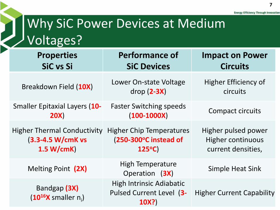
Properties SiC vs Si
Performance of SiC Devices
Impact on Power Circuits
Breakdown Field (10X) Lower On-state Voltage drop (2-3X)
Higher Efficiency of circuits
Smaller Epitaxial Layers (10-20X)
Faster Switching speeds (100-1000X) Compact circuits
Higher Thermal Conductivity (3.3-4.5 W/cmK vs
1.5 W/cmK)
Higher Chip Temperatures (250-300oC instead of
125oC)
Higher pulsed power Higher continuous current densities,
Melting Point (2X) High Temperature Operation (3X) Simple Heat Sink
Bandgap (3X) (1016X smaller ni)
High Intrinsic Adiabatic Pulsed Current Level (3-
10X?) Higher Current Capability
Why SiC Power Devices at Medium Voltages?

8
Ratings of SiC and Si Devices
Maximum Voltage and Current Ratings of UHV SiC Bipolar Devices significantly higher than theoretical capability of Si
Further SiC offers unprecedented margins from failures
15 kV SiC Bipolar
15 kV SiC Bipolar
0 2kV 4kV 6kV 8kV 10kV 40kV 20kV
Si MOSFET/Schottky Diode Si IGBT/ PiN Rectifier
Si GTO Thyristors
Si Thyristor
SiC SuperJT /MOSFET/Schottky
SiC GTO/AST/ PiN Rectifier

9
MOSFET JFET-ON JFET-OFF BJT SJT
Gate Control +20V/0V No Current
+0V/-20V Low Current
+3/0V Current Gain
+3V/0V Current Gain
+3V/0V Current Gain
Current Gain Infinite >1000 ~50 (at rated current)
~30 (at rated current)
>100 (Target at rated current)
Current Rating Very low High Low High High
Fabrication Cost Very High Medium High Low Low
Switching Speed
Medium (Gate Cap) High
Low/Medium (Gate-
Source Cap)
Very low (Minority injection)
High (Low cap, No
Minority)
High Temperature Very Poor Very Good Medium Very Good Very Good
15 kV SiC Switch Comparisons

10
• Low on-resistance of achieved in a 1200 V SJT • High Current gain recorded at Drain Current of 55 A at 25 oC. • Positive temperature co-efficient of on-resistance exhibited,
which is desirable for paralleling multiple devices.
High Current SJTs – output characteristics
4 mm
11
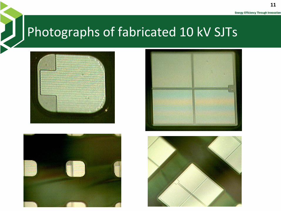
Photographs of fabricated 10 kV SJTs
12
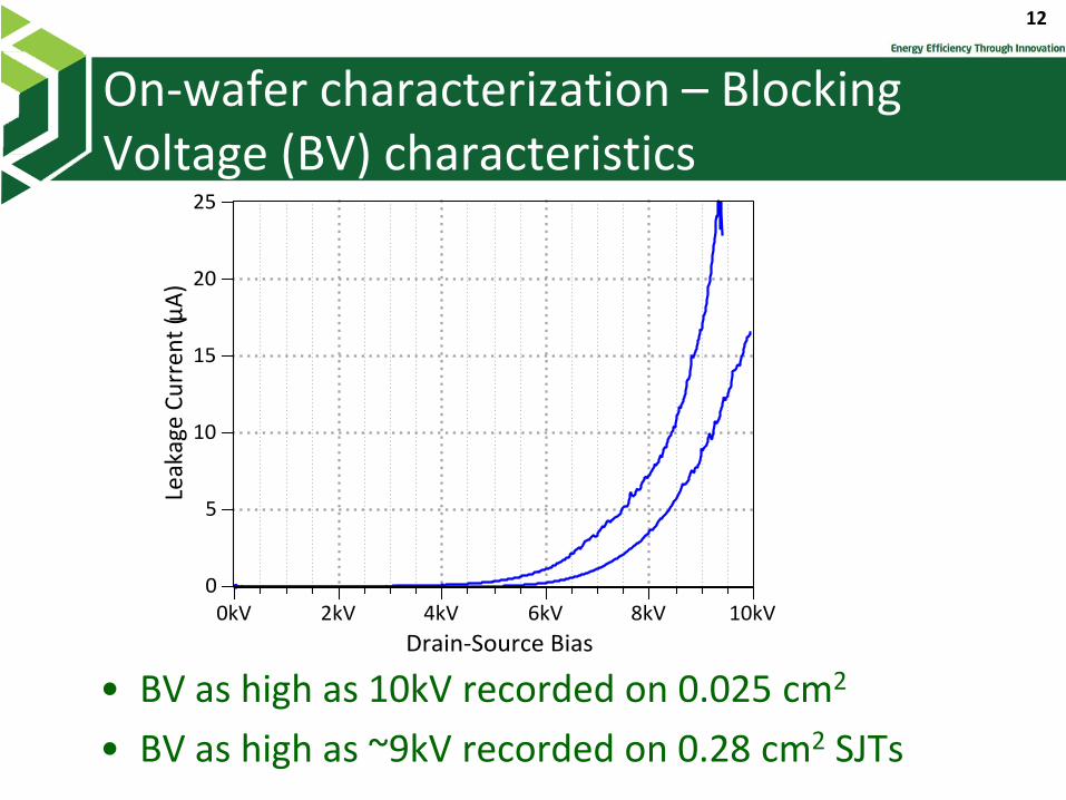
• BV as high as 10kV recorded on 0.025 cm2 • BV as high as ~9kV recorded on 0.28 cm2 SJTs
On-wafer characterization – Blocking Voltage (BV) characteristics

13
• Excellent Gate-Source shorting yield observed for 0.28 cm2 SJTs
Output characteristics of 0.28 cm2 on 10 kV SJTs

14
GeneSiC’s commercial Phase Leg Packaging

15
Module Configuration
Plastic Case (PPS Ryton R-4)
Baseplate
Cathode Power Terminals
(Bottom of Chip)
Gate Terminal
Anode Power Terminal (Top of Chip) Gate Return Terminal
(Anode Potential) SiC Chip on DBC AlN

16
• Current Status Fabrication steps of 1200 V MIDSJT being completed as proof
of concept Design of Silicon Carbide Monolithically integrated
diode/Super Junction Transistor (MIDSJT) being conducted
• Future Efforts in Phase I Characterize devices from present batch and study MIDSJT
concept Complete layout, fabrication and characterization plan for 15
kV/10 A devices
Status and Future Efforts

17
• Principal Investigator: Dr. Siddarth Sundaresan • Program Manager: Dr. Ranbir Singh • Grantee:
GeneSiC Semiconductor Inc. 43670 Trade Center Place Suite 155 Dulles VA 20166 +1 703 996 8200 (ph) [email protected]
Grant Details


