
CLF1G0060-30; CLF1G0060S-30 - Mouser Electronics · CLF1G0060-30 C1 Z5 R1 10 kΩ J1 Z6 Z4 N-F C2...
20
1. Product profile 1.1 General description The CLF1G0060-30 and CLF1G0060S-30 are 30 W general purpose broadband GaN HEMTs usable from DC to 6.0 GHz. [1] Pulsed RF; t p = 100 s; = 10 %. [1] 2-Tone CW; f = 1 MHz. CLF1G0060-30; CLF1G0060S-30 Broadband RF power GaN HEMT Rev. 7 — 5 February 2018 Product data sheet Table 1. CW and pulsed RF application information Typical RF performance at T case = 25 C; I Dq = 70 mA; V DS = 50 V in a class-AB broadband demo board. Test signal f P L G p D (MHz) (W) (dB) (%) 1-Tone CW 500 30 15.6 60.7 1000 30 13.9 50.3 1500 30 13.7 50.8 2000 30 12.6 49 2500 30 14.2 55.6 1-Tone pulsed [1] 500 30 16.6 61 1000 30 15.8 50 1500 30 15.5 52.5 2000 30 14.5 50 2500 30 15.9 59 Table 2. 2-Tone CW application information Typical 2-Tone performance at T case = 25 C; I Dq = 150 mA; V DS = 50 V in a class-AB broadband demo board. Test signal f P L(PEP) IMD3 (MHz) (W) (dBc) 2-Tone CW [1] 500 10 38 1000 10 50 1500 10 45 2000 10 50 2500 10 43
-
Upload
hoangxuyen -
Category
Documents
-
view
220 -
download
0
Transcript of CLF1G0060-30; CLF1G0060S-30 - Mouser Electronics · CLF1G0060-30 C1 Z5 R1 10 kΩ J1 Z6 Z4 N-F C2...

1. Product profile
1.1 General description
The CLF1G0060-30 and CLF1G0060S-30 are 30 W general purpose broadband GaN HEMTs usable from DC to 6.0 GHz.
[1] Pulsed RF; tp = 100 s; = 10 %.
[1] 2-Tone CW; f = 1 MHz.
CLF1G0060-30; CLF1G0060S-30Broadband RF power GaN HEMTRev. 7 — 5 February 2018 Product data sheet
Table 1. CW and pulsed RF application informationTypical RF performance at Tcase = 25 C; IDq = 70 mA; VDS = 50 V in a class-AB broadband demo board.
Test signal f PL Gp D
(MHz) (W) (dB) (%)
1-Tone CW 500 30 15.6 60.7
1000 30 13.9 50.3
1500 30 13.7 50.8
2000 30 12.6 49
2500 30 14.2 55.6
1-Tone pulsed [1] 500 30 16.6 61
1000 30 15.8 50
1500 30 15.5 52.5
2000 30 14.5 50
2500 30 15.9 59
Table 2. 2-Tone CW application informationTypical 2-Tone performance at Tcase = 25 C; IDq = 150 mA; VDS = 50 V in a class-AB broadband demo board.
Test signal f PL(PEP) IMD3
(MHz) (W) (dBc)
2-Tone CW [1] 500 10 38
1000 10 50
1500 10 45
2000 10 50
2500 10 43
CLF1G0060-30_1G0060S-30 All information provided in this document is subject to legal disclaimers. © Ampleon Netherlands B.V. 2018. All rights reserved.
Product data sheet Rev. 7 — 5 February 2018 2 of 19
CLF1G0060-30; CLF1G0060S-30Broadband RF power GaN HEMT
1.2 Features and benefits
Frequency of operation is from DC to 6.0 GHz
30 W general purpose broadband RF Power GaN HEMT
Excellent ruggedness (VSWR = 10 : 1)
High voltage operation (50 V)
Thermally enhanced package
1.3 Applications
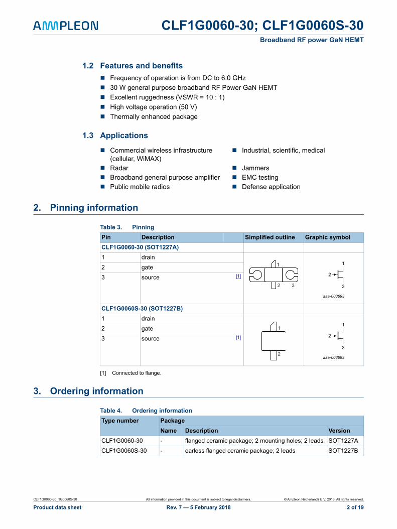
2. Pinning information
[1] Connected to flange.
3. Ordering information
Commercial wireless infrastructure (cellular, WiMAX)
Industrial, scientific, medical
Radar Jammers
Broadband general purpose amplifier EMC testing
Public mobile radios Defense application
Table 3. Pinning
Pin Description Simplified outline Graphic symbol
CLF1G0060-30 (SOT1227A)
1 drain
2 gate
3 source [1]
CLF1G0060S-30 (SOT1227B)
1 drain
2 gate
3 source [1]
1
32
aaa-003693
1
3
2
1
2aaa-003693
1
3
2
Table 4. Ordering information
Type number Package
Name Description Version
CLF1G0060-30 - flanged ceramic package; 2 mounting holes; 2 leads SOT1227A
CLF1G0060S-30 - earless flanged ceramic package; 2 leads SOT1227B

CLF1G0060-30_1G0060S-30 All information provided in this document is subject to legal disclaimers. © Ampleon Netherlands B.V. 2018. All rights reserved.
Product data sheet Rev. 7 — 5 February 2018 3 of 19
CLF1G0060-30; CLF1G0060S-30Broadband RF power GaN HEMT
4. Limiting values
5. Thermal characteristics
[1] Tj is measured via IR scan with case temperature of 85 C and power dissipation of 34 W.
6. Characteristics
Table 5. Limiting valuesIn accordance with the Absolute Maximum Rating System (IEC 60134).
Symbol Parameter Conditions Min Max Unit
VDS drain-source voltage - 150 V
VGS gate-source voltage 8 +3 V
IGF forward gate current external RG = 5 - 11 mA
Tstg storage temperature 65 +150 C
Tj junction temperature measured via IR scan - 250 C
Table 6. Thermal characteristics
Symbol Parameter Conditions Typ Unit
Rth(j-c) thermal resistance from junction to case Tj = 200 C [1] 3.1 K/W
Table 7. DC CharacteristicsTcase = 25 C; unless otherwise specified.
Symbol Parameter Conditions Min Typ Max Unit
V(BR)DSS drain-source breakdown voltage VGS = 7 V; IDS = 7.2 mA
150 - - V
VGS(th) gate-source threshold voltage VDS = 0.1 V; IDS = 7.2 mA
2.4 2 1.6 V
IDSX drain cut-off current VDS = 10 V; VGS = 3 V - 5.1 - A
gfs forward transconductance VDS = 10 V; VGS = 0 V - 1.1 - S
Table 8. RF CharacteristicsTest signal: pulsed RF; f = 3 GHz; tp = 100 s; = 10 %; RF performance at VDS = 50 V; IDq = 70 mA; Tcase = 25 C; unless otherwise specified in a class-AB production circuit.
Symbol Parameter Conditions Min Typ Max Unit
D drain efficiency PL = 30 W 46 54 - %
Gp power gain PL = 30 W 11.8 13.5 - dB
RLin input return loss PL = 30 W - 7 - dB
Pdroop(pulse) pulse droop power PL = 30 W - 0.04 - dB
tr rise time PL = 30 W - 5 - ns
tf fall time PL = 30 W - 5 - ns

CLF1G0060-30_1G0060S-30 All information provided in this document is subject to legal disclaimers. © Ampleon Netherlands B.V. 2018. All rights reserved.
Product data sheet Rev. 7 — 5 February 2018 4 of 19
CLF1G0060-30; CLF1G0060S-30Broadband RF power GaN HEMT
7. Application information
7.1 Demo circuit
Printed-Circuit Board (PCB) material: Taconic RF35, r = 3.5, thickness 30 mils, 1 oz copper on each side.
See Table 9 for list of components.
Fig 1. The broadband amplifier (500 MHz to 2500 MHz) demo circuit outline
Table 9. List of componentsSee Figure 1.
Component Description Value Remarks
A1 GaN bias module v2 - Ampleon
C1, C10 multilayer ceramic chip capacitor 8.2 pF ATC 600F
C2, C7 multilayer ceramic chip capacitor 0.8 pF ATC 600F
C3 electrolytic capacitor 100 nF, 50 V SMD 0805
C4 electrolytic capacitor 10 nF, 50 V SMD 0805
C5 electrolytic capacitor 22 pF, 100 V SMD 0805
C6 electrolytic capacitor 1 nF, 100 V SMD 1206
C8 multilayer ceramic chip capacitor 1.2 pF ATC 600F
C9 multilayer ceramic chip capacitor 0.5 pF ATC 600F
aaa-003736
CLF1G0060-30 500-2500INPUT REV 0 30RF35
CLF1G0060-30 500-2500INPUT REV 0 30RF35
GAN BIASMODULE
Q3
R3
Q2
R2
R1
C16
C15
C11
C17
C8
C1C2
C9
L1
C10C7
C6C3
C4 C5C12
C14 L2
L3

CLF1G0060-30_1G0060S-30 All information provided in this document is subject to legal disclaimers. © Ampleon Netherlands B.V. 2018. All rights reserved.
Product data sheet Rev. 7 — 5 February 2018 5 of 19
CLF1G0060-30; CLF1G0060S-30Broadband RF power GaN HEMT
C11 multilayer ceramic chip capacitor 100 pF ATC 100B
C12 multilayer ceramic chip capacitor 1 nF ATC 700B
C14 electrolytic capacitor 1 F, 100V SMD 1206
C15 electrolytic capacitor 10 F, 100 V SMD 2220
C16 electrolytic capacitor 10 nF, 200 V SMD 1210
C17 electrolytic capacitor 470 F, 63 V PCE3667CT-ND
E1, E2 drain voltage connection -
J1 RF in connector -
J2 RF out connector -
L1 inductor 330 nH 1008CS-331XJB
L2 ferrite bead - 2743019447
L3 inductor - 1 turn, 18 AWG, inner diameter = 4.06 mm
Q1 transistor - CLF1G0060-30
Q2 transistor - NXP BC857B
Q3 transistor - NXP PSMN8R2-80YS
R1 resistor 10 k Vishay Dale
R2 resistor 10 Vishay Dale
R3 resistor 0.005 RL7520WT-R005-F
Z1, Z2, Z3, Z4, Z5, Z6, Z7, Z8, Z9, Z10, Z11, Z12, Z13
microstrip lines -
Table 9. List of components …continuedSee Figure 1.
Component Description Value Remarks

xxxxxxxxxxxxxxxxxxxxx xxxxxxxxxxxxxxxxxxxxxxxxxx xxxxxxx x x x xxxxxxxxxxxxxxxxxxxxxxxxxxxxxx xxxxxxxxxxxxxxxxxxx xx xx xxxxx xxxxxxxxxxxxxxxxxxxxxxxxxxx xxxxxxxxxxxxxxxxxxx xxxxxx xxxxxxxxxxxxxxxxxxxxxxxxxxxxxxxxxxx xxxxxxxxxxxx x x xxxxxxxxxxxxxxxxxxxxx xxxxxxxxxxxxxxxxxxxxxxxxxxxxxx xxxxx xxxxxxxxxxxxxxxxxxxxxxxxxxxxxxxxxxxxxxxxxxxxxxxxxx xxxxxxxx xxxxxxxxxxxxxxxxxxxxxxxxx xxxxxxxxxxxxxxxxxxxx xxx
CL
F1
G0
060-30_1G
0060S
-30A
ll information provid
ed in this documen
t is subject to legal disclaimers.
© A
mpleon N
etherla
nds B.V
. 2018. A
ll rights reserved.
Pro
du
ct data sh
eet
Rev. 7 —
5 Feb
rua
ry 2018
6 o
f 19
CL
F1G
0060-30; CL
F1G
0060S-30
Bro
ad
ba
nd
RF
po
we
r GaN
HE
MT
See Table 9 for a list of components.
Fig 2. The broadband amplifier (500 MHz to 2500 MHz) demo circuit schematic
GND
IN2
DA1
Q2BC857B
Q1CLF1G0060-30
C1 Z5
R110 kΩ
Z4Z6J1
N-F
C20.3 pF
5.6 pF 376 x 67.5 mil605 x 67.5 mil 210 x 67.5 mil
GAN BIAS MODULE
GS
VGFBC
BE
34
575
101112
1
6
9
GND
GND
C70.8 pF
C81.2 pF
Z7
60 x 201 mil
Z8
59 x 201 milZ2 Z1
R2
10 Ω
R4
200 Ω
40 x 562 mil
Z3
136 x 67.5 mil 168 x 562 mil
L35 nH
L1330 nH
C15470 μF
E1 E2+50 V GND
Q3PSMN8R2-80YS
32 14
5
Z11
572 x 138 mil
Z12 C10
5.6 pF
C14
10 F
C13
10 nF
C12
1 nF
C11
100 pF
C6
1 nF
C5
22 pF
C4
10 nF
C3
100 nF
400 x 98 mil
Z13
118 x 67.5 mil
Z9
273 x 201 mil
Z10
58 x 138 mil
J2
N-F
aaa-003790
C90.5 pF

CLF1G0060-30_1G0060S-30 All information provided in this document is subject to legal disclaimers. © Ampleon Netherlands B.V. 2018. All rights reserved.
Product data sheet Rev. 7 — 5 February 2018 7 of 19
CLF1G0060-30; CLF1G0060S-30Broadband RF power GaN HEMT
7.2 Application test results
[1] Pulsed RF; tp = 100 s; = 10 %.
[1] 2-Tone CW; f = 1 MHz.
Table 10. CW and pulsed RF application informationTypical RF performance at Tcase = 25 C; IDq = 70 mA; VDS = 50 V in a class-AB broadband demo board.
Test signal f PL Gp D
(MHz) (W) (dB) (%)
1-Tone CW 500 30 15.6 60.7
1000 30 13.9 50.3
1500 30 13.7 50.8
2000 30 12.6 49
2500 30 14.2 55.6
1-Tone pulsed [1] 500 30 16.6 61
1000 30 15.8 50
1500 30 15.5 52.5
2000 30 14.5 50
2500 30 15.9 59
Table 11. 2-Tone CW application informationTypical 2-Tone performance at Tcase = 25 C; IDq = 150 mA; VDS = 50 V in a class-AB broadband demo board.
Test signal f PL(PEP) IMD3
(MHz) (W) (dBc)
2-Tone CW [1] 500 10 38
1000 10 50
1500 10 45
2000 10 50
2500 10 43

CLF1G0060-30_1G0060S-30 All information provided in this document is subject to legal disclaimers. © Ampleon Netherlands B.V. 2018. All rights reserved.
Product data sheet Rev. 7 — 5 February 2018 8 of 19
CLF1G0060-30; CLF1G0060S-30Broadband RF power GaN HEMT
7.3 Graphical data
The following figures are measured in a broadband amplifier demo board from 500 MHz to 2500 MHz.
7.3.1 1-Tone CW RF performance
VDS = 50 V; IDq = 70 mA; PL = 30 W. VDS = 50 V; IDq = 70 mA.
(1) Gp at f = 500 MHz
(2) Gp at f = 1500 MHz
(3) Gp at f = 2500 MHz
(4) D at f = 500 MHz
(5) D at f = 1500 MHz
(6) D at f = 2500 MHz
Fig 3. Power gain and drain efficiency as function of frequency; typical values
Fig 4. Power gain and drain efficiency as function of output power; typical values
aaa-003960
0 500 1000 1500 2000 2500 30000 10
4 25
8 40
12 55
16 70
f (MHz)
Gppp(dB)
ηD(%)
Gp
ηD
aaa-003961
34 36 38 40 42 44 46 480 0
6 20
12 40
18 60
24 80
PL (dBm)
Gppp(dB)
ηD(%)
(1)
(2)(3)
(4)
(5)(6)

CLF1G0060-30_1G0060S-30 All information provided in this document is subject to legal disclaimers. © Ampleon Netherlands B.V. 2018. All rights reserved.
Product data sheet Rev. 7 — 5 February 2018 9 of 19
CLF1G0060-30; CLF1G0060S-30Broadband RF power GaN HEMT
7.3.2 1-Tone pulsed RF performance
VDS = 50 V; IDq = 70 mA; PL = 30 W; tp = 100 s; = 10 %.
VDS = 50 V; IDq = 70 mA; tp = 100 s; = 10 %.
(1) Gp at f = 500 MHz
(2) Gp at f = 1500 MHz
(3) Gp at f = 2500 MHz
(4) D at f = 500 MHz
(5) D at f = 1500 MHz
(6) D at f = 2500 MHz
Fig 5. Power gain and drain efficiency as function of frequency; typical values
Fig 6. Power gain and drain efficiency gain as function of output power; typical values
aaa-003962
0 500 1000 1500 2000 2500 30000 10
3 20
6 30
9 40
12 50
15 60
18 70
f (MHz)
Gppp(dB)
ηD(%)Gp
ηD
aaa-003963
34 36 38 40 42 44 46 480 0
6 20
12 40
18 60
24 80
PL (dBm)
Gppp(dB)
ηD(%)
(1)
(2)(3)
(4)
(5)
(6)

CLF1G0060-30_1G0060S-30 All information provided in this document is subject to legal disclaimers. © Ampleon Netherlands B.V. 2018. All rights reserved.
Product data sheet Rev. 7 — 5 February 2018 10 of 19
CLF1G0060-30; CLF1G0060S-30Broadband RF power GaN HEMT
7.3.3 2-Tone CW performance
7.4 Bias module
The bias module information for the GaN HEMT amplifier is described in application note AN11130.
8. Test information
8.1 Ruggedness in class-AB operation
The CLF1G0060-30 and CLF1G0060S-30 are capable of withstanding a load mismatch corresponding to VSWR = 10 : 1 through all phases under the following conditions: VDS = 50 V; PL = 30 W (pulsed RF), f = 3000 MHz.
8.2 Load pull impedance information
The measured load pull impedances are shown below. Impedance reference plane defined at device leads. Measurements performed with Ampleon test fixtures. Test temperature set at 25 C with a pulsed CW signal; tp = 100 s; = 10 %; RF performance at VDS = 50 V; IDq = 50 mA.
VDS = 50 V; IDq = 150 mA; f = 1 MHz.
(1) f = 500 MHz
(2) f = 1500 MHz
(3) f = 2500 MHz
VDS = 50 V; IDq = 150 mA; PL(PEP) =10 W.
(1) f = 10 kHz
(2) f = 30 kHz
(3) f = 100 kHz
(4) f = 300 kHz
(5) f = 1 MHz
(6) f = 3 MHz
Fig 7. Third order intermodulation distortion as a function of peak envelope power; typical values
Fig 8. Third-order intermodulation distortion as function of frequency and tone spacing; typical values
aaa-003964
1 10 102-60
-50
-40
-30
-20
-10
0
PL(PEP) (W)
IMD3(dBc)
(1)
(2)
(3)
aaa-004003
500 900 1300 1700 2100 2500-60
-50
-40
-30
-20
f (MHz)
IMD3(dBc)
(1)(3)(2)(4)(5)(6)

CLF1G0060-30_1G0060S-30 All information provided in this document is subject to legal disclaimers. © Ampleon Netherlands B.V. 2018. All rights reserved.
Product data sheet Rev. 7 — 5 February 2018 11 of 19
CLF1G0060-30; CLF1G0060S-30Broadband RF power GaN HEMT
ZS is the measured source pull impedance presented to the device. ZL is the measured load pull impedance presented to the device.
Table 12. Typical impedanceTypical values unless otherwise specified.
f ZS ZL (maximum PL(M)) ZL (maximum D)
(MHz) () () ()
2140 1.4 4j 14 + 5.4j 12.5 + 9.7j
2500 2.8 6j 10.5 + 2.5j 7.6 + 5.6j
2700 2.8 7.5j 10.7 + 1.3j 7.6 + 4.3j
3000 3.0 10j 9.1 + 3.5j 7.7 + 4.2j
3300 3.0 11.5j 9.4 + 1.2j 7.6 + 2.5j
3500 3.0 13j 9.5 7.2 + 1.35j
3700 3.5 14.4j 9.4 1.1j 7.3 0.05j
4000 3.7 20.3j 9.3 2.4j 7.7 1.2j
Fig 9. Definition of transistor impedance
aaa-003694
drain
source
ZS ZL
gate

CLF1G0060-30_1G0060S-30 All information provided in this document is subject to legal disclaimers. © Ampleon Netherlands B.V. 2018. All rights reserved.
Product data sheet Rev. 7 — 5 February 2018 12 of 19
CLF1G0060-30; CLF1G0060S-30Broadband RF power GaN HEMT
8.3 Packaged S-parameter data
Table 13. S-parameterSmall signal; VDS = 50 V; IDq = 50 mA; ZS = ZL = 50 .
f(MHz)
S11 S21 S12 S22
Magnitude(ratio)
Angle(degree)
Magnitude(ratio)
Angle(degree)
Magnitude(ratio)
Angle(degree)
Magnitude(ratio)
Angle(degree)
100 0.9302 76.396 44.515 135.22 0.016195 46.871 0.7376 43.407
200 0.87436 115.47 29.415 111.96 0.021253 25.279 0.55438 65.523
300 0.8537 134.97 21.02 98.876 0.022516 13.903 0.47582 77.762
400 0.8464 146.22 16.096 89.855 0.02261 6.6529 0.44954 86.181
500 0.8446 153.57 12.919 82.761 0.022198 1.4192 0.44849 92.826
600 0.84548 158.81 10.71 76.739 0.021498 2.6237 0.46041 98.482
700 0.84785 162.82 9.0883 71.392 0.020604 5.8352 0.47921 103.5
800 0.85112 166.05 7.8465 66.516 0.019567 8.375 0.50159 108.06
900 0.85494 168.77 6.8655 61.995 0.018424 10.302 0.5256 112.27
1000 0.85908 171.15 6.0713 57.758 0.017205 11.612 0.5501 116.19
1100 0.86338 173.27 5.4157 53.759 0.015936 12.256 0.57433 119.86
1200 0.86774 175.22 4.866 49.966 0.014644 12.138 0.59785 123.33
1300 0.87206 177.04 4.3993 46.356 0.01336 11.113 0.62038 126.6
1400 0.8763 178.75 3.9988 42.911 0.012117 8.9845 0.64176 129.7
1500 0.88039 179.61 3.6521 39.616 0.010958 5.505 0.66191 132.65
1600 0.88432 178.03 3.3496 36.459 0.0099386 0.40868 0.68081 135.46
1700 0.88806 176.49 3.0841 33.428 0.0091267 6.4893 0.69846 138.14
1800 0.8916 175 2.8497 30.514 0.0085991 15.099 0.7149 140.7
1900 0.89493 173.53 2.6416 27.709 0.008424 24.853 0.73019 143.15
2000 0.89806 172.09 2.4562 25.005 0.0086339 34.74 0.74438 145.5
2100 0.90098 170.67 2.2902 22.395 0.0092114 43.73 0.75755 147.76
2200 0.9037 169.26 2.1411 19.872 0.0101 51.208 0.76975 149.93
2300 0.90622 167.87 2.0067 17.429 0.011233 57.053 0.78106 152.02
2400 0.90856 166.48 1.8852 15.062 0.012549 61.439 0.79154 154.04
2500 0.91072 165.11 1.775 12.766 0.014001 64.635 0.80125 155.99
2600 0.91272 163.74 1.6748 10.534 0.015556 66.902 0.81025 157.88
2700 0.91455 162.37 1.5835 8.3639 0.017191 68.455 0.8186 159.71
2800 0.91623 161 1.5001 6.2502 0.01889 69.459 0.82634 161.49
2900 0.91777 159.63 1.4237 4.1894 0.020642 70.039 0.83353 163.22
3000 0.91917 158.27 1.3535 2.1779 0.022441 70.288 0.8402 164.91
3100 0.92044 156.89 1.289 0.21252 0.024281 70.278 0.84641 166.55
3200 0.9216 155.52 1.2296 1.71 0.02616 70.06 0.85218 168.16
3300 0.92264 154.14 1.1748 3.5925 0.028076 69.675 0.85755 169.73
3400 0.92357 152.75 1.1241 5.4376 0.030027 69.154 0.86255 171.27
3500 0.92441 151.35 1.0771 7.2479 0.032015 68.521 0.8672 172.78
3600 0.92515 149.94 1.0336 9.0257 0.034039 67.795 0.87155 174.26
3700 0.92579 148.53 0.99314 10.773 0.036099 66.989 0.87559 175.72

CLF1G0060-30_1G0060S-30 All information provided in this document is subject to legal disclaimers. © Ampleon Netherlands B.V. 2018. All rights reserved.
Product data sheet Rev. 7 — 5 February 2018 13 of 19
CLF1G0060-30; CLF1G0060S-30Broadband RF power GaN HEMT
3800 0.92635 147.1 0.95551 12.493 0.038198 66.115 0.87937 177.15
3900 0.92683 145.65 0.92046 14.186 0.040336 65.183 0.8829 178.57
4000 0.92723 144.2 0.88777 15.855 0.042516 64.2 0.88619 179.97
4100 0.92756 142.73 0.85724 17.501 0.044737 63.171 0.88927 178.65
4200 0.92781 141.24 0.82871 19.126 0.047003 62.101 0.89215 177.28
4300 0.928 139.73 0.802 20.732 0.049315 60.994 0.89484 175.93
4400 0.92812 138.2 0.77698 22.32 0.051676 59.853 0.89735 174.58
4500 0.92818 136.66 0.75351 23.891 0.054087 58.68 0.8997 173.25
4600 0.92818 135.09 0.73149 25.447 0.05655 57.477 0.9019 171.92
4700 0.92812 133.5 0.71079 26.99 0.059068 56.245 0.90396 170.6
4800 0.928 131.89 0.69133 28.519 0.061644 54.986 0.90588 169.28
4900 0.92783 130.25 0.67301 30.038 0.064279 53.699 0.90767 167.97
5000 0.92761 128.59 0.65576 31.546 0.066975 52.387 0.90935 166.66
5100 0.92734 126.9 0.63949 33.046 0.069736 51.047 0.91092 165.35
5200 0.92701 125.17 0.62415 34.537 0.072563 49.682 0.91238 164.04
5300 0.92664 123.42 0.60968 36.022 0.075459 48.291 0.91375 162.73
5400 0.92622 121.64 0.596 37.501 0.078426 46.874 0.91502 161.42
5500 0.92576 119.83 0.58307 38.975 0.081467 45.43 0.9162 160.1
5600 0.92525 117.98 0.57085 40.446 0.084583 43.959 0.9173 158.78
5700 0.9247 116.1 0.55929 41.914 0.087778 42.461 0.91832 157.45
5800 0.92411 114.18 0.54834 43.38 0.091053 40.935 0.91927 156.12
5900 0.92348 112.22 0.53797 44.846 0.094411 39.381 0.92014 154.77
6000 0.92282 110.23 0.52814 46.311 0.097853 37.797 0.92095 153.42
Table 13. S-parameter …continuedSmall signal; VDS = 50 V; IDq = 50 mA; ZS = ZL = 50 .
f(MHz)
S11 S21 S12 S22
Magnitude(ratio)
Angle(degree)
Magnitude(ratio)
Angle(degree)
Magnitude(ratio)
Angle(degree)
Magnitude(ratio)
Angle(degree)

CLF1G0060-30_1G0060S-30 All information provided in this document is subject to legal disclaimers. © Ampleon Netherlands B.V. 2018. All rights reserved.
Product data sheet Rev. 7 — 5 February 2018 14 of 19
CLF1G0060-30; CLF1G0060S-30Broadband RF power GaN HEMT
9. Package outline
Fig 10. Package outline SOT1227A
ReferencesOutlineversion
Europeanprojection Issue date
IEC JEDEC JEITA
SOT1227A 12-06-0813-10-14
Flanged ceramic package; 2 mounting holes; 2 leads SOT1227A
sot1227a_po
Unit(1)
mmmaxnommin
3.68
2.84
1.40
1.14
5.21
4.95
4.17
3.96
8.64
7.62
1.70
1.45
A
Dimensions
b D1 E E1 H p
2.67
2.41
Q U1
14.10
13.84
4.19
3.94
U2
inchesmaxnommin
0.145
0.112
0.055
0.045
0.15
0.08
c
0.006
0.003
5.18
4.98
D
0.204
0.196
0.205
0.195
1.14
0.89
4.19
3.94
F
0.045
0.035
0.165
0.155
0.164
0.156
0.340
0.300
0.067
0.057
w1
0.259.53 0.380
0.01 0.0150.105
0.095
q
0.165
0.155
0.555
0.5450.375
Note1. Millimeter dimensions are derived from the original inch dimensions.
w2
scale
5 mm0
b
D
A
F
D1
q
U1
C
B
U2
A
H p
w1 A B
w2 A B
w1 A B
w1 A B
EE1
c
Qw1 C
1
3
2

CLF1G0060-30_1G0060S-30 All information provided in this document is subject to legal disclaimers. © Ampleon Netherlands B.V. 2018. All rights reserved.
Product data sheet Rev. 7 — 5 February 2018 15 of 19
CLF1G0060-30; CLF1G0060S-30Broadband RF power GaN HEMT
Fig 11. Package outline SOT1227B
ReferencesOutlineversion
Europeanprojection Issue date
IEC JEDEC JEITA
SOT1227B 12-06-0813-10-15
Earless Flanged ceramic package; 2 leads SOT1227B
sot1227b_po
Unit(1)
mmmaxnommin
3.68
2.84
1.40
1.14
5.21
4.95
4.17
3.96
8.64
7.62
5.21
4.95
4.19
3.94
A
Dimensions
b D1 E E1 H Q
1.70
1.45
U1 w1
inchesmaxnommin
0.145
0.112
0.055
0.045
0.15
0.08
c
0.006
0.003
5.18
4.98
D
0.204
0.196
0.205
0.195
1.07
0.97
4.19
3.94
F
0.042
0.038
0.165
0.155
0.164
0.156
0.340
0.300
0.205
0.195
0.165
0.155
0.25
0.010.067
0.057
U2
Note1. Millimeter dimensions are derived from the original inch dimensions.
scale
5 mm0
b
D
F
3
1
2
U1
D1
H EE1
c
Qw2 B
w1 A B
A
U2
w2
0.380
0.015
A
w1 A D
w2 A B
B

CLF1G0060-30_1G0060S-30 All information provided in this document is subject to legal disclaimers. © Ampleon Netherlands B.V. 2018. All rights reserved.
Product data sheet Rev. 7 — 5 February 2018 16 of 19
CLF1G0060-30; CLF1G0060S-30Broadband RF power GaN HEMT
10. Handling information
10.1 ESD Sensitivity
[1] Classification 1B is granted to any part that passes after exposure to an ESD pulse of 500 V, but fails after exposure to an ESD pulse of 1000 V.
11. Abbreviations
12. Revision history
Table 14. ESD sensitivity
ESD model Class
Human Body Model (HBM); According JEDEC standard JESD22-A114F 1B [1]
Table 15. Abbreviations
Acronym Description
AWG American Wire Gauge
CW Continuous Wave
EMC ElectroMagnetic Compatibility
ESD ElectroStatic Discharge
GaN Gallium Nitride
HEMT High Electron Mobility Transistor
SMD Surface Mounted Device
VSWR Voltage Standing-Wave Ratio
WiMAX Worldwide Interoperability for Microwave Access
Table 16. Revision history
Document ID Release date Data sheet status Change notice Supersedes
CLF1G0060-30_1G0060S-30 v.7 20180205 Product data sheet - CLF1G0060-30_1G0060S-30 v.6
Modifications: • Table 9 on page 4: L1 remark updated
• Figure 2 on page 6: L1 value updated
CLF1G0060-30_1G0060S-30 v.6 20160218 Product data sheet - CLF1G0060-30_1G0060S-30#5
CLF1G0060-30_1G0060S-30#5 20150901 Objective data sheet - CLF1G0060-30_1G0060S-30 v.4
CLF1G0060-30_1G0060S-30 v.4 20130620 Objective data sheet - CLF1G0060-30_1G0060S-30 v.3
CLF1G0060-30_1G0060S-30 v.3 20130327 Objective data sheet - CLF1G0060-30_1G0060S-30 v.2
CLF1G0060-30_1G0060S-30 v.2 20130129 Objective data sheet - CLF1G0060-30_1G0060S-30 v.1
CLF1G0060-30_1G0060S-30 v.1 20121008 Objective data sheet - -

CLF1G0060-30_1G0060S-30 All information provided in this document is subject to legal disclaimers. © Ampleon Netherlands B.V. 2018. All rights reserved.
Product data sheet Rev. 7 — 5 February 2018 17 of 19
CLF1G0060-30; CLF1G0060S-30Broadband RF power GaN HEMT
13. Legal information
13.1 Data sheet status
[1] Please consult the most recently issued document before initiating or completing a design.
[2] The term ‘short data sheet’ is explained in section “Definitions”.
[3] The product status of device(s) described in this document may have changed since this document was published and may differ in case of multiple devices. The latest product status information is available on the Internet at URL http://www.ampleon.com.
13.2 Definitions
Draft — The document is a draft version only. The content is still under internal review and subject to formal approval, which may result in modifications or additions. Ampleon does not give any representations or warranties as to the accuracy or completeness of information included herein and shall have no liability for the consequences of use of such information.
Short data sheet — A short data sheet is an extract from a full data sheet with the same product type number(s) and title. A short data sheet is intended for quick reference only and should not be relied upon to contain detailed and full information. For detailed and full information see the relevant full data sheet, which is available on request via the local Ampleon sales office. In case of any inconsistency or conflict with the short data sheet, the full data sheet shall prevail.
Product specification — The information and data provided in a Product data sheet shall define the specification of the product as agreed between Ampleon and its customer, unless Ampleon and customer have explicitly agreed otherwise in writing. In no event however, shall an agreement be valid in which the Ampleon product is deemed to offer functions and qualities beyond those described in the Product data sheet.
13.3 Disclaimers
Limited warranty and liability — Information in this document is believed to be accurate and reliable. However, Ampleon does not give any representations or warranties, expressed or implied, as to the accuracy or completeness of such information and shall have no liability for the consequences of use of such information. Ampleon takes no responsibility for the content in this document if provided by an information source outside of Ampleon.
In no event shall Ampleon be liable for any indirect, incidental, punitive, special or consequential damages (including - without limitation - lost profits, lost savings, business interruption, costs related to the removal or replacement of any products or rework charges) whether or not such damages are based on tort (including negligence), warranty, breach of contract or any other legal theory.
Notwithstanding any damages that customer might incur for any reason whatsoever, Ampleon’s aggregate and cumulative liability towards customer for the products described herein shall be limited in accordance with the Terms and conditions of commercial sale of Ampleon.
Right to make changes — Ampleon reserves the right to make changes to information published in this document, including without limitation specifications and product descriptions, at any time and without notice. This document supersedes and replaces all information supplied prior to the publication hereof.
Suitability for use — Ampleon products are not designed, authorized or warranted to be suitable for use in life support, life-critical or safety-critical systems or equipment, nor in applications where failure or malfunction of an
Ampleon product can reasonably be expected to result in personal injury, death or severe property or environmental damage. Ampleon and its suppliers accept no liability for inclusion and/or use of Ampleon products in such equipment or applications and therefore such inclusion and/or use is at the customer’s own risk.
Applications — Applications that are described herein for any of these products are for illustrative purposes only. Ampleon makes no representation or warranty that such applications will be suitable for the specified use without further testing or modification.
Customers are responsible for the design and operation of their applications and products using Ampleon products, and Ampleon accepts no liability for any assistance with applications or customer product design. It is customer’s sole responsibility to determine whether the Ampleon product is suitable and fit for the customer’s applications and products planned, as well as for the planned application and use of customer’s third party customer(s). Customers should provide appropriate design and operating safeguards to minimize the risks associated with their applications and products.
Ampleon does not accept any liability related to any default, damage, costs or problem which is based on any weakness or default in the customer’s applications or products, or the application or use by customer’s third party customer(s). Customer is responsible for doing all necessary testing for the customer’s applications and products using Ampleon products in order to avoid a default of the applications and the products or of the application or use by customer’s third party customer(s). Ampleon does not accept any liability in this respect.
Limiting values — Stress above one or more limiting values (as defined in the Absolute Maximum Ratings System of IEC 60134) will cause permanent damage to the device. Limiting values are stress ratings only and (proper) operation of the device at these or any other conditions above those given in the Recommended operating conditions section (if present) or the Characteristics sections of this document is not warranted. Constant or repeated exposure to limiting values will permanently and irreversibly affect the quality and reliability of the device.
Terms and conditions of commercial sale — Ampleon products are sold subject to the general terms and conditions of commercial sale, as published at http://www.ampleon.com/terms, unless otherwise agreed in a valid written individual agreement. In case an individual agreement is concluded only the terms and conditions of the respective agreement shall apply. Ampleon hereby expressly objects to applying the customer’s general terms and conditions with regard to the purchase of Ampleon products by customer.
No offer to sell or license — Nothing in this document may be interpreted or construed as an offer to sell products that is open for acceptance or the grant, conveyance or implication of any license under any copyrights, patents or other industrial or intellectual property rights.
Export control — This document as well as the item(s) described herein may be subject to export control regulations. Export might require a prior authorization from competent authorities.
Document status[1][2] Product status[3] Definition
Objective [short] data sheet Development This document contains data from the objective specification for product development.
Preliminary [short] data sheet Qualification This document contains data from the preliminary specification.
Product [short] data sheet Production This document contains the product specification.
CLF1G0060-30_1G0060S-30 All information provided in this document is subject to legal disclaimers. © Ampleon Netherlands B.V. 2018. All rights reserved.
Product data sheet Rev. 7 — 5 February 2018 18 of 19
CLF1G0060-30; CLF1G0060S-30Broadband RF power GaN HEMT
Non-automotive qualified products — Unless this data sheet expressly states that this specific Ampleon product is automotive qualified, the product is not suitable for automotive use. It is neither qualified nor tested in accordance with automotive testing or application requirements. Ampleon accepts no liability for inclusion and/or use of non-automotive qualified products in automotive equipment or applications.
In the event that customer uses the product for design-in and use in automotive applications to automotive specifications and standards, customer (a) shall use the product without Ampleon’s warranty of the product for such automotive applications, use and specifications, and (b) whenever customer uses the product for automotive applications beyond Ampleon’s specifications such use shall be solely at customer’s own risk, and (c) customer fully indemnifies Ampleon for any liability, damages or failed product claims resulting from customer design and use of the product for automotive applications beyond Ampleon’s standard warranty and Ampleon’s product specifications.
Translations — A non-English (translated) version of a document is for reference only. The English version shall prevail in case of any discrepancy between the translated and English versions.
13.4 TrademarksNotice: All referenced brands, product names, service names and trademarks are the property of their respective owners.
Any reference or use of any ‘NXP’ trademark in this document or in or on the surface of Ampleon products does not result in any claim, liability or entitlement vis-à-vis the owner of this trademark. Ampleon is no longer part of the NXP group of companies and any reference to or use of the ‘NXP’ trademarks will be replaced by reference to or use of Ampleon’s own trademarks.
14. Contact information
For more information, please visit: http://www.ampleon.com
For sales office addresses, please visit: http://www.ampleon.com/sales

CLF1G0060-30; CLF1G0060S-30Broadband RF power GaN HEMT
© Ampleon Netherlands B.V. 2018. All rights reserved.
For more information, please visit: http://www.ampleon.comFor sales office addresses, please visit: http://www.ampleon.com/sales
Date of release: 5 February 2018
Document identifier: CLF1G0060-30_1G0060S-30
Please be aware that important notices concerning this document and the product(s)described herein, have been included in section ‘Legal information’.
15. Contents
1 Product profile . . . . . . . . . . . . . . . . . . . . . . . . . . 11.1 General description . . . . . . . . . . . . . . . . . . . . . 11.2 Features and benefits . . . . . . . . . . . . . . . . . . . . 21.3 Applications . . . . . . . . . . . . . . . . . . . . . . . . . . . 2
2 Pinning information. . . . . . . . . . . . . . . . . . . . . . 2
3 Ordering information. . . . . . . . . . . . . . . . . . . . . 2
4 Limiting values. . . . . . . . . . . . . . . . . . . . . . . . . . 3
5 Thermal characteristics . . . . . . . . . . . . . . . . . . 3
6 Characteristics. . . . . . . . . . . . . . . . . . . . . . . . . . 3
7 Application information. . . . . . . . . . . . . . . . . . . 47.1 Demo circuit . . . . . . . . . . . . . . . . . . . . . . . . . . . 47.2 Application test results . . . . . . . . . . . . . . . . . . . 77.3 Graphical data . . . . . . . . . . . . . . . . . . . . . . . . . 87.3.1 1-Tone CW RF performance. . . . . . . . . . . . . . . 87.3.2 1-Tone pulsed RF performance . . . . . . . . . . . . 97.3.3 2-Tone CW performance . . . . . . . . . . . . . . . . 107.4 Bias module . . . . . . . . . . . . . . . . . . . . . . . . . . 10
8 Test information . . . . . . . . . . . . . . . . . . . . . . . . 108.1 Ruggedness in class-AB operation . . . . . . . . 108.2 Load pull impedance information . . . . . . . . . . 108.3 Packaged S-parameter data. . . . . . . . . . . . . . 12
9 Package outline . . . . . . . . . . . . . . . . . . . . . . . . 14
10 Handling information. . . . . . . . . . . . . . . . . . . . 1610.1 ESD Sensitivity . . . . . . . . . . . . . . . . . . . . . . . . 16
11 Abbreviations. . . . . . . . . . . . . . . . . . . . . . . . . . 16
12 Revision history. . . . . . . . . . . . . . . . . . . . . . . . 16
13 Legal information. . . . . . . . . . . . . . . . . . . . . . . 1713.1 Data sheet status . . . . . . . . . . . . . . . . . . . . . . 1713.2 Definitions. . . . . . . . . . . . . . . . . . . . . . . . . . . . 1713.3 Disclaimers . . . . . . . . . . . . . . . . . . . . . . . . . . . 1713.4 Trademarks. . . . . . . . . . . . . . . . . . . . . . . . . . . 18
14 Contact information. . . . . . . . . . . . . . . . . . . . . 18
15 Contents . . . . . . . . . . . . . . . . . . . . . . . . . . . . . . 19

Mouser Electronics
Authorized Distributor
Click to View Pricing, Inventory, Delivery & Lifecycle Information: Ampleon:
CLF1G0060-30U
NXP:
CLF1G0060S-30U


![CLF1G0060-30; CLF1G0060S-30 - · PDF fileThe CLF1G0060-30 and CLF1G0060S-30 are 30W general purpose broadband GaN HEMTs usable from DCto6.0GHz. Table 1. CW and pulsed RF [1] Pulsed](https://static.fdocuments.net/doc/165x107/5abd73e87f8b9aa15e8b972d/clf1g0060-30-clf1g0060s-30-the-clf1g0060-30-and-clf1g0060s-30-are-30w-general.jpg)
